SAGEMCOM BROANDS HILONCV2 GPRS module User Manual
SAGEMCOM SAS GPRS module
UserManual.wiki
>
SAGEMCOM BROANDS
>
HILONCV2 User Manual
User manual
Navigation menu
Upload a User Manual
Namespaces
Wiki Guide
HTML
PDF
Info
Views
User Manual
Discussion / Help
Navigation
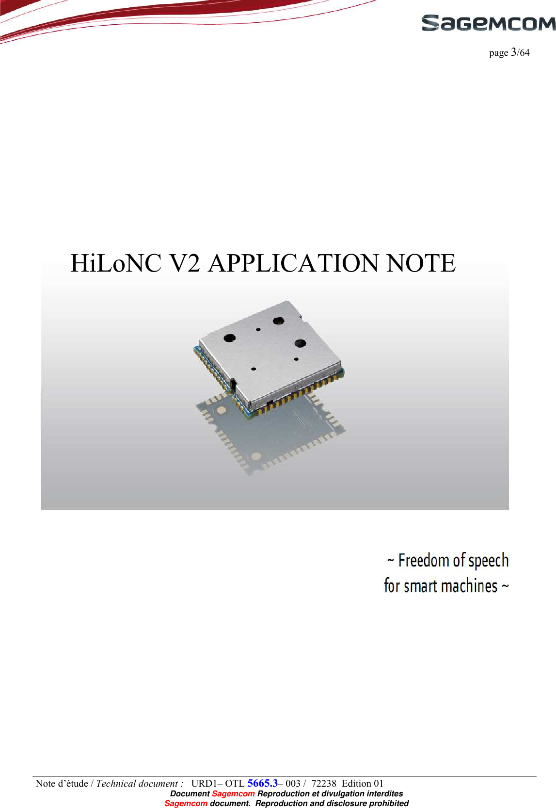
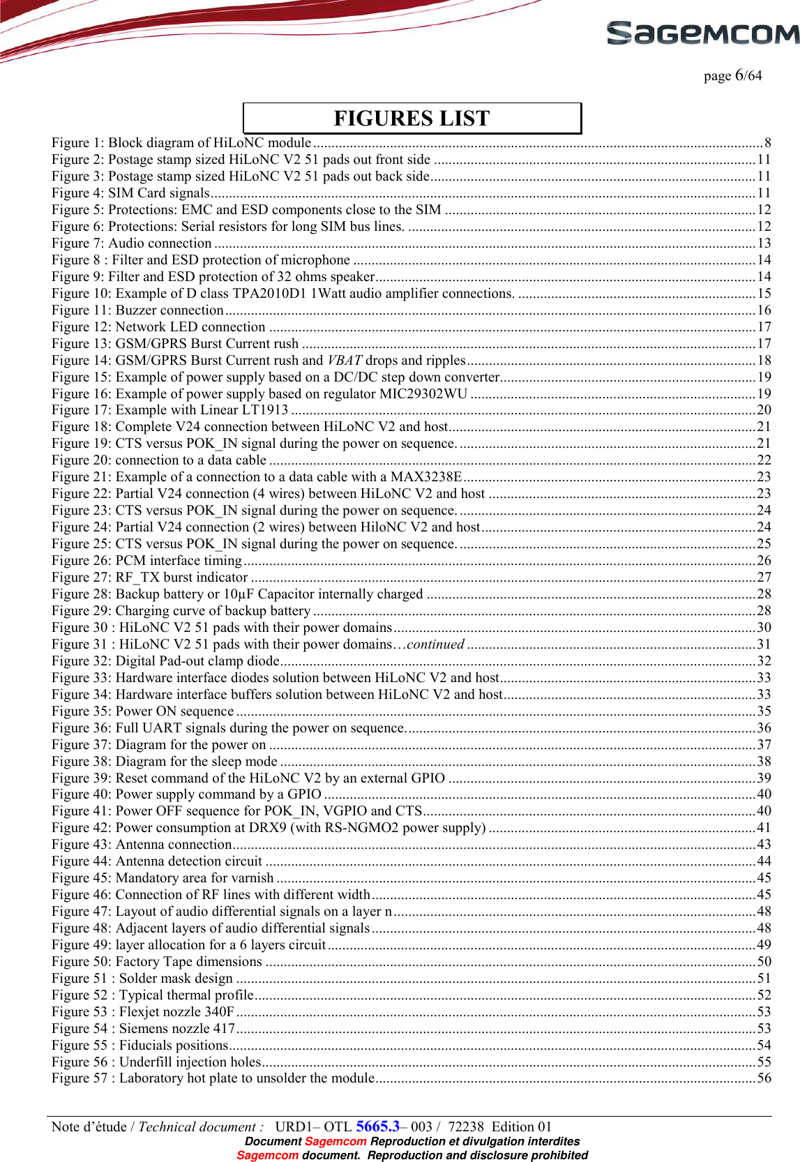
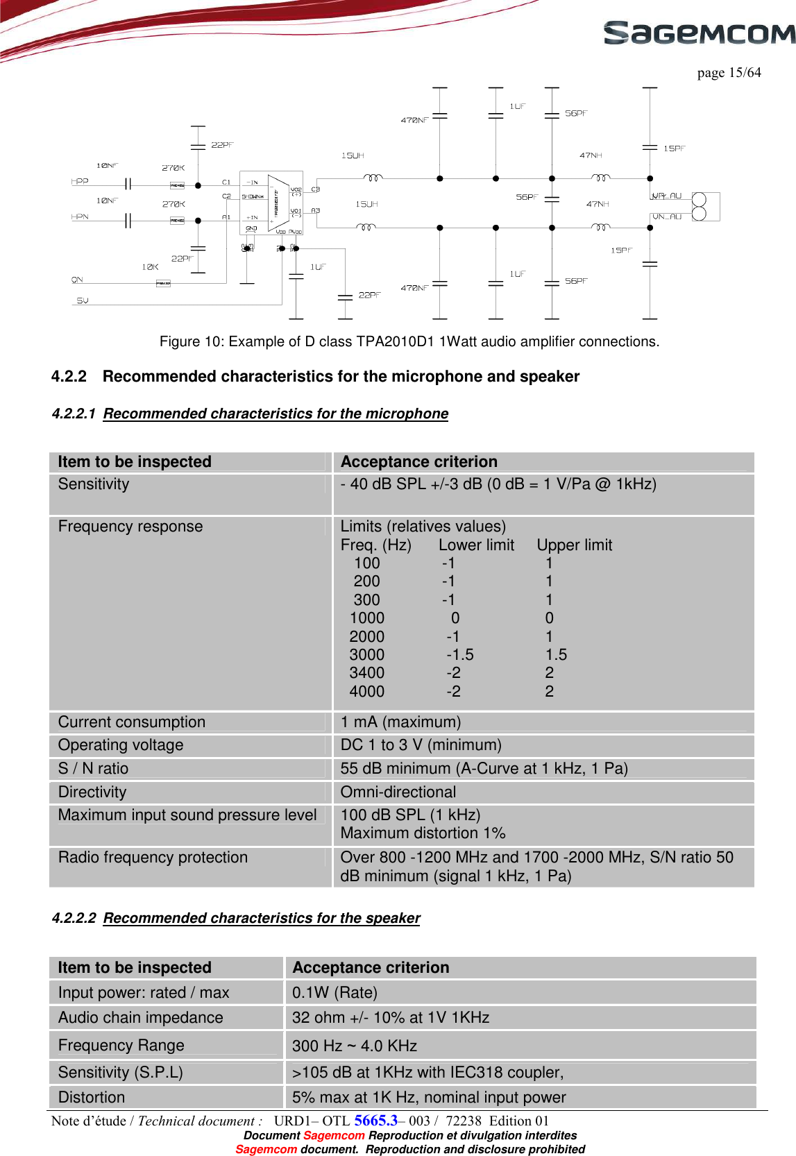
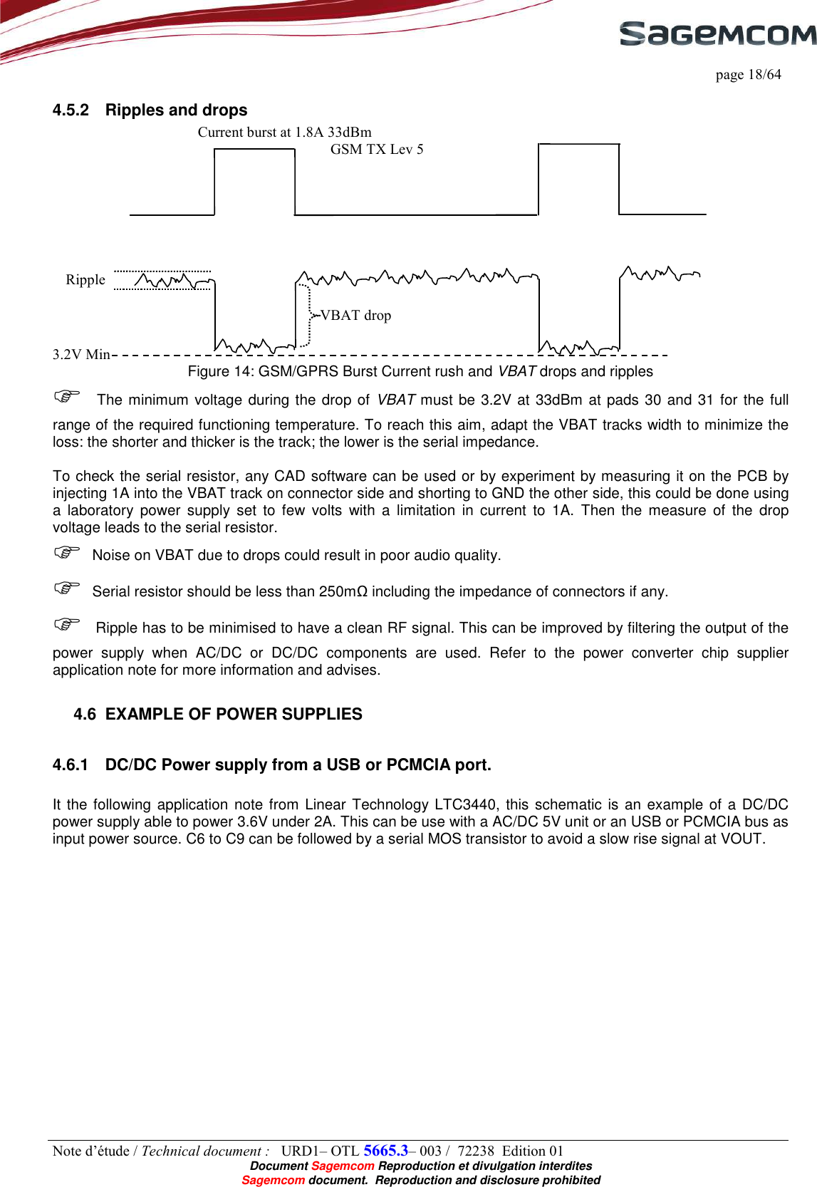
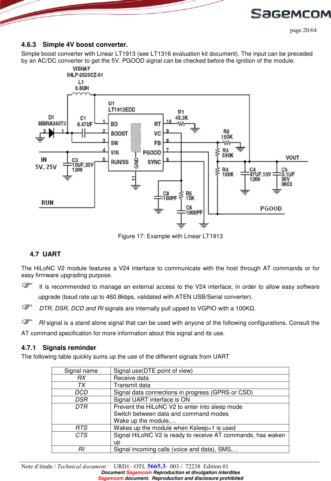
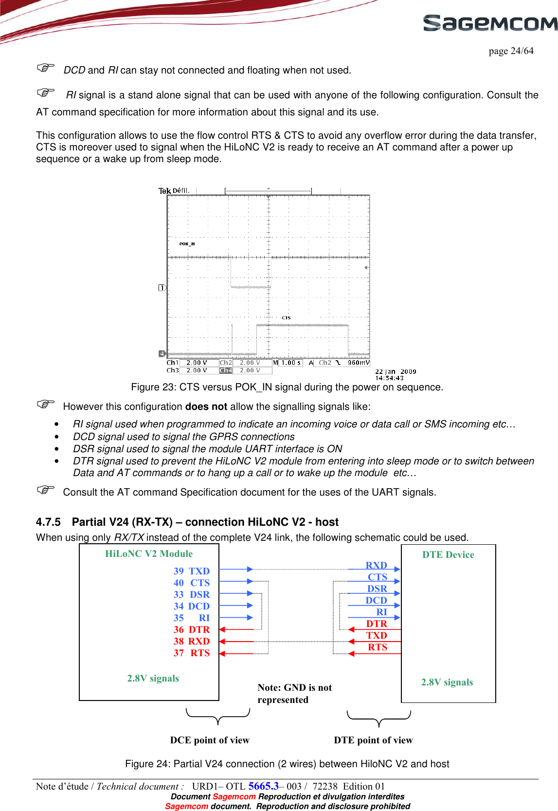
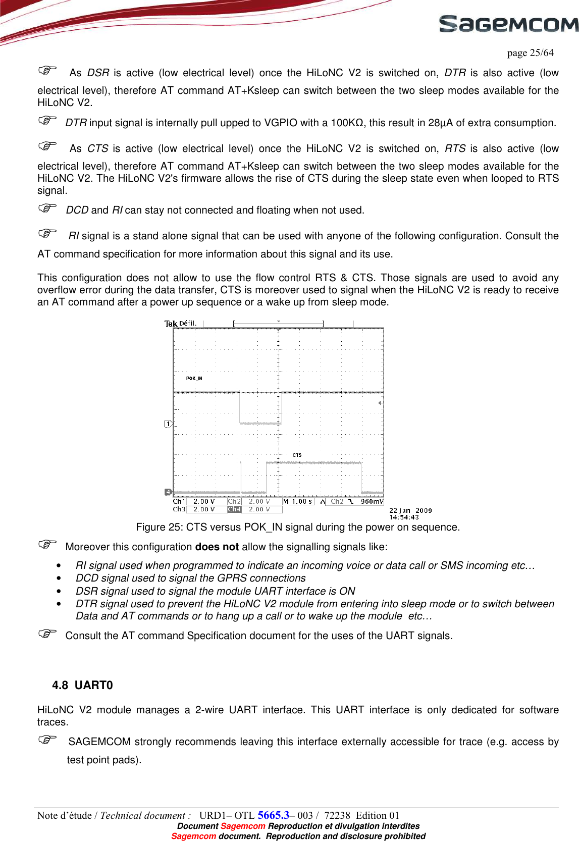
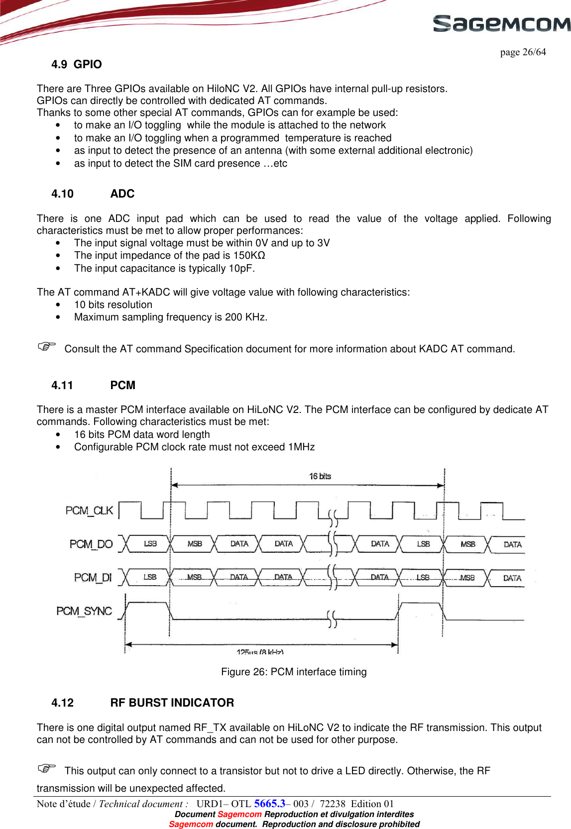
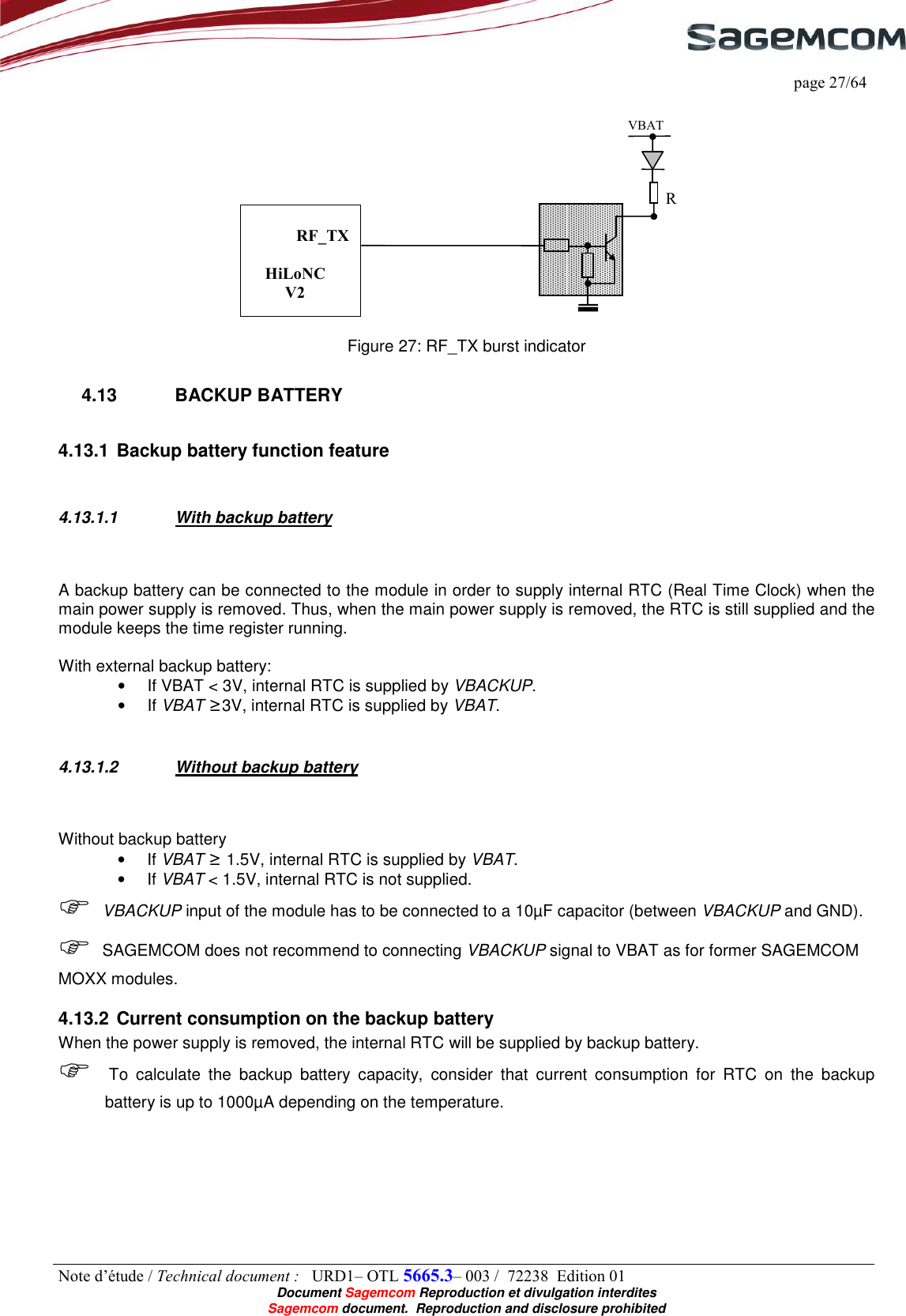
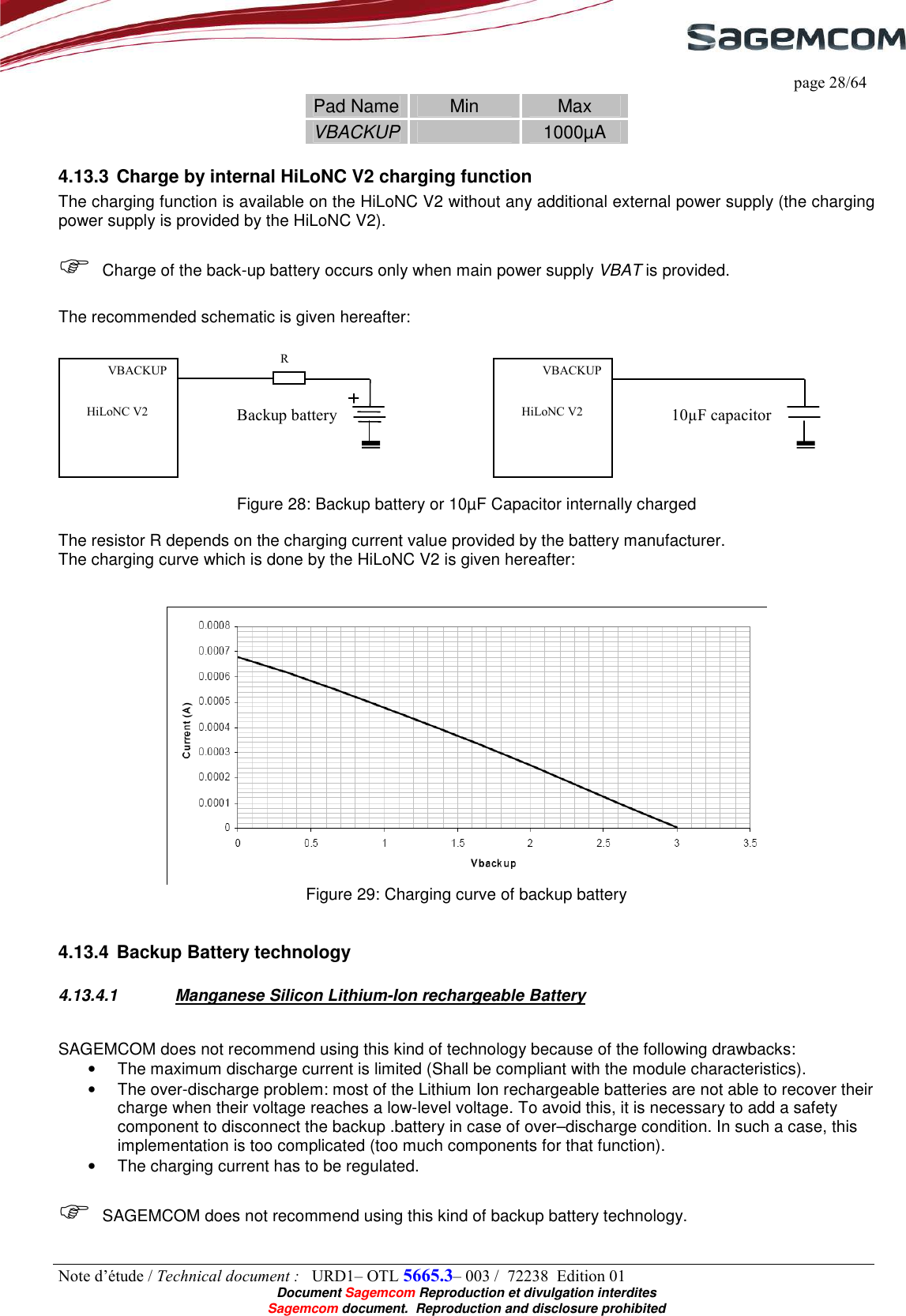
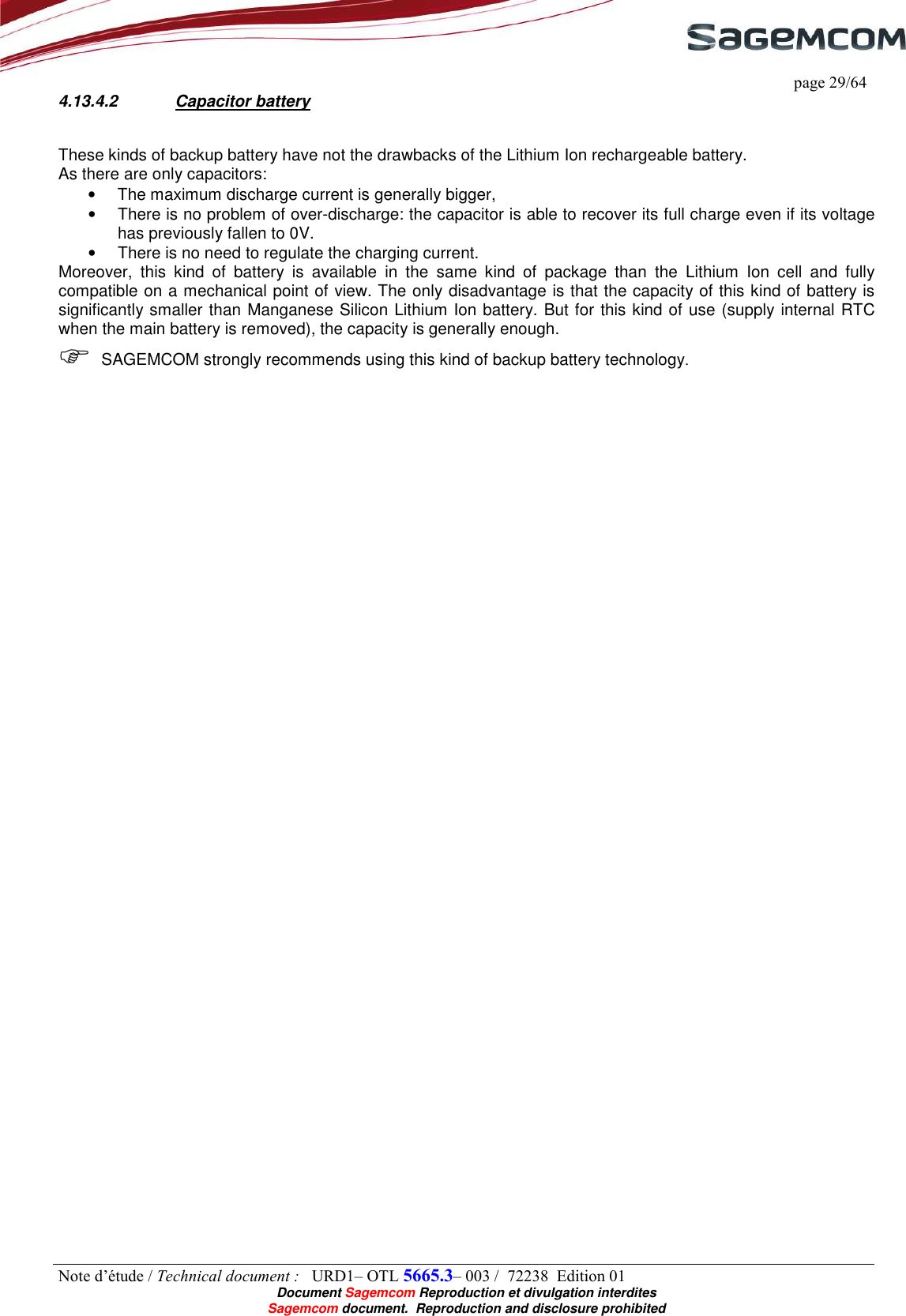
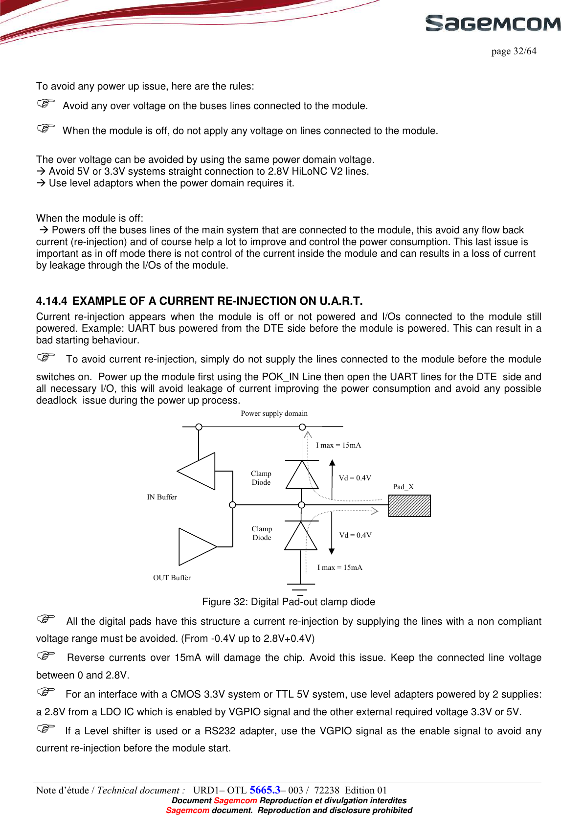
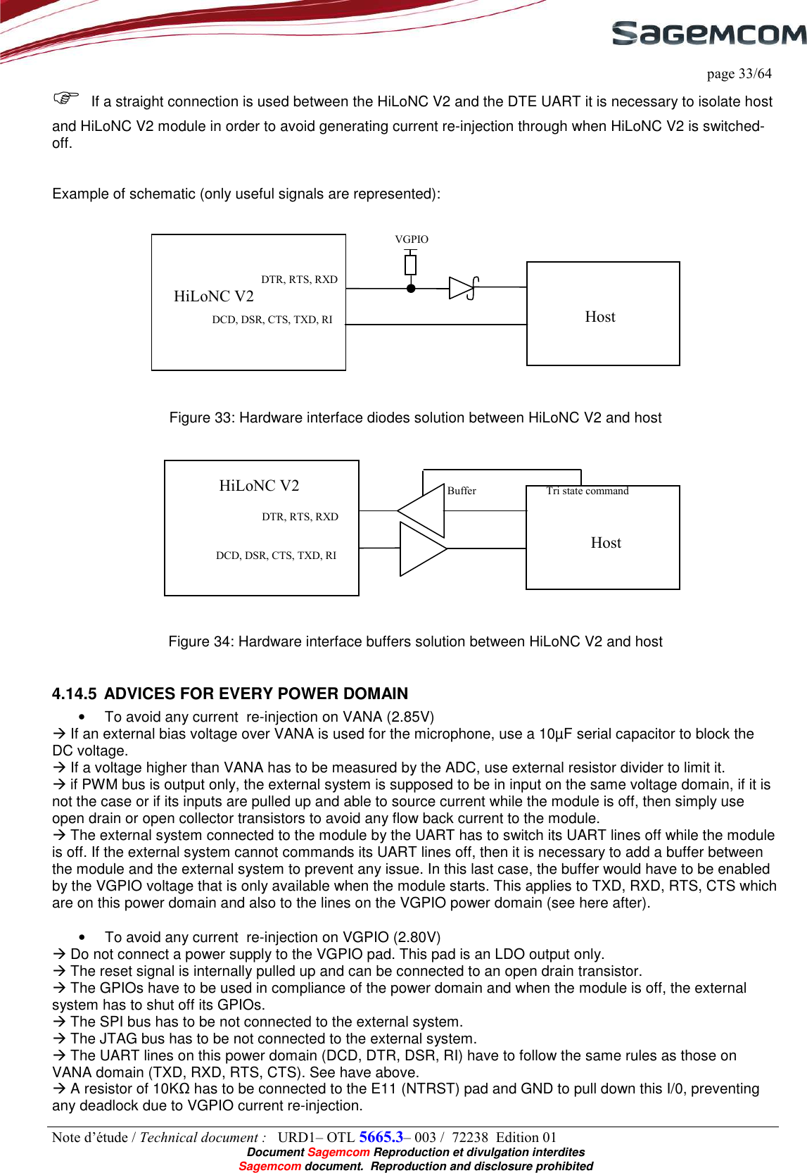
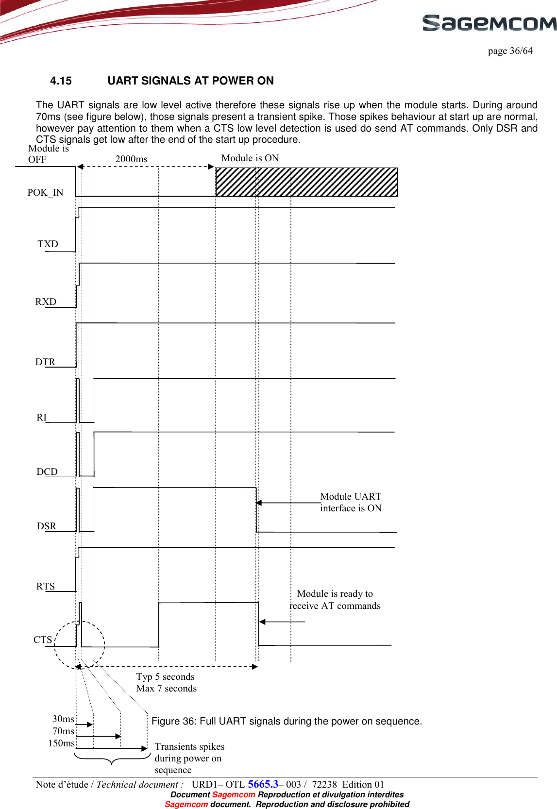
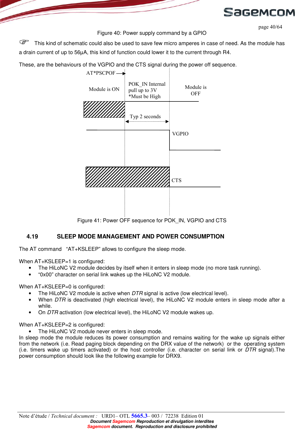
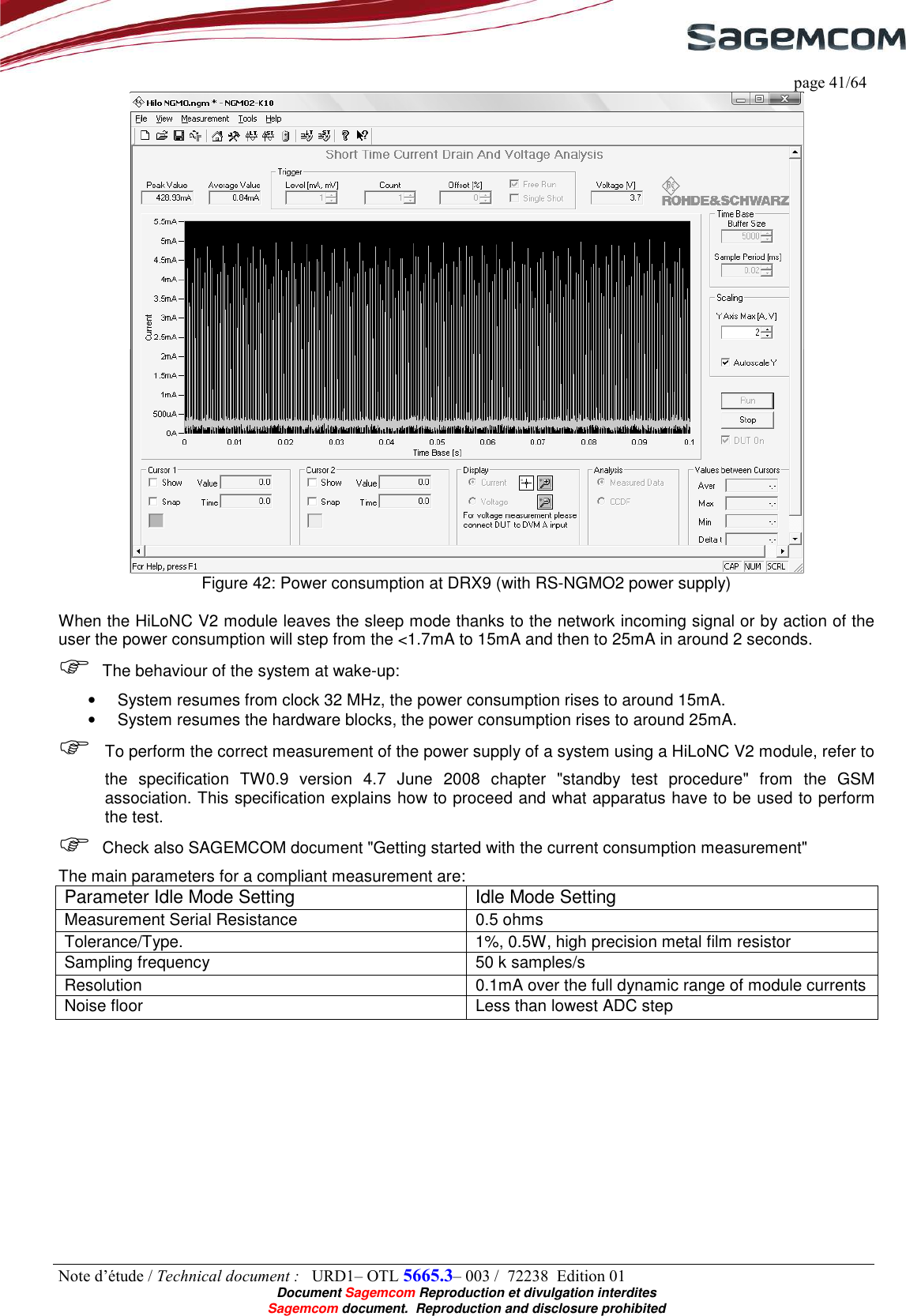
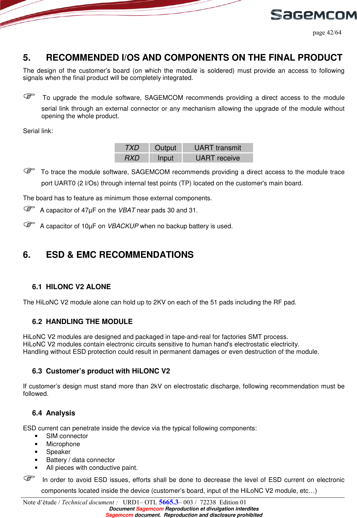
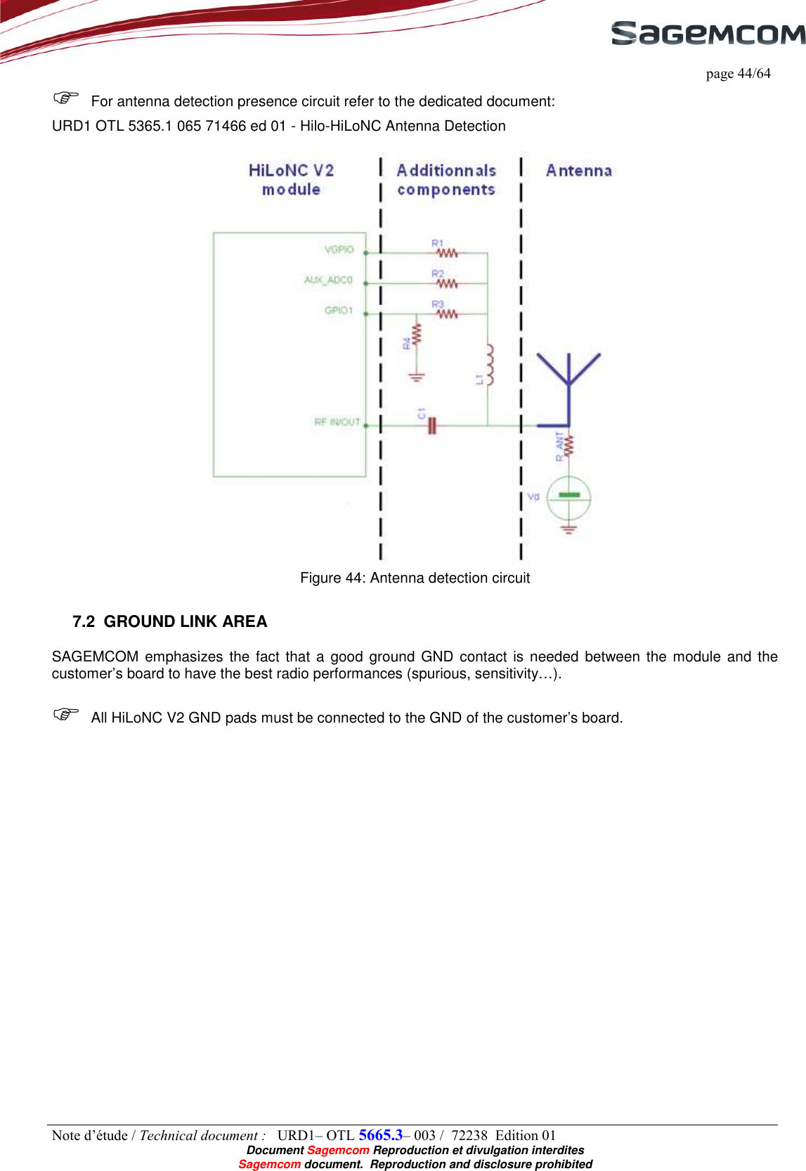
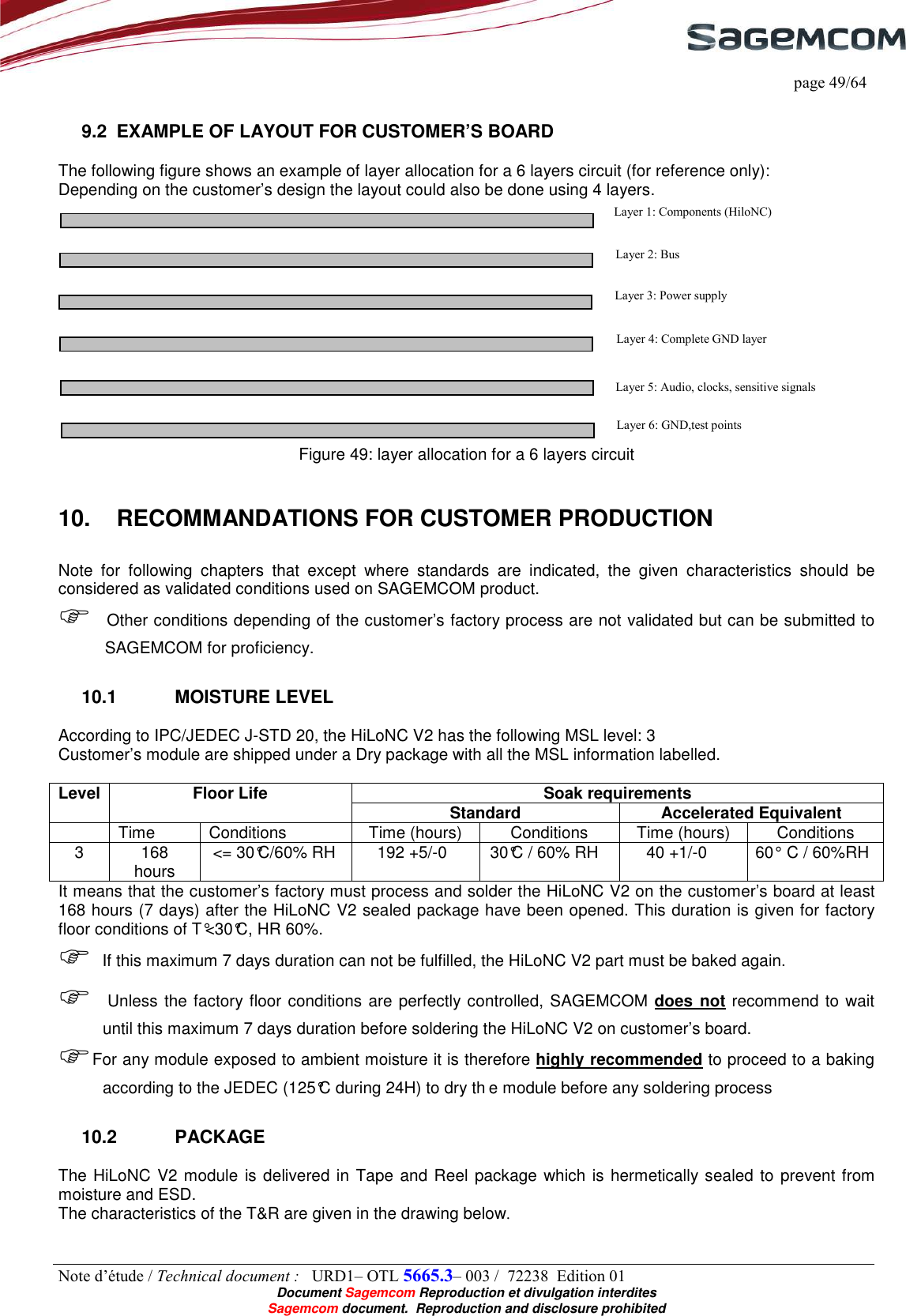
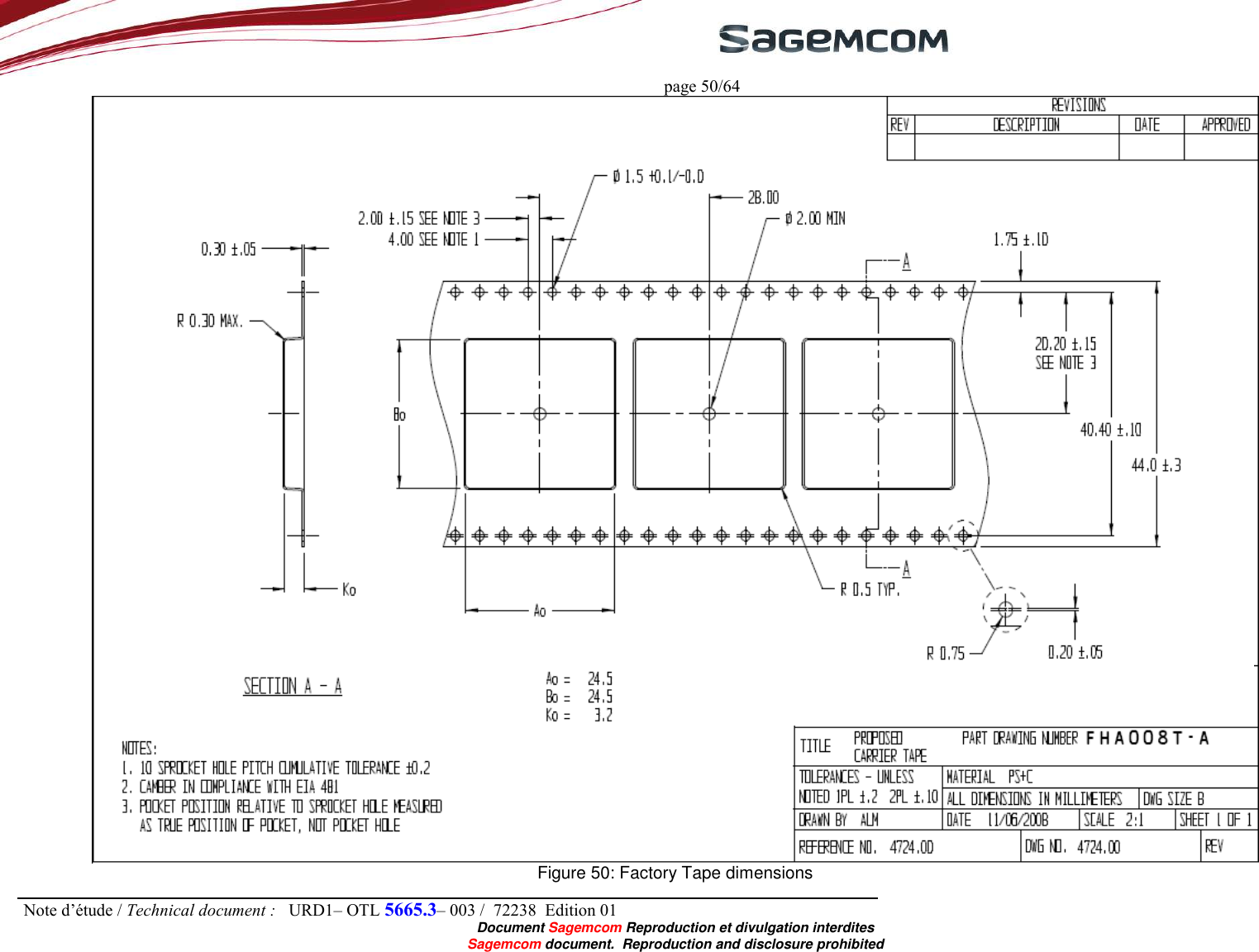
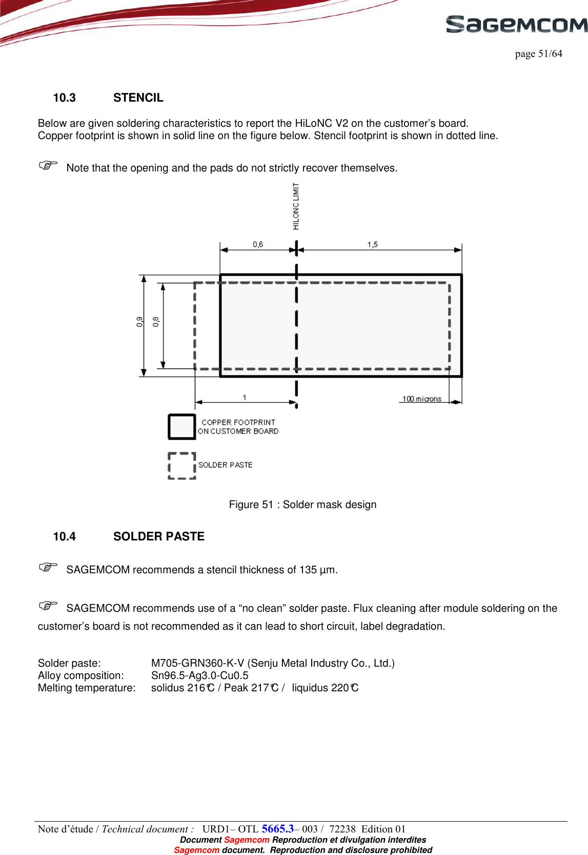
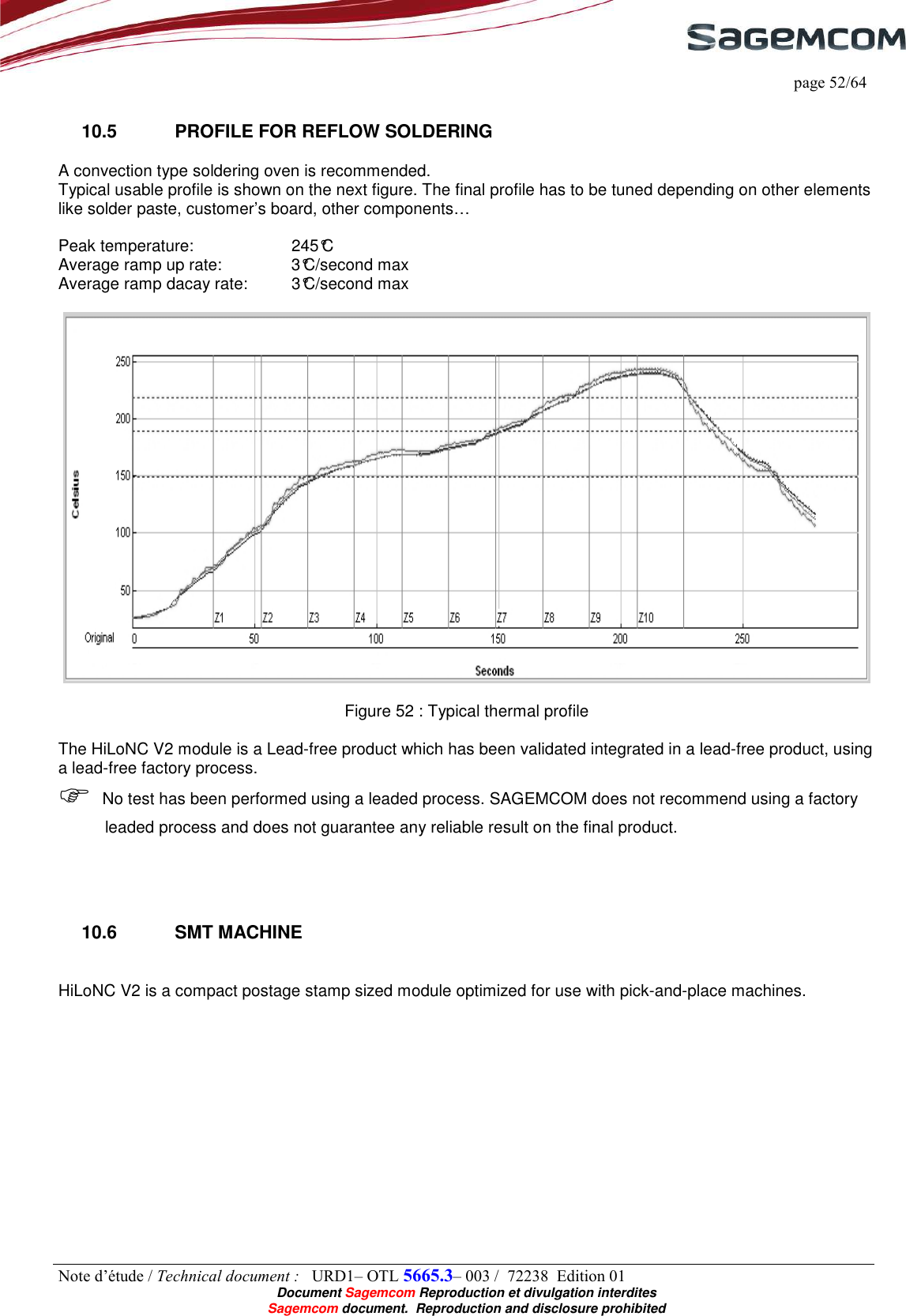
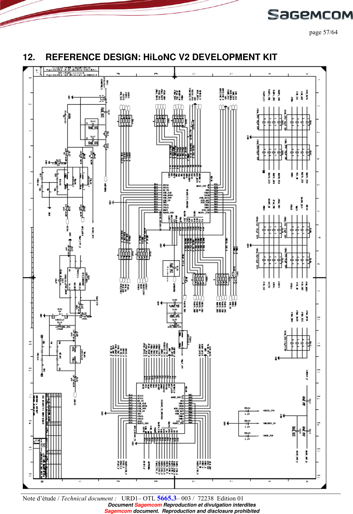
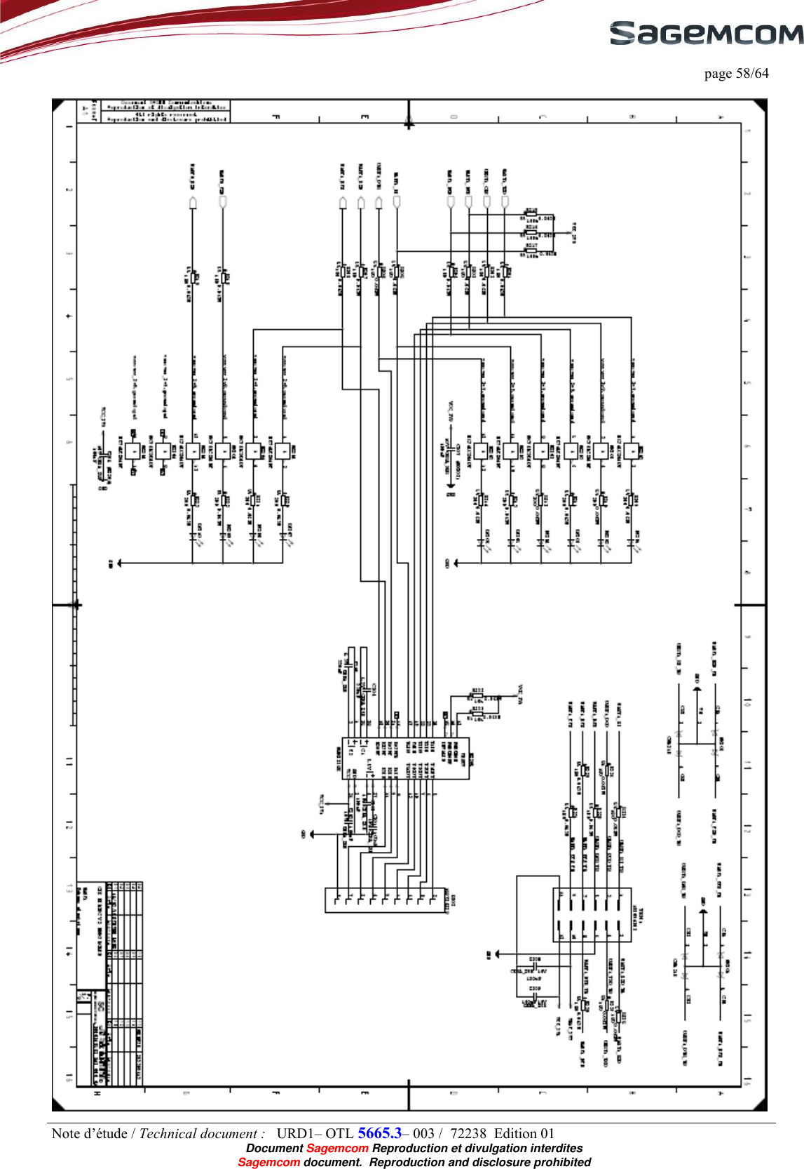
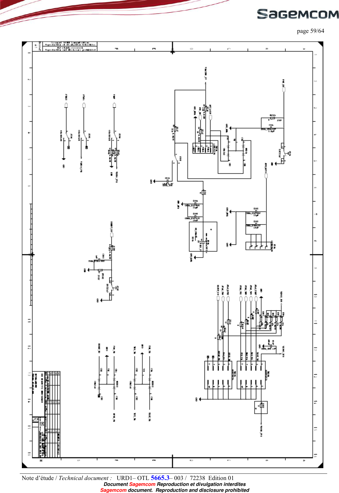
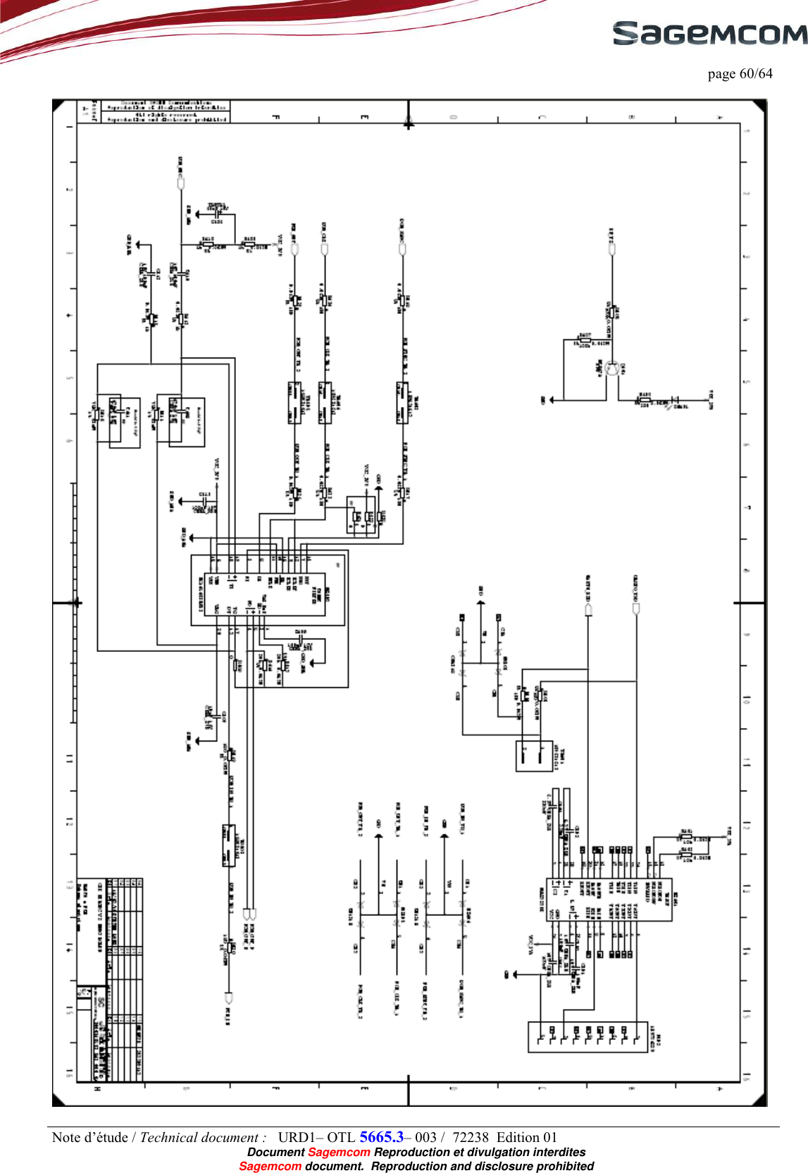
![page 19/64 Note d’étude / Technical document : URD1– OTL 5665.3– 003 / 72238 Edition 01 Document Sagemcom Reproduction et divulgation interdites Sagemcom document. Reproduction and disclosure prohibited Figure 15: Example of power supply based on a DC/DC step down converter 4.6.2 Simple high current low dropout voltage regulator. If the whole power consumption is not an issue, this example of a simple voltage regulator preceded by an AC/DC to 5V converter, can be use to power the module. Figure 16: Example of power supply based on regulator MIC29302WU The voltage output is given by: VOUT = 1.235V × [1 + (R1 / R2)] To have 3.7V out R1=560K & R2=271.8K (270K+1.8K)](https://usermanual.wiki/SAGEMCOM-BROANDS/HILONCV2/User-Guide-1376521-Page-17.png)