SAGEMCOM BROANDS HILONCV2 GPRS module User Manual
SAGEMCOM SAS GPRS module
User manual
page
3
/64
Note d’étude / Technical document : URD1– OTL
5665.3
– 003 / 72238 Edition 01
Document Sagemcom Reproduction et divulgation interdites
Sagemcom document. Reproduction and disclosure prohibited
HiLoNC V2 APPLICATION NOTE

page
4
/64
Note d’étude / Technical document : URD1– OTL
5665.3
– 003 / 72238 Edition 01
Document Sagemcom Reproduction et divulgation interdites
Sagemcom document. Reproduction and disclosure prohibited
SOMMAIRE / CONTENTS
1.
OVERVIEW...................................................................................................................................................................7
1.1
OBJECT OF THE DOCUMENT.........................................................................................................................7
1.2
REFERENCE DOCUMENTS.............................................................................................................................7
1.3
MODIFICATION OF THIS DOCUMENT ..........................................................................................................7
1.4
CONVENTIONS...................................................................................................................................................7
2.
BLOCK DIAGRAM.......................................................................................................................................................8
3.
HILONC FAMILY LEGACY........................................................................................................................................9
3.1
PADS OUT AND NEW FEATURES..................................................................................................................9
3.2
EASY MIGRATION FROM HILONC (V1) TO HILONC V2..........................................................................10
3.2.1
Migration without the use of new features..............................................................................................10
3.2.2
Migration with the use of new features ...................................................................................................10
4.
FUNCTIONAL INTEGRATION.................................................................................................................................10
4.1
HOW TO CONNECT TO A SIM CARD ..........................................................................................................11
4.2
HOW TO CONNECT THE AUDIOS? .............................................................................................................13
4.2.1
Connecting microphone and speaker .....................................................................................................13
4.2.2
Recommended characteristics for the microphone and speaker........................................................15
4.2.3
DTMF OVER GSM NETWORK ...............................................................................................................16
4.3
PWM ....................................................................................................................................................................16
4.3.1
PWM outputs ..............................................................................................................................................16
4.3.2
PWM for Buzzer connection.....................................................................................................................16
4.4
NETWORK LED.................................................................................................................................................17
4.5
POWER SUPPLY ..............................................................................................................................................17
4.5.1
Burst conditions..........................................................................................................................................17
4.5.2
Ripples and drops ......................................................................................................................................18
4.6
EXAMPLE OF POWER SUPPLIES................................................................................................................18
4.6.1
DC/DC Power supply from a USB or PCMCIA port..............................................................................18
4.6.2
Simple high current low dropout voltage regulator................................................................................19
4.6.3
Simple 4V boost converter. ......................................................................................................................20
4.7
UART ...................................................................................................................................................................20
4.7.1
Signals reminder ........................................................................................................................................20
4.7.2
Complete V24 – connection HiLoNC V2 - host .....................................................................................21
4.7.3
Complete V24 interface with PC..............................................................................................................22
4.7.4
Partial V24 (RX-TX-RTS-CTS) – connection HiLoNC V2 - host.........................................................23
4.7.5
Partial V24 (RX-TX) – connection HiLoNC V2 - host ...........................................................................24
4.8
UART0.................................................................................................................................................................25
4.9
GPIO ....................................................................................................................................................................26
4.10
ADC..................................................................................................................................................................26
4.11
PCM .................................................................................................................................................................26
4.12
RF BURST INDICATOR ...............................................................................................................................26
4.13
BACKUP BATTERY ......................................................................................................................................27
4.13.1
Backup battery function feature ...............................................................................................................27
4.13.2
Current consumption on the backup battery..........................................................................................27
4.13.3
Charge by internal HiLoNC V2 charging function .................................................................................28
4.13.4
Backup Battery technology.......................................................................................................................28
4.14
START THE MODULE PROPERLY AND AVOID POWER UP ISSUES..............................................30
4.14.1
Power domains...........................................................................................................................................30
4.14.2
IO DC PRESENCE BEFORE POWER ON. ..........................................................................................31
4.14.3
SIDE EFFECTS OF A RETRO SUPPLY (CURRENT RE-INJECTION) ...........................................31
4.14.4
EXAMPLE OF A CURRENT RE-INJECTION ON U.A.R.T. ................................................................32
4.14.5
ADVICES FOR EVERY POWER DOMAIN............................................................................................33
4.14.6
CASE OF VBAT RISE TIME ....................................................................................................................34
4.14.7
START- UP.................................................................................................................................................34
4.15
UART SIGNALS AT POWER ON................................................................................................................36
4.16
POWER ON AND SLEEP DIAGRAMS ......................................................................................................37
4.17
MODULE RESET...........................................................................................................................................39
4.18
MODULE SWITCH OFF ...............................................................................................................................39
4.19
SLEEP MODE MANAGEMENT AND POWER CONSUMPTION ..........................................................40

page
5
/64
Note d’étude / Technical document : URD1– OTL
5665.3
– 003 / 72238 Edition 01
Document Sagemcom Reproduction et divulgation interdites
Sagemcom document. Reproduction and disclosure prohibited
5.
RECOMMENDED I/OS AND COMPONENTS ON THE FINAL PRODUCT .........................................................42
6.
ESD & EMC RECOMMENDATIONS .......................................................................................................................42
6.1
HILONC V2 ALONE...........................................................................................................................................42
6.2
HANDLING THE MODULE ..............................................................................................................................42
6.3
Customer’s product with HiLONC V2..............................................................................................................42
6.4
Analysis ...............................................................................................................................................................42
6.5
Recommendations to avoid ESD issues ........................................................................................................43
7.
RADIO INTEGRATION..............................................................................................................................................43
7.1
ANTENNA ...........................................................................................................................................................43
7.2
GROUND LINK AREA.......................................................................................................................................44
7.3
LAYOUT ..............................................................................................................................................................45
7.4
MECHANICAL SURROUNDING.....................................................................................................................46
7.5
OTHER RECOMMENDATIONS – TESTS FOR PRODUCTION/DESIGN ...............................................46
8.
AUDIO INTEGRATION .............................................................................................................................................46
8.1
MECHANICAL INTEGRATION AND ACOUSTICS......................................................................................46
8.2
ELECTRONICS AND LAYOUT .......................................................................................................................47
9.
RECOMMENDATIONS ON LAYOUT OF CUSTOMER’S BOARD ......................................................................47
9.1
GENERAL RECOMMENDATIONS ON LAYOUT.........................................................................................47
9.1.1
Ground.........................................................................................................................................................47
9.1.2
Power supplies ...........................................................................................................................................47
9.1.3
Clocks ..........................................................................................................................................................48
9.1.4
Data bus and other signals.......................................................................................................................48
9.1.5
Radio............................................................................................................................................................48
9.1.6
Audio............................................................................................................................................................48
9.2
EXAMPLE OF LAYOUT FOR CUSTOMER’S BOARD................................................................................49
10.
RECOMMANDATIONS FOR CUSTOMER PRODUCTION ...............................................................................49
10.1
MOISTURE LEVEL........................................................................................................................................49
10.2
PACKAGE.......................................................................................................................................................49
10.3
STENCIL .........................................................................................................................................................51
10.4
SOLDER PASTE............................................................................................................................................51
10.5
PROFILE FOR REFLOW SOLDERING.....................................................................................................52
10.6
SMT MACHINE ..............................................................................................................................................52
10.6.1
Nozzles........................................................................................................................................................53
10.6.2
Fiducials ......................................................................................................................................................54
10.7
UNDERFILL....................................................................................................................................................54
10.8
SECOND REFLOW SOLDERING...............................................................................................................55
10.9
HAND SOLDERING ......................................................................................................................................55
10.10
UNSOLDERING.............................................................................................................................................55
11.
LABEL .....................................................................................................................................................................56
12.
REFERENCE DESIGN: HiLoNC V2 DEVELOPMENT KIT................................................................................57

page
6
/64
Note d’étude / Technical document : URD1– OTL
5665.3
– 003 / 72238 Edition 01
Document Sagemcom Reproduction et divulgation interdites
Sagemcom document. Reproduction and disclosure prohibited
FIGURES LIST
Figure 1: Block diagram of HiLoNC module ...........................................................................................................................8
Figure 2: Postage stamp sized HiLoNC V2 51 pads out front side ........................................................................................11
Figure 3: Postage stamp sized HiLoNC V2 51 pads out back side.........................................................................................11
Figure 4: SIM Card signals.....................................................................................................................................................11
Figure 5: Protections: EMC and ESD components close to the SIM .....................................................................................12
Figure 6: Protections: Serial resistors for long SIM bus lines. ...............................................................................................12
Figure 7: Audio connection ....................................................................................................................................................13
Figure 8 : Filter and ESD protection of microphone ..............................................................................................................14
Figure 9: Filter and ESD protection of 32 ohms speaker........................................................................................................14
Figure 10: Example of D class TPA2010D1 1Watt audio amplifier connections. .................................................................15
Figure 11: Buzzer connection.................................................................................................................................................16
Figure 12: Network LED connection .....................................................................................................................................17
Figure 13: GSM/GPRS Burst Current rush ............................................................................................................................17
Figure 14: GSM/GPRS Burst Current rush and VBAT drops and ripples...............................................................................18
Figure 15: Example of power supply based on a DC/DC step down converter......................................................................19
Figure 16: Example of power supply based on regulator MIC29302WU ..............................................................................19
Figure 17: Example with Linear LT1913 ...............................................................................................................................20
Figure 18: Complete V24 connection between HiLoNC V2 and host....................................................................................21
Figure 19: CTS versus POK_IN signal during the power on sequence. .................................................................................21
Figure 20: connection to a data cable .....................................................................................................................................22
Figure 21: Example of a connection to a data cable with a MAX3238E................................................................................23
Figure 22: Partial V24 connection (4 wires) between HiLoNC V2 and host .........................................................................23
Figure 23: CTS versus POK_IN signal during the power on sequence. .................................................................................24
Figure 24: Partial V24 connection (2 wires) between HiloNC V2 and host...........................................................................24
Figure 25: CTS versus POK_IN signal during the power on sequence. .................................................................................25
Figure 26: PCM interface timing............................................................................................................................................26
Figure 27: RF_TX burst indicator ..........................................................................................................................................27
Figure 28: Backup battery or 10µF Capacitor internally charged ..........................................................................................28
Figure 29: Charging curve of backup battery .........................................................................................................................28
Figure 30 : HiLoNC V2 51 pads with their power domains...................................................................................................30
Figure 31 : HiLoNC V2 51 pads with their power domains…continued ...............................................................................31
Figure 32: Digital Pad-out clamp diode..................................................................................................................................32
Figure 33: Hardware interface diodes solution between HiLoNC V2 and host......................................................................33
Figure 34: Hardware interface buffers solution between HiLoNC V2 and host.....................................................................33
Figure 35: Power ON sequence ..............................................................................................................................................35
Figure 36: Full UART signals during the power on sequence................................................................................................36
Figure 37: Diagram for the power on .....................................................................................................................................37
Figure 38: Diagram for the sleep mode ..................................................................................................................................38
Figure 39: Reset command of the HiLoNC V2 by an external GPIO ....................................................................................39
Figure 40: Power supply command by a GPIO ......................................................................................................................40
Figure 41: Power OFF sequence for POK_IN, VGPIO and CTS...........................................................................................40
Figure 42: Power consumption at DRX9 (with RS-NGMO2 power supply) .........................................................................41
Figure 43: Antenna connection...............................................................................................................................................43
Figure 44: Antenna detection circuit ......................................................................................................................................44
Figure 45: Mandatory area for varnish ...................................................................................................................................45
Figure 46: Connection of RF lines with different width.........................................................................................................45
Figure 47: Layout of audio differential signals on a layer n...................................................................................................48
Figure 48: Adjacent layers of audio differential signals .........................................................................................................48
Figure 49: layer allocation for a 6 layers circuit.....................................................................................................................49
Figure 50: Factory Tape dimensions ......................................................................................................................................50
Figure 51 : Solder mask design ..............................................................................................................................................51
Figure 52 : Typical thermal profile.........................................................................................................................................52
Figure 53 : Flexjet nozzle 340F..............................................................................................................................................53
Figure 54 : Siemens nozzle 417..............................................................................................................................................53
Figure 55 : Fiducials positions................................................................................................................................................54
Figure 56 : Underfill injection holes.......................................................................................................................................55
Figure 57 : Laboratory hot plate to unsolder the module........................................................................................................56

page
7
/64
Note d’étude / Technical document : URD1– OTL
5665.3
– 003 / 72238 Edition 01
Document Sagemcom Reproduction et divulgation interdites
Sagemcom document. Reproduction and disclosure prohibited
1. OVERVIEW
1.1 OBJECT OF THE DOCUMENT
The aim of this document is to describe some examples of hardware solutions for developing products around
the SAGEMCOM HiLoNC V2 GPRS Module. Most parts of these solutions are not mandatory. Use them as
suggestions of what should be done to have a working product and what should be avoided thanks to our
experiences.
This document suggests how to integrate the HiLoNC V2 GPRS module in machine devices such as
automotive, AMM (Automatic Metering Management), tracking system: connection with external devices, layout
advises, external components (decoupling capacitors…).
1.2 REFERENCE DOCUMENTS
URD1 OTL 5665.3 001 71927 - HiLoNC V2 technical specification
URD1 OTL 5635.1 008 70248 - AT Command Set for SAGEM HiLo Modules
1.3 MODIFICATION OF THIS DOCUMENT
The information presented in this document is supposed to be accurate and reliable. SAGEMCOM assumes no
responsibility for its use, nor any infringement of patents or other rights of third parties which may result from its
use.
This document is subject to change without notice.
Changes or modifications not expressly approved by the party responsible for compliance could void the user’s
authority to operate the equipment.
1.4 CONVENTIONS
SIGNAL NAME: All signal names available on the pads of the HiLoNC V2 module is written in italic.
Specific attention must be granted to the information given here.
page 8/64
Note d’étude / Technical document : URD1– OTL
5665.3
– 003 / 72238 Edition 01
Document Sagemcom Reproduction et divulgation interdites
Sagemcom document. Reproduction and disclosure prohibited
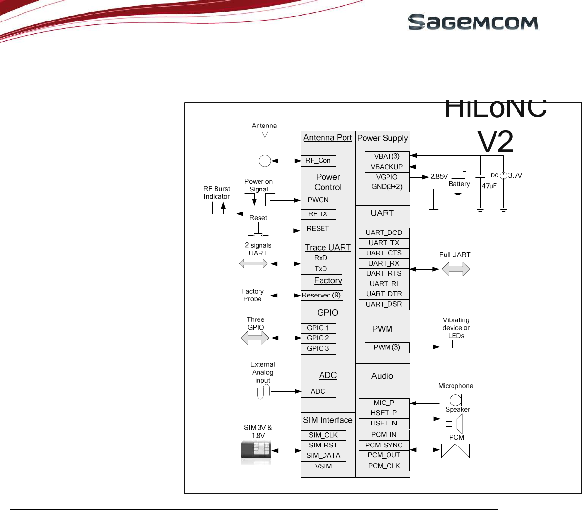
2. BLOCK DIAGRAM
Figure 1: Block diagram of HiLoNC module
page 9/64
Note d’étude / Technical document : URD1– OTL
5665.3
– 003 / 72238 Edition 01
Document Sagemcom Reproduction et divulgation interdites
Sagemcom document. Reproduction and disclosure prohibited
3. HILONC FAMILY LEGACY
3.1 PADS OUT AND NEW FEATURES
HiLoNC Pads HiLoNC V2
Signal Name
HiLoNC V2
Function
HiLoNC V1
Signal Name
HiLoNC V1
Function Delta
E1 /INTMIC_P AUDIO /INTMIC_P AUDIO P2P Compliant
E2 /AUX_ADC0 ADC /AUX_ADC0 ADC P2P Compliant
E3 GND POWER GND POWER P2P Compliant
E4 VGPIO EXT_VDD VGPIO EXT_VDD P2P Compliant
E5 VBACKUP EXT_VDD VBACKUP EXT_VDD P2P Compliant
E6 /PWM0 PWM /PWM0 PWM P2P Compliant
E7 /RESET_IN RESET /RESET_IN RESET P2P Compliant
E8 SAGEMCOM FACTORY USE SAGEMCOM FACTORY P2P Compliant
E9 SAGEMCOM FACTORY USE SAGEMCOM FACTORY P2P Compliant
E10 SAGEMCOM FACTORY USE SAGEMCOM FACTORY P2P Compliant
E11 NTRST JTAG/FACTORY /JTAG_TRST JTAG P2P Compliant
E12 SAGEMCOM FACTORY USE SAGEMCOM FACTORY P2P Compliant
E13 SAGEMCOM FACTORY USE SAGEMCOM FACTORY P2P Compliant
E14 /GPIO2 GPIO /GPIO2 GPIO P2P Compliant
E15 /GPIO1 GPIO /GPIO1 GPIO P2P Compliant
E16 /RF_TX RF /GPIO8_SPI_IN SPI New Feature
E17 /PCM_CLK PCM /SCL_SPI_OUT SPI New Feature
E18 /PCM_SYNC PCM /SDA_SPI_SEL SPI New Feature
E19 /PCM_OUT PCM /GPIO6_SPI_IRQ SPI New Feature
E20 /PCM_IN PCM /GPIO7_SPI_CLK SPI New Feature
E21 GND POWER GND POWER P2P Compliant
E22 / JTAG1 JTAG /TEST_GPIO1 GPIO P2P Compliant
E23 /JTAG2 JTAG /TEST_GPIO2 GPIO P2P Compliant
E24 /TEST JTAG /TEST JTAG P2P Compliant
E25 /UART0_RXD Trace UART 0 /GPIO4 GPIO New Feature
E26 /GPIO3 GPIO /GPIO3 GPIO P2P Compliant
E27 GND RF GND RF P2P Compliant
E28 /ANTENNA RF /ANTENNA RF P2P Compliant
E29 GND RF GND RF P2P Compliant
E30 VBATT POWER VBATT POWER P2P Compliant
E31 VBATT POWER VBATT POWER P2P Compliant
E32 /UART0_TXD Trace UART 0 /GPIO5 GPIO New Feature
E33 /UART1_DSR UART 1 /UART1_DSR UART P2P Compliant
E34 /UART1_DCD UART 1 /UART1_DCD UART P2P Compliant
E35 /UART1_RI UART 1 /UART1_RI UART P2P Compliant
E36 /UART1_DTR UART 1 /UART1_DTR UART P2P Compliant
E37 /UART1_RTS UART 1 /UART1_RTS UART P2P Compliant
E38 /UART1_RX UART 1 /UART1_RX UART P2P Compliant
E39 /UART1_TX UART 1 /UART1_TX UART P2P Compliant
E40 /UART1_CTS UART 1 /UART1_CTS UART P2P Compliant
E41 /POK_IN POWER ON /POK_IN POWER ON P2P Compliant
E42 /PWM2 PWM /PWM2 PWM P2P Compliant
E43 /PWM1 PWM /PWM1 PWM P2P Compliant
E44 /SIM_CLK SIM /SIM_CLK SIM P2P Compliant

page 10/64
Note d’étude / Technical document : URD1– OTL
5665.3
– 003 / 72238 Edition 01
Document Sagemcom Reproduction et divulgation interdites
Sagemcom document. Reproduction and disclosure prohibited
E45 /SIM_RST SIM /SIM_RST SIM P2P Compliant
E46 /SIM_DATA SIM /SIM_DATA SIM P2P Compliant
E47 VSIM SIM VSIM SIM P2P Compliant
E48 VBATT POWER VBATT POWER P2P Compliant
E49 GND POWER GND POWER P2P Compliant
E50 /HSET_OUT_P AUDIO /HSET_OUT_P AUDIO P2P Compliant
E51 /HSET_OUT_N AUDIO /HSET_OUT_N AUDIO P2P Compliant
As seen in the table above, the two modules are almost pad to pad (P2P) compliant for the main important signals, however
the new HiLoNC V2 M2M module introduce some new interesting features as the digital audio on the PCM bus and the RF
bust indicator signal.
3.2 EASY MIGRATION FROM HILONC (V1) TO HILONC V2
3.2.1 Migration without the use of new features
When upgrading from the HiLoNC V1 to the HiLoNC V2, the SPI bus formerly used was supposed to be left as test points
on your design, then simply left the design as it is, therefore the new PCM bus and RF burst indicator signals will remain
not used.
For the former GPIO4 and GPIO5, if there were both not used, simply add if possible two test points on those signals to be
able to connect a trace cable in case of need. Otherwise, if one or both former GPIO4 and GPIO5 were used, you have to
reallocate those pads to GPIO1, GPIO2 or GPIO3 which remain pad to pad compliant.
3.2.2 Migration with the use of new features
When upgrading from the HiLoNC V1 to the HiLoNC V2, the former SPI bus which was supposed to be left on test points
is now used as the digital audio PCM bus and also the RF indicator signal, simply connect the new signals as described
below in the respective chapter.
The former GPIO4 and GPIO5 signals are now used to connect the UART TXD / RXD trace bus, then add if possible two
test points on those signals to be able to connect a trace cable in case of need.
4. FUNCTIONAL INTEGRATION
The improvement of Silicon technologies heads toward functionality improvement, less power consumption. The
postage stamp sized HiLoNC V2 module meets all these requirement, uses the last high end technology in a
very compact design of only 24 x 24 x 2.6 mm and weighs less than 3 grams.
All digital I/Os among the 51 pads are in 2.8V domain which is suitable for most systems except SIM I/O's
with can also be in the 1.8V domain depending on the used SIM card and POK_IN at 3Vdomain
Analogical I/Os are in the following power domains
• VSIM (the SIM I/Os at 1.8V or 2.9V domain).
• VBACKUP 3V domain
• VGPIO 2.8V domain
• VBAT (from 3.2V to 4.5V domain)
• AUX_ADC0 2.8V domain
• INTMIC_P 2.85V domain
• HSET_OUT_P/N VBAT domain
• ANTENNA (RF power Amplifier is on VBAT domain)
Do not power the module I/O with a voltage over the specified limits, this could damage the module.
Acoustic engineering competences are mandatory to get accurate audio performance on customer’s
product
Radio engineering competences are mandatory to get accurate radio performance on customer’s product.
page 11/64
Note d’étude / Technical document : URD1– OTL
5665.3
– 003 / 72238 Edition 01
Document Sagemcom Reproduction et divulgation interdites
Sagemcom document. Reproduction and disclosure prohibited
Figure 2: Postage stamp sized HiLoNC V2 51 pads out front side
Figure 3: Postage stamp sized HiLoNC V2 51 pads out back side
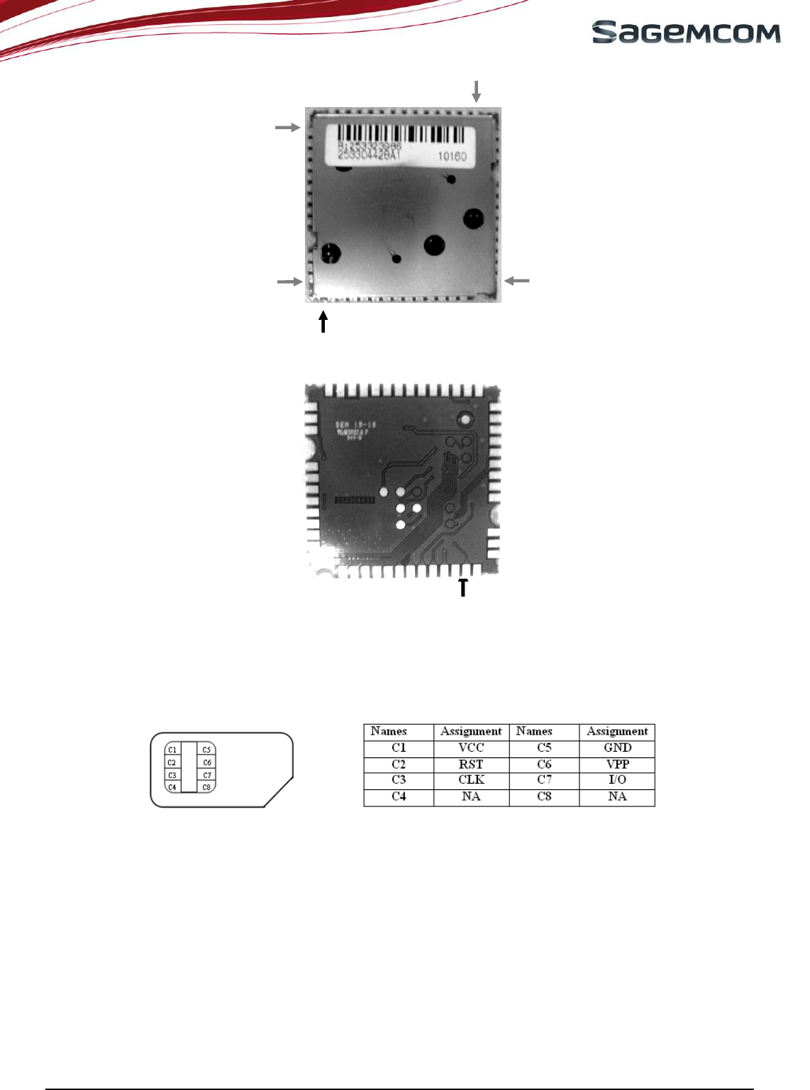
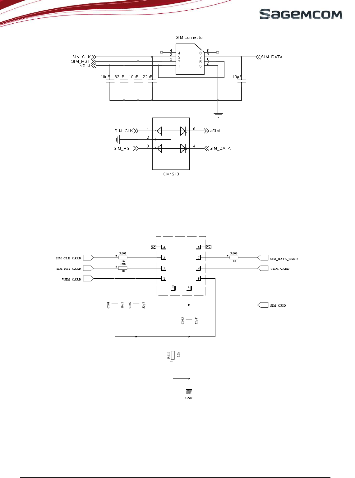
4.1 HOW TO CONNECT TO A SIM CARD
Figure 4: SIM Card signals
HiLoNC V2 module provides the SIM signals on the 51 pads. A SIM card holder with 6 pads needs to be
adopted to use the SIM function.
Decoupling capacitors have to be added on SIM_CLK, SIM_RST, VSIM and SIM_DATA signals as close
as possible to the SIM card connector to avoid EMC issues and pass the SIM card tests approvals .
Use ESD protection components to protect SIM card and module I/Os against Electro Static Discharges.
The following schematic shows how to protect the SIM access for 6 pads connector, this should be apply
every time a SIM card holder is accessible by the final customer.
1
51
14
26
40
1
page 12/64
Note d’étude / Technical document : URD1– OTL
5665.3
– 003 / 72238 Edition 01
Document Sagemcom Reproduction et divulgation interdites
Sagemcom document. Reproduction and disclosure prohibited
Figure 5: Protections: EMC and ESD components close to the SIM
In case of long SIM bus lines over 10cm, it is recommended to also use serial resistors to avoid electrical
overshoots on SIM bus signals. Use 56Ω for the clock line and 10Ω for the reset and data lines.
Figure 6: Protections: Serial resistors for long SIM bus lines.
The schematic here above includes the hardware SIM card presence detector. It can be connected to any GPIO
and managed with an AT command.
SIM card must not be removed from its holder while it is still powered. First switch the module off properly
with the AT command, then remove the SIM card from its holder.
page 13/64
Note d’étude / Technical document : URD1– OTL
5665.3
– 003 / 72238 Edition 01
Document Sagemcom Reproduction et divulgation interdites
Sagemcom document. Reproduction and disclosure prohibited
4.2 HOW TO CONNECT THE AUDIOS?
The HiLoNC V2 module features one input audio path and one output audio path. The input path is single-end
while the output path is differential. In this following chapter examples of design will be given including
protections against EMC and ESD and some notes about the routing rules to follow to avoid the TDMA noise
sometimes present in this sensitive area of design.
Note that acoustic engineering competences are mandatory to get accurate audio performance on
customer’s product.
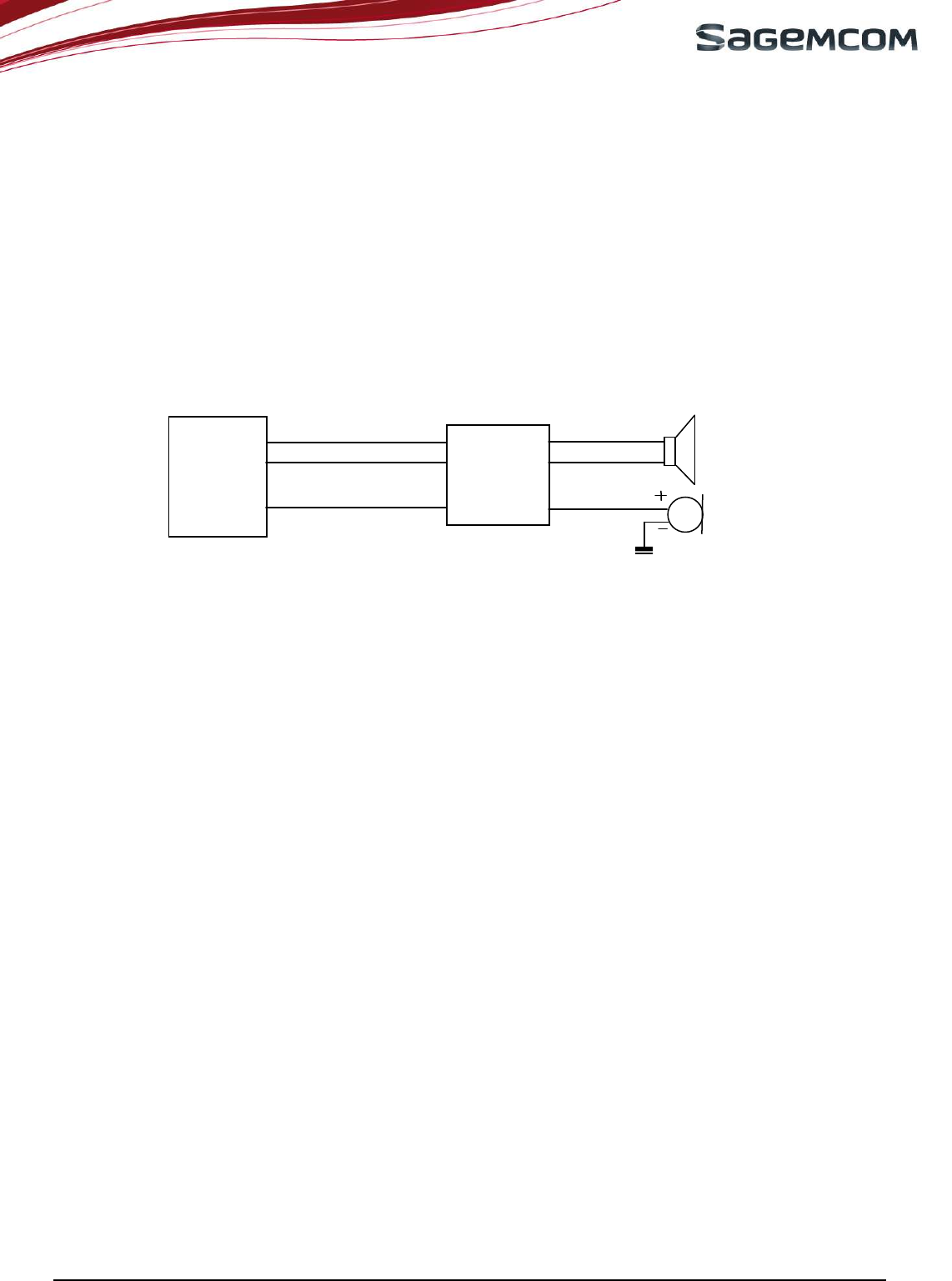
4.2.1 Connecting microphone and speaker
The HiLoNC V2 module can manage an external microphone (INTMIC_P) in single-end mode and an external
speaker (HSET_OUT_P / HSET_OUT_N) in differential mode. Thus, one speaker and one microphone can be
connected to the module. The 2.4V voltage to bias the microphone is implemented in the module.
The speaker connected to the module should be 32 ohms.
Figure 7: Audio connection
If the design is ESD or EMC sensitive we strongly recommend reading the notes below.
A poor audio quality could either come from the PCB routing and placement or from the chosen components (or
even both).
HiLoNC
V2
Filter and
ESD
protection
HSET_OUT_P
HSET_OUT_N
INTMIC_P
32ohms speaker
MIC
page 14/64
Note d’étude / Technical document : URD1– OTL
5665.3
– 003 / 72238 Edition 01
Document Sagemcom Reproduction et divulgation interdites
Sagemcom document. Reproduction and disclosure prohibited
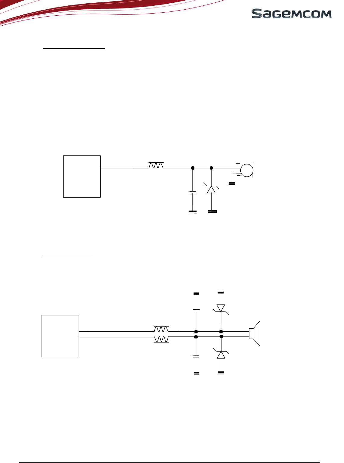
4.2.1.1 Notes for microphone
Pay attention to the microphone device, it must not be sensitive to RF disturbances.
If you need to have deported microphone out of the board with long wires, you should pay attention to the
EMC and ESD effect. It is also the case when your design is ESD sensitive. In those cases, add the
following protections to improve your design.
To ensure proper operation of such sensitive signals, they have to be isolated from the others by
analogue ground on customer’s board layout. (Refer to Layout design chapter)
Figure 8 : Filter and ESD protection of microphone
To use an external bias voltage for the microphone, simply use a capacitor of 10µF to prevent this bias
voltage to be re-injected inside the module.
4.2.1.2 Notes for speaker
As explained for the microphone, if the speaker is deported out of the board or is sensitive to ESD, use the
schematic here after to improve the audio.
Figure 9: Filter and ESD protection of 32 ohms speaker
HSET_OUT_P, HSET_OUT_N tracks must be larger than other tracks: 0.1 mm.
As described in the layout chapter, differential signals have to be routed in parallel (HSET_OUT_P and
HSET_OUT_N signals)
The impedance of audio chain (filter + speaker) must be lower than 32Ω.
To use an external audio amplifier connected to a loud-speaker, use serial capacitors of 10nF on HiLoNC
audio outputs to connect the audio amplifier.
HiLoNC V2
INTMIC_P
MIC
Ferrite Bead
18pF
ESD protection
HiLoNC V2
HSET_OUT_P
HSET_OUT_N
speaker
Ferrite Bead
Ferrite Bead
18pF
18pF
ESD protection
ESD protection
page 15/64
Note d’étude / Technical document : URD1– OTL
5665.3
– 003 / 72238 Edition 01
Document Sagemcom Reproduction et divulgation interdites
Sagemcom document. Reproduction and disclosure prohibited
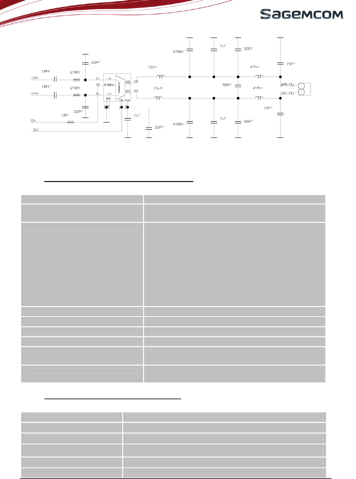
Figure 10: Example of D class TPA2010D1 1Watt audio amplifier connections.
4.2.2 Recommended characteristics for the microphone and speaker
4.2.2.1 Recommended characteristics for the microphone
Item to be inspected Acceptance criterion
Sensitivity - 40 dB SPL +/-3 dB (0 dB = 1 V/Pa @ 1kHz)
Frequency response Limits (relatives values)
Freq. (Hz) Lower limit Upper limit
100 -1 1
200 -1 1
300 -1 1
1000 0 0
2000 -1 1
3000 -1.5 1.5
3400 -2 2
4000 -2 2
Current consumption 1 mA (maximum)
Operating voltage DC 1 to 3 V (minimum)
S / N ratio 55 dB minimum (A-Curve at 1 kHz, 1 Pa)
Directivity Omni-directional
Maximum input sound pressure level 100 dB SPL (1 kHz)
Maximum distortion 1%
Radio frequency protection Over 800 -1200 MHz and 1700 -2000 MHz, S/N ratio 50
dB minimum (signal 1 kHz, 1 Pa)
4.2.2.2 Recommended characteristics for the speaker
Item to be inspected Acceptance criterion
Input power: rated / max 0.1W (Rate)
Audio chain impedance 32 ohm +/- 10% at 1V 1KHz
Frequency Range 300 Hz ~ 4.0 KHz
Sensitivity (S.P.L) >105 dB at 1KHz with IEC318 coupler,
Distortion 5% max at 1K Hz, nominal input power
page 16/64
Note d’étude / Technical document : URD1– OTL
5665.3
– 003 / 72238 Edition 01
Document Sagemcom Reproduction et divulgation interdites
Sagemcom document. Reproduction and disclosure prohibited
4.2.3 DTMF OVER GSM NETWORK
Former systems used to transmits data through DTMF modulation on RTC telephone lines.
Audio DTMF tones are not guarantee over GSM network
This is due to the nature of the GSM Voice CODEC - it is specifically designed for the human voice and does
not faithfully transmit DTMF.
When you press the buttons on your GSM handset during a call, this goes in the Signalling channel - it does not
generate in-band DTMF; the actual DTMF tones are generated in the network.
Therefore if your design needs the DTMF functionality, you should know their transmission over the network is
not at all guaranteed (because of voice codec). This could work or fail depending very strongly to the GSM
network provider. SAGEMCOM does not guarantee any success on using this function.
However tests on HiLoNC V2 shown this feature can work on some GSM Networks. Successful transmissions
and receptions have been done with 300ms of characters duration and 200mVpp as input level on microphone
input.
If this function is needed, first try with your network and those parameters then (if success) try to tune
them to fit your specification.
4.3 PWM
4.3.1 PWM outputs
The HiLoNC V2 module can manage two PWM outputs.
They can be configured with appropriate AT command (for more details refer to AT command set for
SAGEMCOM HiLoNC V2 module specification).
User application can set for each output:
• Frequency between : 25.6KHz and 1083.3KHz
• Duty range from: 0 to 100%
4.3.2 PWM for Buzzer connection
The HiLoNC V2 module can manage a dedicate PWM output to drive a buzzer. The buzzer can be used to
alarm for abnormal state.
Resistors should be added to protect the buzzer. The value of these resistors depends on the buzzer and
the transistor. Normally, they can be set as 1KΩ.
Figure 11: Buzzer connection
R1
R2
HiloNC
VBAT
PWM2
page 17/64
Note d’étude / Technical document : URD1– OTL
5665.3
– 003 / 72238 Edition 01
Document Sagemcom Reproduction et divulgation interdites
Sagemcom document. Reproduction and disclosure prohibited
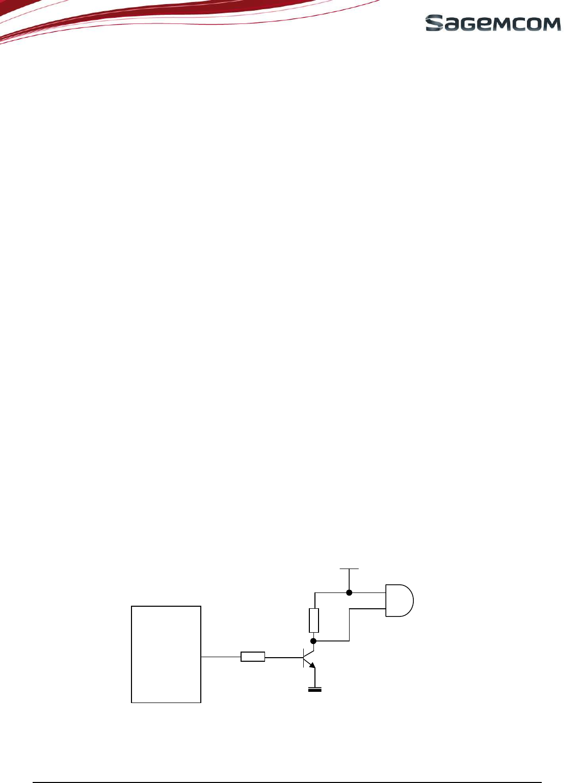
4.4 NETWORK LED
The HiLoNC V2 module can manage a network LED. The LED can be connected either to one of the available
GPIO or to a PWM (but not the one dedicated to the buzzer).
The transistors can be found a in a single package referenced as UMDXX or PUMDXX Family.
Value of resistor R depends on characteristic of chosen LED; it is used to limit the current through the diode.
Use the AT command to set the GPIO or PWM used to control the LED.
Figure 12: Network LED connection
4.5 POWER SUPPLY
The HiLoNC V2 module can be supplied by a battery or any DC/DC converter compliant with the module supply
range 3.2V to 4.5V and 2.2 A.
The PCB tracks must be well dimensioned to support 2.2 A maximum current (Burst current 1.8A plus the
extra current for the other used I/Os). The voltage ripple caused by serial resistance of power supply path
(Battery internal resistance, tracks and contact resistance) could result in the voltage drops.
To prevent any issue in the power up procedure the typical rise time for VBAT should be 1ms.
The HiLoNC V2 module does not manage the battery charging.
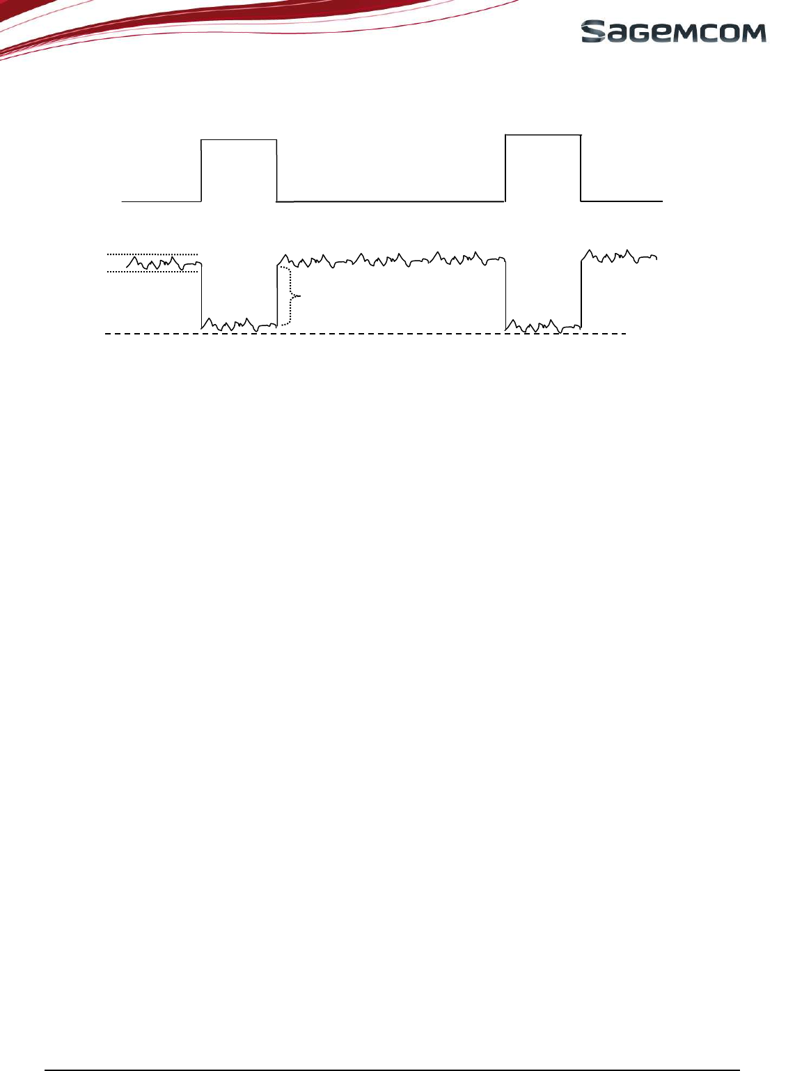
4.5.1 Burst conditions
- Communication mode (worst case: 2 continuous GSM time-slot pulse):
Figure 13: GSM/GPRS Burst Current rush
A 47µF with Low ESR capacitor is highly recommended for VBAT and close to the module pads 30 & 31.
GPIO or
PWM
HiLoNC V2
VBAT
R
page 18/64
Note d’étude / Technical document : URD1– OTL
5665.3
– 003 / 72238 Edition 01
Document Sagemcom Reproduction et divulgation interdites
Sagemcom document. Reproduction and disclosure prohibited
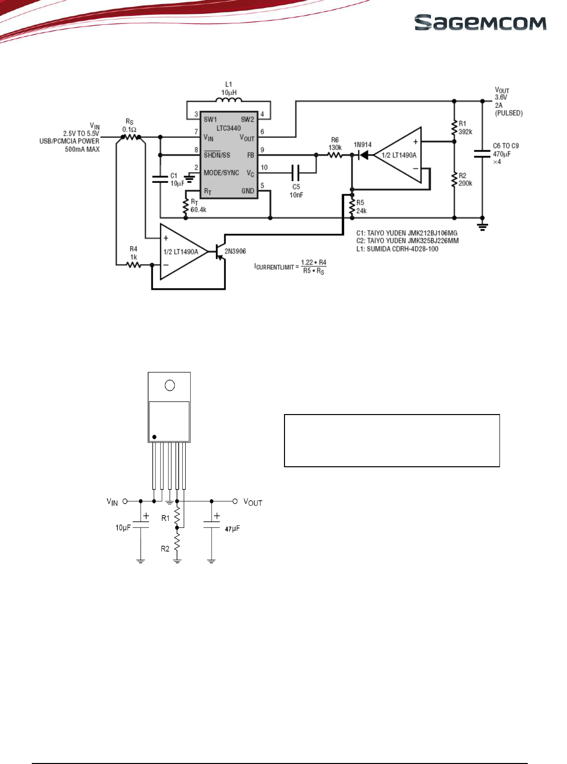
4.5.2 Ripples and drops
Figure 14: GSM/GPRS Burst Current rush and VBAT drops and ripples
The minimum voltage during the drop of VBAT must be 3.2V at 33dBm at pads 30 and 31 for the full
range of the required functioning temperature. To reach this aim, adapt the VBAT tracks width to minimize the
loss: the shorter and thicker is the track; the lower is the serial impedance.
To check the serial resistor, any CAD software can be used or by experiment by measuring it on the PCB by
injecting 1A into the VBAT track on connector side and shorting to GND the other side, this could be done using
a laboratory power supply set to few volts with a limitation in current to 1A. Then the measure of the drop
voltage leads to the serial resistor.
Noise on VBAT due to drops could result in poor audio quality.
Serial resistor should be less than 250mΩ including the impedance of connectors if any.
Ripple has to be minimised to have a clean RF signal. This can be improved by filtering the output of the
power supply when AC/DC or DC/DC components are used. Refer to the power converter chip supplier
application note for more information and advises.
4.6 EXAMPLE OF POWER SUPPLIES
4.6.1 DC/DC Power supply from a USB or PCMCIA port.
It the following application note from Linear Technology LTC3440, this schematic is an example of a DC/DC
power supply able to power 3.6V under 2A. This can be use with a AC/DC 5V unit or an USB or PCMCIA bus as
input power source. C6 to C9 can be followed by a serial MOS transistor to avoid a slow rise signal at VOUT.
3.2V Min
Ripple
VBAT drop
Current burst at 1.8A 33dBm
GSM TX Lev 5
page 19/64
Note d’étude / Technical document : URD1– OTL
5665.3
– 003 / 72238 Edition 01
Document Sagemcom Reproduction et divulgation interdites
Sagemcom document. Reproduction and disclosure prohibited
Figure 15: Example of power supply based on a DC/DC step down converter
4.6.2 Simple high current low dropout voltage regulator.
If the whole power consumption is not an issue, this example of a simple voltage regulator preceded by an
AC/DC to 5V converter, can be use to power the module.
Figure 16: Example of power supply based on regulator MIC29302WU
The voltage output is given by:
VOUT = 1.235V × [1 + (R1 / R2)]
To have 3.7V out R1=560K & R2=271.8K
(270K+1.8K)
page 20/64
Note d’étude / Technical document : URD1– OTL
5665.3
– 003 / 72238 Edition 01
Document Sagemcom Reproduction et divulgation interdites
Sagemcom document. Reproduction and disclosure prohibited
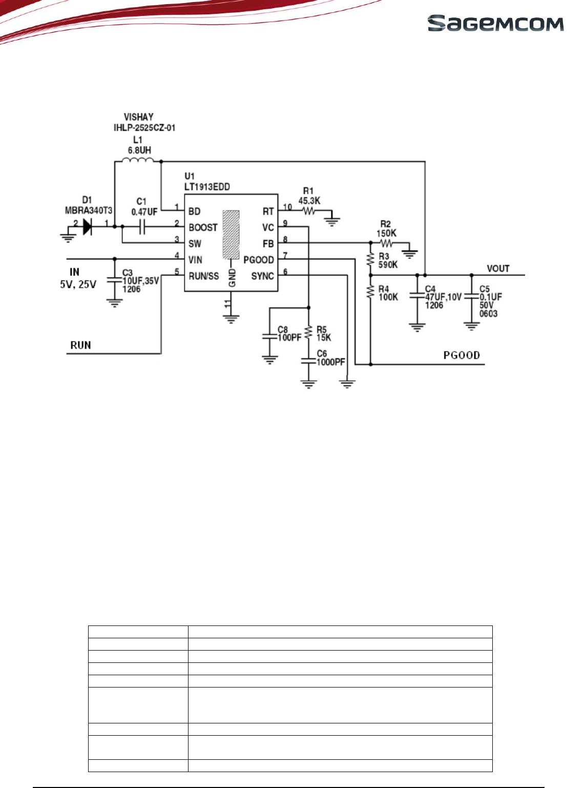
4.6.3 Simple 4V boost converter.
Simple boost converter with Linear LT1913 (see LT1316 evaluation kit document). The input can be preceded
by an AC/DC converter to get the 5V. PGOOD signal can be checked before the ignition of the module.
Figure 17: Example with Linear LT1913
4.7 UART
The HiLoNC V2 module features a V24 interface to communicate with the host through AT commands or for
easy firmware upgrading purpose.
It is recommended to manage an external access to the V24 interface, in order to allow easy software
upgrade (baud rate up to 460.8kbps, validated with ATEN USB/Serial converter).
DTR, DSR, DCD and RI signals are internally pull upped to VGPIO with a 100KΩ.
RI signal is a stand alone signal that can be used with anyone of the following configurations. Consult the
AT command specification for more information about this signal and its use.
4.7.1 Signals reminder
The following table quickly sums up the use of the different signals from UART
Signal name Signal use(DTE point of view)
RX Receive data
TX Transmit data
DCD Signal data connections in progress (GPRS or CSD)
DSR Signal UART interface is ON
DTR Prevent the HiLoNC V2 to enter into sleep mode
Switch between data and command modes
Wake up the module,…
RTS Wakes up the module when Ksleep=1 is used
CTS Signal HiLoNC V2 is ready to receive AT commands, has waken
up
RI Signal incoming calls (voice and data), SMS,…
page 21/64
Note d’étude / Technical document : URD1– OTL
5665.3
– 003 / 72238 Edition 01
Document Sagemcom Reproduction et divulgation interdites
Sagemcom document. Reproduction and disclosure prohibited
Consult the AT command Specification document for the use of the UART signals.
Unused signals can be left not connected.
4.7.2 Complete V24 – connection HiLoNC V2 - host
A V24 interface is provided on the 51 pads of the HiLoNC V2 module with the following signals: RTS/CTS,
RXD/TXD, DSR, DTR, DCD, RI.
The use of this complete V24 connection is recommended as soon as your application needs to exchange
data (over GPRS or CSD).
Figure 18: Complete V24 connection between HiLoNC V2 and host
This configuration allows to use the flow control RTS & CTS to avoid any overflow error during the data transfer,
CTS is moreover used to signal when the HiLoNC V2 is ready to receive an AT command after a power up
sequence or a wake up from sleep mode.
This configuration allows as well all the signalling signals like:
• RI signal used when programmed to indicate an incoming voice or data call or SMS incoming etc…
• DCD signal used to signal the GPRS connections
• DSR signal used to signal the module UART interface is ON
• DTR signal used to prevent the HiLoNC V2 module from entering into sleep mode or to switch between
Data and AT commands or to hang up a call or to wake up the module etc…
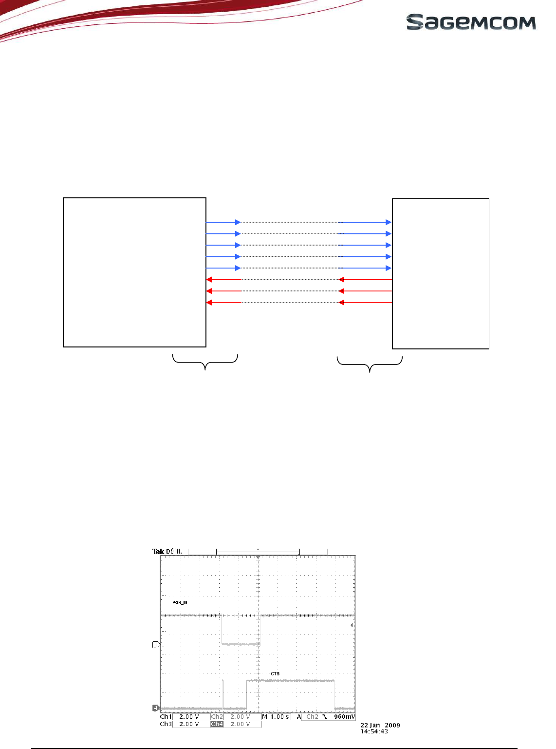
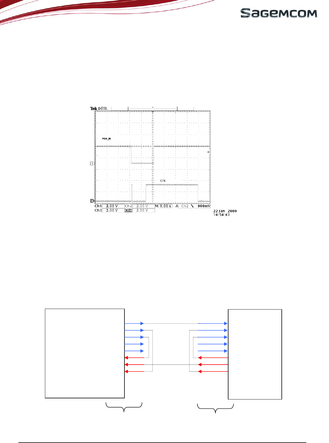
Figure 19: CTS versus POK_IN signal during the power on sequence.
DCE point of view DTE point of view
RXD
CTS
DSR
DCD
RI
DTR
TXD
RTS
HiLoNC V2 Module
TXD
CTS
DSR
DCD
RI
DTR
RXD
RTS
DTE Device
2.8V signals
39
40
33
34
35
36
38
37
2.8V signals
Note: GND is not
represented
page 22/64
Note d’étude / Technical document : URD1– OTL
5665.3
– 003 / 72238 Edition 01
Document Sagemcom Reproduction et divulgation interdites
Sagemcom document. Reproduction and disclosure prohibited
Avoid supplying the UART before the HiLoNC V2 module is ON, this could result in bad power up
sequence.
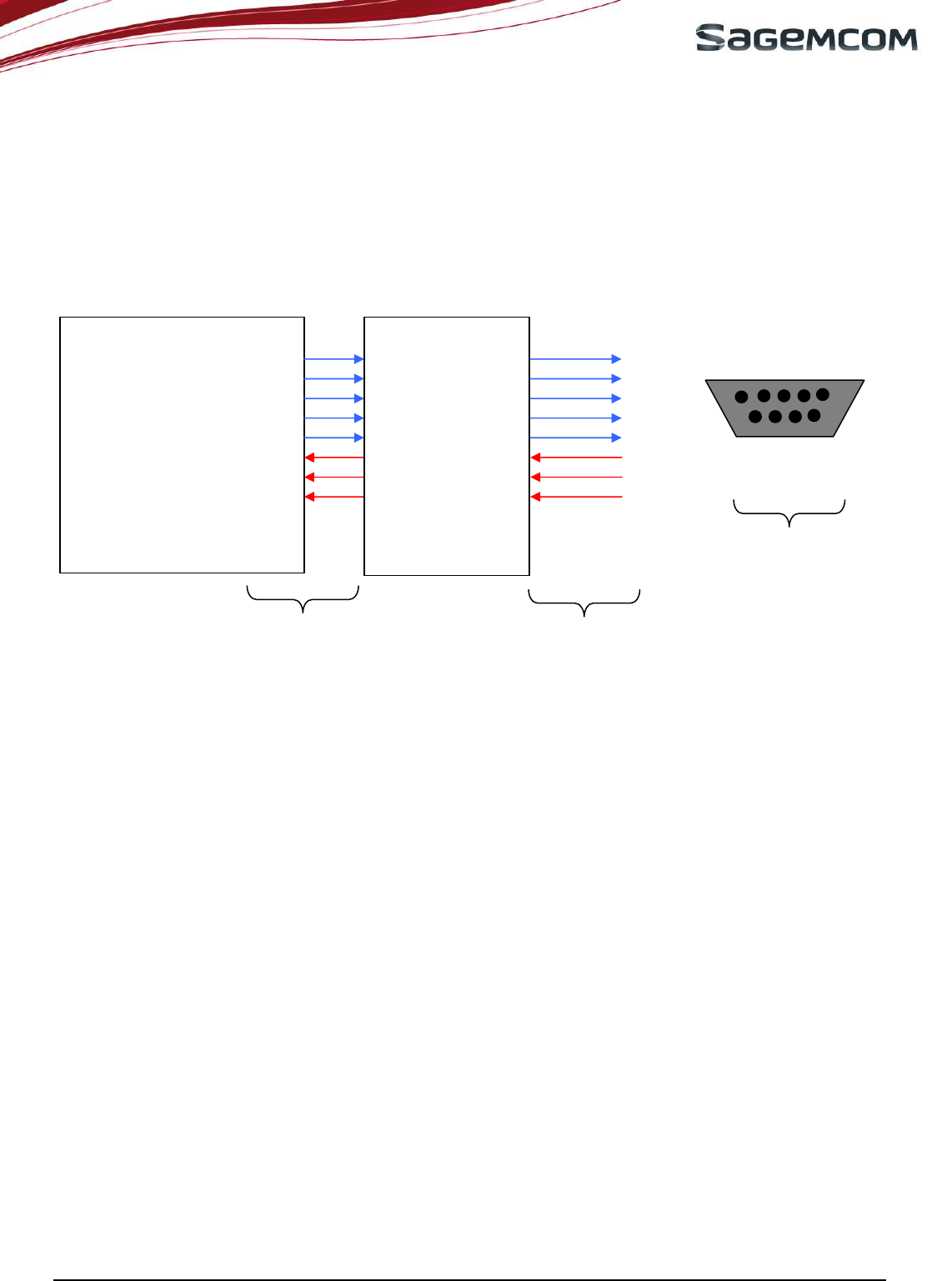
4.7.3 Complete V24 interface with PC
It supports speeds up to 115.2 Kbps and may be used in auto bauding mode.
To use the V24 interface, some adaptation components are necessary to convert the +2.8V signals from the
HiLoNC V2 to +/- 5V signals compatible with a PC.
Figure 20: connection to a data cable
Avoid supplying the UART before the HiLoNC V2 module is ON, this could result in bad power up
sequence. To have a proper behaviour use the signal VGPIO to enable the RS232 Transceiver.
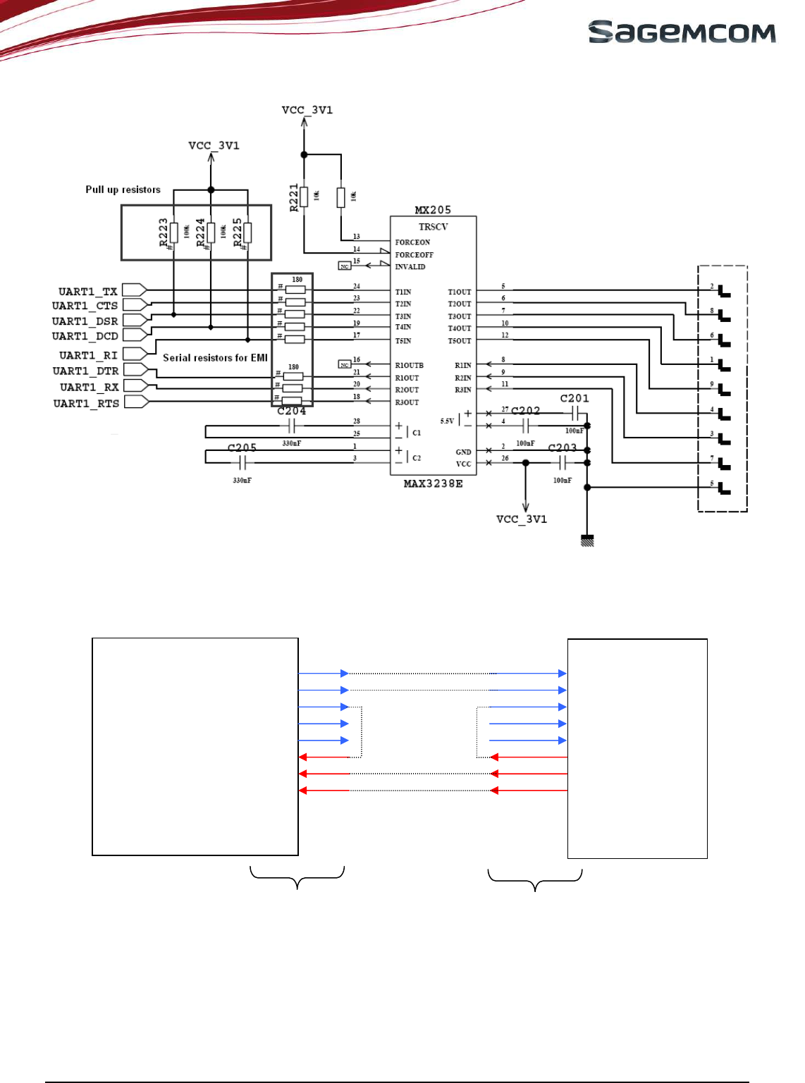
To create your own data cable (for software download purpose…etc…) refer to the following schematic as an
example with a MAX3238E:
• VCC_3V1 is an LDO output (VBAT to VCC_3V1) enabled by VGPIO from the module.
• 180Ω are serial resistors aimed to limit the EMC and ESD propagation.
RXD
CTS
DSR
DCD
RI
DTR
TXD
RTS
HiLoNC V2 Module
TXD
CTS
DSR
DCD
RI
DTR
RXD
RTS
RS232 Transceiver
IN
IN
IN
IN
IN
OUT
OUT
OUT
OUT
OUT
OUT
OUT
OUT
IN
IN
IN
DCE point of view DTE point of view
SUBD9 Female
Note: pin 5 is GND
1
6
9
5
2
8
6
1
9
4
3
7
2.8V signals 3.1V to +/-5.5V
signals
39
40
33
34
35
36
38
37
page 23/64
Note d’étude / Technical document : URD1– OTL
5665.3
– 003 / 72238 Edition 01
Document Sagemcom Reproduction et divulgation interdites
Sagemcom document. Reproduction and disclosure prohibited
Figure 21: Example of a connection to a data cable with a MAX3238E
4.7.4 Partial V24 (RX-TX-RTS-CTS) – connection HiLoNC V2 - host
When using only RX/TX/RTS/CTS instead of the complete V24 link, the following schematic could be used.
Figure 22: Partial V24 connection (4 wires) between HiLoNC V2 and host
As DSR is active (low electrical level) once the HiLoNC V2 is switched on, DTR is also active (low
electrical level), therefore AT command AT+Ksleep can switch between the two sleeps mode available for the
HiLoNC V2.
DTR input signal is internally pull upped to VGPIO with a 100KΩ, this result in 28µA of extra consumption.
RXD
CTS
DSR
DCD
RI
DTR
TXD
RTS
HiLoNC V2 Module
TXD
CTS
DSR
DCD
RI
DTR
RXD
RTS
DTE Device
2.8V signals
39
40
33
34
35
36
38
37
2.8V signals
Note: GND is not
represented
DCE point of view DTE point of view
page 24/64
Note d’étude / Technical document : URD1– OTL
5665.3
– 003 / 72238 Edition 01
Document Sagemcom Reproduction et divulgation interdites
Sagemcom document. Reproduction and disclosure prohibited
DCD and RI can stay not connected and floating when not used.
RI signal is a stand alone signal that can be used with anyone of the following configuration. Consult the
AT command specification for more information about this signal and its use.
This configuration allows to use the flow control RTS & CTS to avoid any overflow error during the data transfer,
CTS is moreover used to signal when the HiLoNC V2 is ready to receive an AT command after a power up
sequence or a wake up from sleep mode.
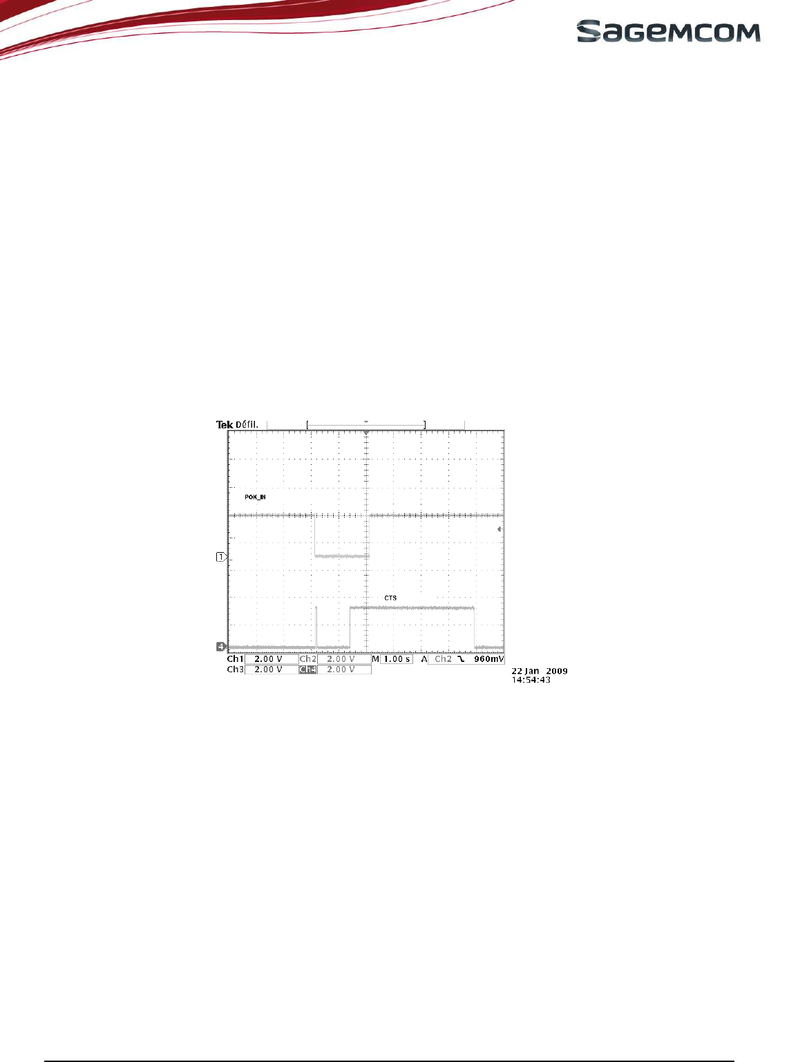
Figure 23: CTS versus POK_IN signal during the power on sequence.
However this configuration does not allow the signalling signals like:
• RI signal used when programmed to indicate an incoming voice or data call or SMS incoming etc…
• DCD signal used to signal the GPRS connections
• DSR signal used to signal the module UART interface is ON
• DTR signal used to prevent the HiLoNC V2 module from entering into sleep mode or to switch between
Data and AT commands or to hang up a call or to wake up the module etc…
Consult the AT command Specification document for the uses of the UART signals.
4.7.5 Partial V24 (RX-TX) – connection HiLoNC V2 - host
When using only RX/TX instead of the complete V24 link, the following schematic could be used.
Figure 24: Partial V24 connection (2 wires) between HiloNC V2 and host
DCE point of view DTE point of view
RXD
CTS
DSR
DCD
RI
DTR
TXD
RTS
HiLoNC V2 Module
TXD
CTS
DSR
DCD
RI
DTR
RXD
RTS
DTE Device
2.8V signals
39
40
33
34
35
36
38
37
2.8V signals
Note: GND is not
represented
page 25/64
Note d’étude / Technical document : URD1– OTL
5665.3
– 003 / 72238 Edition 01
Document Sagemcom Reproduction et divulgation interdites
Sagemcom document. Reproduction and disclosure prohibited
As DSR is active (low electrical level) once the HiLoNC V2 is switched on, DTR is also active (low
electrical level), therefore AT command AT+Ksleep can switch between the two sleep modes available for the
HiLoNC V2.
DTR input signal is internally pull upped to VGPIO with a 100KΩ, this result in 28µA of extra consumption.
As CTS is active (low electrical level) once the HiLoNC V2 is switched on, RTS is also active (low
electrical level), therefore AT command AT+Ksleep can switch between the two sleep modes available for the
HiLoNC V2. The HiLoNC V2's firmware allows the rise of CTS during the sleep state even when looped to RTS
signal.
DCD and RI can stay not connected and floating when not used.
RI signal is a stand alone signal that can be used with anyone of the following configuration. Consult the
AT command specification for more information about this signal and its use.
This configuration does not allow to use the flow control RTS & CTS. Those signals are used to avoid any
overflow error during the data transfer, CTS is moreover used to signal when the HiLoNC V2 is ready to receive
an AT command after a power up sequence or a wake up from sleep mode.
Figure 25: CTS versus POK_IN signal during the power on sequence.
Moreover this configuration does not allow the signalling signals like:
• RI signal used when programmed to indicate an incoming voice or data call or SMS incoming etc…
• DCD signal used to signal the GPRS connections
• DSR signal used to signal the module UART interface is ON
• DTR signal used to prevent the HiLoNC V2 module from entering into sleep mode or to switch between
Data and AT commands or to hang up a call or to wake up the module etc…
Consult the AT command Specification document for the uses of the UART signals.
4.8 UART0
HiLoNC V2 module manages a 2-wire UART interface. This UART interface is only dedicated for software
traces.
SAGEMCOM strongly recommends leaving this interface externally accessible for trace (e.g. access by
test point pads).
page 26/64
Note d’étude / Technical document : URD1– OTL
5665.3
– 003 / 72238 Edition 01
Document Sagemcom Reproduction et divulgation interdites
Sagemcom document. Reproduction and disclosure prohibited
4.9 GPIO
There are Three GPIOs available on HiloNC V2. All GPIOs have internal pull-up resistors.
GPIOs can directly be controlled with dedicated AT commands.
Thanks to some other special AT commands, GPIOs can for example be used:
• to make an I/O toggling while the module is attached to the network
• to make an I/O toggling when a programmed temperature is reached
• as input to detect the presence of an antenna (with some external additional electronic)
• as input to detect the SIM card presence …etc
4.10 ADC
There is one ADC input pad which can be used to read the value of the voltage applied. Following
characteristics must be met to allow proper performances:
• The input signal voltage must be within 0V and up to 3V
• The input impedance of the pad is 150KΩ
• The input capacitance is typically 10pF.
The AT command AT+KADC will give voltage value with following characteristics:
• 10 bits resolution
• Maximum sampling frequency is 200 KHz.
Consult the AT command Specification document for more information about KADC AT command.
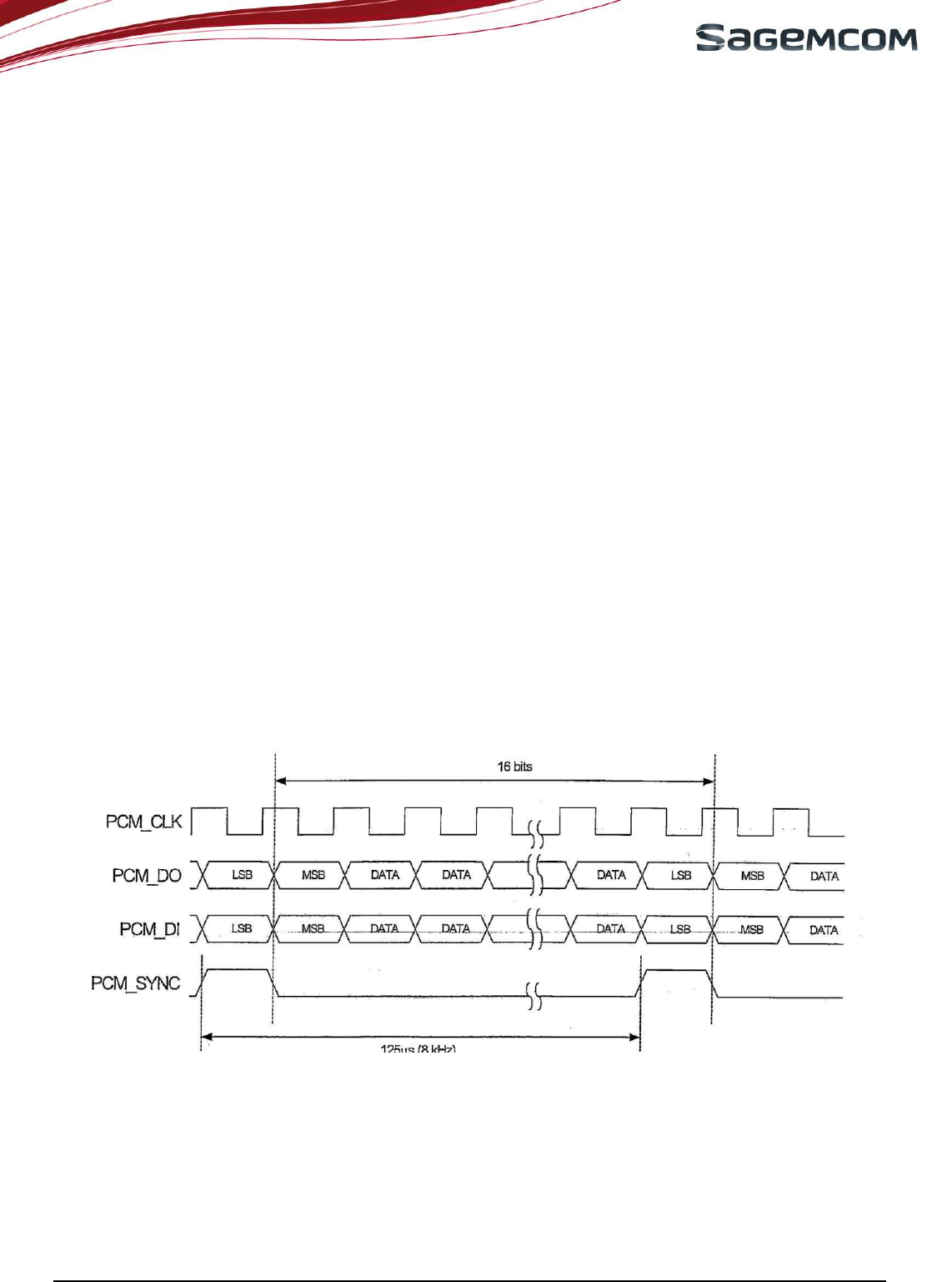
4.11 PCM
There is a master PCM interface available on HiLoNC V2. The PCM interface can be configured by dedicate AT
commands. Following characteristics must be met:
• 16 bits PCM data word length
• Configurable PCM clock rate must not exceed 1MHz
Figure 26: PCM interface timing
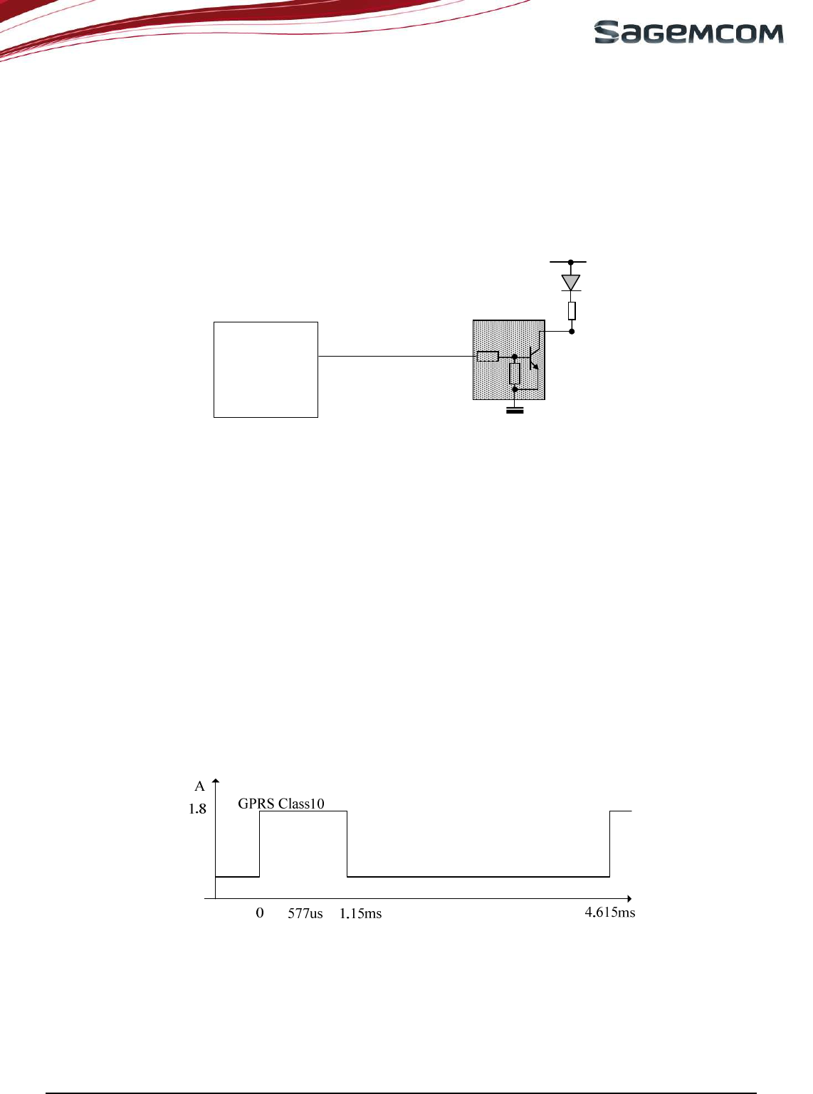
4.12 RF BURST INDICATOR
There is one digital output named RF_TX available on HiLoNC V2 to indicate the RF transmission. This output
can not be controlled by AT commands and can not be used for other purpose.
This output can only connect to a transistor but not to drive a LED directly. Otherwise, the RF
transmission will be unexpected affected.

page 27/64
Note d’étude / Technical document : URD1– OTL
5665.3
– 003 / 72238 Edition 01
Document Sagemcom Reproduction et divulgation interdites
Sagemcom document. Reproduction and disclosure prohibited
Figure 27: RF_TX burst indicator
4.13 BACKUP BATTERY
4.13.1 Backup battery function feature
4.13.1.1 With backup battery
A backup battery can be connected to the module in order to supply internal RTC (Real Time Clock) when the
main power supply is removed. Thus, when the main power supply is removed, the RTC is still supplied and the
module keeps the time register running.
With external backup battery:
• If VBAT < 3V, internal RTC is supplied by VBACKUP.
• If VBAT ≥3V, internal RTC is supplied by VBAT.
4.13.1.2 Without backup battery
Without backup battery
• If VBAT ≥ 1.5V, internal RTC is supplied by VBAT.
• If VBAT < 1.5V, internal RTC is not supplied.
VBACKUP input of the module has to be connected to a 10µF capacitor (between VBACKUP and GND).
SAGEMCOM does not recommend to connecting VBACKUP signal to VBAT as for former SAGEMCOM
MOXX modules.
4.13.2 Current consumption on the backup battery
When the power supply is removed, the internal RTC will be supplied by backup battery.
To calculate the backup battery capacity, consider that current consumption for RTC on the backup
battery is up to 1000µA depending on the temperature.
RF_TX
HiLoNC
V2
VBAT
R
page 28/64
Note d’étude / Technical document : URD1– OTL
5665.3
– 003 / 72238 Edition 01
Document Sagemcom Reproduction et divulgation interdites
Sagemcom document. Reproduction and disclosure prohibited
Pad Name
Min Max
VBACKUP
1000µA
4.13.3 Charge by internal HiLoNC V2 charging function
The charging function is available on the HiLoNC V2 without any additional external power supply (the charging
power supply is provided by the HiLoNC V2).
Charge of the back-up battery occurs only when main power supply VBAT is provided.
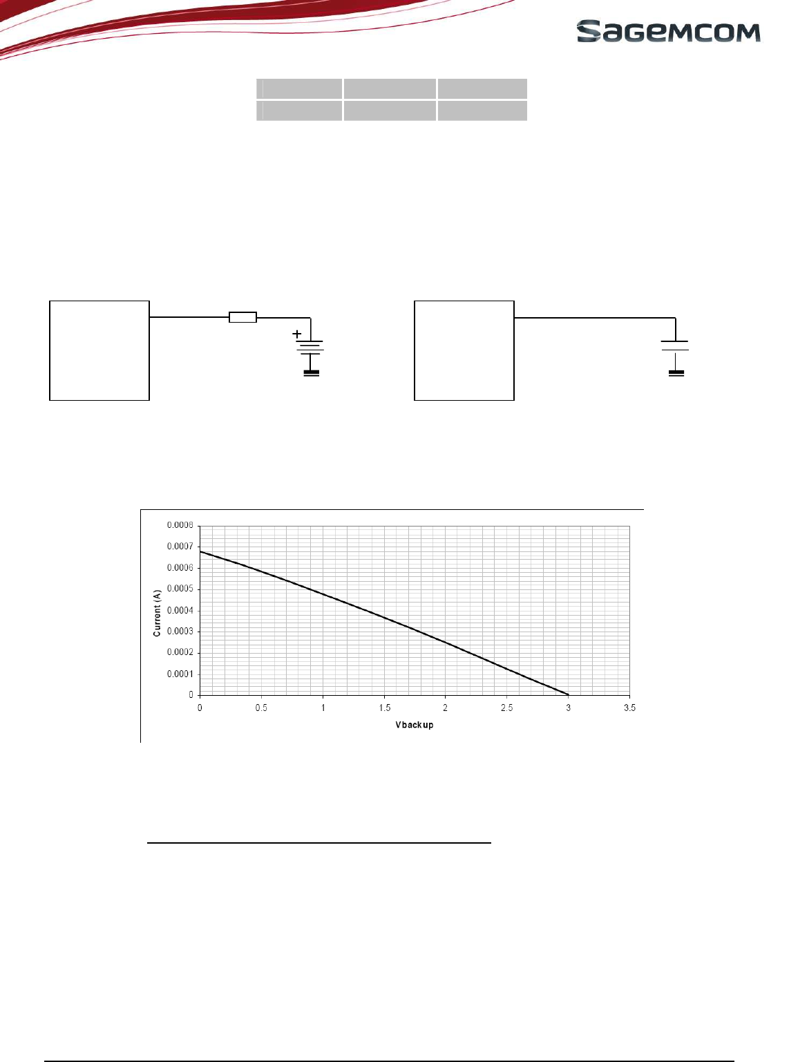
The recommended schematic is given hereafter:
Figure 28: Backup battery or 10µF Capacitor internally charged
The resistor R depends on the charging current value provided by the battery manufacturer.
The charging curve which is done by the HiLoNC V2 is given hereafter:
Figure 29: Charging curve of backup battery
4.13.4 Backup Battery technology
4.13.4.1 Manganese Silicon Lithium-Ion rechargeable Battery
SAGEMCOM does not recommend using this kind of technology because of the following drawbacks:
• The maximum discharge current is limited (Shall be compliant with the module characteristics).
• The over-discharge problem: most of the Lithium Ion rechargeable batteries are not able to recover their
charge when their voltage reaches a low-level voltage. To avoid this, it is necessary to add a safety
component to disconnect the backup .battery in case of over–discharge condition. In such a case, this
implementation is too complicated (too much components for that function).
• The charging current has to be regulated.
SAGEMCOM does not recommend using this kind of backup battery technology.
VBACKUP
HiLoNC V2
10µF capacitor
VBACKUP
HiLoNC V2
R
Backup battery

page 29/64
Note d’étude / Technical document : URD1– OTL
5665.3
– 003 / 72238 Edition 01
Document Sagemcom Reproduction et divulgation interdites
Sagemcom document. Reproduction and disclosure prohibited
4.13.4.2 Capacitor battery
These kinds of backup battery have not the drawbacks of the Lithium Ion rechargeable battery.
As there are only capacitors:
• The maximum discharge current is generally bigger,
• There is no problem of over-discharge: the capacitor is able to recover its full charge even if its voltage
has previously fallen to 0V.
• There is no need to regulate the charging current.
Moreover, this kind of battery is available in the same kind of package than the Lithium Ion cell and fully
compatible on a mechanical point of view. The only disadvantage is that the capacity of this kind of battery is
significantly smaller than Manganese Silicon Lithium Ion battery. But for this kind of use (supply internal RTC
when the main battery is removed), the capacity is generally enough.
SAGEMCOM strongly recommends using this kind of backup battery technology.

page 30/64
Note d’étude / Technical document : URD1– OTL
5665.3
– 003 / 72238 Edition 01
Document Sagemcom Reproduction et divulgation interdites
Sagemcom document. Reproduction and disclosure prohibited
4.14 START THE MODULE PROPERLY AND AVOID POWER UP ISSUES.
This chapter gives advices on how to make a proper start of the HiLoNC V2 module and sums up the side
effects of a non compliant power up sequence or a non compliant hardware connection between the HiLoNC V2
and the host CPU.
4.14.1 Power domains
Each HiLoNC V2 pad is linked to a specific internal power domain as the following:
• VANA is typically 2.85V and is a general purpose analogue dedicated voltage.
• VBAT is typically 3.2V to 4.5V and is the main system voltage.
• VRTC is typically 3.0V and is the real time clock dedicated voltage.
• VGPIO is typically 2.8V and is a general purpose digital dedicated voltage.
• VSIM is typically 1.8V or 2.9V and is the digital SIM card function dedicated voltage.
• VPERM is typically 3.0V and is the permanent voltage dedicated to launch the power up sequence.
The next table gives the 51 HiLoNC V2 pads with all their relative power domains.
HiLoNC
Pads Signal Name Function Power domain
E1 /INTMIC_P AUDIO 2.85V
E2 /AUX_ADC0 ADC 2.85V
E3 GND POWER 0V
E4 VGPIO EXT_VDD 2.8V
E5 VBACKUP EXT_VDD 3.0V
E6 /PWM0 PWM 2.85V
E7 /RESET_IN RESET 2.8V
E8 SAGEMCOM FACTORY USE 2.8V
E9 SAGEMCOM FACTORY USE 2.8V
E10 SAGEMCOM FACTORY USE 2.8V
E11 SAGEMCOM FACTORY USE 2.8V
E12 SAGEMCOM FACTORY USE 2.8V
E13 NTRST JTAG/FACTORY
2.8V
E14 /GPIO2 GPIO 2.8V
E15 /GPIO1 GPIO 2.8V
E16 /RF_TX RF 2.8V
E17 /PCM_CLK PCM 2.85V
E18 /PCM_SYNC PCM 2.85V
E19 /PCM_OUT PCM 2.85V
E20 /PCM_IN PCM 2.85V
E21 GND POWER 0V
E22 / JTAG1 JTAG 2.8V
E23 /JTAG2 JTAG 2.8V
E24 /TEST JTAG 2.8V
E25 /UART0_RXD UART 0 2.85V
Figure 30 : HiLoNC V2 51 pads with their power domains
page 31/64
Note d’étude / Technical document : URD1– OTL
5665.3
– 003 / 72238 Edition 01
Document Sagemcom Reproduction et divulgation interdites
Sagemcom document. Reproduction and disclosure prohibited
HiLoNC
Pads Signal Name Function Power domain
E26 /GPIO3 GPIO 2.8V
E27 GND RF 0V
E28 /ANTENNA RF 3.7V
E29 GND RF 0V
E30 VBATT POWER 3.7V
E31 VBATT POWER 3.7V
E32 /UART0_TXD UART 0 2.85V
E33 /UART1_DSR UART 1 2.8V
E34 /UART1_DCD UART 1 2.8V
E35 /UART1_RI UART 1 2.8V
E36 /UART1_DTR UART 1 2.8V
E37 /UART1_RTS UART 1 2.85V
E38 /UART1_RX UART 1 2.85V
E39 /UART1_TX UART 1 2.85V
E40 /UART1_CTS UART 1 2.85V
E41 /POK_IN POWER ON 3.0V
E42 /PWM2 PWM 2.85V
E43 /PWM1 PWM 2.85V
E44 /SIM_CLK SIM 1.8V or 2.9V
E45 /SIM_RST SIM 1.8V or 2.9V
E46 /SIM_DATA SIM 1.8V or 2.9V
E47 VSIM SIM 1.8V or 2.9V
E48 VBATT POWER 3.7V
E49 GND POWER 0V
E50 /HSET_OUT_P AUDIO 3.7V
E51 /HSET_OUT_N AUDIO 3.7V
Figure 31 : HiLoNC V2 51 pads with their power domains…continued
4.14.2 IO DC PRESENCE BEFORE POWER ON.
When the VBAT is available but the module not yet started, the following I/O's raised their output.
• VBACKUP raise to 3V
• POK_IN raise to 3V
• HSET_N raise to 1.4V
• HSET_P raise to 1.4V
4.14.3 SIDE EFFECTS OF A RETRO SUPPLY (CURRENT RE-INJECTION)
Interactions or connections between the HiLoNC V2 module and the external systems can lead to retro power
supply side effects, or current re-injection through pads while the module is not yet fully powered up (means
VBAT lower than its minimum 3.2V).
If some precaution and simple rules are not followed, those effects can in worst case result in a deadlock
module, not able to start up or to communicate.
Deadlock could happen if the retro supply occurs before the module start. The flow back current could in the
worst case prevent the module to start.
The very same behaviour can happen in a normal use conditions when the lines connecting to the module to the
external system uses a non compliant voltage higher than the module IO power domain (2.85V). This results in
a current flow back inside the module and can lead to a deadlock system on the next start if this retro supply
has continued while the system was powered off or under powered (under 3.2V).
An over voltage on any line can also damage the HiLoNC V2 module.
Those consequences are very rare but exist. Therefore, the rules and advises given on every chapter of this
application note must be followed.
page 32/64
Note d’étude / Technical document : URD1– OTL
5665.3
– 003 / 72238 Edition 01
Document Sagemcom Reproduction et divulgation interdites
Sagemcom document. Reproduction and disclosure prohibited
To avoid any power up issue, here are the rules:
Avoid any over voltage on the buses lines connected to the module.
When the module is off, do not apply any voltage on lines connected to the module.
The over voltage can be avoided by using the same power domain voltage.
Avoid 5V or 3.3V systems straight connection to 2.8V HiLoNC V2 lines.
Use level adaptors when the power domain requires it.
When the module is off:
Powers off the buses lines of the main system that are connected to the module, this avoid any flow back
current (re-injection) and of course help a lot to improve and control the power consumption. This last issue is
important as in off mode there is not control of the current inside the module and can results in a loss of current
by leakage through the I/Os of the module.
4.14.4 EXAMPLE OF A CURRENT RE-INJECTION ON U.A.R.T.
Current re-injection appears when the module is off or not powered and I/Os connected to the module still
powered. Example: UART bus powered from the DTE side before the module is powered. This can result in a
bad starting behaviour.
To avoid current re-injection, simply do not supply the lines connected to the module before the module
switches on. Power up the module first using the POK_IN Line then open the UART lines for the DTE side and
all necessary I/O, this will avoid leakage of current improving the power consumption and avoid any possible
deadlock issue during the power up process.
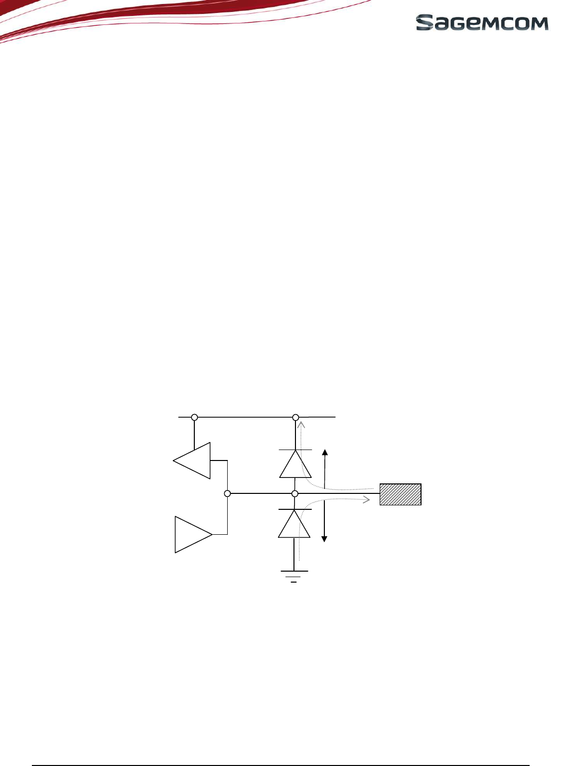
Figure 32: Digital Pad-out clamp diode
All the digital pads have this structure a current re-injection by supplying the lines with a non compliant
voltage range must be avoided. (From -0.4V up to 2.8V+0.4V)
Reverse currents over 15mA will damage the chip. Avoid this issue. Keep the connected line voltage
between 0 and 2.8V.
For an interface with a CMOS 3.3V system or TTL 5V system, use level adapters powered by 2 supplies:
a 2.8V from a LDO IC which is enabled by VGPIO signal and the other external required voltage 3.3V or 5V.
If a Level shifter is used or a RS232 adapter, use the VGPIO signal as the enable signal to avoid any
current re-injection before the module start.
Power supply domain
Pad_X
IN Buffer
OUT Buffer
Vd = 0.4V
Vd = 0.4V
I max = 15mA
I max = 15mA
Clamp
Diode
Clamp
Diode
page 33/64
Note d’étude / Technical document : URD1– OTL
5665.3
– 003 / 72238 Edition 01
Document Sagemcom Reproduction et divulgation interdites
Sagemcom document. Reproduction and disclosure prohibited
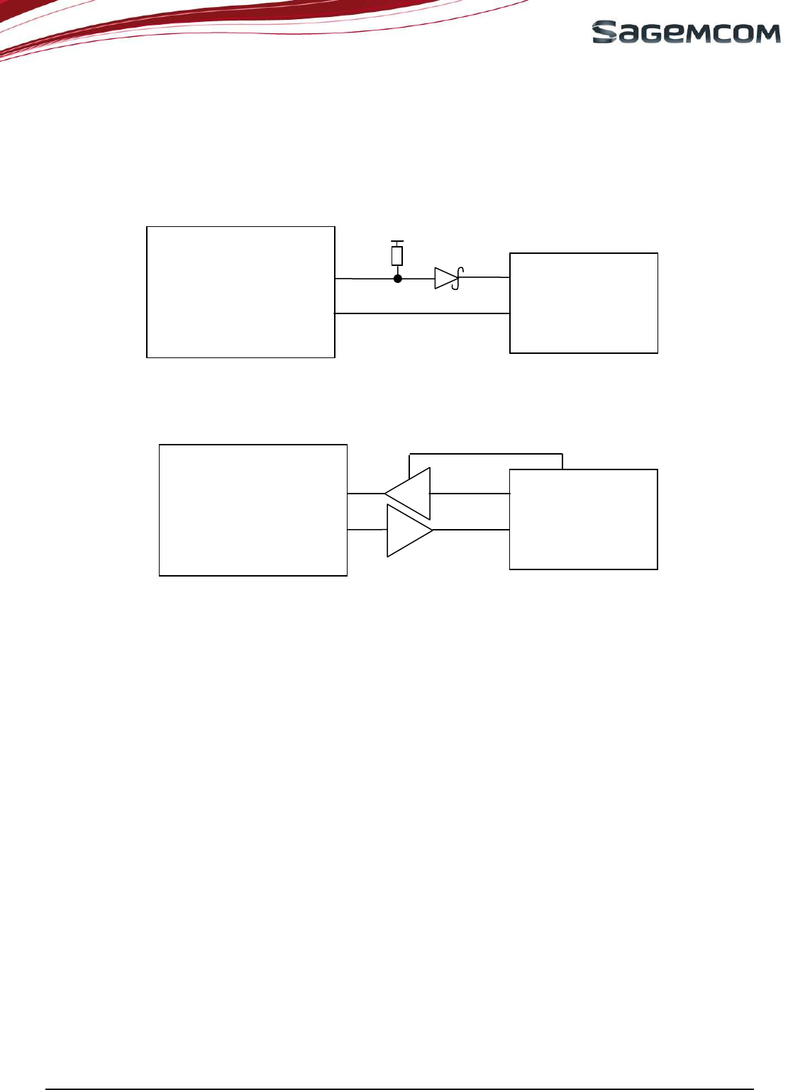
If a straight connection is used between the HiLoNC V2 and the DTE UART it is necessary to isolate host
and HiLoNC V2 module in order to avoid generating current re-injection through when HiLoNC V2 is switched-
off.
Example of schematic (only useful signals are represented):
Figure 33: Hardware interface diodes solution between HiLoNC V2 and host
Figure 34: Hardware interface buffers solution between HiLoNC V2 and host
4.14.5 ADVICES FOR EVERY POWER DOMAIN
• To avoid any current re-injection on VANA (2.85V)
If an external bias voltage over VANA is used for the microphone, use a 10µF serial capacitor to block the
DC voltage.
If a voltage higher than VANA has to be measured by the ADC, use external resistor divider to limit it.
if PWM bus is output only, the external system is supposed to be in input on the same voltage domain, if it is
not the case or if its inputs are pulled up and able to source current while the module is off, then simply use
open drain or open collector transistors to avoid any flow back current to the module.
The external system connected to the module by the UART has to switch its UART lines off while the module
is off. If the external system cannot commands its UART lines off, then it is necessary to add a buffer between
the module and the external system to prevent any issue. In this last case, the buffer would have to be enabled
by the VGPIO voltage that is only available when the module starts. This applies to TXD, RXD, RTS, CTS which
are on this power domain and also to the lines on the VGPIO power domain (see here after).
• To avoid any current re-injection on VGPIO (2.80V)
Do not connect a power supply to the VGPIO pad. This pad is an LDO output only.
The reset signal is internally pulled up and can be connected to an open drain transistor.
The GPIOs have to be used in compliance of the power domain and when the module is off, the external
system has to shut off its GPIOs.
The SPI bus has to be not connected to the external system.
The JTAG bus has to be not connected to the external system.
The UART lines on this power domain (DCD, DTR, DSR, RI) have to follow the same rules as those on
VANA domain (TXD, RXD, RTS, CTS). See have above.
A resistor of 10KΩ has to be connected to the E11 (NTRST) pad and GND to pull down this I/0, preventing
any deadlock due to VGPIO current re-injection.
Tri state command
Buffer
Host
HiLoNC V2
DTR, RTS, RXD
DCD, DSR, CTS, TXD, RI
DTR, RTS, RXD
DCD, DSR, CTS, TXD, RI
HiLoNC V2
Host
VGPIO

page 34/64
Note d’étude / Technical document : URD1– OTL
5665.3
– 003 / 72238 Edition 01
Document Sagemcom Reproduction et divulgation interdites
Sagemcom document. Reproduction and disclosure prohibited
• To avoid any current re-injection on VPERM (3.0V)
The POK_IN signal is internally pulled up and can be connected to an open drain transistor.
• To avoid any current re-injection on VRTC (3.0V)
The VBACKUP signal has to be only connected to a DC coin 3V battery or a capacitor of 10µF.
• To avoid any current re-injection on VSIM (1.8V or 2.9V)
Use only VSIM pads to supply the sim card or sim chip.
• To avoid any current re-injection on VBAT (3.2V to 4.5V)
Use a VBAT signal with a fast rise time to have a VBAT final value as fast as possible. (see hereafter)
In case of needs, use 2 serial capacitors of 10µF to connect the audio speaker lines to the external system
inputs.
4.14.6 CASE OF VBAT RISE TIME
The VBAT rise time from 0V to its final value has to be lower than 1ms
(1)
. This is necessary in order to avoid any
possible failure during the power up. If this value cannot be guaranteed, then some MOS transistors could be
used to create a fast rise time switch able to quickly commute from the VBAT final value to the modules power
pads.
(1)
This value will be updated to a higher final value including the worst case.
4.14.7 START- UP
To start the module, first power up VBAT, which must be in the range 3.2V ~ 4.5V, and able to provide 2.2A
during the TX bursts
(Refer to the module specification for more details).
POK_IN is a low level active signal internally pulled up to a dedicated power domain to 3V.
As POK_IN is internally pulled up, a simple open collector or open drain transistor can be used for ignition.
To start the module, a low level pulse must be applied on POK_IN during 2000 ms.
RESET must not be Low during that period of time
After a few seconds, the CTS goes to the active state when the module is ready to receive AT commands.
VGPIO is a supply output from the module that can be used to check if the module is alive.
• When VGPIO = 0V the module is OFF
• When VGPIO = 2.8V the module is ON (It can be in Idle, communication or sleep modes)
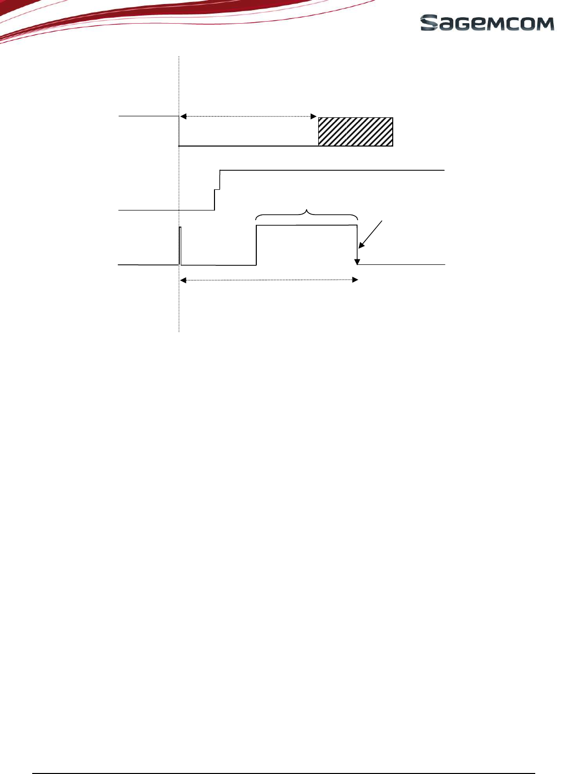
page 35/64
Note d’étude / Technical document : URD1– OTL
5665.3
– 003 / 72238 Edition 01
Document Sagemcom Reproduction et divulgation interdites
Sagemcom document. Reproduction and disclosure prohibited
Figure 35: Power ON sequence
POK_IN
VGPIO
spike
Software Loading
Module is ready
to receive AT
commands
Module is
OFF
Module is
ON
2000ms
CTS
Typ 5 seconds
Max 7 seconds
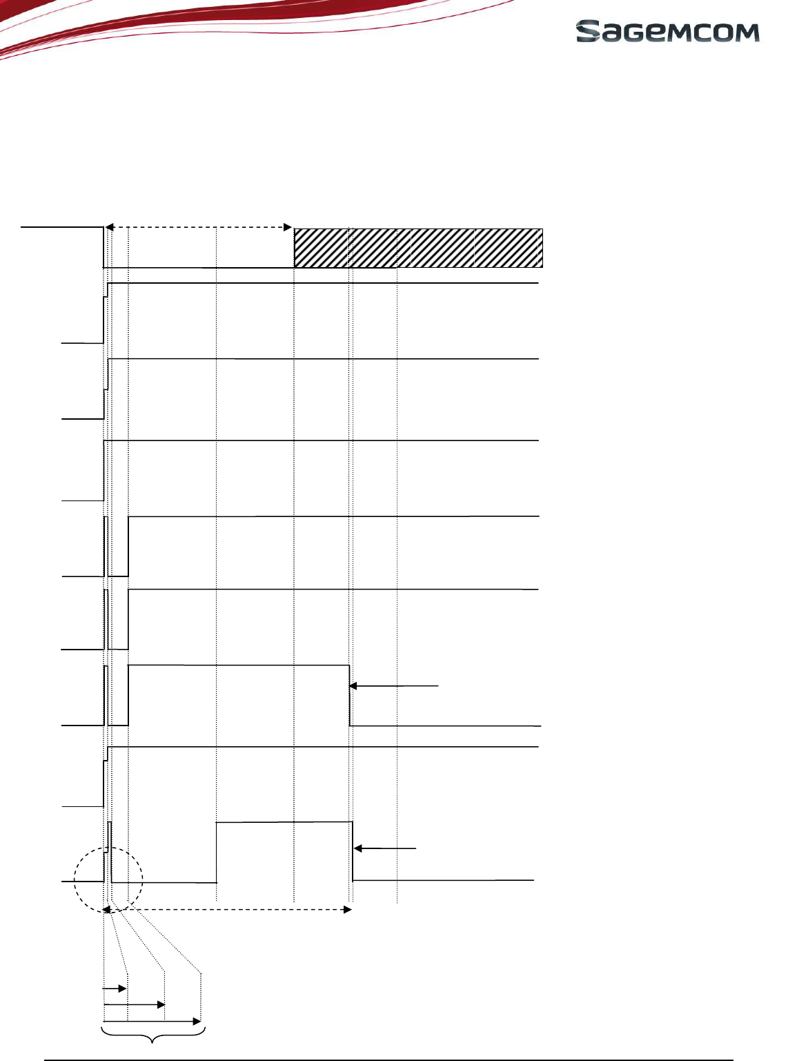
page 36/64
Note d’étude / Technical document : URD1– OTL
5665.3
– 003 / 72238 Edition 01
Document Sagemcom Reproduction et divulgation interdites
Sagemcom document. Reproduction and disclosure prohibited
4.15 UART SIGNALS AT POWER ON
The UART signals are low level active therefore these signals rise up when the module starts. During around
70ms (see figure below), those signals present a transient spike. Those spikes behaviour at start up are normal,
however pay attention to them when a CTS low level detection is used do send AT commands. Only DSR and
CTS signals get low after the end of the start up procedure.
Figure 36: Full UART signals during the power on sequence.
Module is ready to
receive AT commands
TXD
RXD
DTR
RI
DCD
DSR
RTS
Module UART
interface is ON
Typ 5 seconds
Max 7 seconds
70ms
30ms
150ms
Transients spikes
during power on
sequence
Module is
OFF
Module is ON
POK_IN
2000ms
CTS
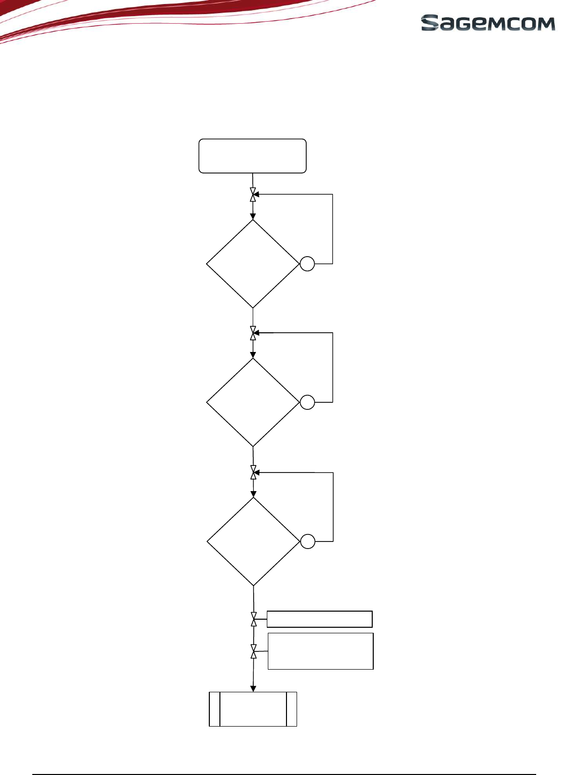
page 37/64
Note d’étude / Technical document : URD1– OTL
5665.3
– 003 / 72238 Edition 01
Document Sagemcom Reproduction et divulgation interdites
Sagemcom document. Reproduction and disclosure prohibited
4.16 POWER ON AND SLEEP DIAGRAMS
Those 2 diagrams show the behaviours of the module and the DTE during the power on and then in the sleep
modes.
Figure 37: Diagram for the power on
DTE is in idle mode
VGPIO rise to 2.8V
U.A.R.T.
closed ?
VBAT≥3.2
Volts min
stable?
POK_IN
LOW for 2s
AND Reset
High?
CTS is Low and /or
KSUP
notified if KSREP
activated
Module is ready
to receive and
send AT
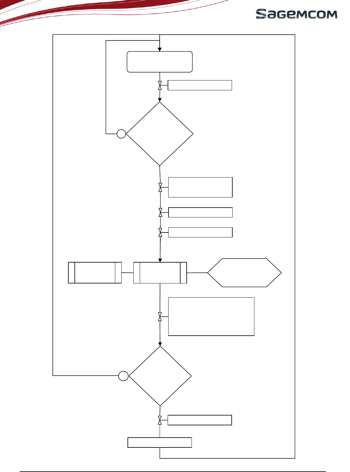
page 38/64
Note d’étude / Technical document : URD1– OTL
5665.3
– 003 / 72238 Edition 01
Document Sagemcom Reproduction et divulgation interdites
Sagemcom document. Reproduction and disclosure prohibited
Figure 38: Diagram for the sleep mode
Ksleep = 1 OR
( Ksleep = 0
AND
DTR = High)
Module is ready to
receive and send AT
VGPIO remains at 2.8V
RI signal
connected
and
programmed?
Module is in
sleep mode
Sleep mode request
Delay to enter the sleep
mode
CTS is High
The wakes up
periods are set by
the network DRX
or the OS
DTE could
also
be in sleep
mode
Wake up incoming event such as:
• Network event.
• Alarm interruption.
• DTR interruption.
• RTS interruption.
RI wakes the DTE
DTE is in idle mode
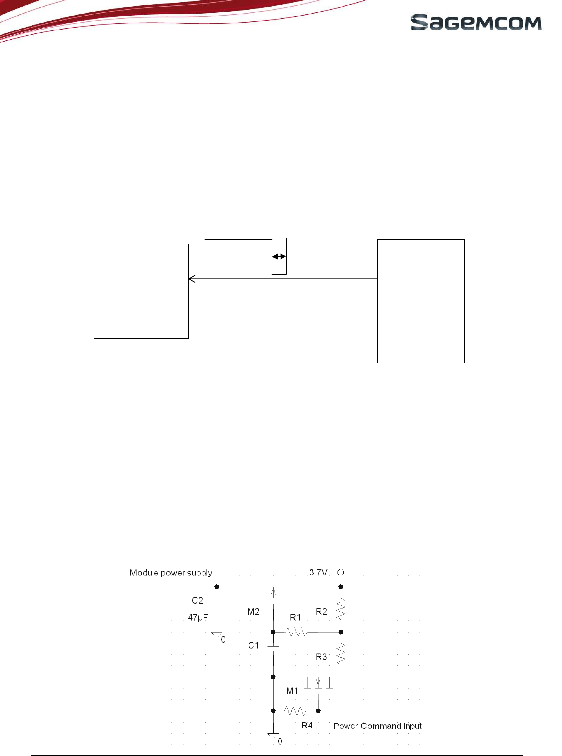
page 39/64
Note d’étude / Technical document : URD1– OTL
5665.3
– 003 / 72238 Edition 01
Document Sagemcom Reproduction et divulgation interdites
Sagemcom document. Reproduction and disclosure prohibited
4.17 MODULE RESET
To reset the module, a low level pulse must be sent on RESET pad during 10 ms. This action will immediately
restart the HiLoNC V2 module. It is therefore useless to perform a new ignition sequence (POK_IN) after.
SAGEMCOM recommends using this feature in case of emergency, freeze of module or abnormal longer
time to respond to AT Commands, this signal is the only way to get the control back over the HiLoNC V2
module.
RESET is a low level active signal internally pulled up to a dedicated power domain.
As RESET is internally pulled up, a simple open collector or open drain transistor can be used to control it.
Figure 39: Reset command of the HiLoNC V2 by an external GPIO
The RESET signal will reset the registers of the CPU and reset the RAM memory as well.
As RESET is referenced to VGPIO domain (internally to the module) it is impossible to make a reset
before the module starts or try to use the RESET as a way to start the module.
An other solution more costly would be to use MOS transistor to switch off the power supply and restart the
power up procedure using the POK_IN input line.
4.18 MODULE SWITCH OFF
An AT command “AT*PSCPOF” allows to switch off «properly" the HiLoNC V2 module.
In case of necessary the module can be switched off by controlling the power supply. This can be used for
example when the system freezes and no reset line is connected to the HiLoNC V2. In this case the only way to
get the control back over the module is to switch off the power line. If the system is on a battery, it is wise to
have a control of the power supply by a GPIO with for example the following schematic.
SAGEM HiLoNC
V2 Module
DCE
HOST DTE
RESET_IN: 7
10ms
2.4V min
0.4V max
GPIO
2.8V
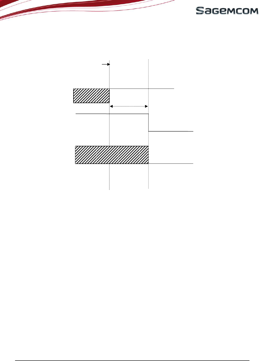
page 40/64
Note d’étude / Technical document : URD1– OTL
5665.3
– 003 / 72238 Edition 01
Document Sagemcom Reproduction et divulgation interdites
Sagemcom document. Reproduction and disclosure prohibited
Figure 40: Power supply command by a GPIO
This kind of schematic could also be used to save few micro amperes in case of need. As the module has
a drain current of up to 56µA, this kind of function could lower it to the current through R4.
These, are the behaviours of the VGPIO and the CTS signal during the power off sequence.
Figure 41: Power OFF sequence for POK_IN, VGPIO and CTS
4.19 SLEEP MODE MANAGEMENT AND POWER CONSUMPTION
The AT command “AT+KSLEEP” allows to configure the sleep mode.
When AT+KSLEEP=1 is configured:
• The HiLoNC V2 module decides by itself when it enters in sleep mode (no more task running).
• “0x00” character on serial link wakes up the HiLoNC V2 module.
When AT+KSLEEP=0 is configured:
• The HiLoNC V2 module is active when DTR signal is active (low electrical level).
• When DTR is deactivated (high electrical level), the HiLoNC V2 module enters in sleep mode after a
while.
• On DTR activation (low electrical level), the HiLoNC V2 module wakes up.
When AT+KSLEEP=2 is configured:
• The HiLoNC V2 module never enters in sleep mode.
In sleep mode the module reduces its power consumption and remains waiting for the wake up signals either
from the network (i.e. Read paging block depending on the DRX value of the network) or the operating system
(i.e. timers wake up timers activated) or the host controller (i.e. character on serial link or DTR signal).The
power consumption should look like the following example for DRX9.
POK_IN Internal
pull up to 3V
*Must be High
VGPIO
Module is ON Module is
OFF
Typ 2 seconds
AT*PSCPOF
CTS
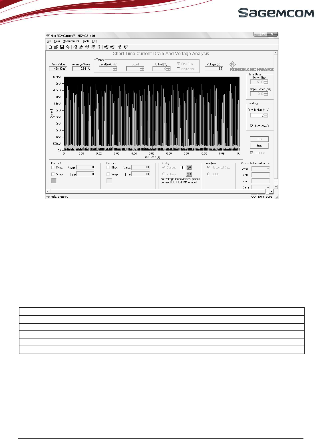
page 41/64
Note d’étude / Technical document : URD1– OTL
5665.3
– 003 / 72238 Edition 01
Document Sagemcom Reproduction et divulgation interdites
Sagemcom document. Reproduction and disclosure prohibited
Figure 42: Power consumption at DRX9 (with RS-NGMO2 power supply)
When the HiLoNC V2 module leaves the sleep mode thanks to the network incoming signal or by action of the
user the power consumption will step from the <1.7mA to 15mA and then to 25mA in around 2 seconds.
The behaviour of the system at wake-up:
• System resumes from clock 32 MHz, the power consumption rises to around 15mA.
• System resumes the hardware blocks, the power consumption rises to around 25mA.
To perform the correct measurement of the power supply of a system using a HiLoNC V2 module, refer to
the specification TW0.9 version 4.7 June 2008 chapter "standby test procedure" from the GSM
association. This specification explains how to proceed and what apparatus have to be used to perform
the test.
Check also SAGEMCOM document "Getting started with the current consumption measurement"
The main parameters for a compliant measurement are:
Parameter Idle Mode Setting Idle Mode Setting
Measurement Serial Resistance 0.5 ohms
Tolerance/Type.
1%, 0.5W, high precision metal film resistor
Sampling frequency 50 k samples/s
Resolution 0.1mA over the full dynamic range of module currents
Noise floor Less than lowest ADC step

page 42/64
Note d’étude / Technical document : URD1– OTL
5665.3
– 003 / 72238 Edition 01
Document Sagemcom Reproduction et divulgation interdites
Sagemcom document. Reproduction and disclosure prohibited
5. RECOMMENDED I/OS AND COMPONENTS ON THE FINAL PRODUCT
The design of the customer’s board (on which the module is soldered) must
provide an access to following
signals when the final product will be completely
integrated.
To upgrade the module software, SAGEMCOM recommends providing a direct access to the module
serial link through an external connector or any mechanism allowing the upgrade of the module without
opening the whole product.
Serial link:
TXD Output UART transmit
RXD Input UART receive
To trace the module software, SAGEMCOM recommends providing a direct access to the module trace
port UART0 (2 I/Os) through internal test points (TP) located on the customer's main board.
The board has to feature as minimum those external components.
A capacitor of 47µF on the VBAT near pads 30 and 31.
A capacitor of 10µF on VBACKUP when no backup battery is used.
6. ESD & EMC RECOMMENDATIONS
6.1 HILONC V2 ALONE
The HiLoNC V2 module alone can hold up to 2KV on each of the 51 pads including the RF pad.
6.2 HANDLING THE MODULE
HiLoNC V2 modules are designed and packaged in tape-and-real for factories SMT process.
HiLoNC V2 modules contain electronic circuits sensitive to human hand's electrostatic electricity.
Handling without ESD protection could result in permanent damages or even destruction of the module.
6.3 Customer’s product with HiLONC V2
If customer’s design must stand more than 2kV on electrostatic discharge, following recommendation must be
followed.
6.4 Analysis
ESD current can penetrate inside the device via the typical following components:
• SIM connector
• Microphone
• Speaker
• Battery / data connector
• All pieces with conductive paint.
In order to avoid ESD issues, efforts shall be done to decrease the level of ESD current on electronic
components located inside the device (customer’s board, input of the HiLoNC V2 module, etc…)
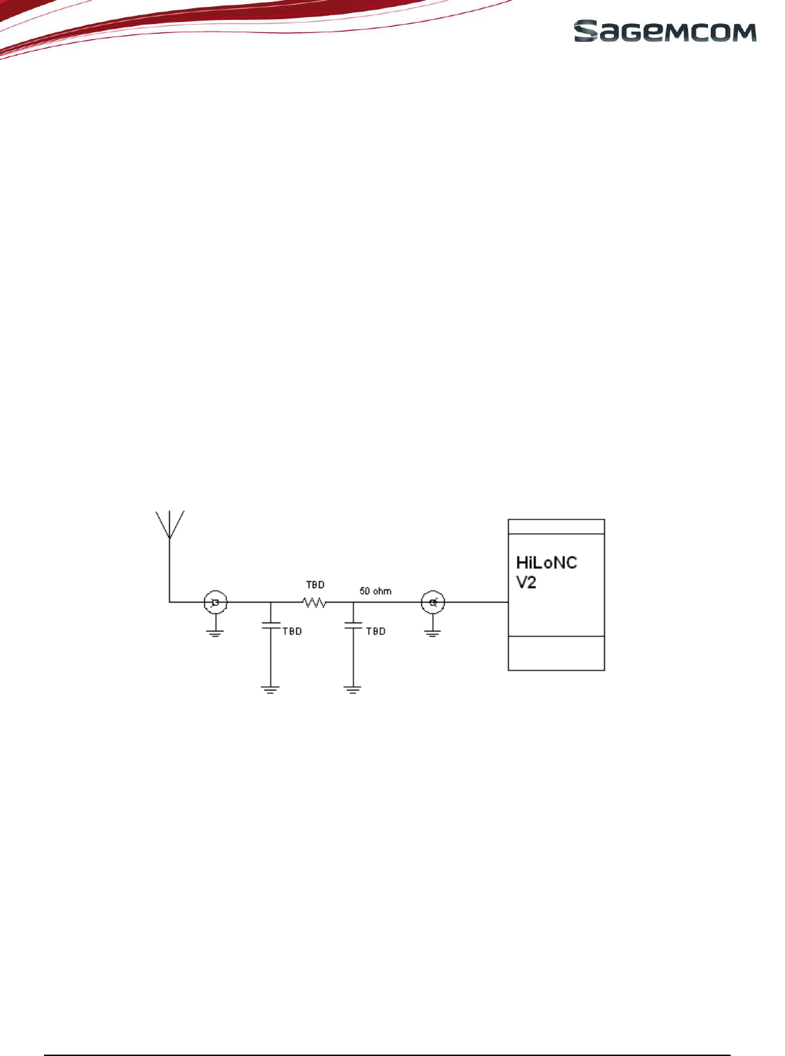
page 43/64
Note d’étude / Technical document : URD1– OTL
5665.3
– 003 / 72238 Edition 01
Document Sagemcom Reproduction et divulgation interdites
Sagemcom document. Reproduction and disclosure prohibited
6.5 Recommendations to avoid ESD issues
Insure good ground connections of the HiLoNC V2 module to the customer’s board.
Flex (if any) shall be shielded and FPC connectors shall be correctly grounded at each extremity.
Put capacitor 100nF on battery, or better put varistor or ESD diode in parallel on battery and charger wires
(if any) and on all power wires connected to the module.
Uncouple microphone and speaker by putting capacitor or varistor in parallel of each wire of these
devices.
7. RADIO INTEGRATION
Note that radio engineering competences are mandatory to get accurate radio performance on customer’s
product.
7.1 ANTENNA
A 50Ω line matching between module and customer’s board, and the RF antenna is required.
Figure 43: Antenna connection
Keep matching circuit on customer’s board but with direct connection in the first step – it could be
necessary to make some adjustment later, during RF qualification stage.
The selected antenna must comply with FCC RF exposure limits in GSM850 and PCS1900 band :
• GSM850 : MPE < 0.55mW/cm
2
(Distance is 20 cm)
• PCS1900 : ERP < 3W
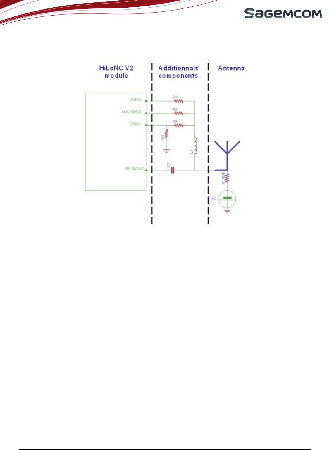
page 44/64
Note d’étude / Technical document : URD1– OTL
5665.3
– 003 / 72238 Edition 01
Document Sagemcom Reproduction et divulgation interdites
Sagemcom document. Reproduction and disclosure prohibited
For antenna detection presence circuit refer to the dedicated document:
URD1 OTL 5365.1 065 71466 ed 01 - Hilo-HiLoNC Antenna Detection
Figure 44: Antenna detection circuit
7.2 GROUND LINK AREA
SAGEMCOM emphasizes the fact that a good ground GND contact is needed between the module and the
customer’s board to have the best radio performances (spurious, sensitivity…).
All HiLoNC V2 GND pads must be connected to the GND of the customer’s board.
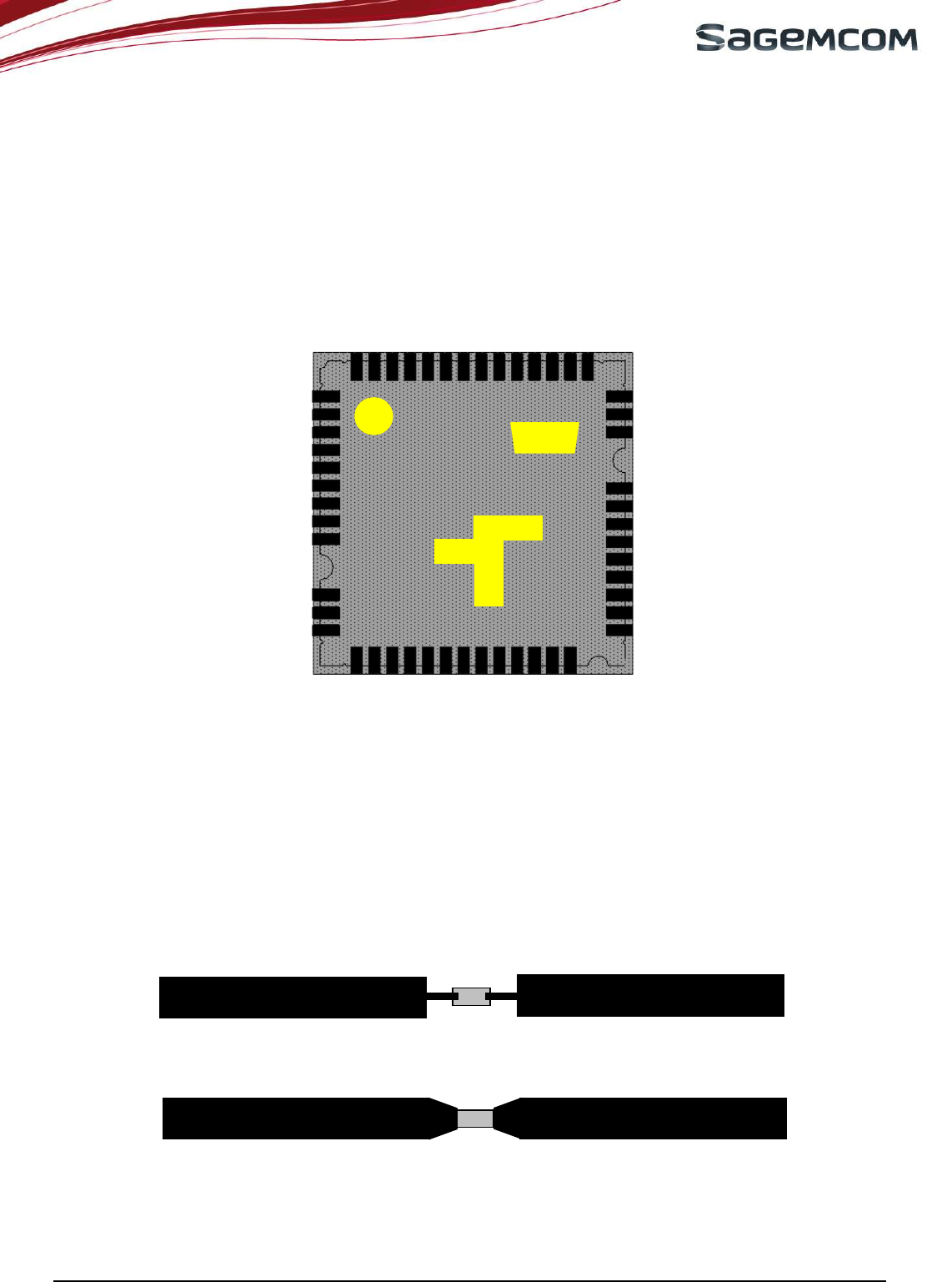
page 45/64
Note d’étude / Technical document : URD1– OTL
5665.3
– 003 / 72238 Edition 01
Document Sagemcom Reproduction et divulgation interdites
Sagemcom document. Reproduction and disclosure prohibited
7.3 LAYOUT
Isolate RF line and antenna from others bus or signals
No signals on 50 ohms area and if that is not possible, add ground shielding using different layers.
Do not add any ground layer under the antenna contact area.
Varnish must be present on all the grey area of the customer's board (expect solder pads) to isolate
HiLoNC V2 module from the customer’s board
Figure 45: Mandatory area for varnish
This recommendation is due to the presence of signals (below varnish) and fiducials and golden tests
points and UL PCB marking (without varnish area in Yellow on the picture above) on the back side of the
module. If customer’s board has layout or via without varnish below the HiLoNC V2 module, short-circuits
could occur between them.
Free CAD software can be used to compute the stack-up parameter that leads to a compliant 50Ω RF
track.
Connection between two RF tracks of different widths or of a FR line with a smaller pad component must be
smoothed to keep a correct RF adaptation.
Figure 46: Connection of RF lines with different width
Not correct
conn
ection
Correct
co
nnection

page 46/64
Note d’étude / Technical document : URD1– OTL
5665.3
– 003 / 72238 Edition 01
Document Sagemcom Reproduction et divulgation interdites
Sagemcom document. Reproduction and disclosure prohibited
7.4 MECHANICAL SURROUNDING
Do not apply mechanical pressure over the HiLoNC V2 shield, this could damage the mechanical
structure of the shield and lead to internal short-circuits or other undesirable issues.
Avoid any metallic part around the antenna area
Keep FPCs and battery contact (if any) far from antenna area.
FPC's (if any) have to be shielded
7.5 OTHER RECOMMENDATIONS – TESTS FOR PRODUCTION/DESIGN
SAGEMCOM guarantees the RF performances in conductive mode but strongly recommends making RF
measurements in an anechoic chamber in radiated mode (tests conditions for FTA): the radiated performances
strongly depend on radio integration (layout, antenna, matching circuit, ground area…..)
8. AUDIO INTEGRATION
Audio mandatory tests for FTA are in handset mode only so a particular care must be brought to the design of
audio (mechanical integration, gasket, electronic) in this mode.
The audio norms which describe the audio tests are 3GPP TS 26.131 & 3GPP TS 26.132.
Note that acoustic competences are mandatory to get accurate audio performance on customer’s product.
8.1 MECHANICAL INTEGRATION AND ACOUSTICS
Particular care to Handset Mode:
To get a better audio output design (speaker part):
The speaker must be completely sealed on front side.
The front aperture must be compliant with speaker supplier’s specifications
The back volume must be completely sealed.
The sealed back volume must be compliant with speaker supplier’s specifications
Take care of the design of the speaker gasket (elastomer).
Foresee a stable and large enough area for the gasket of the artificial ear.
To get a better audio input design (microphone part):
Take care of the design of the microphone (elastomer).
All receivers must be completely sealed on front side.
Microphone sensitivity depends on the shape of the device e.g. about –40 ±3 dBV/Pa.
Promote the use of pre-amplified microphone. If needed, use a pre-amplification stage.

page 47/64
Note d’étude / Technical document : URD1– OTL
5665.3
– 003 / 72238 Edition 01
Document Sagemcom Reproduction et divulgation interdites
Sagemcom document. Reproduction and disclosure prohibited
As audio input and output are strongly linked:
Place the microphone and the speaker as far as possible from one another.
8.2 ELECTRONICS AND LAYOUT
Avoid Distortion & Burst noise
Audio signals must be symmetric (same components on each path).
Differential signals must be routed parallel.
Audio layer must be surrounded by 2 ground layers.
The link from one component to the ground must be as short as possible.
If possible separate the PCB of the microphone and the one of the speaker.
Reduce as much as possible the number of electronics components (loss of quality, more dispersion).
Audio tracks must be larger than 0.5 mm.
9. RECOMMENDATIONS ON LAYOUT OF CUSTOMER’S BOARD
9.1 GENERAL RECOMMENDATIONS ON LAYOUT
There are many different types of signals in the module which are disturbing each other. Particularly, Audio
signals are very sensitive to external signals as VBAT... Therefore it is very important to respect some rules to
avoid disruptions or abnormal behaviour.
Magnetic field generated by VBAT tracks may disturb the speaker, causing audio burst noise. In this case,
modify layout of the VBAT tracks to reduce the phenomena.
9.1.1 Ground
A ground plane as complete as possible
Ground of components has to be connected to the ground layer through many vias not regularly
distributed.
Top and bottom layer shall have as much as possible of ground planes. Flood the empty remain surface
of the layout of those two layers with a ground plane connected to main ground with as much vias as possible.
9.1.2 Power supplies
Layer for power supply signals (VBAT, VGPIO) is recommended.
Any loop of power signals layout must be avoided on the design.
Suitable power supply (VBAT, VGPIO) track width and thickness.

page 48/64
Note d’étude / Technical document : URD1– OTL
5665.3
– 003 / 72238 Edition 01
Document Sagemcom Reproduction et divulgation interdites
Sagemcom document. Reproduction and disclosure prohibited
9.1.3 Clocks
Clock signals must be shielded between two grounds layer and bordered with ground vias.
9.1.4 Data bus and other signals
Data bus and commands have to be routed on the same layer; none of the lines of the bus shall be
parallel to other lines
Lines crossing shall be perpendicular
Suitable other signals track width, thickness.
Data bus must be protected by upper and lower ground plans
9.1.5 Radio
Provide a 50 Ohm micro strip line for antenna connection
9.1.6 Audio
Differential signals have to be routed together, parallel (for example HSET_OUT_P/HSET_OUT_N).
Audio signals have to be isolated, by pair, from all the other signals (ground all around each pair).
Cancel any loops between VBAT and GND next to the speaker to avoid the TDMA burst noise in the
speaker during a communication.
The single-end audio signal should be adopted the same rules as differential signals.
Figure 47: Layout of audio differential signals on a layer n
Figure 48: Adjacent layers of audio differential signals
Layer n-1
Layer n
Layer n+1
GND
HSET_OUT_P
GND
GND
HSET_OUT_P
GND
HSET_OUT_N
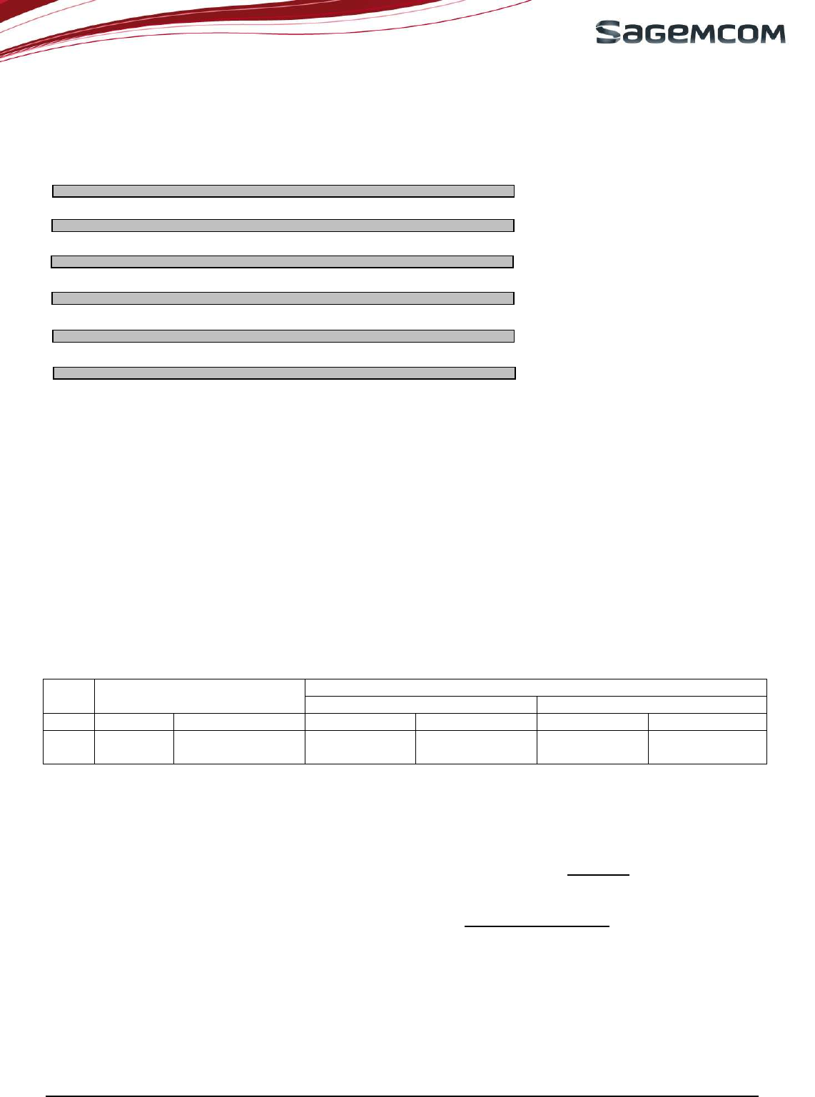
page 49/64
Note d’étude / Technical document : URD1– OTL
5665.3
– 003 / 72238 Edition 01
Document Sagemcom Reproduction et divulgation interdites
Sagemcom document. Reproduction and disclosure prohibited
9.2 EXAMPLE OF LAYOUT FOR CUSTOMER’S BOARD
The following figure shows an example of layer allocation for a 6 layers circuit (for reference only):
Depending on the customer’s design the layout could also be done using 4 layers.
Figure 49: layer allocation for a 6 layers circuit
10. RECOMMANDATIONS FOR CUSTOMER PRODUCTION
Note for following chapters that except where standards are indicated, the given characteristics should be
considered as validated conditions used on SAGEMCOM product.
Other conditions depending of the customer’s factory process are not validated but can be submitted to
SAGEMCOM for proficiency.
10.1 MOISTURE LEVEL
According to IPC/JEDEC J-STD 20, the HiLoNC V2 has the following MSL level: 3
Customer’s module are shipped under a Dry package with all the MSL information labelled.
Soak requirements Level
Floor Life Standard Accelerated Equivalent
Time Conditions Time (hours) Conditions Time (hours) Conditions
3 168
hours <= 30°C/60% RH 192 +5/-0 30°C / 60% RH 40 +1/-0 60° C / 60%RH
It means that the customer’s factory must process and solder the HiLoNC V2 on the customer’s board at least
168 hours (7 days) after the HiLoNC V2 sealed package have been opened. This duration is given for factory
floor conditions of T°<30°C, HR 60%.
If this maximum 7 days duration can not be fulfilled, the HiLoNC V2 part must be baked again.
Unless the factory floor conditions are perfectly controlled, SAGEMCOM does not recommend to wait
until this maximum 7 days duration before soldering the HiLoNC V2 on customer’s board.
For any module exposed to ambient moisture it is therefore highly recommended to proceed to a baking
according to the JEDEC (125°C during 24H) to dry th e module before any soldering process
10.2 PACKAGE
The HiLoNC V2 module is delivered in Tape and Reel package which is hermetically sealed to prevent from
moisture and ESD.
The characteristics of the T&R are given in the drawing below.
Layer 1: Components (HiloNC)
Layer 2: Bus
Layer 3: Power supply
Layer 4: Complete GND layer
Layer 5: Audio, clocks, sensitive signals
Layer 6: GND,test points
page 50/64
Note d’étude / Technical document : URD1– OTL
5665.3
– 003 / 72238 Edition 01
Document Sagemcom Reproduction et divulgation interdites
Sagemcom document. Reproduction and disclosure prohibited
Figure 50: Factory Tape dimensions
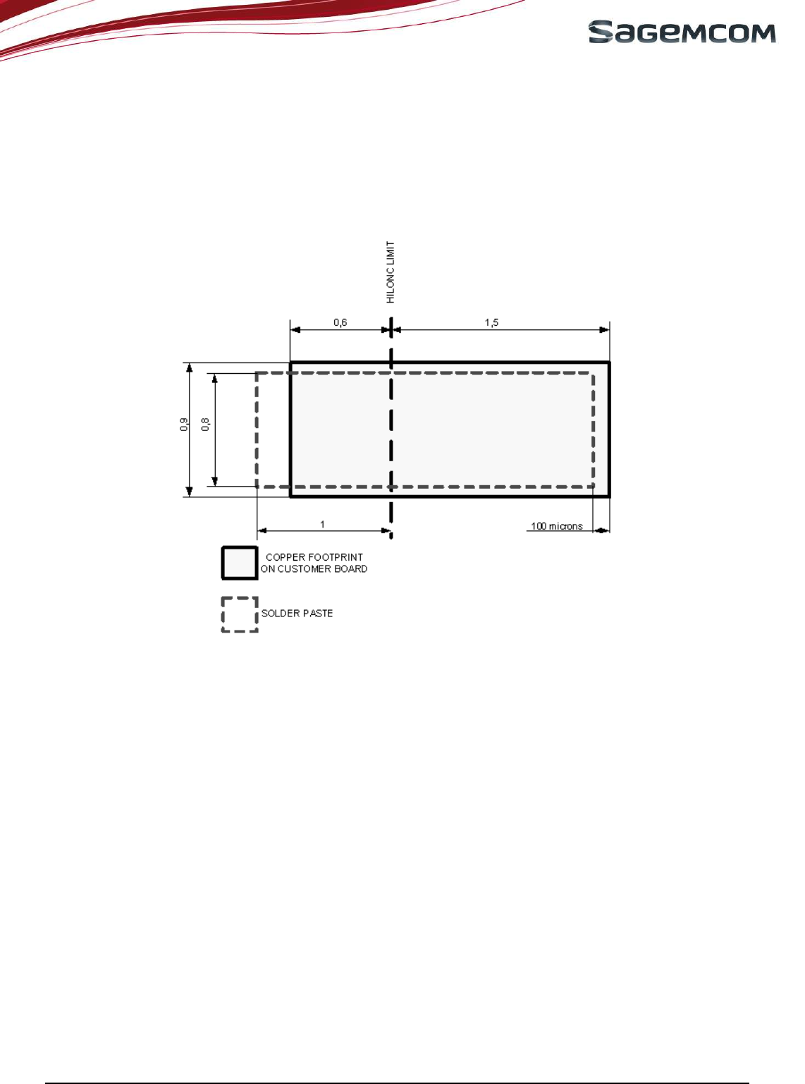
page 51/64
Note d’étude / Technical document : URD1– OTL
5665.3
– 003 / 72238 Edition 01
Document Sagemcom Reproduction et divulgation interdites
Sagemcom document. Reproduction and disclosure prohibited
10.3 STENCIL
Below are given soldering characteristics to report the HiLoNC V2 on the customer’s board.
Copper footprint is shown in solid line on the figure below. Stencil footprint is shown in dotted line.
Note that the opening and the pads do not strictly recover themselves.
Figure 51 : Solder mask design
10.4 SOLDER PASTE
SAGEMCOM recommends a stencil thickness of 135 µm.
SAGEMCOM recommends use of a “no clean” solder paste. Flux cleaning after module soldering on the
customer’s board is not recommended as it can lead to short circuit, label degradation.
Solder paste: M705-GRN360-K-V (Senju Metal Industry Co., Ltd.)
Alloy composition: Sn96.5-Ag3.0-Cu0.5
Melting temperature: solidus 216°C / Peak 217°C / liquidus 220°C
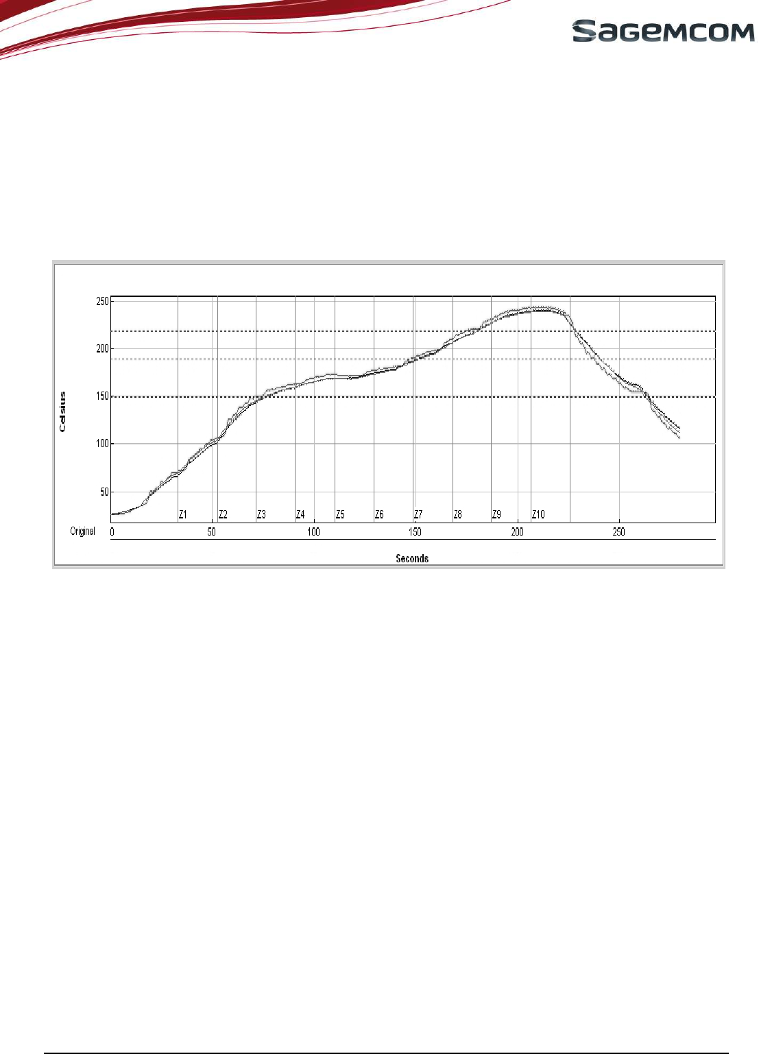
page 52/64
Note d’étude / Technical document : URD1– OTL
5665.3
– 003 / 72238 Edition 01
Document Sagemcom Reproduction et divulgation interdites
Sagemcom document. Reproduction and disclosure prohibited
10.5 PROFILE FOR REFLOW SOLDERING
A convection type soldering oven is recommended.
Typical usable profile is shown on the next figure. The final profile has to be tuned depending on other elements
like solder paste, customer’s board, other components…
Peak temperature: 245°C
Average ramp up rate: 3°C/second max
Average ramp dacay rate: 3°C/second max
Figure 52 : Typical thermal profile
The HiLoNC V2 module is a Lead-free product which has been validated integrated in a lead-free product, using
a lead-free factory process.
No test has been performed using a leaded process. SAGEMCOM does not recommend using a factory
leaded process and does not guarantee any reliable result on the final product.
10.6 SMT MACHINE
HiLoNC V2 is a compact postage stamp sized module optimized for use with pick-and-place machines.
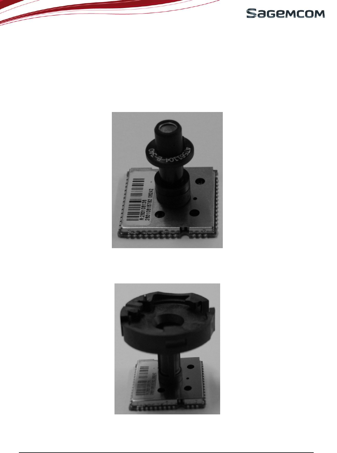
page 53/64
Note d’étude / Technical document : URD1– OTL
5665.3
– 003 / 72238 Edition 01
Document Sagemcom Reproduction et divulgation interdites
Sagemcom document. Reproduction and disclosure prohibited
10.6.1 Nozzles
SAGEMCOM recommends using SMT machine with nozzle diameters up to 8 mm in order to always have
best prehension of the HiLoNC V2 module.
SAGEMCOM recommends using the following two references of nozzles:
• For the UNIVERSAL GSM FLEXJET the nozzle 340F
Figure 53 : Flexjet nozzle 340F
• For the SIEMENS, the nozzle type 417
Figure 54 : Siemens nozzle 417
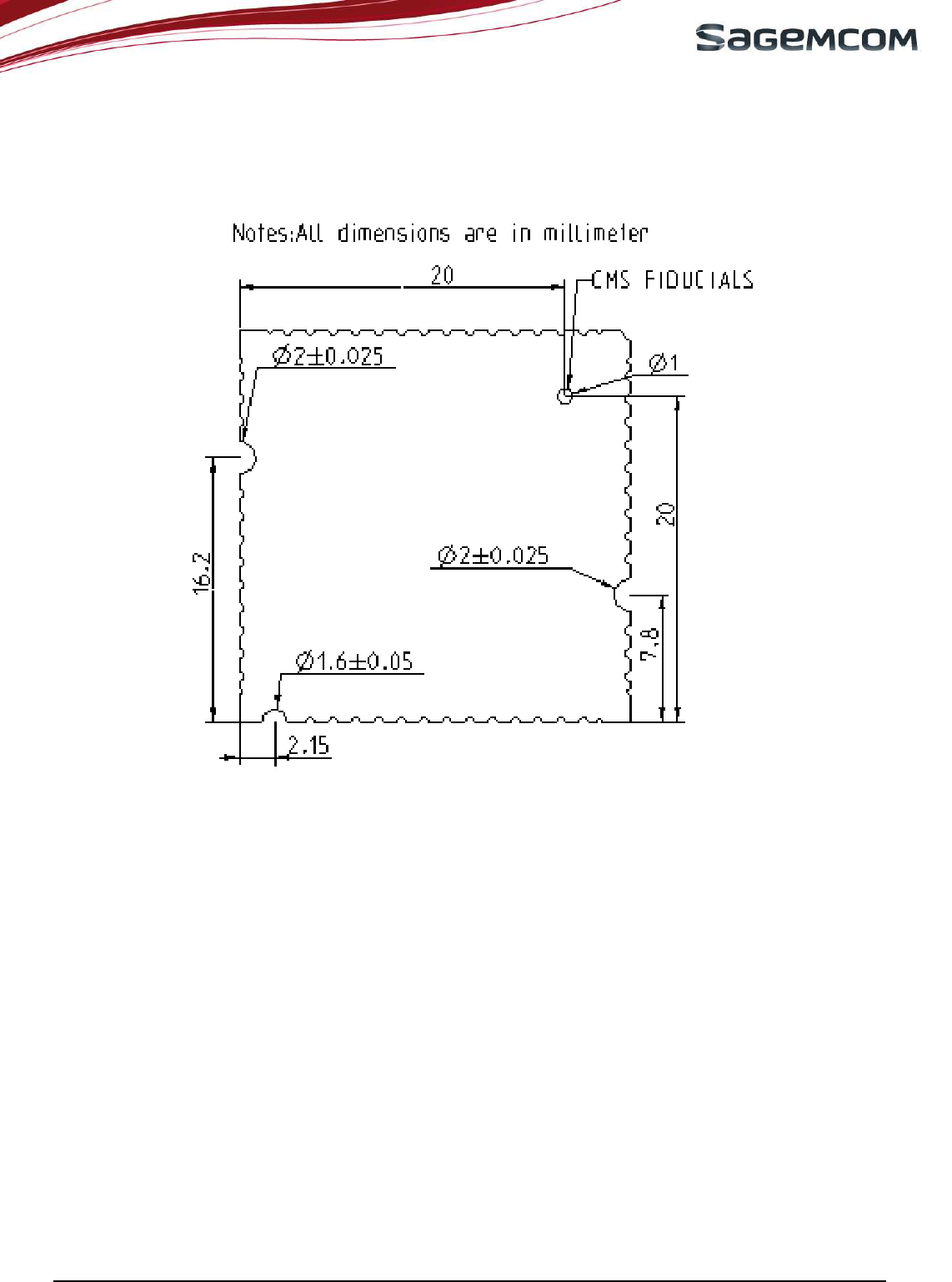
page 54/64
Note d’étude / Technical document : URD1– OTL
5665.3
– 003 / 72238 Edition 01
Document Sagemcom Reproduction et divulgation interdites
Sagemcom document. Reproduction and disclosure prohibited
10.6.2 Fiducials
Optical inspection for placement is possible with SMD fiducials placed on the bottom side of the HiLoNC V2.
SMD fiducials are not symmetrical in order to help optical inspection to define the right orientation.
Figure 55 : Fiducials positions
10.7 UNDERFILL
Despite its important reliability, some customer could request for some specific and extreme applications the
underfill of onboard components.
The HiLoNC V2’s shield has be designed accordingly to allow this process, as shown in the figure below.
More details will be given in a specific application note.
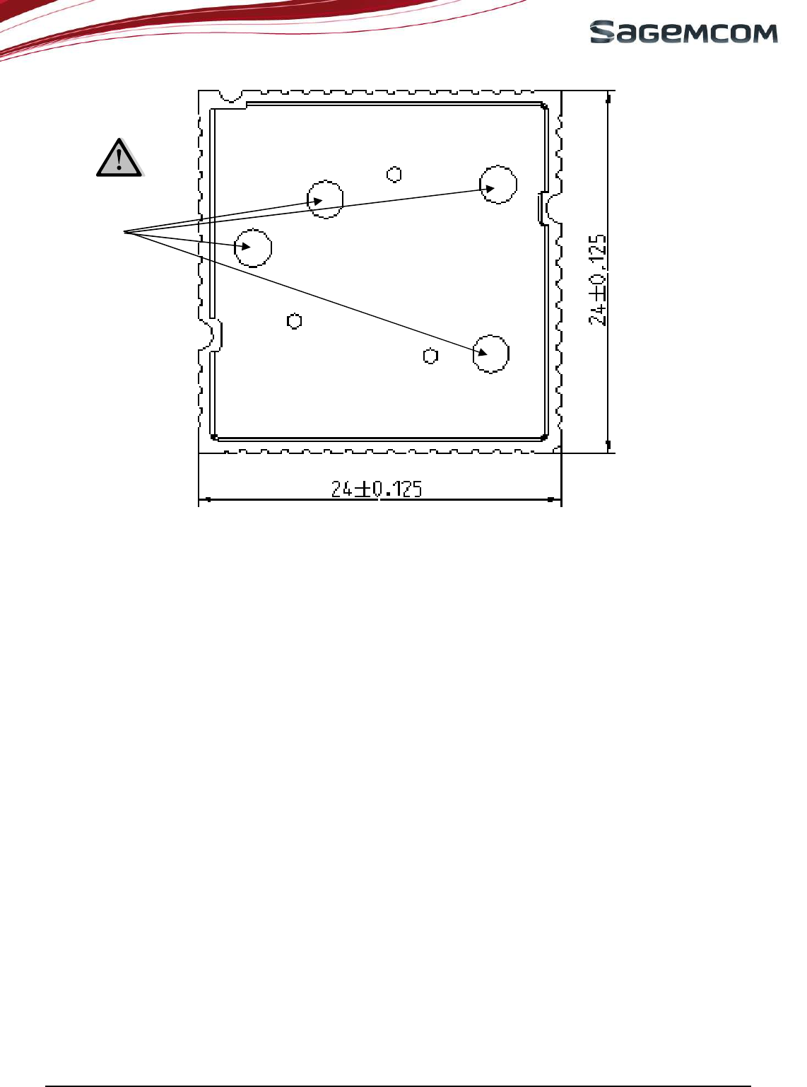
page 55/64
Note d’étude / Technical document : URD1– OTL
5665.3
– 003 / 72238 Edition 01
Document Sagemcom Reproduction et divulgation interdites
Sagemcom document. Reproduction and disclosure prohibited
Figure 56 : Underfill injection holes
10.8 SECOND REFLOW SOLDERING
Even if SAGEMCOM recommends a single reflow soldering, a second reflow soldering can be conceivable (only
if underfill has not been already performed). Positive tests have been performed with HiLoNC V2 on the bottom
side.
Second reflow soldering is not possible if HiLoNC V2 module has been already under filled.
10.9 HAND SOLDERING
Hand soldering is possible.
An especial care must be considered to properly position the HiLoNC V2 on its copper footprint during
hand soldering. Begin with pads diagonally opposite to help in proper positioning.
10.10 UNSOLDERING
Manual unsoldering is possible, for repair purpose for example.
A special care must be considered in order to avoid overheating the HiLoNC V2.
For repairing: Usage of hot plate like example below can be considered with additional metallic cubic plate
whose dimensions are HiLoNC V2's ones (to heat only HiLoNC V2 surface)
Underfill Injection
Holes

page 56/64
Note d’étude / Technical document : URD1– OTL
5665.3
– 003 / 72238 Edition 01
Document Sagemcom Reproduction et divulgation interdites
Sagemcom document. Reproduction and disclosure prohibited
Figure 57 : Laboratory hot plate to unsolder the module
Customer must remember to not have components on the HiLoNC V2 opposite side of the customer’s
board.
11. LABEL
The HiLoNC V2 module is labelled with its own FCC ID(TBD) on the shield side. When the module is installed in
customer’s product, the FCC ID label on the module will not be visible. To avoid this case, an exterior label must
be stuck on the surface of customer’s product signally to indicate the FCC ID of the enclosed module. This label
can use wording such as the following: “Contains Transmitter module FCC ID: TBD” or “Contains FCC ID:
TBD”.
Electronic board
HiLoNC
Cube to
concentrate
the heat Unsoldering hot
plate
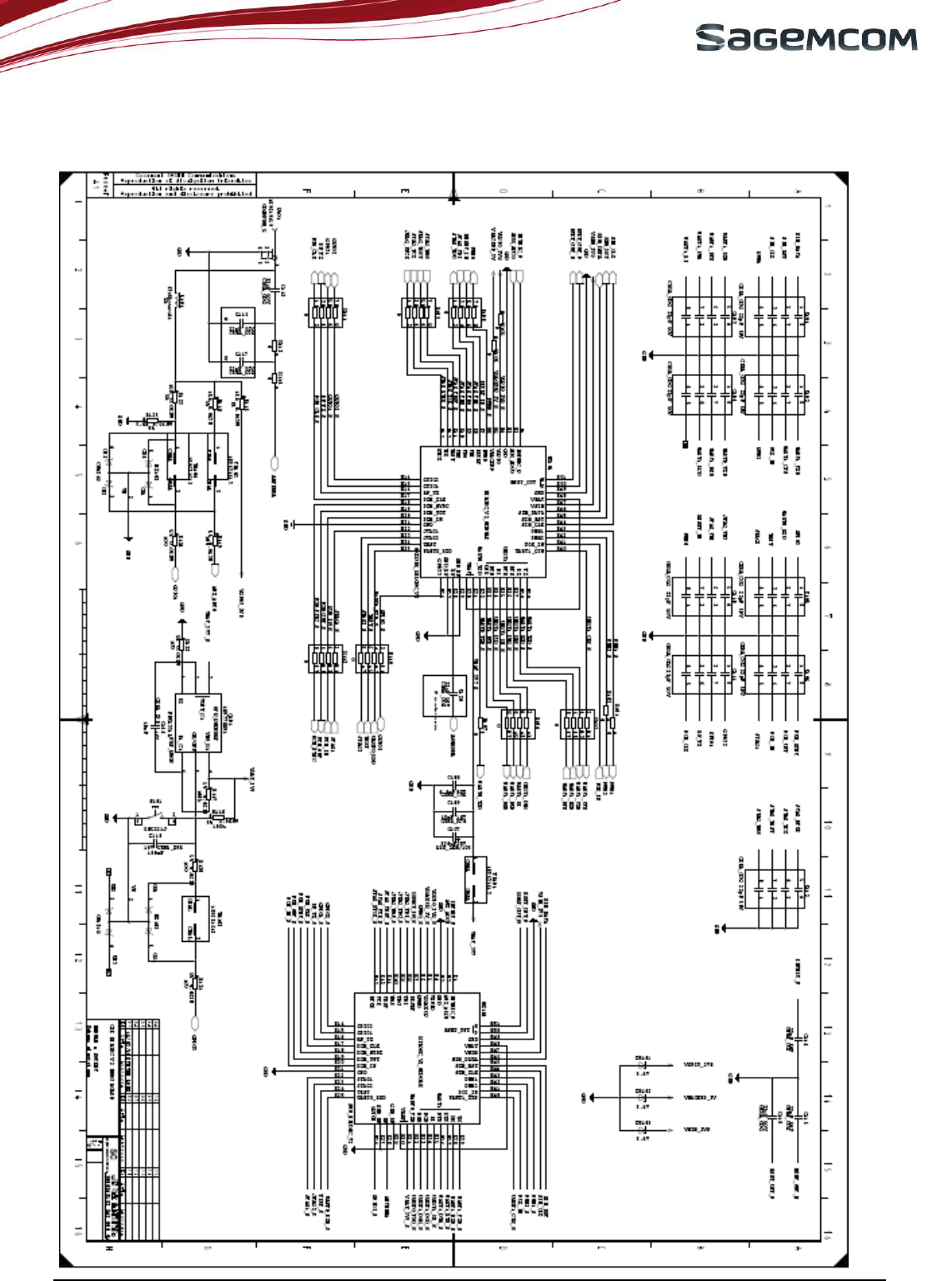
page 57/64
Note d’étude / Technical document : URD1– OTL
5665.3
– 003 / 72238 Edition 01
Document Sagemcom Reproduction et divulgation interdites
Sagemcom document. Reproduction and disclosure prohibited
12. REFERENCE DESIGN: HiLoNC V2 DEVELOPMENT KIT
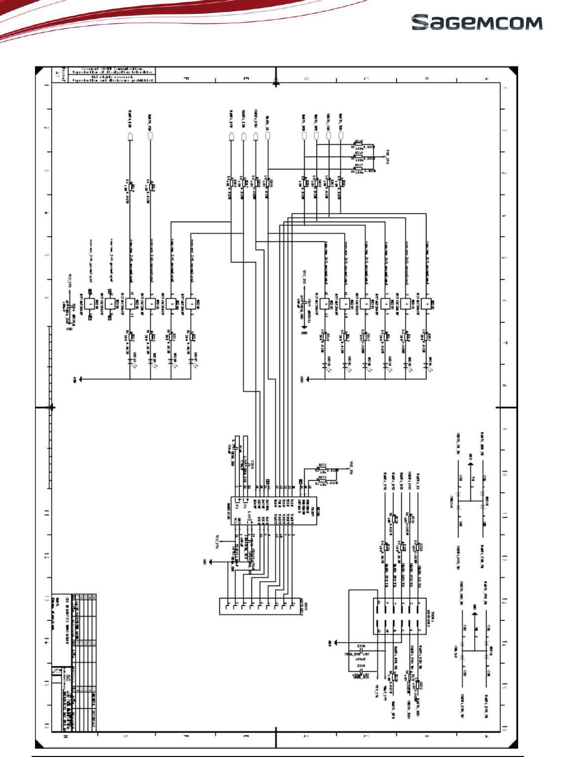
page 58/64
Note d’étude / Technical document : URD1– OTL
5665.3
– 003 / 72238 Edition 01
Document Sagemcom Reproduction et divulgation interdites
Sagemcom document. Reproduction and disclosure prohibited
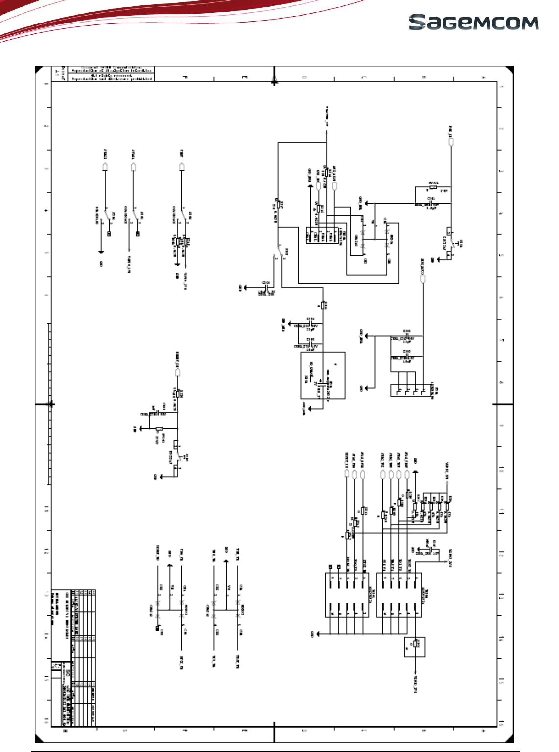
page 59/64
Note d’étude / Technical document : URD1– OTL
5665.3
– 003 / 72238 Edition 01
Document Sagemcom Reproduction et divulgation interdites
Sagemcom document. Reproduction and disclosure prohibited
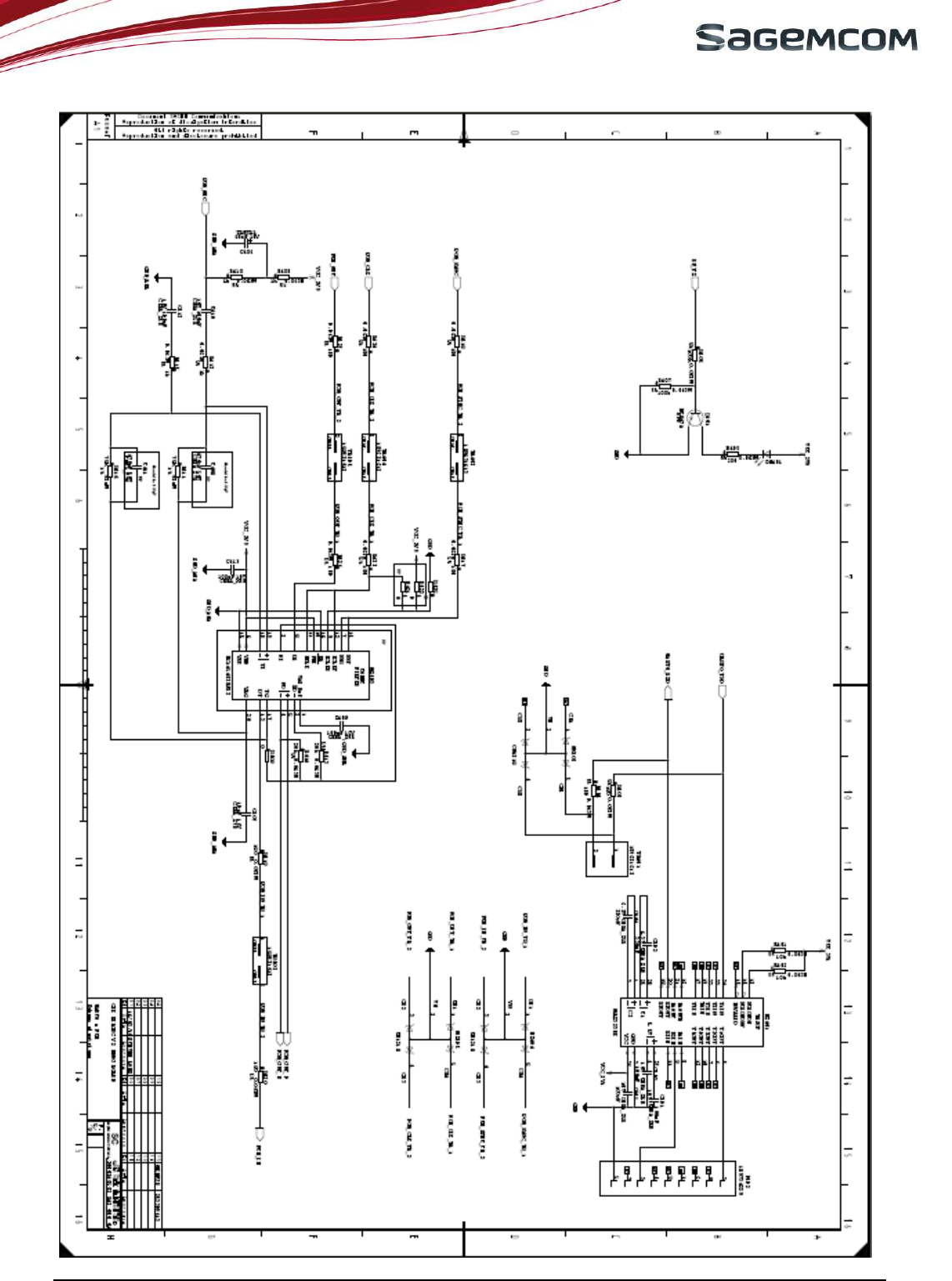
page 60/64
Note d’étude / Technical document : URD1– OTL
5665.3
– 003 / 72238 Edition 01
Document Sagemcom Reproduction et divulgation interdites
Sagemcom document. Reproduction and disclosure prohibited
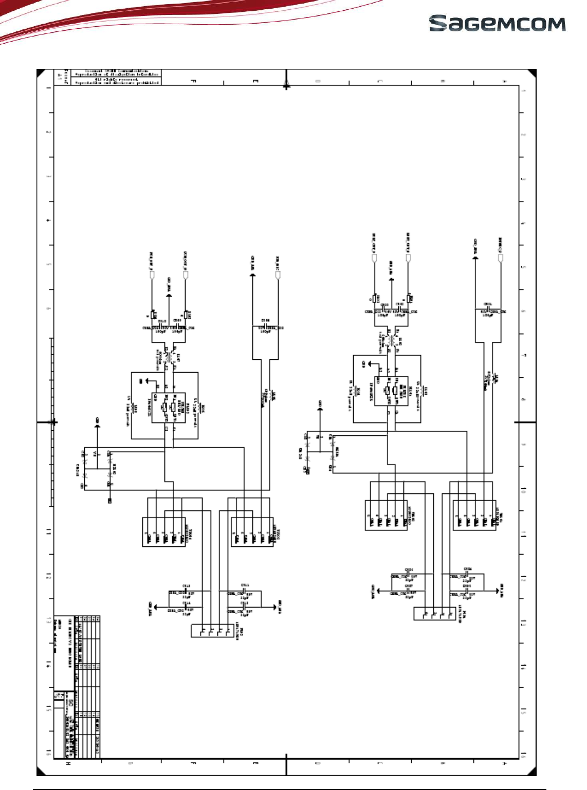
page 61/64
Note d’étude / Technical document : URD1– OTL
5665.3
– 003 / 72238 Edition 01
Document Sagemcom Reproduction et divulgation interdites
Sagemcom document. Reproduction and disclosure prohibited
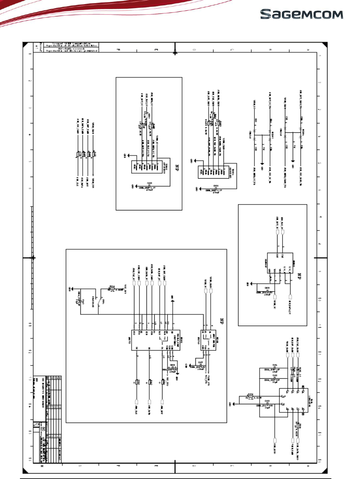
page 62/64
Note d’étude / Technical document : URD1– OTL
5665.3
– 003 / 72238 Edition 01
Document Sagemcom Reproduction et divulgation interdites
Sagemcom document. Reproduction and disclosure prohibited
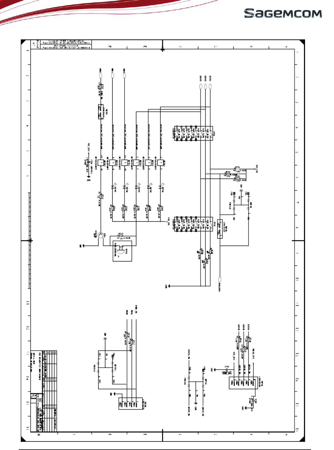
page 63/64
Note d’étude / Technical document : URD1– OTL
5665.3
– 003 / 72238 Edition 01
Document Sagemcom Reproduction et divulgation interdites
Sagemcom document. Reproduction and disclosure prohibited
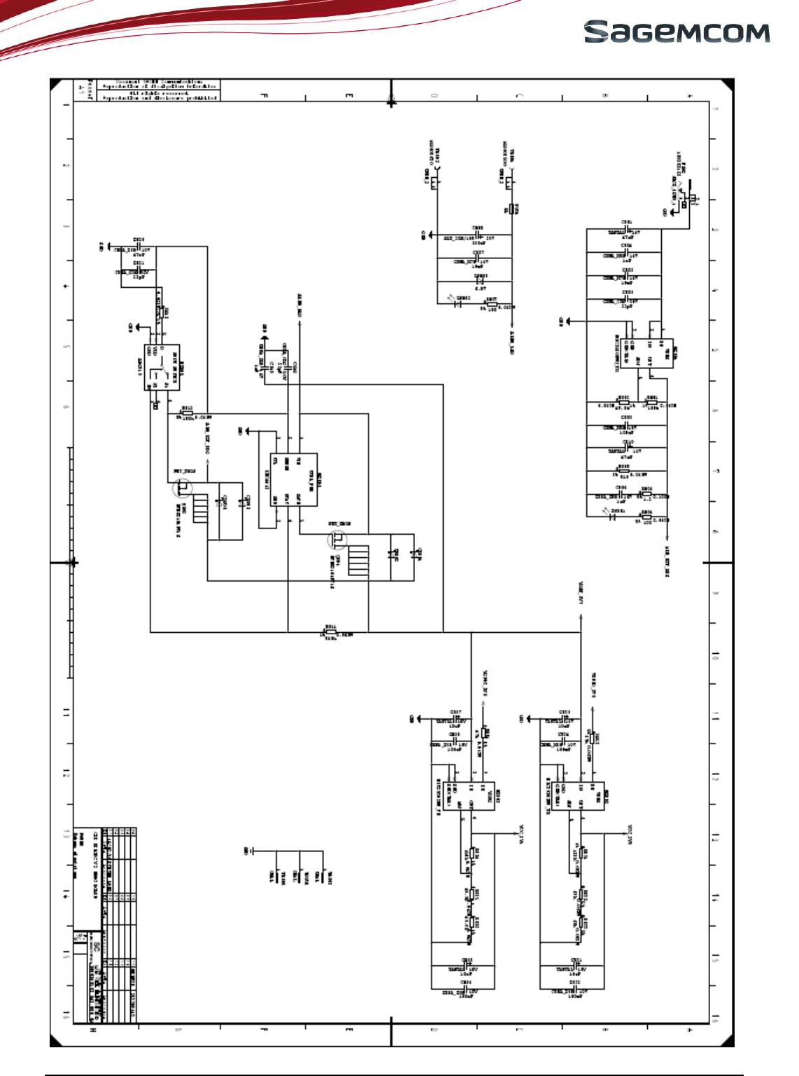
page 64/64
Note d’étude / Technical document : URD1– OTL
5665.3
– 003 / 72238 Edition 01
Document Sagemcom Reproduction et divulgation interdites
Sagemcom document. Reproduction and disclosure prohibited