SAMSUNG DLP Television Manual L0902265
User Manual: SAMSUNG SAMSUNG DLP Television Manual SAMSUNG DLP Television Owner's Manual, SAMSUNG DLP Television installation guides
Open the PDF directly: View PDF ![]() .
.
Page Count: 139 [warning: Documents this large are best viewed by clicking the View PDF Link!]
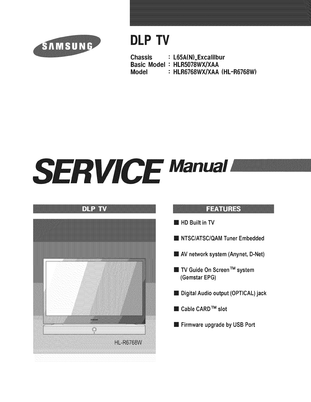
Chassis
Basic Model
Model
• L65A(N)=Excalilbur
• HLRS078WX/XAA
• HLR6768WX/XAA (HL-R6768W)
Manual
HD Built in TV
m NTSC/ATSC/QAM Tuner Embedded
m AV network system (Anynet, D-Net)
mTV Guide On ScreenTMsystem
(Gemstar EPG)
mDigitalAudio output (OPTICAL)jack
m Cable CARDTMslot
m Firmware upgrade by USB Port
Tableof Contents
Chapter 1 Precaution
1-1SafetyPrecautions........................................................... 1-1
m 1-2ServicingPrecautions ........................................................ 1-3
m 1-3StaticElectricityPrecautions ................................................... 1-4
m 1-4InstallationPrecautions....................................................... 1-5
Chapter 2 Product Specification
m 2-1 ProductFeatures ............................................................ 2-1
m 2-2 KeyFeatures ............................................................... 2-2
m 2-3SpecificationsAnalysis........................................................ 2-4
m 2-4Accessories ................................................................ 2-5
Chapter 3Alignment & Adjustment
m 3-I ServiceInstruction ........................................................... 3-1
m 3-2 Howto AccessServiceNode ................................................... 3-2
m 3-3 FactoryData................................................................ 3-3
m 3-4ServiceAdjustment .......................................................... 3-15
m 3-5SoftwareUpgrade ........................................................... 3-18
m 3-6 Replacements& Calibration.................................................... 3-19
Chapter 4 Exploded View & Part List
m 4-I HLR6768VVX/XAA........................................................... 4-I
m 4-2 L680EngineAss'y ........................................................... 4-2
Chapter 5 Electrical Part List
m 5-1 HLR6768VVX/XAAServiceItem ................................................. 5-1
Chapter 6 Troubleshooting
m 6-I Checkpointsby ErrorMode .................................................... 6-1
m 6-2TroubleshootingProceduresby ErrorModes....................................... 6-7
m 6-3TroubleshootingProceduresbyASS'Y ........................................... 6-8
Chapter 7 Block Diagram
m 7-1OverallBlockDiagram ........................................................ 7-1
m 7-2 PartialBlockDiagram......................................................... 7-2
Chapter 8 Wiring Diagram
m 8-I OverallWiring ............................................................... 8-1
m 8-2ConnectionbetweenAnalogandDigitalBoard ..................................... 8-2
Chapter9PCBDiagram
m 9-1 PowerBoard ............................................................... 9-1
m 9-2 DigitalBoard................................................................ 9-3
m 9-3AnalogBoard ............................................................... 9-6
m 9-4 DMDBoard................................................................ 9-9
Chapter 10 Schematic Diagram
m 10-1AnalogBoard .............................................................. 10-I
m 10-2DigitalBoard............................................................... 10-10
m 10-3DMD ..................................................................... 10-28
m 10-4Power .................................................................... 10-39
m 10-5Detect.................................................................... 10-40
m 10-6PowerLED ................................................................ 10-41
m 10-7RMC ..................................................................... 10-42
Chapter 11 Operation instruction &installation
m 11-1ProductFeaturesandFunctions ............................................... 1I-1
m 1I-2 NewFeatures.............................................................. 1I-5
Chapter 12 Disassembly & Reassembly
m 12-1OverallDisassembly& Reassembiy ............................................ 12-1
Chapter 13 Circuit Description
m 13-I OverallBlockDescription..................................................... 13-1
m 13-2PartialBlockDescription ..................................................... 13-2
m 13-3NewCircuitDescription ...................................................... 13-7
Chapter 14 Reference information
m 14-I Otherissuesrelatedto other products........................................... 14-I
m 14-2TechnicalTerms ............................................................ 14-3
Precaution
1. Precaution
Toavoidpossibledamagesor electricshocksor exposureto radiation,followthe instructionsbelowwith regardto safety,
installation,serviceand ESD.
1-1Safety Precautions
,
,
Makesureall protectivedevicesare properlyinstalled
includingnon-metallichandlesandcompartmentcovers
wheninstallingor re-installingthe chassisor chassis
assemblies.
Makesurethatno gapsexist betweenthe cabinetsfor
childrento inserttheirfingersin to preventchildrenfrom
receivingelectricshocks.
Errorsmayoccurwhenthe resistanceis below1.0 M_or
over 5.2 M_.
Inthesecases, makesure thatthe deviceis repaired
beforesendingit backto the customer.
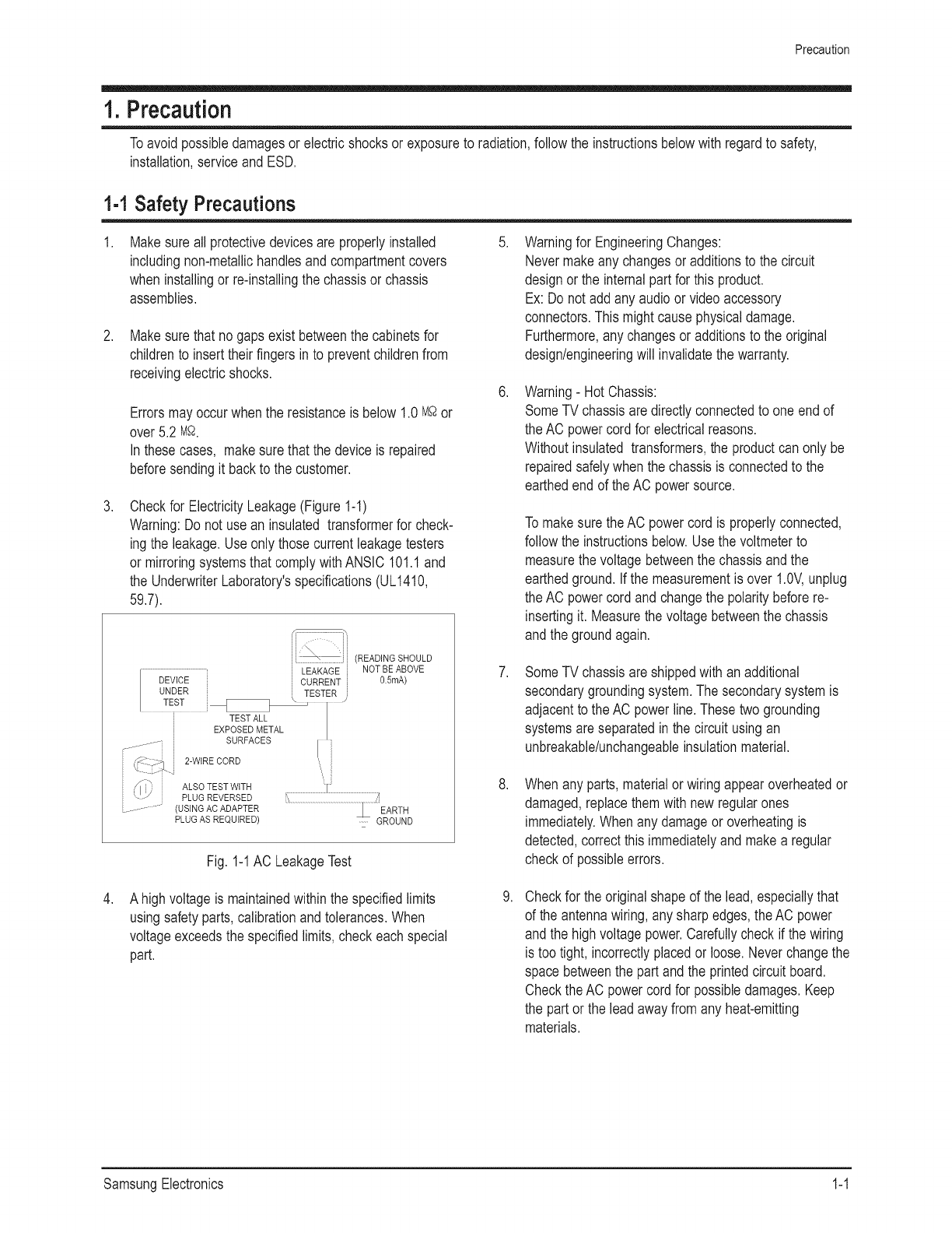
Checkfor ElectricityLeakage(Figure 1-1)
Warning:Donot use an insulatedtransformerfor check-
ingthe leakage.Useonly thosecurrentleakagetesters
or mirroringsystemsthatcomplywithANSIC 101.1and
the UnderwriterLaboratory'sspecifications(UL1410,
59.7).
LEAKAGE
DEVICE CURRENT
UNDER \ TESTER
i TEST ALL I
i EXPOSED METAL
..............i SURFACESi
2-WIRE CORD
ALSO TEST WtTH
PLUG REVERSED
...... -- ' (USING AC ADAPTER
PLUG AS REQUIRED)
(READING SHOULD
NOT BE ABOVE
0.5mA)
........GROUND
Fig.1-1AC LeakageTest
,
,
Warningfor EngineeringChanges:
Nevermakeany changesor additionsto the circuit
designorthe internalpartfor this product.
Ex: Do notaddany audioor videoaccessory
connectors.Thismightcausephysicaldamage.
Furthermore,anychangesor additionsto theoriginal
design/engineeringwill invalidatethe warranty.
Warning- HotChassis:
SomeTV chassisaredirectlyconnectedto oneendof
theAC powercordfor electricalreasons.
Withoutinsulated transformers,the productcanonly be
repairedsafelywhen thechassisis connectedto the
earthedend of theAC powersource.
TomakesuretheAC powercord is properlyconnected,
followthe instructionsbelow.Usethe voltmeterto
measurethe voltagebetweenthe chassisandthe
earthedground.If the measurementis over 1.0V,unplug
theAC powercord andchangethe polaritybeforere-
insertingit. Measurethe voltagebetweenthe chassis
andthe groundagain.
SomeTV chassisareshippedwithan additional
secondarygroundingsystem.Thesecondarysystemis
adjacentto theAC powerline.Thesetwogrounding
systemsareseparatedin the circuitusingan
unbreakable/unchangeableinsulationmaterial.
Whenany parts,materialor wiringappearoverheatedor
damaged,replacethemwithnew regularones
immediately.Whenany damageor overheatingis
detected,correctthisimmediatelyand makea regular
checkof possibleerrors.
,A highvoltageis maintainedwithinthe specifiedlimits
usingsafetyparts,calibrationand tolerances.When
voltageexceedsthe specifiedlimits,checkeachspecial
part.
,Checkfor the originalshapeof the lead,especiallythat
of the antennawiring,anysharpedges,the AC power
andthe highvoltagepower.Carefullycheck if the wiring
is too tight, incorrectlyplacedor loose.Neverchangethe
spacebetweenthe partand the printedcircuitboard.
ChecktheAC powercordfor possibledamages.Keep
the partor the leadawayfromany heat-emitting
materials.
SamsungElectronics 1-1
Precaution
10.
11.
SafetyIndication:
Someelectricalcircuitsor devicerelatedmaterials
requirespecialattentionto their safetyfeatures,which
cannotbe viewedby the nakedeye.If anoriginalpart is
replacedwithanotherirregularone,the safetyor
protectivefeatureswill be losteven if the newone hasa
highervoltageor morewatts.
Criticalsafetypartsshouldbebracketedwith _ Z_ ).
Useonly regularpartsfor replacements(in particular,
flameresistanceand dielectricstrengthspecifications).
Irregularpartsor materialsmaycauseelectricshockor
fire.
Payadditionalattentionto the currentleakageas the
voltagebetweenthe powerboardandthe ballastis 220
to 440v,i.e. veryhigh.
Andalso bewareof possibleelectricshockfromthe
primarypowersource.
1-2 SamsungElectronics
Precaution
1-2Servicing Precautions
Warning1: Firstcarefullyreadthe "Safety Instruction"inthisservicemanual,
Whenthereis a conflictbetweenthe serviceandthe safetyinstructions,followthe safetyinstructionat all times,
Warning2:Any electrolyticcapacitorwiththe wrongpolaritywill explode,
,
,
,
,
The serviceinstructionsare printedon the cabinet,and
shouldbefollowedby any servicepersonnel,
Makesureto unplugtheAC powercordfromthe power
sourcebeforestartingany repairs,
(a) Removeorre-installpartsor assemblies,
(b) Disconnectthe electricplugor connector,if any,
(c) Connectthe test partin parallelwiththe electrolytic
capacitor.
Somepartsareplacedat a higherpositionthan the
printedboard.Insulatedtubesortapesare usedfor this
purpose.The internalwiringis clampedusing bucklesto
avoidcontactwithheat emittingparts,Thesepartsare
installedbackto theiroriginalposition.
Afterthe repair,makesureto checkif the screws,parts
or cablesare properlyinstalled.Makesure nodamageis
causedto the repairedpartand itssurroundings,
Checkfor insulationbetweenthe bladeof the AC plug
andthatof anyconductivematerials(i,e,the metal
panel,inputterminal,earphonejack, etc),
6, InsulationCheckProcess:Unplugthe powercord from
theAC sourceand turnthe switchon. Connectthe insu-
latingresistancemeter(500v)to the AC plugblade,
The insulatingresistancebetweenthe bladeof theAC
plugandthatof the conductivematerialshouldbemore
than 1 M_,
7, Any B+interlockshouldnot be damaged,
If the metalheatsinkis not properlyinstalled,no
connectionto theAC powershouldbemade,
,Makesurethe groundingleadof the testeris connected
to the chassisgroundbeforeconnectingto the positive
lead.The groundleadof the testershouldberemoved
last.
9, Bewareof risksof any currentleakagecominginto
contactwiththe high-capacitycapacitor,
10, The sharpedgesof the metalmaterialmaycause
physicaldamage,so ensurewearingprotectivegloves
duringthe repair.
SamsungElectronics 1-3

Precaution
1-3Static Electricity Precautions
,
,
,
Somesemi-conductive("solidstate")devicesare
vulnerableto staticelectricity.Thesedevicesare known
as ESD.ESDincludesthe integratedcircuitandthefield
effecttransistor.To avoidanymaterialsdamagefrom
electrostaticshock,followthe instructionsdescribed
below.
Removeany staticelectricityfromyour bodyby
connectingthe earthgroundbeforehandlingany
semi-conductivepartsor ass'ys.Alternatively,weara
dischargeablewrist-belt.
(Makesure to removeany staticelectricitybefore
connectingthe powersource- this is a safetyinstruction
for avoidingelectricshock)
Removethe ESDass'yand placeit on a conductive
surfacesuchas aluminumfoil to preventaccumulating
staticelectricity.
,
,
g,
Useonly anti-staticsolderremovaldevices.
Mostsolderremovaldevicesdo not supportan
anti-staticfeature.A solderremovaldevicewithoutan
anti-staticfeaturecan storeenoughstaticelectricityto
causedamageto the ESD.
Do not removethe ESDfromthe protectivebox untilthe
replacementis ready.MostESD replacementsare
coveredwith lead,whichwill causea shortto the entire
unit dueto the conductivefoam,aluminumfoil or other
conductivematerials.
Removethe protectivematerialfrom the ESD
replacementleadimmediatelyafterconnectingit to the
chassisor circuitass'y.
Takeextremecautionin handlingany uncoveredESD
replacements.Actionssuchas brushingclothesor lifting
Donot use any Freon-basedchemicals.
Suchchemicalswill generatestaticelectricitythat
causesdamageto the ESD.
5. Useonly grounded-tipironsfor solderingpurposes.
your legfromthe carpetfloorcan generateenoughstatic
electricityto damagethe ESD.
CAUTION
Theseservicinginstructionsarefor use by
qualifiedservicepersonnelonly.
Toreducethe riskof electricshockdo not
performany servicingotherthanthatcontainedinthe
operatinginstructionsunlessyou arequalifiedto do so.
1-4 SamsungElectronics

Precaution
1-4 Installation Precautions
,
,
,
Forsafetyreasons,morethan twopeopleare required
for carryingthe product.
Keepthe powercord awayfromany heat emitting
devices,as a meltedcoveringmaycausefire orelectric
shock.
Wheninstallingthe product,makesureto keepit away
fromthewall (morethan 10cm/4inches)for ventilation
purposes.
Poorventilationmaycausean increasein the internal
temperatureof the product,resultingin ashortened
componentlife anddegradedperformance.
,
,
Makesureto turn the poweroffand unplugthe power
cordfromthe outletbeforerepositioningthe product.
Alsocheckthe antennacable orthe externalconnectors
if theyare fullyunplugged.Damageto the cordmay
causefire or electricshock.
Keeptheantennafar awayfromany high-voltagecables
andinstallit firmly.Contactwiththe high-voltagecableor
the antennafallingover maycausefire or electricshock.
Whenconnectingthe RFantenna,checkfor a DTV
receivingsystemandinstalla separateDTVreception
antennafor areaswithno DTVsignal.
Checkthe basicsof the screentest.
- Imageposition/size,Tilt adjustment,Actuatoractivation
Bendthe externalantennacablewhen connectingit to
the product.Thisis a measureto protectit frombeing
exposedto moisture.Otherwise,it maycausea fire or
electricshock.
SamsungElectronics 1-5
Product Specification
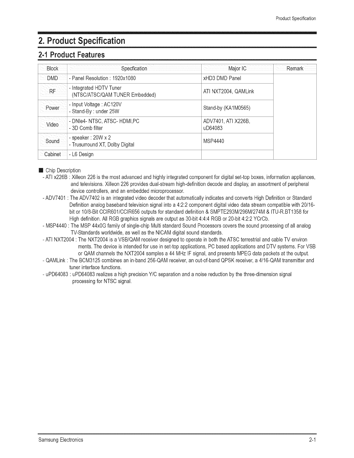
2. ProductSpecification
2-1 Product Features
Block I SpeCfication I Major tC I Remark
DMD- PanelResolution' 1920x1080
-Integrated HDTVTuner
RE (NTSC/ATSC/QAMTUNEREmbedded)
Power '- InputVoltageAC120V
- Stand-By under25W
- DNle4-NTSC,ATSC-HDMI,PC
Video - 3D Combfilter
sOUnd- speaker' 20Wx 2
- TrusurroundXT,DolbyDigital
Cabinet L6Design
xHD3DMD Panel
ATINXT2004,QAMLink
Stand-by(KA1M0565)
ADV7401,ATIX226B,
uD64083
MSP4440
ChipDescription
- ATIx226B: Xilleon226is the most advancedand highlyintegratedcomponentfor digitalset-topboxes,informationappliances,
andtelevisions.Xilleon226 providesdual-streamhigh-definitiondecodeanddisplay,anassortmentof peripheral
devicecontrollers,andan embeddedmicroprocessor.
- ADV7401: The ADV7402is an integratedvideodecoderthatautomaticallyindicatesandconvertsHigh Definitionor Standard
Definitionanalogbasebandtelevisionsignal intoa 4:2:2componentdigitalvideodata streamcompatiblewith20/16-
bit or 10/8-BitCCIR601/CCIR656outputsfor standarddefinition& SMPTE293M/296M/274M& ITU-R.BT1358for
Highdefinition.All RGBgraphicssignalsareoutputas 30-bit4:4:4 RGBor 20-bit4:2:2YCrCb.
- MSP4440: The MSP44x0Gfamilyof single-chipMultistandardSoundProcessorscoversthe soundprocessingof all analog
TV-Standardsworldwide,as well as the NICAMdigitalsoundstandards.
- ATINXT2004: The NXT2004is a VSB/QAMreceiverdesignedto operatein boththe ATSCterrestrialandcableTV environ
ments.Thedeviceis intendedfor use inset-topapplications,PCbasedapplicationsandDTVsystems.ForVSB
or QAMchannelsthe NXT2004samplesa 44 MHz IFsignal,andpresentsMPEGdata packetsat the output.
- QAMLink: The BCM3125combinesan in-band256-QAMreceiver,an out-of-bandQPSKreceiver,a 4/16-QAMtransmitterand
tunerinterfacefunctions.
- uPD64083: uPD64083realizesa highprecisionY/Cseparationanda noise reductionby the three-dimensionsignal
processingfor NTSCsignal.
SamsungElectronics 2-1
Product Specification
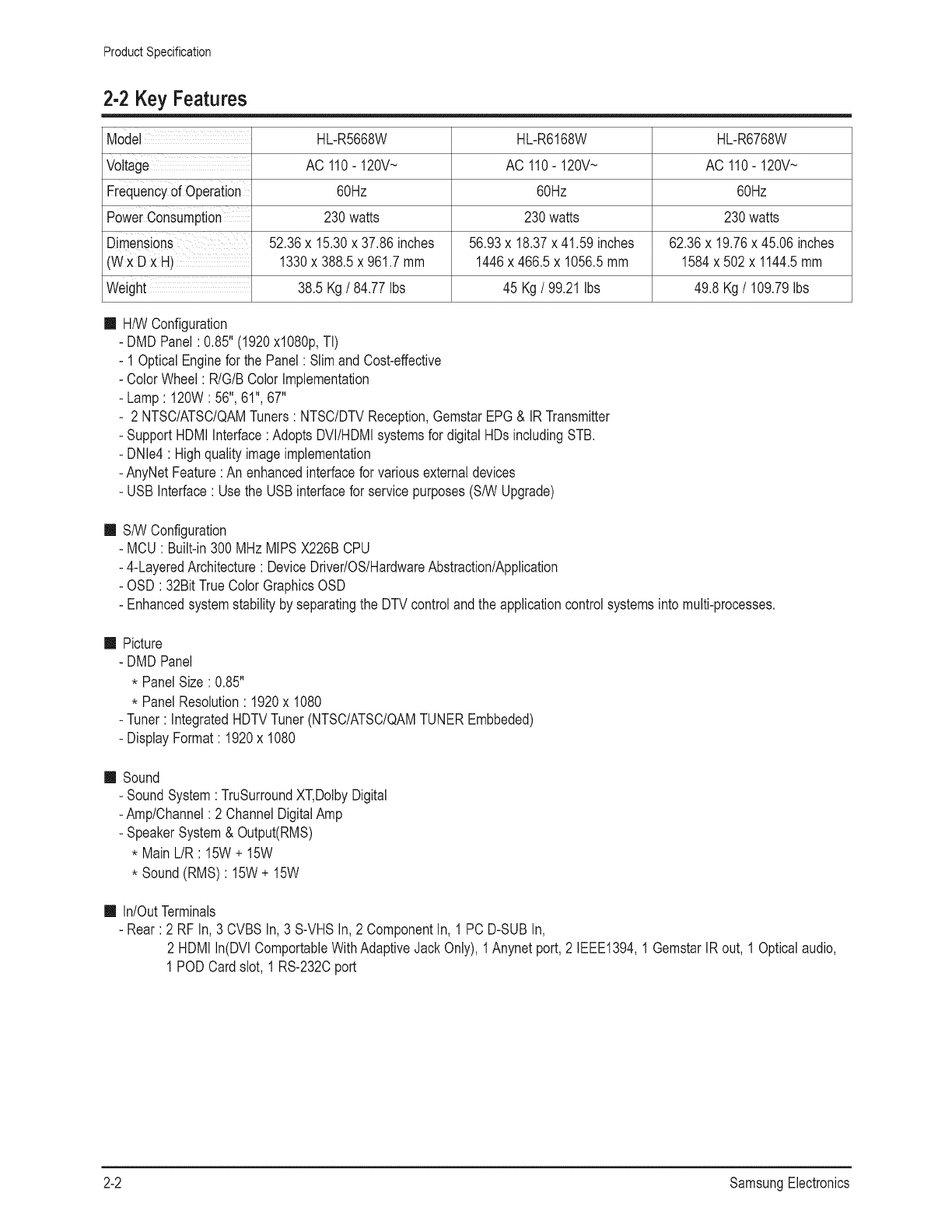
2-2 Key Features
Model HL-R5668W HL-R6168W HL-R6768W
Voltage AC 110- 120V~ AC 110- 120V~ AC 110- 120V~
Frequencyof operation 60mz 60mz 60mz
Powerconsumption 230watts 230watts 230watts
Dimensions 52.36x 15.30x 37.86inches 56.93x 18.37x 41.59 inches 62.36x 19.76x 45.06inches
(WxDXH) 1330x 388.5x 961.7mm 1446x 466.5x 1056.5mm 1584x 502x 1144.5mm
Weight 38.5 Kg/84.77 Ibs 45 Kg/99.21 Ibs 49.8 Kg/109.79 Ibs
II H/WConfiguration
- DMDPanel: 0.85"(1920x1080p,TI)
- 1 OpticalEnginefor the Panel: Slimand Cost-effective
- ColorWheel : R/G/BColorImplementation
- Lamp: 120W: 56",61",67"
- 2 NTSC/ATSC/QAMTuners: NTSC/DTVReception,GemstarEPG& IRTransmitter
- SupportHDMIInterface:Adopts DVI/HDMIsystemsfor digitalHDsincludingSTB.
- DNle4: Highqualityimageimplementation
- AnyNetFeature: An enhancedinterfacefor variousexternaldevices
- USBInterface: Usethe USBinterfacefor servicepurposes(S/WUpgrade)
II S/WConfiguration
- MCU: Built-in300MHz MIPSX226BCPU
- 4-LayeredArchitecture: DeviceDriver/OS/HardwareAbstraction/Application
- OSD : 32BitTrue ColorGraphicsOSD
- Enhancedsystemstabilityby separatingthe DTVcontrolandthe applicationcontrolsystemsintomulti-processes.
II Picture
- DMDPanel
* PanelSize:0.85"
* PanelResolution: 1920x 1080
- Tuner: IntegratedHDTVTuner(NTSC/ATSC/QAMTUNEREmbbeded)
- DisplayFormat: 1920x 1080
II Sound
- SoundSystem: TruSurroundXT,DolbyDigital
- Amp/Channel: 2 ChannelDigitalAmp
- SpeakerSystem& Output(RMS)
* Main L/R: 15W+ 15W
* Sound(RMS): 15W+ 15W
II In/OutTerminals
- Rear: 2 RFIn, 3 CVBSIn,3 S-VHSIn,2 ComponentIn, I PC D-SUBIn,
2 HDMIIn(DVlComportableWithAdaptiveJackOnly),1Anynetport,2 IEEE1394,1 GemstarIRout, 1 Opticalaudio,
1 PODCardslot, 1 RS-232Cport
2-2 SamsungElectronics
Product Specification
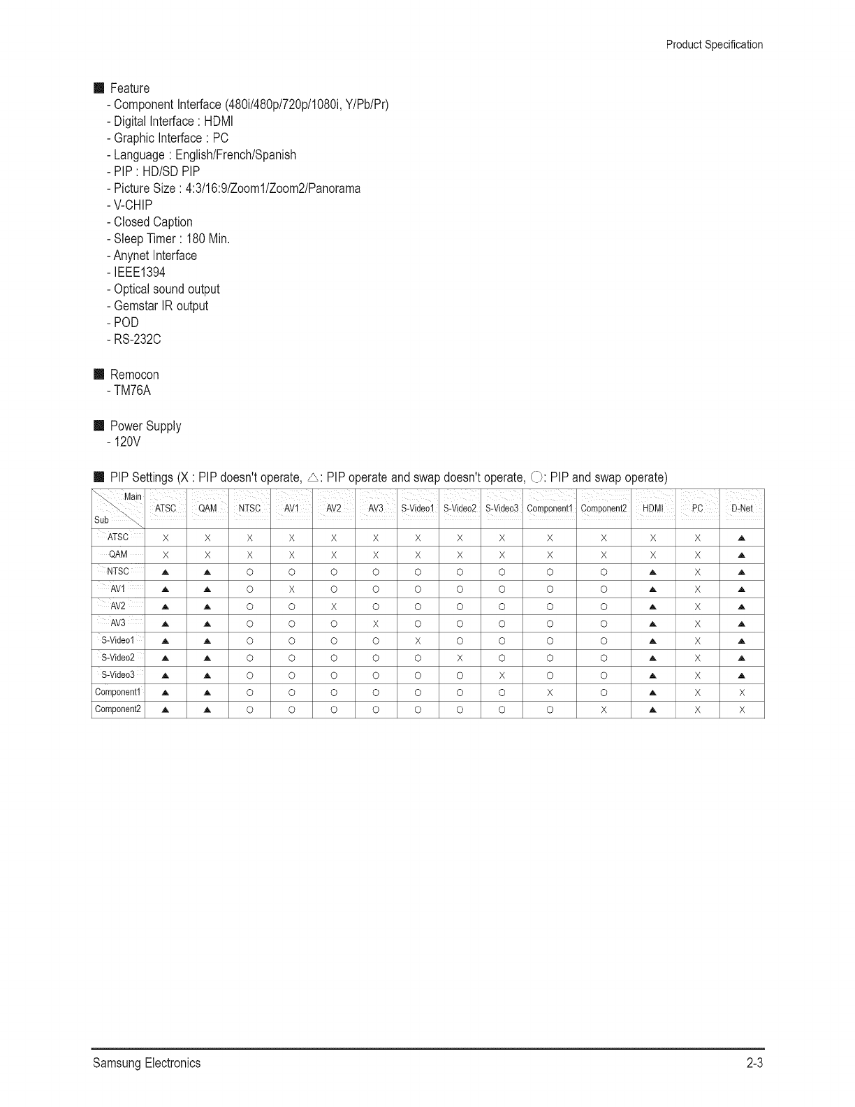
II Feature
- ComponentInterface(480i/480p/720p/1080i,Y/Pb/Pr)
- DigitalInterface: HDMI
- GraphicInterface: PC
- Language: English/French/Spanish
- PiP: HD/SDPiP
- PictureSize : 4:3/16:9/Zoom1/Zoom2/Panorama
- V-CHIP
- ClosedCaption
- SleepTimer: 180Min,
- AnynetInterface
-IEEE1394
- Opticalsoundoutput
- GemstarIRoutput
- POD
- RS-232C
m Remocon
- TM76A
II PowerSupply
- 120V
II PIPSettings(X : PIPdoesn'toperate,_: PIPoperateandswapdoesn'toperate,__: PIPandswapoperate)
ATSC X X X X X X X X X X X X X ,_
QAM X X X X X X X X X X X X X ,_
NTSC A A OOOOOOO O O A X,_
A A O X O O O O O O O A X A
AV2 A A O O X O O O O O O A X A
AV3 ,_. ,_. OOOXOOO O O ,_ X,_
S-Video1 A, A, O O O O X O O O O ,_ X,_
S-Video2 A, A, O O O O O X O O O A X ,_
S-Video3 ,_. ,_. OOOOOO X O O ,_ X,_
Component1 A, A, O O O O O O O X O ,_ X X
Component2 ,_. ,_. OOOOOOO O X ,_ X X
SamsungElectronics 2-3

Product Specification
2-3 Specifications Analysis
Model HL-R5078W HL-R5668W HL-R6168W HL-R6768W HL-R5087W HL-R5688W
N!
Design
DisplayDevice DLP DLP DLP DLP DLP DLP
Built-tnTuner ATSC, NTSC ATSC, NTSC ATSC,NTSC ATSC,NTSC ATSC,NTSC ATSC,NTSC
1080i,720p, 480p, 1080i,720p, 480p, 1080i,720p, 480p, 1080i,720p, 480p, 1080i,720p, 480p, 1080p,1080i,720p,
DisplayFormat 480i 480i 480i 480i 480i 480p,480i
Screen Size 50 inch 56 inch 61 inch 67 inch 50 inch 56 inch
Aspect ratio 16:9 16:9 16:9 16:9 16:9 16:9
Progressivescan Yes Yes Yes Yes Yes Yes
Digital Comb Filter 3D Comb 3D Comb 3D Comb 3D Comb 3D Comb 3D Comb
Picture FirstSurface Mirror Yes Yes Yes Yes Yes Yes
Brightness 800cd/T; 600cd/r; 500cd/,: 500cd/, 800cd/r; 800cd/T;
Contrast 10000:1 10000:1 10000:1 10000:1 2500:1 10000:1
ColorWheel Size/Bearing 7segment/65¢, 7segment/65¢, 7segment/65¢, 7segment/65¢, 7segment/65¢, 7segment/65¢,
Air Bearing Air Bearing Air Bearing Air Bearing Air Bearing Air Bearing
Anti-glare Sun Screen Yes Yes Yes Yes Yes Yes
Screen Pitch 0.098mm 0.098mm 0.098mm 0.098mm 0.098mm 0.098mm
Image enhancer DNle4 DNle4 DNle4 DNle4 DNle3 DNle4
DMD xHD3 xHD3 xHD3 xHD3 xHD2 xHD3
Base/Tremble/Balance No No No No No No
Equalizer 5 Band 5Band 5 Band 5 Band 5 Band 5 Band
Auto VolumeLeveler Yes Yes Yes Yes Yes Yes
Audio TruSurroundXT TruSurroundXT TruSurroundXT TruSurroundXT TruSurroundXT TruSurroundXT
SurroundSound Dolby Digital DolbyDigital DolbyDigital DolbyDigital DolbyDigital DolbyDigital
Speakersystem 2 Way 4 Speaker 2 Way 4 Speaker 2 Way4 Speaker 2Way 4 Speaker 2 Way4 Speaker 2 Way4 Speaker
Output Power 15Wx2 15Wx2 15Wx2 15Wx2 15Wx2 15Wx2
2-Tuner Split-ScreenPIP Yes(HD/SD/QAM) Yes(HD/SD/QAM Yes(HD/SD/QAM) Yes(HD/SD/QAM) Yes(HD/SD) Yes(HD/SD/QAM)
Split-screen Side-by-Side Yes Yes Yes Yes Yes Yes
Features MTS with dbx Noise Yes Yes Yes Yes Yes Yes
Reduction/SAP
Still Picture Yes Yes Yes Yes Yes Yes
Plug & Play Yes Yes Yes Yes Yes Yes
EPG Gemstar EPG Gemstar EPG Gemstar EPG Gemstar EPG Gemstar EPG Gemstar EPG
Yes Yes Yes Yes Yes Yes
S-VideoIn Rear 2/Side 1 Rear 2/Side 1 Rear 2/Side 1 Rear 2/Side 1 Rear 2 Rear 2
Connections HDTV Component
Video Input (Y, Pb, Pr) Rear 2 Rear 2 Rear 2 Rear 2 Rear 2 Rear 2
1080i/480P/480i
PC Yes Yes Yes Yes No No
HDM] Yes Yes Yes Yes Yes Yes
DigitalSound Optical 1 Optical 1 Optical 1 Optical 1 Optical 1 Optical1
2-4 SamsungElectronics
Product Specification
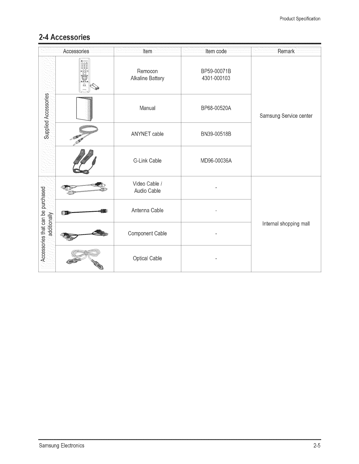
2-4Accessories
Accessories
oa
_ooOi
?
i ¸
iii _ i
il i
i ii
Item I ttem€ode IRemark
Remocon
AlkalineBattery
Manuai
ANYNETcable
G-LinkCable
VideoCable/
AudioCable
AntennaCable
ComponentCable
OpticalCable
BP59-00071B
4301-000103
BP68-00520A
BN39-00518B
MD96-00036A
SamsungServicecenter
Internalshoppingmall
SamsungElectronics 2-5

Alignment & Adjustment
3. Alignment&Adjustment
3-1 Service Instruction
Checkitemslistedafterchangingeach
_::- _. Check !terns L;Actuator
....::: _/vv versionI PromLUU imaex uelay I ^ '
Rep aced terns £5.aln
V-Positi0n'
H-Position CCA Board T'!tFOCUS
Digital Board • • • • •
Analog Board • •
PowerBoard • • •
optical Engine • • • • • •
DMD Board • •
Lamp •
Color Wheel • •
Front LEDAssy •
Actuator
SubdetectorBoard •
1. Softwareversioncheck:
After Enteringthe Servicemode,Checkthe list below
* S/W Notation
"T_EXCAAUSO_00XX"indicates"EXCALIBURBASICMODELUSA,ver.0001".
2. FrontInformationWindowcheck : Seepage6-7.
3. IndexDelayadjustment: Seepage3-15.
4. ActuatorGainadjustment:Seepage3-17.
5. Vertical/HorizontalPositionadjustment: Seepage3-15.
6. CCA: Seepage3-16.
7. BoardLEDcheck : Checkallthe LEDareturnedon.
(in the Analog,DetectBoard)
8. Tilt/Focusadjustment Seepage3-19.
5VA 5,7VB
R7 .R6
3
1.2Kohm
1K
J 1/10W
0P1 0P2
b
PowerCheckIndicatorLED
(AnalogBoard)
12VB
T_EXCAAUSO_00XX
2005 XX XX
T-DTVUCOM5-00XX
T-XMENAUS0_00XX
R8
2K
0Ps
5VA 12VB
P1 (i I
PowerCheckIndicatorLED
(DetectBoard)
SamsungElectronics 3-1
Alignment & Adjustment
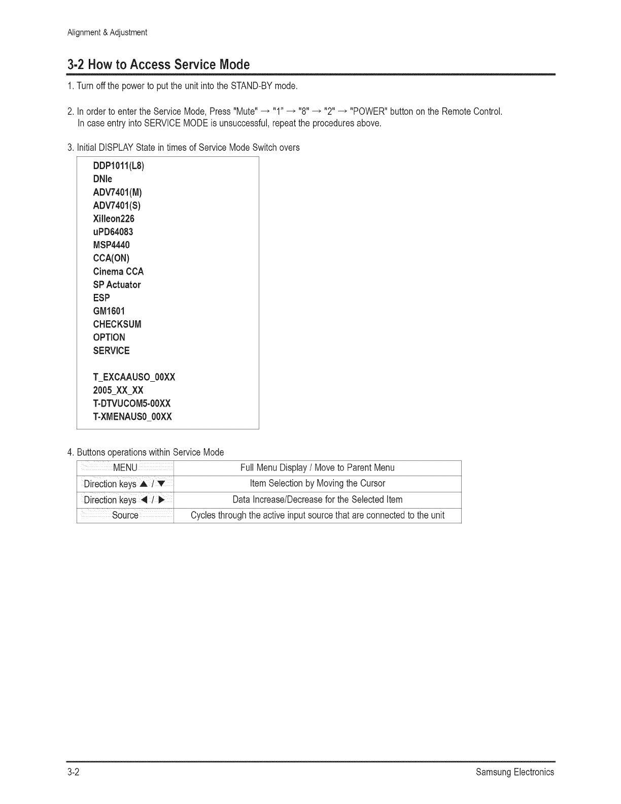
3-2 Howto Access ServiceMode
1,Turnoff the powerto put the unit intothe STAND-BYmode,
2, In orderto enterthe ServiceMode,Press"Mute"--> "1" _ "8" _ "2" _ "POWER"buttonon the RemoteControl,
Incaseentryinto SERVICEMODEis unsuccessful,repeatthe proceduresabove,
3, InitialDISPLAYStatein timesof ServiceModeSwitchovers
DDPlOll(LS)
DNle
ADV7401(M)
ADV7401(S)
Xilleon226
uPD64083
MSP4440
CCA(ON)
CinemaCCA
SPActuator
ESP
GM1601
CHECKSUM
OPTION
SERVICE
T_EXCAAUSO_00XX
2005 XX XX
T-DTVUCOM5-00XX
T-XMENAUS0_00XX
4, ButtonsoperationswithinServiceMode
MENU Full MenuDisplay/Moveto ParentMenu
Directionkeys v ItemSelectionby Movingthe Cursor
Directionkeys 41 DataIncrease/Decreasefor the SelectedItem
source Cyclesthroughthe activeinputsourcethatareconnectedto the unit
3-2 SamsungElectronics
Alignment & Adjustment
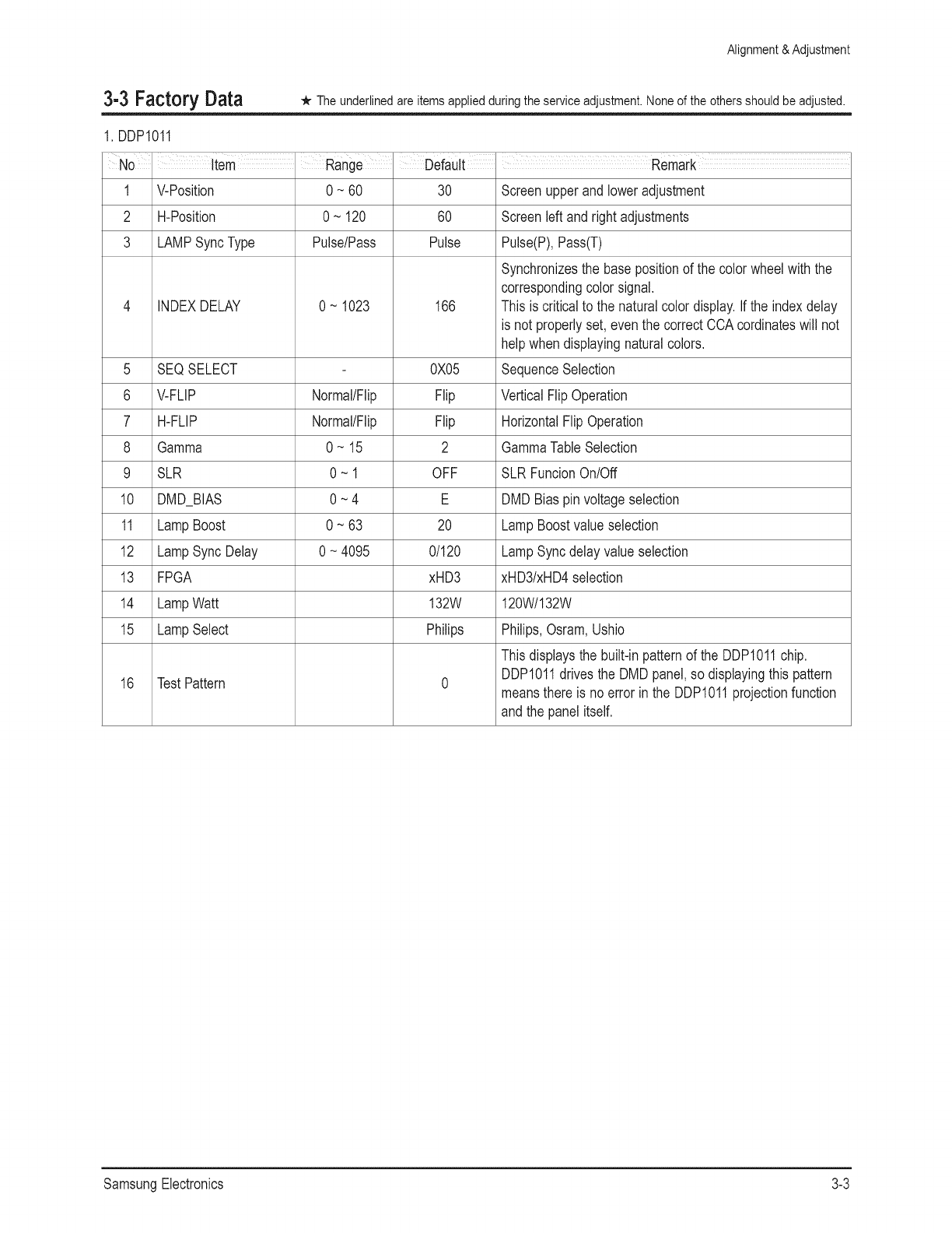
3-3 Factory Data . The underlined are items applied during the service adjustment. None of the others should be adjusted.
1. DDP1011
1 V-Position 0 ~ 60 30
2 H-Position 0 ~ 120 60
3 LAMPSyncType Pulse/Pass Pulse
INDEXDELAY 0 ~ 1023 166
5 SEQSELECT 0X05
6 V-FLIP Normal/Flip Flip
7 H-FLIP Normal/Flip Flip
8 Gamma 0 ~ 15 2
9 SLR 0 ~ 1 OFF
10 DMD_BIAS 0 ~4 E
11 LampBoost 0 ~ 63 20
12 LampSyncDelay 0 ~ 4095 0/120
13 FPGA xHD3
14 LampWatt 132W
15 LampSelect Phiiips
16 TestPattern 0
Screenupperandloweradjustment
Screenleft andrightadjustments
Pulse(P),Pass(T)
Synchronizesthe basepositionof the colorwheelwith the
correspondingcolorsignal.
Thisis criticalto the naturalcolordisplay.If the indexdelay
is not properlyset, eventhe correctCCAcordinateswill not
helpwhen displayingnaturalcolors.
SequenceSelection
VerticalFlipOperation
HorizontalFlip Operation
GammaTableSelection
SLR FuncionOn/Off
DMDBiaspin voltageselection
LampBoostvalueselection
LampSyncdelay valueselection
xHD3/xHD4selection
120W/132W
Philips,Osram,Ushio
Thisdisplaysthe built-inpatternof the DDP1011chip.
DDP1011drivesthe DMDpanel,so displayingthis pattern
meansthereis noerrorin the DDP1011projectionfunction
andthe panelitself.
SamsungElectronics 3-3
Alignment & Adjustment
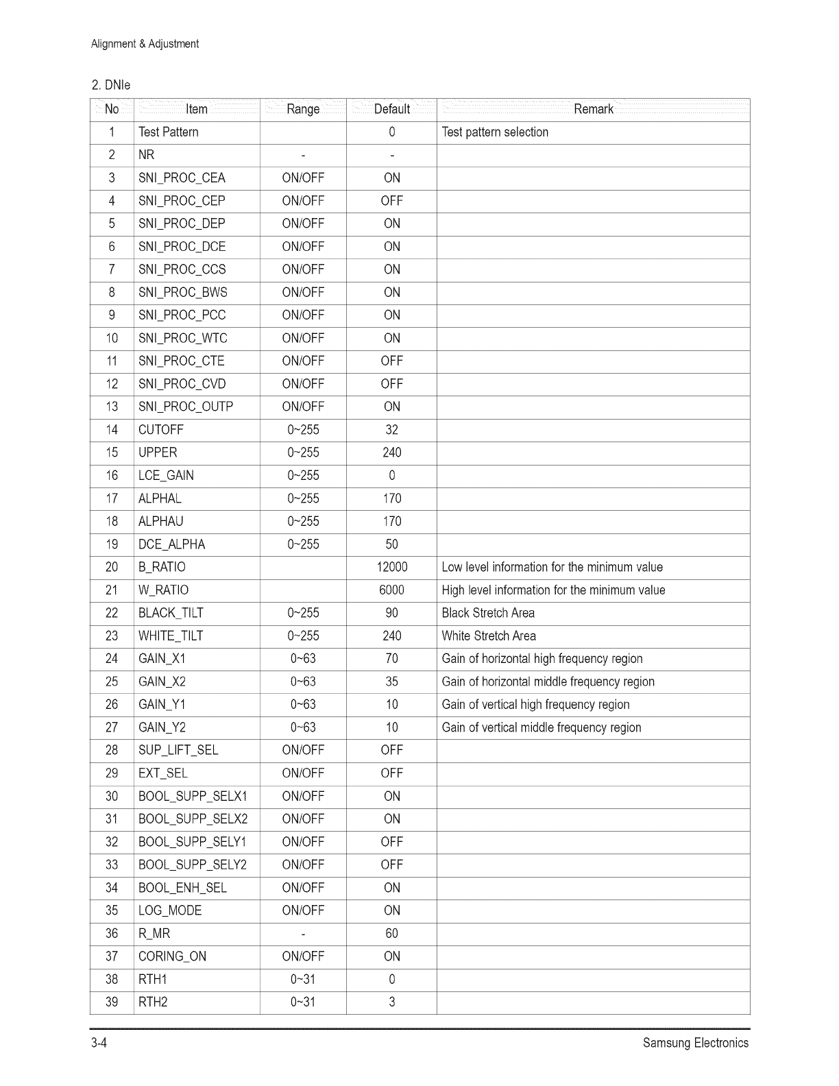
2. DNle
1 TestPattern 0 Testpatternselection
2 NR
3 SNI_PROC_CEA ON/OFF ON
4 SNI_PROC_CEP ON/OFF OFF
5 SNI_PROC_DEP ON/OFF ON
6 SNI_PROC_DCE ON/OFF ON
7 SNI_PROC_CCS ON/OFF ON
8 SNI_PROC_BWS ON/OFF ON
9 SNI_PROC_PCC ON/OFF ON
10 SNI_PROC_WTC ON/OFF ON
11 SNI_PROC_CTE ON/OFF OFF
12 SNI_PROC_CVD ON/OFF OFF
13 SNI_PROC_OUTP ON/OFF ON
14 CUTOFF 0~255 32
15 UPPER 0~255 240
16 LCE_GAIN 0~255 0
17 ALPHAL 0~255 170
18 ALPHAU 0~255 170
19 DCE_ALPHA 0~255 50
20 B_RATIO 12000 Lowlevel informationfor the minimumvalue
21 W_RATIO 6000 Highlevelinformationfor the minimumvalue
22 BLACK_TILT 0~255 90 BlackStretchArea
23 WHITE_TILT 0~255 240 WhiteStretchArea
24 GAIN_X1 0~63 70 Gainof horizontalhighfrequencyregion
25 GAIN_X2 0~63 35 Gainof horizontalmiddlefrequencyregion
26 GAIN_Y1 0~63 10 Gainof verticalhighfrequencyregion
27 GAIN_Y2 0~63 10 Gainof verticalmiddlefrequencyregion
28 SUP_LIFT_SEL ON/OFF OFF
29 EXT_SEL ON/OFF OFF
30 BOOL_SUPP_SELXl ON/OFF ON
31 BOOL_SUPP_SELX2 ON/OFF ON
32 BOOL_SUPP_SELY1 ON/OFF OFF
33 BOOL_SUPP_SELY2 ON/OFF OFF
34 BOOL_ENH_SEL ON/OFF ON
35 LOG_MODE ON/OFF ON
36 R_MR 60
37 CORING_ON ON/OFF ON
38 RTHI 0~31 0
39 RTH2 0~31 3
3-4 SamsungElectronics
Alignment & Adjustment
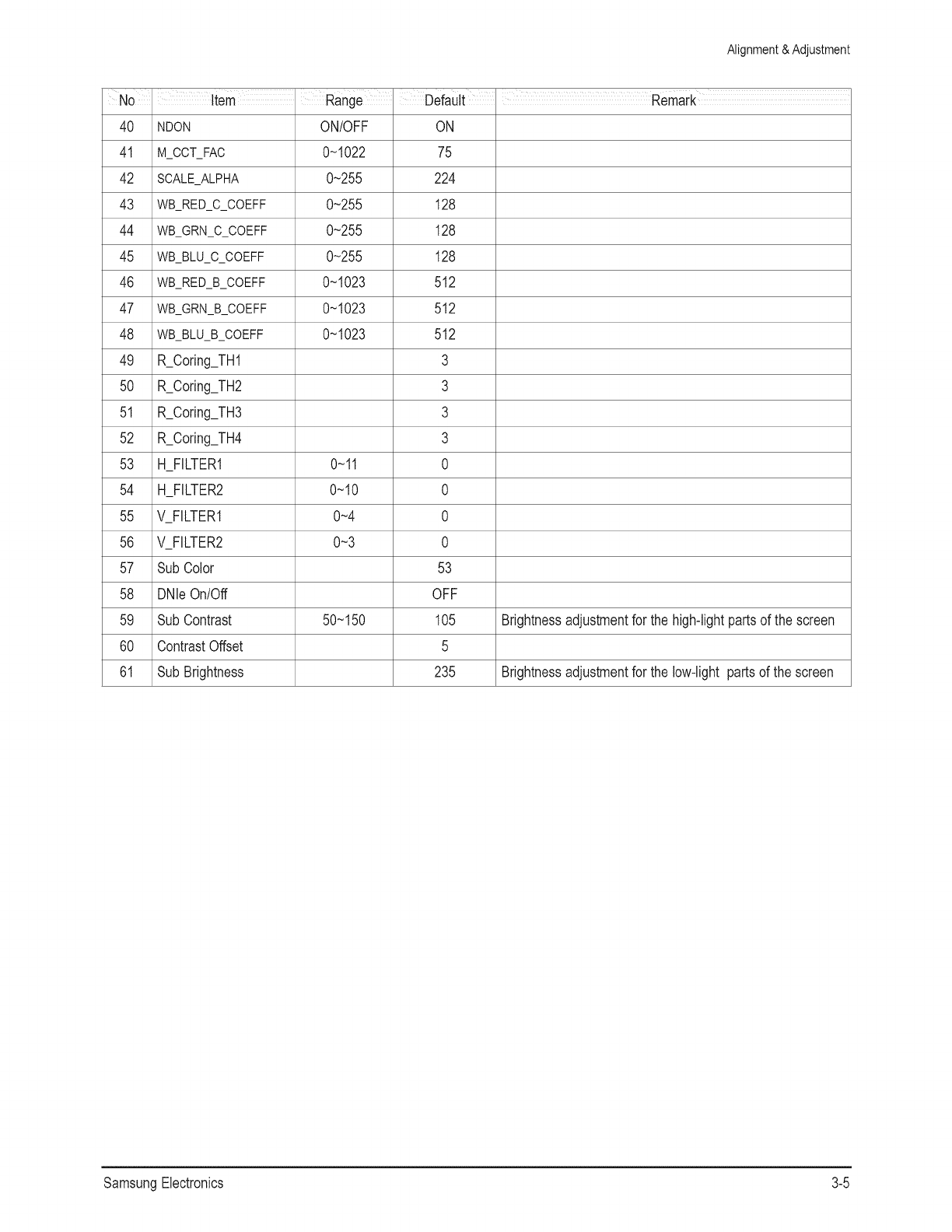
4O
41
42
43
44
45
46
47
48
49
5O
51
52
53
54
55
56
57
58
59
60
61
NDON
M_CCT_FAC
SCALE_ALPHA
WB RED C COEFF
WB_GRN C COEFF
WB BLU C COEFF
WB RED B COEFF
WB_GRN B COEFF
WB BLU B COEFF
R_Coring_TH1
R_Coring_TH2
R_Coring_TH3
R_Coring_TH4
ON/OFF
0~1022
0~255
0~255
0~255
0~255
0~1023
0~1023
0~1023
ON
75
224
128
128
128
512
512
512
3
3
3
3
H_FILTER1 0~11 0
H_FILTER2 0~10 0
V_FILTERI 0~4 0
V_FILTER2 0~3 0
SubColor 53
DNleOn/Off OFF
SubContrast 50~150 105 Brightnessadjustmentfor the high-lightpartsof the screen
ContrastOffset 5
SubBrightness 235 Brightnessadjustmentfor the low-light partsof thescreen
SamsungElectronics 3-5
Alignment & Adjustment
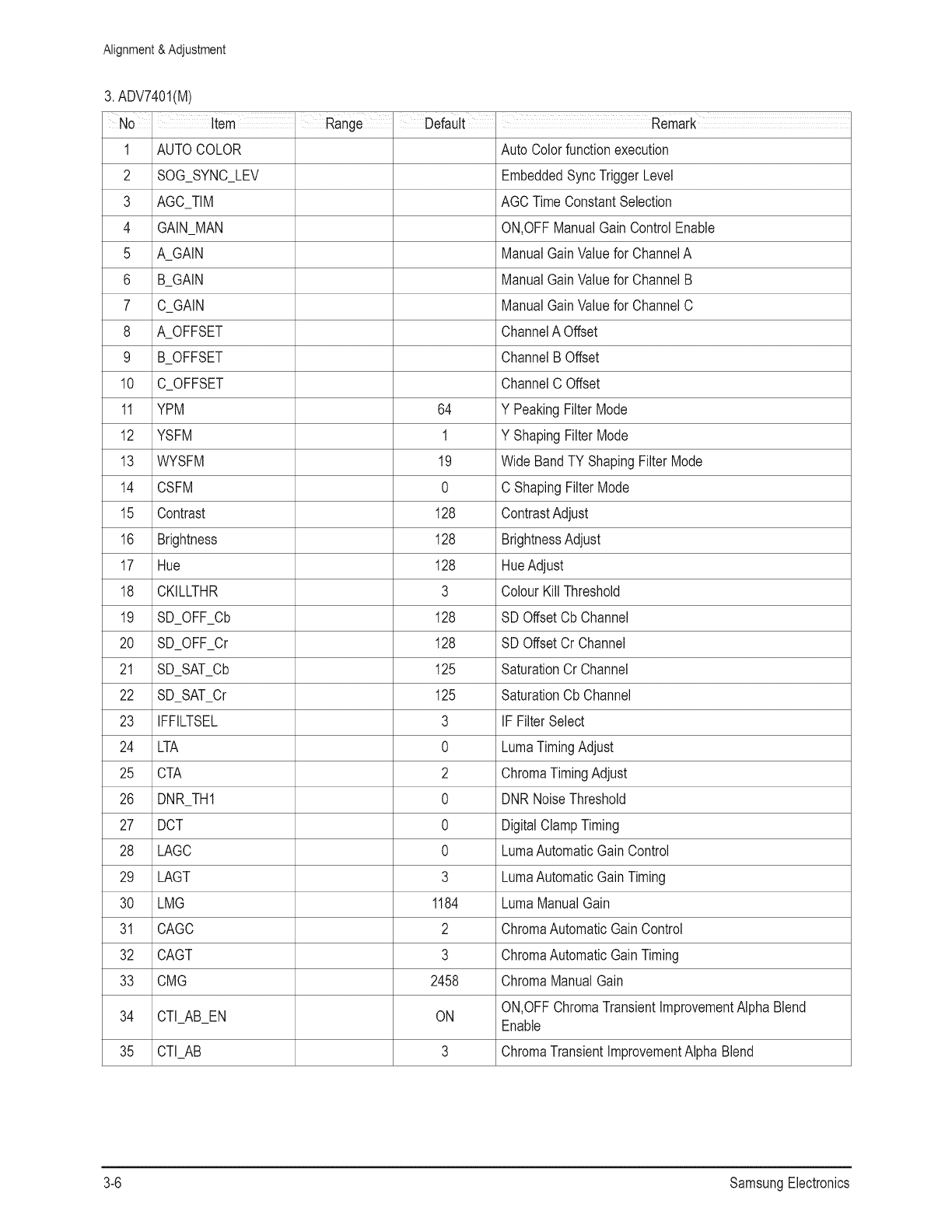
3.ADV7401(M)
1 AUTOCOLOR
2 SOG_SYNC_LEV
3 AGC_TIM
4 GAIN_MAN
5 A_GAIN
6 B_GAIN
7 C_GAIN
8 A_OFFSET
9 B_OFFSET
10 C_OFFSET
11 YPM 64
12 YSFM 1
13 WYSFM 19
14 CSFM 0
15 Contrast 128
16 Brightness 128
17 Hue 128
18 CKILLTHR 3
19 SD_OFF_Cb 128
20 SD_OFF_Cr 128
21 SD_SAT_Cb 125
22 SD_SAT_Cr 125
23 IFFILTSEL 3
24 LTA 0
25 CTA 2
26 DNR_THI 0
27 DCT 0
28 LAGC 0
29 LAGT 3
30 LMG 1184
31 CAGC 2
32 CAGT 3
33 CMG 2458
34 CTI AB EN ON
35 CTI_AB 3
Auto Colorfunctionexecution
EmbeddedSyncTriggerLevel
AGC TimeConstantSelection
ON,OFFManualGainControlEnable
ManualGainValuefor ChannelA
ManualGainValuefor ChannelB
ManualGainValuefor ChannelC
ChannelA Offset
ChannelB Offset
ChannelC Offset
Y PeakingFilterMode
Y ShapingFilterMode
WideBandTY ShapingFilterMode
C ShapingFilterMode
ContrastAdjust
BrightnessAdjust
HueAdjust
ColourKillThreshold
SD OffsetCb Channel
SD OffsetCr Channel
SaturationCr Channel
SaturationCb Channel
IF FilterSelect
LumaTimingAdjust
ChromaTimingAdjust
DNRNoiseThreshold
DigitalClampTiming
LumaAutomaticGainControl
LumaAutomaticGainTiming
LumaManualGain
ChromaAutomaticGainControl
ChromaAutomaticGainTiming
ChromaManualGain
ON,OFFChromaTransientImprovementAlphaBlend
Enable
ChromaTransientImprovementAlphaBlend
3-6 SamsungElectronics
Alignment & Adjustment
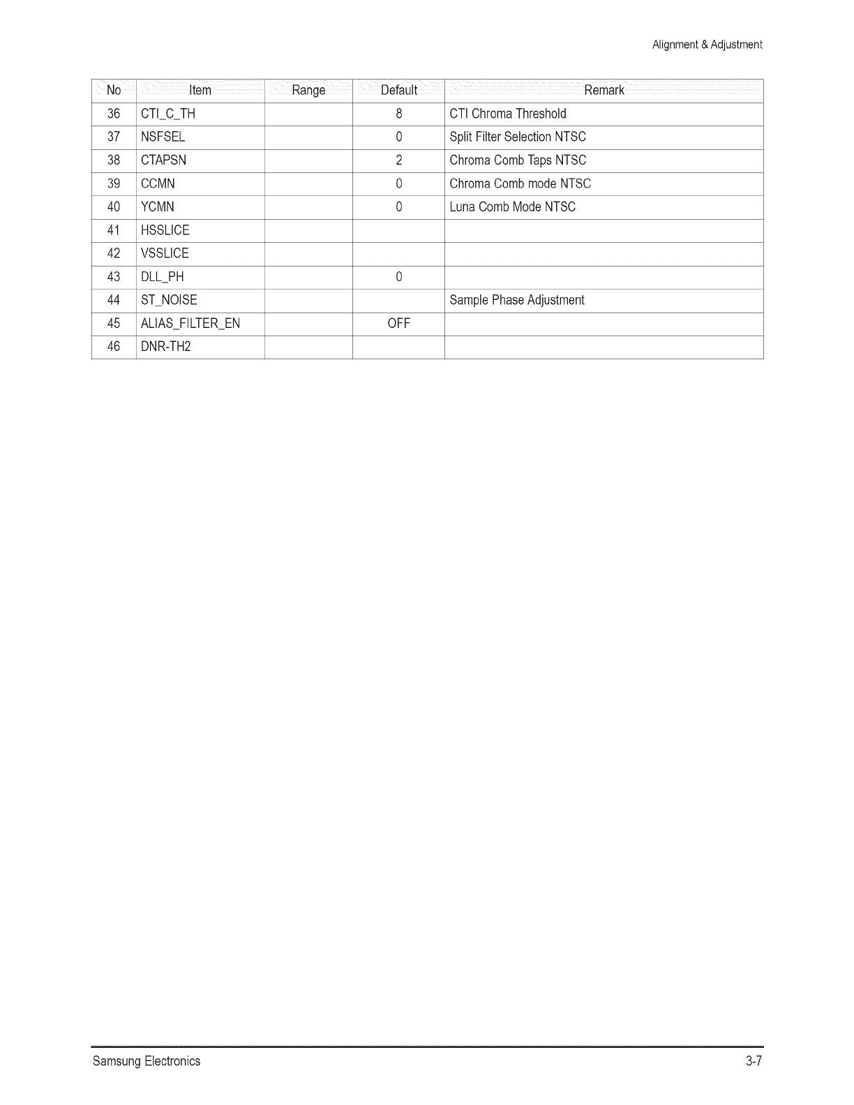
36 CTI C TH
37 NSFSEL
38 CTAPSN
39 CCMN
40 YCMN
41 HSSLICE
42 VSSLICE
43 DLL_PH
44 ST_NOISE
45 ALIAS_FILTER_EN
46 DNR-TH2
8
0
2
0
0
CTI ChromaThreshold
Split FilterSelectionNTSC
ChromaCombTapsNTSC
ChromaCombmodeNTSC
LunaCombModeNTSC
0
SamplePhaseAdjustment
OFF
SamsungElectronics 3-7
Alignment & Adjustment
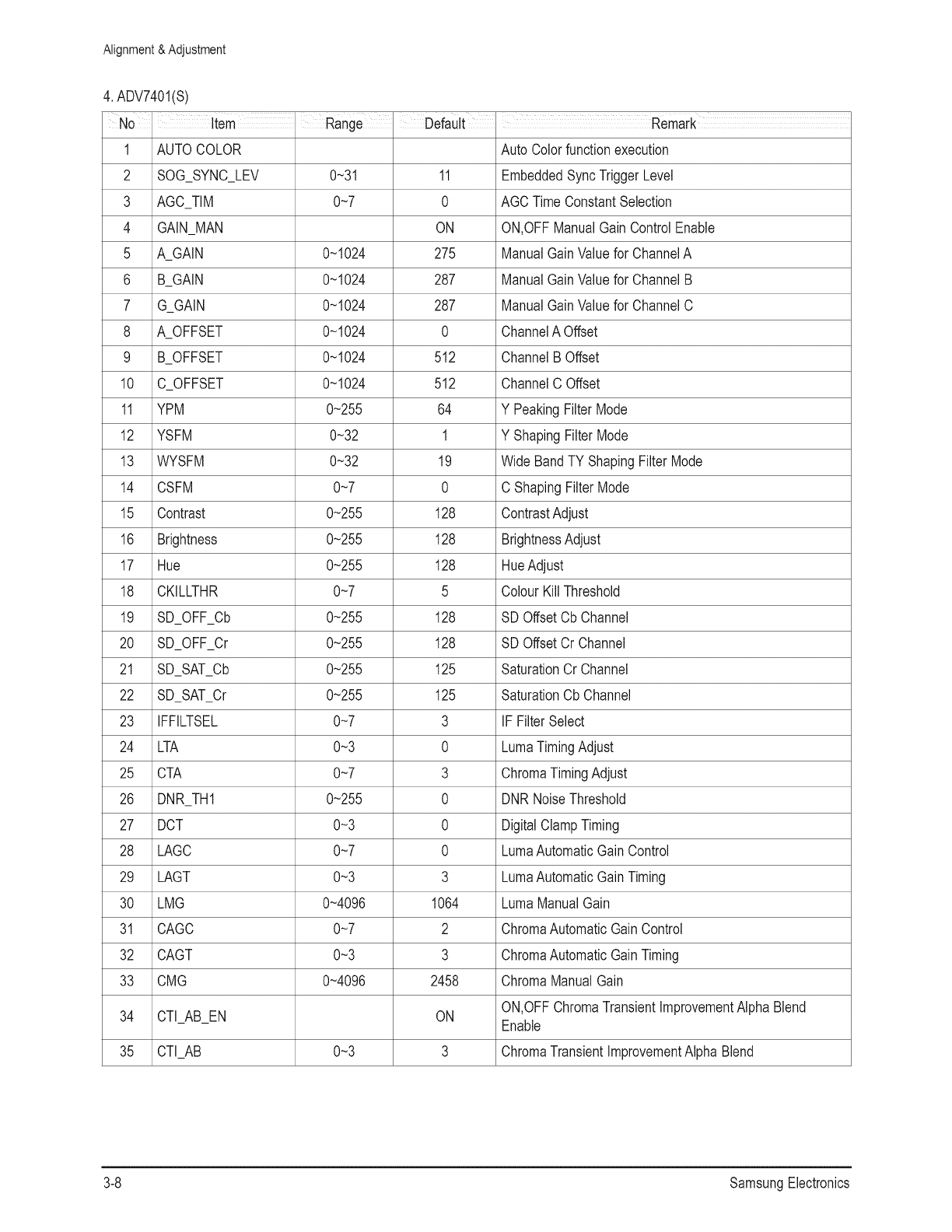
4. ADV7401(S)
1 AUTOCOLOR
2 SOG_SYNC_LEV 0~31 11
3 AGC_TIM 0~7 0
4 GAIN_MAN ON
5 A_GAIN 0~1024 275
6 B_GAIN 0~1024 287
7 G_GAIN 0~1024 287
8 A_OFFSET 0~1024 0
9 B_OFFSET 0~1024 512
10 C_OFFSET 0~1024 512
11 YPM 0~255 64
12 YSFM 0~32 1
13 WYSFM 0~32 19
14 CSFM 0~7 0
15 Contrast 0~255 128
16 Brightness 0~255 128
17 Hue 0~255 128
18 CKILLTHR 0~7 5
19 SD_OFF_Cb 0~255 128
20 SD_OFF_Cr 0~255 128
21 SD_SAT_Cb 0~255 125
22 SD_SAT_Cr 0~255 125
23 IFFILTSEL 0~7 3
24 LTA 0~3 0
25 CTA 0~7 3
26 DNR_THI 0~255 0
27 DCT 0~3 0
28 LAGC 0~7 0
29 LAGT 0~3 3
30 LMG 0~4096 1064
31 CAGC 0~7 2
32 CAGT 0~3 3
33 CMG 0~4096 2458
34 CTI AB EN ON
35 CTI_AB 0~3 3
Auto Colorfunctionexecution
EmbeddedSyncTriggerLevel
AGC TimeConstantSelection
ON,OFFManualGainControlEnable
ManualGainValuefor ChannelA
ManualGainValuefor ChannelB
ManualGainValuefor ChannelC
ChannelA Offset
ChannelB Offset
ChannelC Offset
Y PeakingFilterMode
Y ShapingFilterMode
WideBandTY ShapingFilterMode
C ShapingFilterMode
ContrastAdjust
BrightnessAdjust
HueAdjust
ColourKillThreshold
SD OffsetCb Channel
SD OffsetCr Channel
SaturationCr Channel
SaturationCb Channel
IF FilterSelect
LumaTimingAdjust
ChromaTimingAdjust
DNRNoiseThreshold
DigitalClampTiming
LumaAutomaticGainControl
LumaAutomaticGainTiming
LumaManualGain
ChromaAutomaticGainControl
ChromaAutomaticGainTiming
ChromaManualGain
ON,OFFChromaTransientImprovementAlphaBlend
Enable
ChromaTransientImprovementAlphaBlend
3-8 SamsungElectronics
Alignment & Adjustment
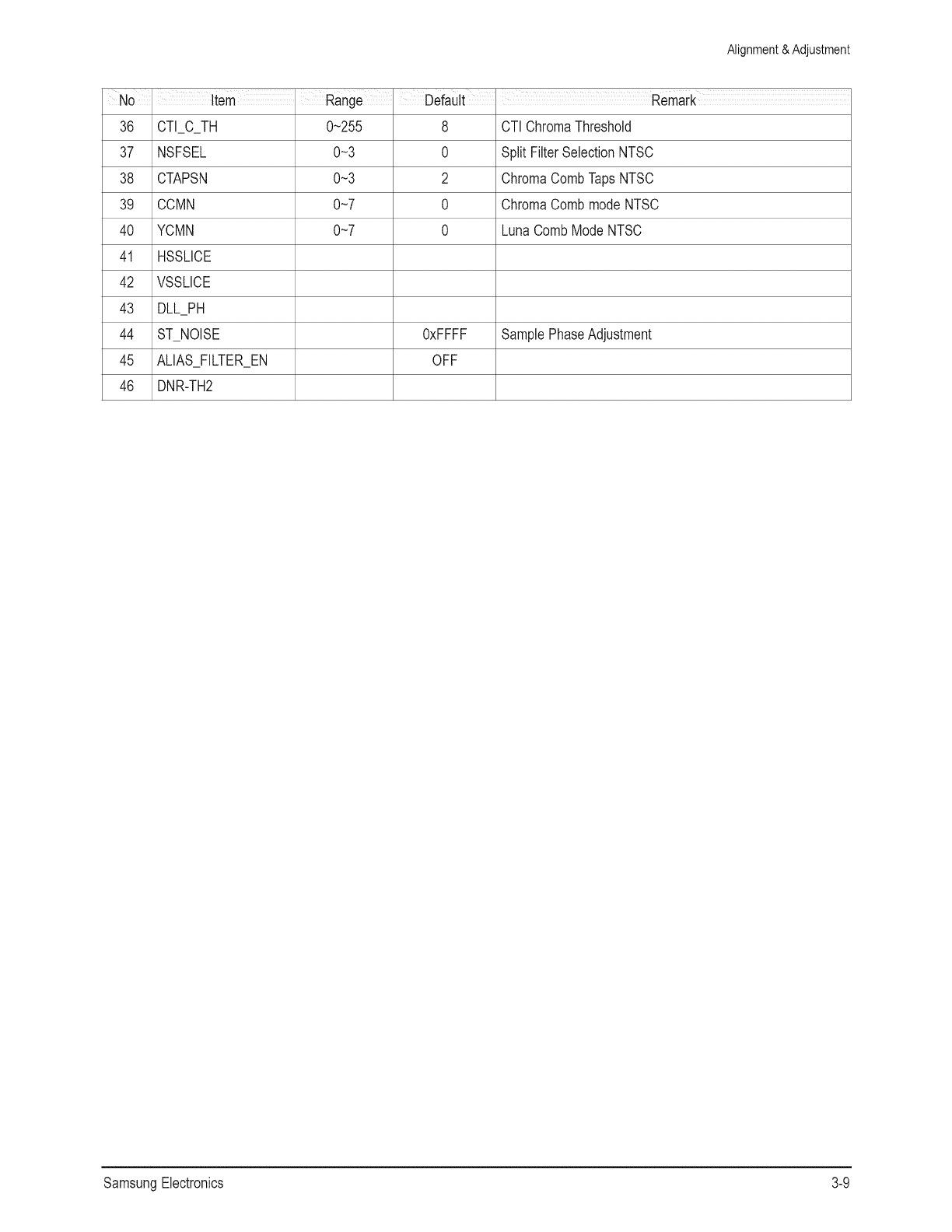
36 CTI C TH
37 NSFSEL
38 CTAPSN
39 CCMN
40 YCMN
41 HSSLICE
42 VSSLICE
43 DLL_PH
44 ST_NOISE
45 ALIAS_FILTER_EN
46 DNR-TH2
0~255
0~3
0~3
0~7
0~7
8
0
2
0
0
CTI ChromaThreshold
Split FilterSelectionNTSC
ChromaCombTapsNTSC
ChromaCombmodeNTSC
LunaCombModeNTSC
0xFFFF SamplePhaseAdjustment
OFF
SamsungElectronics 3-9
Alignment & Adjustment
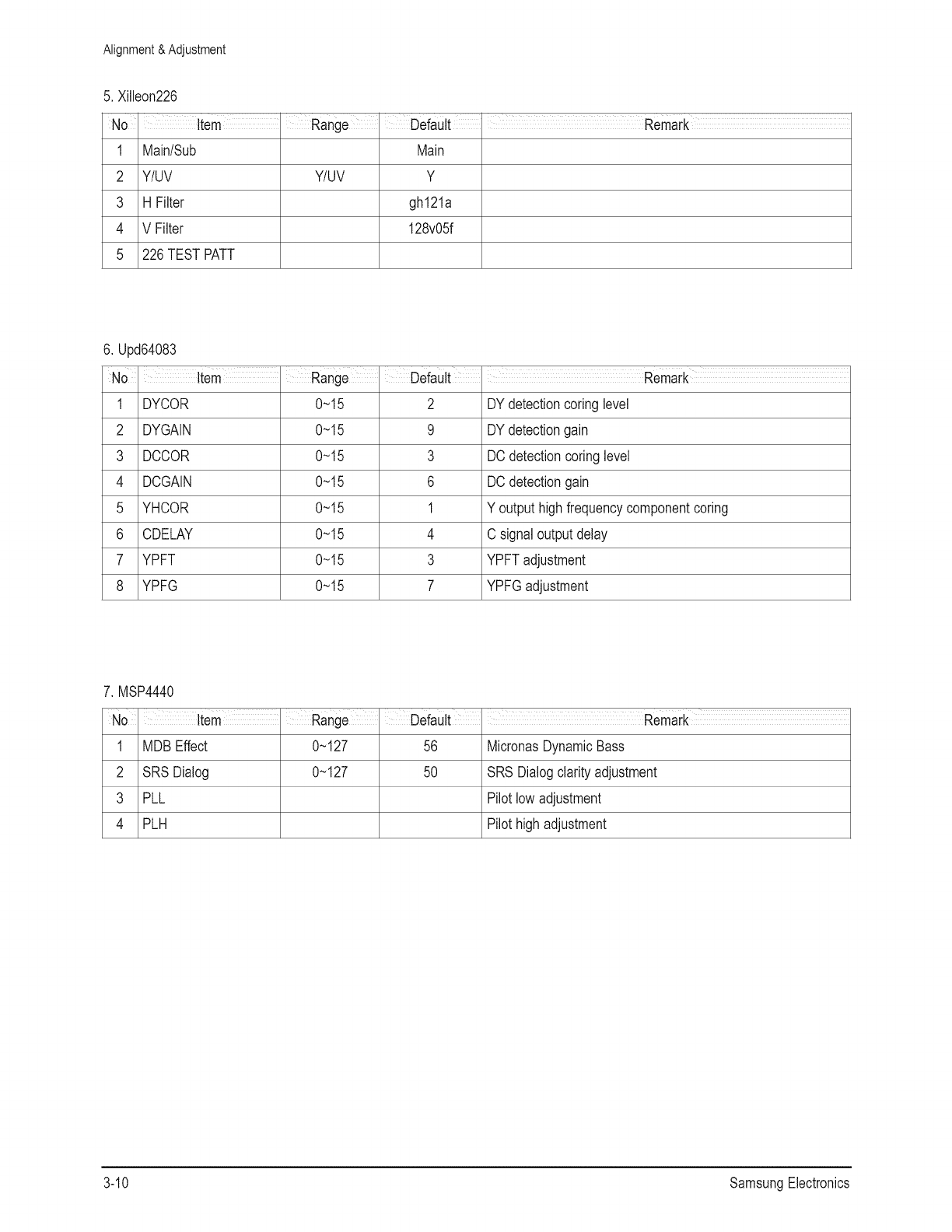
5, Xilieon226
1 Main/Sub Main
2 Y/UV Y/UV Y
3 H Filter gh121a
4 V Filter 128v05f
5 226TESTPATT
6, Upd64083
1 DYCOR 0~15 2 DYdetectioncoringlevel
2 DYGAIN 0~15 9 DYdetectiongain
3 DCCOR 0~15 3 DCdetectioncoringlevel
4 DCGAIN 0~15 6 DCdetectiongain
5 YHCOR 0~15 1 Y outputhighfrequencycomponentcoring
6 CDELAY 0~15 4 C signaloutputdelay
7 YPFT 0~15 3 YPFTadjustment
8 YPFG 0~15 7 YPFGadjustment
7, MSP4440
1 MDBEffect 0~127 56 MicronasDynamicBass
2 SRS Dialog 0~127 50 SRSDialogclarityadjustment
3 PLL Pilotlow adjustment
4 PLH Pilothighadjustment
3-10 SamsungElectronics
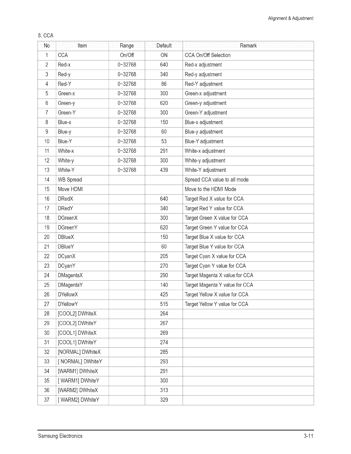
8,CCA
Alignment & Adjustment
1 CCA On/Off ON CCAOn/OffSelection
2 Red-x 0~32768 640 Red-xadjustment
3 Red-y 0~32768 340 Red-yadjustment
4 Red-Y 0~32768 86 Red-Yadjustment
5 Green-x 0~32768 300 Green-xadjustment
6 Green-y 0~32768 620 Green-yadjustment
7 Green-Y 0~32768 300 Green-Yadjustment
8 Blue-x 0~32768 150 Blue-xadjustment
9 Blue-y 0~32768 60 Blue-yadjustment
10 Blue-Y 0~32768 53 Blue-Yadjustment
11 White-x 0~32768 291 White-xadjustment
12 White-y 0~32768 300 White-yadjustment
13 White-Y 0~32768 439 White-Yadjustment
14 WBSpread SpreadCCAvalueto all mode
15 MoveHDMI Moveto the HDMIMode
16 DRedX 640 TargetRed Xvaluefor CCA
17 DRedY 340 TargetRedY valuefor CCA
18 DGreenX 300 TargetGreenX valuefor CCA
19 DGreenY 620 TargetGreenY valuefor CCA
20 DBlueX 150 TargetBlueX valuefor CCA
21 DBlueY 60 TargetBlueYvalue for CCA
22 DCyanX 205 TargetCyanX valuefor CCA
23 DCyanY 270 TargetCyanY valuefor CCA
24 DMagentaX 290 TargetMagentaX valuefor CCA
25 DMagentaY 140 TargetMagentaY valuefor CCA
26 DYellowX 425 TargetYellowX valuefor CCA
27 DYellowY 515 TargetYellowY valuefor CCA
28 [COOL2]DWhiteX 264
29 [COOL2]DWhiteY 267
30 [COOL1]DWhiteX 269
31 [COOL1]DWhiteY 274
32 [NORMAL]DWhiteX 285
33 [ NORMAL]DWhiteY 293
34 [WARM1]DWhiteX 291
35 [ WARM1]DWhiteY 300
36 [WARM2]DWhiteX 313
37 [ WARM2]DWhiteY 329
SamsungElectronics 3-11
Alignment & Adjustment
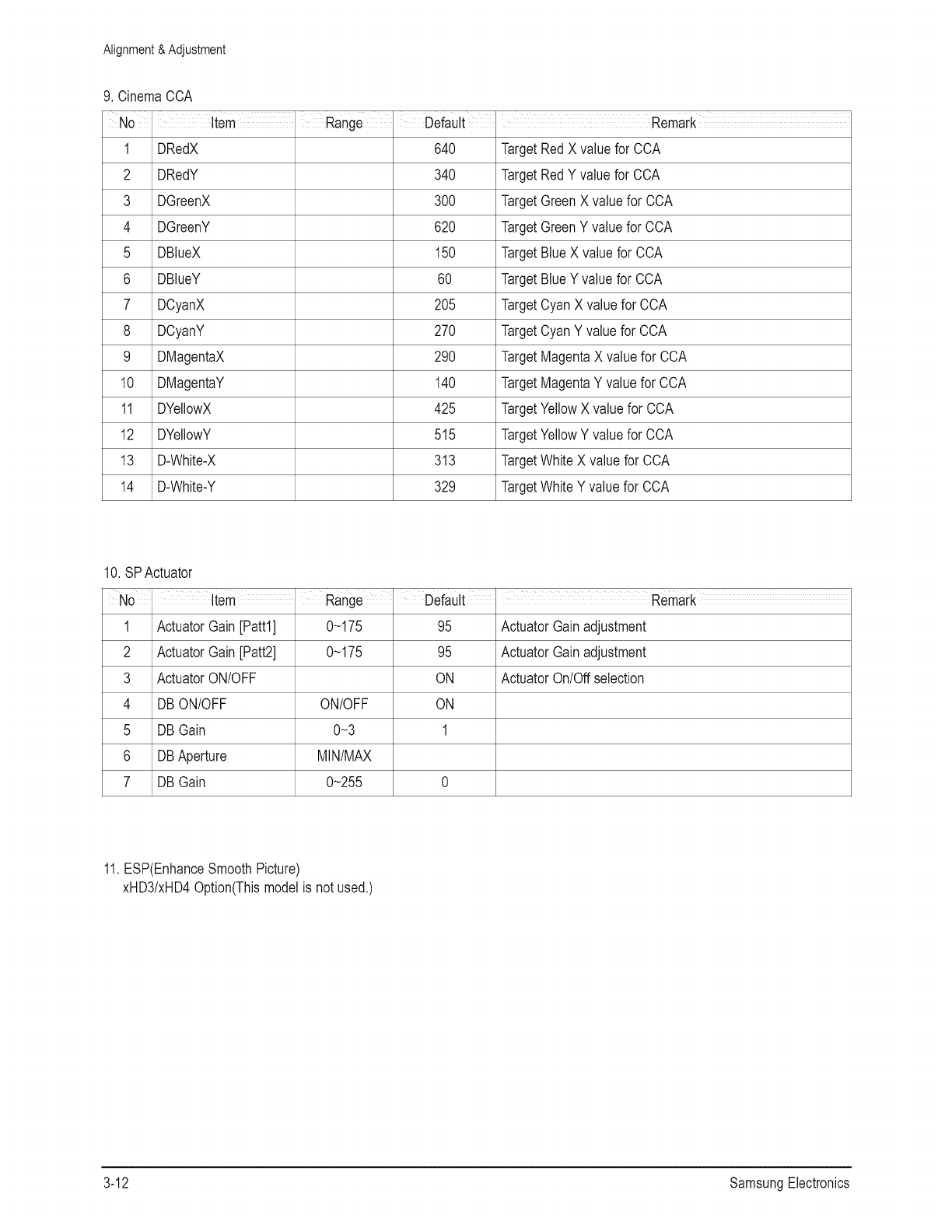
9, CinemaCCA
1 DRedX 640 TargetRed Xvaluefor CCA
2 DRedY 340 TargetRedY valuefor CCA
3 DGreenX 300 TargetGreenX valuefor CCA
4 DGreenY 620 TargetGreenY valuefor CCA
5 DBlueX 150 TargetBlueX valuefor CCA
6 DBlueY 60 TargetBlueYvalue for CCA
7 DCyanX 205 TargetCyanX valuefor CCA
8 DCyanY 270 TargetCyanY valuefor CCA
9 DMagentaX 290 TargetMagentaX valuefor CCA
10 DMagentaY 140 TargetMagentaY valuefor CCA
11 DYellowX 425 TargetYellowX valuefor CCA
12 DYellowY 515 TargetYellowY valuefor CCA
13 D-White-X 313 TargetWhiteX valuefor CCA
14 D-White-Y 329 TargetWhiteY valuefor CCA
10,SPActuator
1 ActuatorGain[Pattl] 0~175 95 ActuatorGainadjustment
2 ActuatorGain[Patt2] 0~175 95 ActuatorGainadjustment
3 ActuatorON/OFF ON ActuatorOn/Offselection
4 DBON/OFF ON/OFF ON
5 DBGain 0~3 1
6 DBAperture MINIMAX
7 DBGain 0~255 0
11,ESP(EnhanceSmoothPicture)
xHD3/xHD4Option(Thismodelis notused,)
3-12 SamsungElectronics

12,GM1601
Alignment & Adjustment
1 ADC_RED_GAIN 128
2 ADC_GRN_GAIN 128
3 ADC_BLU_GAIN 128
4 ADC_RED_OFFSET 50
5 ADC_GRN_OFFSET 50
6 ADC_BLU_OFFSET 50
7 MADI_QUANT_TH0 4
8 MADI_QUANT_THI 7
9 MADI_QUANT_TH2 64
10 GAMMA_CONTROL OFF
11 AUTO_COLOR OFF
12 TEST_PATTERN 0
13 SP_AMP 0
14 SP_PERIOD 0
13,OPTION
1 LampClear Initializelampusagetime, LampLife is set to zero
2 UserReset All user settingsaresetto default
3 WB Reset OFF Initializethe WhiteBalancevalue
4 EERReset Clearthe EEPROM
5 LampLife Lampontimecounter
Thesets turnsonautomaticallywhen the powercord is
6 AUTOPOWER ON pluggedin
7 DNleDemo ON/OFF ON DNIeDemofunctionselection
8 LampControl DynamidNormal Dynamic Dynamic,Always
Timewhichthescreenwill beblackwhileswitching
9 MUTETIME 400ms channels
10 EDIDWRITE
11 DDCProtection ON/OFF OFF DDCwriteON/OFFselection
12 LNADefault Auto!OFF Auto LNAsettingOFF/Autoselection
13 PROTECT ON ProtectionON/OFFselection
14 WATCHDOG OFF WatchDog ON/OFFselection
15 WDCOUNT 0 Countfor WatchDogevent
16 DEBUGMODE ATI226/GM1601 ATI226
17 DSUBMODE RS232
18 BUSSTOP OFF
19 DIGITAL-->DMD Totransthe CCAdataformDIGITALto DMD
20 DMD-->DGITIAL Totransthe CCAdataformDMDto DIGITAL
SamsungElectronics 3-13

Alignment & Adjustment
14,SERVICE
1 V-Position
2 H-Position
3 LAMPSYNC
4 ActuatorGain[_
5 ActuatorGain[_
6 INDEXDELAY
7 FPGA
8 LampWatt
9 LampSelect
10 AUTOCOLOR
11 CCA
12 LampClear
13 UserReset
0 ~ 60
0 ~ 120
0~175
0~175
0 ~ 1023
30
60
95
95
173
xHD3
132W
Phiiips
OFF
Screenupperandloweradjustment
Screenleft andrightadjustments
ActuatorGainadjustment
ActuatorGainadjustment
Indexdelayadjustment
xHD3/xHD4selection
Auto Colorfunctionexecution
CCAmenu
InitializeLampusagetime
All user settingsaresetto default
3-14 SamsungElectronics
Alignment & Adjustment
3-4 ServiceAdjustment
3-4-1 Vertical /Horizontal PositionAdjustment
1.Turnoff the powerto put the unit intothe STAND-BYmode.
2. In orderto enterthe ServiceMode,Press"Mute"_ "1" _ "8" _ "2" _ "POWER"buttonson the RemoteControl.
3. Select"Service"on the first displayof the Servicemodemenu.
4. SelecttheV-positionfor verticalpositioningand H-positionfor horizontalpositioningby usingthe A 'v' (Up& Down)buttons.
Pressthe _ i_ (Leftor Right)buttonsto adjustthe screenposition.
Do notset theV-positionvalueto 34or 35. (Settingto thesevalueswill causehorizontallines onthe right sideof the screen.)
3-4-2 INDEX DELAYAdjustment
1.Turnoff the powerto put the unit intothe STAND-BYmode.
2. In orderto enterthe ServiceMode,Press"Mute"_ "1" _ "8" _ "2" _ "POWER"buttonson the RemoteControl.
3. Select"Service"on the first displayof the Servicemodemenu.
4. Pressthe A v' (Up or Down)buttonto moveto INDEXDELAY,then pressENTERto select.
5. The INDEXDELAYsetupscreen(witha redbarat the bottomof the screen)will be displayed.
6. Pressthe _ _ (Leftof Right)buttonsto adjust.Checkthe redcolor at the bottomof the screenat its minimumandmaximum
valuesof changingfrom redto magenta,thenadjustto the meanvalue.
SamsungElectronics 3-15
Alignment & Adjustment
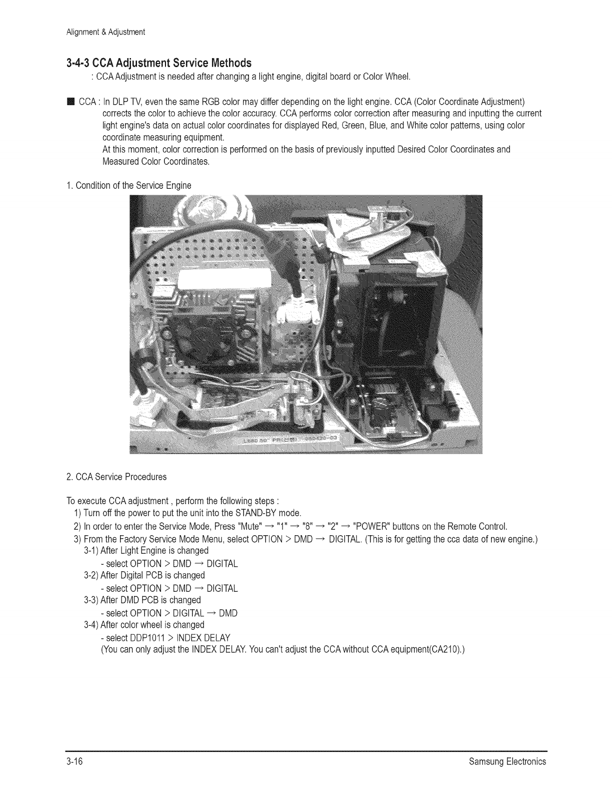
3-4-3 CCA Adjustment Service Methods
: CCAAdjustmentis neededafterchanginga light engine,digital boardor ColorWheel.
II CCA: In DLPTV,eventhe sameRGBcolormaydifferdependingon the light engine.CCA(ColorCoordinateAdjustment)
correctsthe colorto achievethe coloraccuracy.CCAperformscolor correctionaftermeasuringandinputtingthe current
light engine'sdata onactualcolorcoordinatesfor displayedRed,Green,Blue,andWhitecolor patterns,usingcolor
coordinatemeasuringequipment.
At this moment,colorcorrectionis performedon the basisof previouslyinputtedDesiredColorCoordinatesand
MeasuredColorCoordinates.
1. Conditionof the ServiceEngine
2. CCAServiceProcedures
ToexecuteCCAadjustment,performthe followingsteps :
1)Turnoff the powerto put the unit intothe STAND-BYmode.
2) In orderto enterthe ServiceMode,Press"Mute"_ "1"_ "8" _ "2" _ "POWER"buttonson the RemoteControl.
3) Fromthe FactoryServiceModeMenu,selectOPTION> DMD_ DIGITAL.(Thisis for gettingthe ccadataof newengine.)
3-1)AfterLight Engineis changed
- selectOPTION> DMD_ DIGITAL
3-2)AfterDigitalPCBis changed
- selectOPTION> DMD_ DIGITAL
3-3)AfterDMD PCBis changed
- selectOPTION> DIGITAL_ DMD
3-4)Aftercolorwheelis changed
- selectDDP1011> INDEXDELAY
(Youcanonly adjustthe INDEXDELAY.Youcan't adjustthe CCAwithoutCCAequipment(CA210).)
3-16 SamsungElectronics

Alignment & Adjustment
3-4-4 ACTUATOR GAIN Adjustment
1. BeforeAdjustment
1)Turnoff the powerto put the unit intothe STAND-BYmode.
2) In orderto enterthe ServiceMode,Press"Mute"_ "I" _ "8" _ "2" _ "POWER"buttonon theRemoteControl.
3) Select"Service"on thefirst displayof the Servicemodemenu.
4) Pressthe A 'v (Upor Down)buttonto moveto ACTUATORGAIN1,2,then pressENTERto select.
-ActuatorGain1'In caseof controllingwith CrossPattern.
J_
BeforeAdjusting AfterAdjusting
-ActuatorGain2'In caseof controllingwith CrosshatchPattern.
CROSSHATCHPATTERN
.............
.................
÷
.....................bl .....
......._...........+,_,_,,
...............
......4 ........
CAUSTION:GAIN2 isjust controlledbyyour
eye becausecontrol valuedoesn't
appear In picture.
2. MakingAdjustments
1)As shownin the pictureabove,changetheactuatorvaluesto eliminatesaw toothshapes.
- Tofine tune,increasethe data valueensuringthatyou getthe centerbetweenthe startingandendingpointsof the
disappearingsaw toothshape.
SamsungElectronics 3-17

Alignment & Adjustment
3-5 Software Upgrade
1. Preparethe USBmemorystickwiththe built-infirmware.
2. Whilethe TV is off, insertthe USBstickinto the SERVICEterminal.
3. Whenturningonthe TV,thereshouldbea longbeepingtoneand thefirmwaredownloadprocessshouldstart.If thereis no
soundfromthe TV,turn it offandthen on again.
4. Whenthe downloadis complete,therewill beanotherlongbeepingtoneand theTV will go into standbymode.
Checkfor the FirmwareVersion
1)Turnoff the powerto put the unit intothe STAND-BYmode.
2) In orderto enterthe ServiceMode,Press"Mute"--> "1" _ "8" _ "2"_ "POWER"buttonson the RemoteControl.
3) In caseentryinto SERVICEMODEis unsuccessful,repeatsteps 1and2 directlyabove.
4) Youcancheckthe firmwareversionat the bottomof the Factorymenu, T_EXCAAUSO_00XX
2005XX XX
T-DTVUCOM5-00XX
T-XMENAUS0_00XX
3-18 SamsungElectronics
Alignment & Adjustment
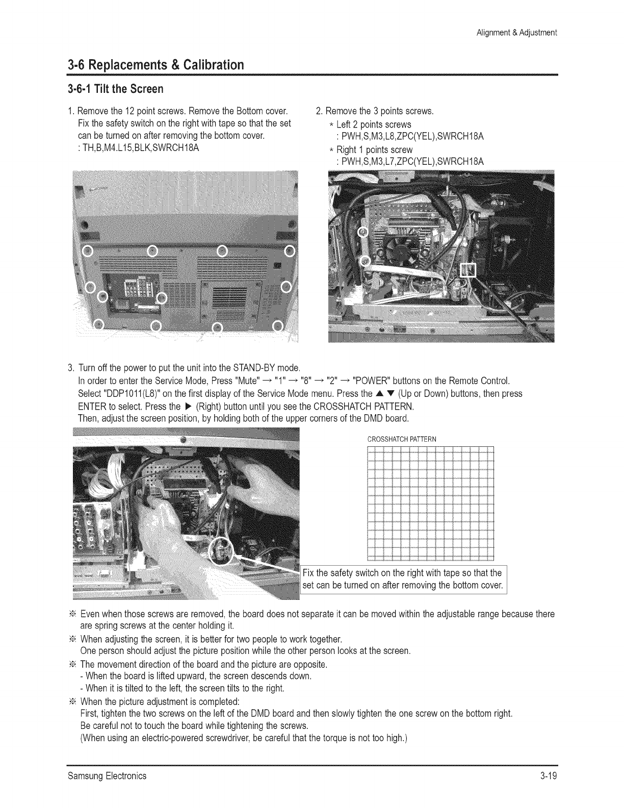
3-6 Replacements & Calibration
3-6-1 Tilt the Screen
1. Removethe 12pointscrews.Removethe Bottomcover.
Fixthesafetyswitchon the rightwithtape so thatthe set
can beturnedon afterremovingthe bottomcover.
: TH,B,M4.L15,BLK,SWRCH18A
2. Removethe 3 pointsscrews.
* Left2 pointsscrews
: PWH,S,M3,L8,ZPC(YEL),SWRCH18A
* Right1 pointsscrew
: PWH,S,M3,L7,ZPC(YEL),SWROH18A
3. Turnoffthe powerto put the unit intothe STAND-BYmode.
Inorderto enter the ServiceMode,Press"Mute"_ "1" _ "8" _ "2" _ "POWER"buttonson the RemoteControl.
Select"DDP1011(L8)"on thefirst displayof the ServiceModemenu.Pressthe A 'v (Upor Down)buttons,then press
ENTERto select.Pressthe !_ (Right)buttonuntil yousee the CROSSHATCHPATTERN.
Then,adjustthe screenposition,by holdingbothof the uppercornersof the DMD board.
CROSSHATCHPATTERN
l
.......#==
Fixthe safetyswitchon the rightwithtape so thatthe ]
set can beturnedonafter removingthe bottomcover.J
-_ Evenwhen thosescrewsare removed,the boarddoesnot separateit can be movedwithinthe adjustablerangebecausethere
are springscrewsat the centerholdingit.
-_ Whenadjustingthe screen,it is betterfor twopeopleto worktogether.
Onepersonshouldadjustthe picturepositionwhile the otherpersonlooksat the screen.
-_ The movementdirectionof the boardandthe pictureare opposite.
- Whenthe boardis liftedupward,the screendescendsdown.
- Whenit is tiltedto the left,the screentilts to the right.
-_ Whenthe pictureadjustmentis completed:
First,tightenthe twoscrewson the leftof the DMDboardandthen slowlytightenthe onescrewonthe bottomright.
Becarefulnot to touchthe boardwhiletighteningthe screws.
(Whenusingan electric-poweredscrewdriver,becarefulthatthe torqueis not too high.)
SamsungElectronics 3-19
Alignment & Adjustment
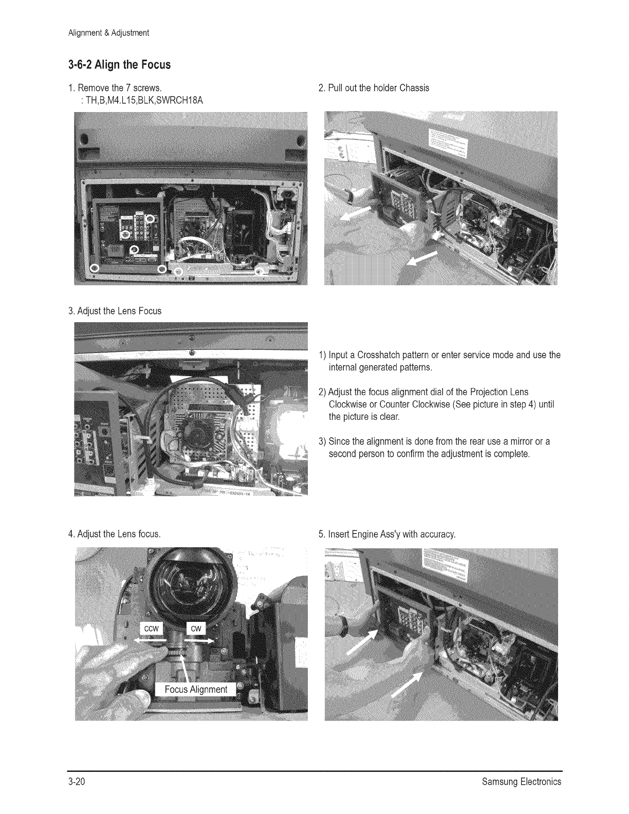
3-6-2 Align the Focus
1. Removethe 7 screws.
: TH,B,M4.L15,BLK,SWRCH18A
2. Pullout the holderChassis
3. Adjustthe Lens Focus
1) Inputa Crosshatchpatternor enterservicemodeanduse the
internalgeneratedpatterns.
2)Adjustthe focusalignmentdialof the ProjectionLens
Clockwiseor CounterClockwise(Seepicturein step4) until
the pictureis clear.
3)Sincethe alignmentis donefromthe rear usea mirroror a
secondpersonto confirmthe adjustmentis complete.
4. Adjustthe Lensfocus. 5. InsertEngineAss'ywithaccuracy.
3-20 SamsungElectronics

Exploded View & Part List
4. Exploded View & Part List
4-1 HLR6768WX/XAA
Yoncan searchfor the updatedpart codethroughITSELFwebsite,
URL:http://itself.sec.samsung.co.kr
/
MO006i
iT0852
r
T0i58j
Loc.Nol Code N01 I Description Specification Q'ty SA/SNA Remark
DIS7 AA61-60003J SPRING ETC-CS -,SUS304,-,-,OD6,N7,OD6,-, 1 S.N.A
M0006 BP63-00431A COVER-REAR 67L6,HIPS,HB,GRAY,TOP 1 S.A
M0006 BP63-00401A COVER-REARBOTTOM 50L6,HIPS,V0,GRAY 1 S.N.A
M0013 BP96-009380 ASSY COVERP-REARBOTTOM L6,HIPSV0,GR50 1 S.A
M0107 BP61-00892A BRACKET-PCB 50L3,SECC,TI.O,NTR,TOP(BUILT 1 S.N.A
M0107 BP61-00893A BRACKET-PCB 50L3,SECC,T1.0,NTR,BOT(BUILT 1 S.N.A
M0112 BP63-00429D COVER-FRONT 67L6,HIPS,HB,BLK,BKM1326R1,S 1 S.N.A
M0119 BP41-00124B PCBCONTROL HLP5063W,FR-4,2L,A,1.6T,245 1 S.N.A
M0256 BP96-00849F ASSY BRACKETP-MAIN PCB L3,L6,L7,SECC,T1 1 S.A
T0002 BP96-01024A ASSY COVERP-FRONTBOTTOM 67L6,HIPS,HB,G 1 S.A
T0003 BP96-0103OD ASSY COVER P-FRONT 67L6,SEA(L65A),HIPS,H 1 S.A
T0024 BP64-00384B KNOB-FAMILY L6,ABS,HB,GRAY,SVM-3012 1 S.N.A
T003O BP96-01027B ASSY COVER P-SIDE 67L6,HIPS,HB,GR503,LEF 1 S.N.A
T003O BP96-01028B ASSY COVER P-SIDE 67L6,HIPS,HB,GR503,RIG 1 S.N.A
T0053 BP67-00187A SCREEN FRESNEL 67W,1524*875,T2.0 1 S.A
T0054 BP67-00186A SCREEN LENTI 67W,1524*875,T2.1 1 S.A
T0057 BP64-00179A BADGE-BRAND ALL,ALT1.5,83,14,,BLK,SILIV 1 S.N.A
T0061 BP64-00385A WlNDOW-REMOCON 50L3,PC,VlOLET 1 S.N.A
T0062 BP61-00530A HOLDER-POWER 50L3,HIPS HB,GRAY 1 S.N.A
T0066 BP96-00535E ASSY COVER P-DUCT L6,HIPS HB,GRY 1 S.N.A
T0071 BP64-00382A INDICATOR-LED 50L3,ABS CLEAR (LG) 1 S.N.A
T0074 BP59-00071B REMOCON HURRICANE,TM76A,2OO*54*3O,ZlLOG 1 S.A
T0082 BP64-00309B WINDOWLED 50L3,ACRYL,2.0,half-mirror,SE 1 S.N.A
T0091 BP94-01713A ASSY PCBMISC-A/V SIDE HLR6768WX/XAA,L65 1 S.N.A
T0120 BP94-02215B ASSY PCB POWER HLR5067,HURRICANE,L64B,11 1 S.A
T0129 BP96-01198D ASSY ENGINE P-DLP 67L8,PHILIPS 132W,E22, 1 S.A
T0130 BP96-01061A ASSY COVERP-TERMINALBOARD 50L8,HIPSV0 1 S.N.A
T0132 BP94-02229A ASSY PCB MISC-DIGITAL HLR5078(L8),L65A,E 1 S.A
T0138 BP64-00383B KNOB-HOLDER L6,ABS,HB,GRAY,SVM3012 1 S.N.A
T0145 BP94-02228A ASSY PCB MISC-ANALOG HLR5078(L),L65A,EXC 1 S.A
T0158 BP96-009370 ASSY COVER P-MAIN L6ALL,HIPS, V0,GR503 1 S.A
T0175 BP96-01278A ASSY SPEAKERP 8ohm,L6(DLP)_VE,15W 2 S.A
T0186 BP96-01025B ASSY COVER P-GRILLE 67L6,HIPS,HB,GR503,S 1 S.N.A
T0245 BP94-01714A ASSY PCBMISC-KEYCONTROL HLR6768WX/XAA, 1 S.N.A
T0260 BP67-00215A MIRROR-FRONT Front mirror67",glass,1510 1 S.A
T0267 BP61-00938A BRACKET-MIRRORTOP 67L6,AL6063EXTR 1 S.N.A
T0268 BP94-01758D ASSY PCB MISC-RMCLED HLR6768WX/XAA,L65A 1 S.N.A
T0268 3903-000144 CBF-POWERCORD DT,US,BP3/Y,U(IEC013-RA) 1 S.A
T0514 BP61-00916A BRACKET-SUPPORT 67L6,SECC-1,T1.2,NTR,BAC 2 S.N.A
T0514 BP61-00918A BRACKET-SUPPORT 61L6,SECC-1,T1.6,NTR 2 S.N.A
T0524 BP63-00433A COVER-GRILLE 67L6,HIPS,HB,GR503,SV012P 1 S.N.A
T0527 BP61-01045A BRACKET-COVER L6,SECC-1,T1.2,NTR,BOTTOM 1 S.N.A
T0852 BP96-01026B ASSY COVER P-MIDDLE 67L6,HIPS,HB,GR503,S 1 S.N.A
T0903 BP61-00528A HOLDER-DUST 50L3,HIPS HB,GRAY 2 S.N.A
T0952 BP63-00294B COVERDUST-ASSY L6,HIPS,HB,GRAY 2 S.N.A
SamsungElectronics 4-I
Exploded View & Part List
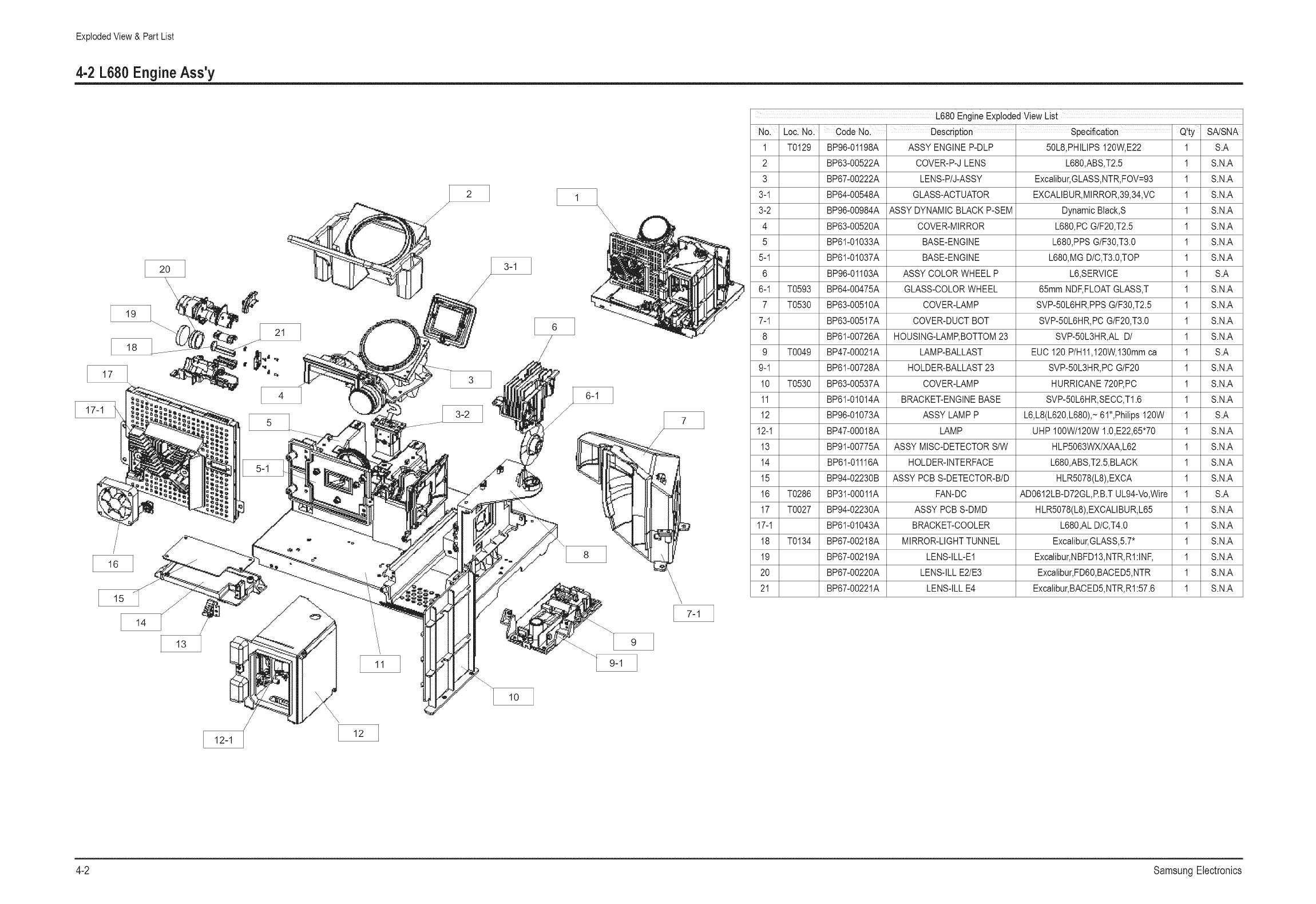
4-2 L680EngineAss'y
\\ \
\\\,
L680EngineExplodedViewList
No. Loc:No. CodeNo., Description SpeCification ' Q'ty' SA!SNA
1 T0129 BP96-01198A ASSY ENGINE P-DLP 50L8,PHILIPS 120W,E22 1 S.A
2 BP63-00522A COVER-P-J LENS L680,ABS,T2.5 1 S.N.A
3 BP67-00222A LENS-P/J-ASSY Excalibur, GLASS,NTR,FOV=93 1 S.N.A
3-1 BP64-00548A GLASS-ACTUATOR EXCALIBUR,MIRROR,39,34,VC 1 S.N.A
3-2 BP96-00984A ASSY DYNAMIC BLACK P-SEM Dynamic Black,S 1 S.N.A
4 BP63-00520A COVER-MIRROR L680,PC GIF20,T2.5 1 S.N.A
5 BP61-01033A BASE-ENGINE L680,PPS GtF30,T3.0 1 S.N.A
5-1 BP61-01037A BASE-ENGINE L680,MG D/C,T3.0,TOP 1 S.N.A
6 BP96-01103A ASSY COLOR WHEEL P L6,SERVICE 1 S.A
6-1 T0593 BP64-00475A GLASS-COLOR WHEEL 65mm NDF,FLOAT GLASS,T 1 S.N.A
7 T0530 BP63-00510A COVER-LAMP SVP-50L6HR,PPS GtF30,T2.5 1 S.N.A
7-1 BP63-00517A COVER-DUCT DOT SVP-50L6HR,PC GtF20,T3.0 1 S.N.A
8 BP61-00726A HOUSING-LAMP, BOTTOM 23 SVP-50L3HR,AL D/ 1 S.N.A
9 T0049 BP47-00021A LAMP-BALLAST EUC 120 P/H11,120W,130mm ca 1 S.A
9-1 BP61-00728A HOLDER-BALLAST 23 SVP-50L3HR,PC GtF20 1 S.N.A
10 T0530 BP63-00537A COVER-LAMP HURRICANE 720P,PC 1 S.N.A
11 BP61-01014A BRACKET-ENGINE BASE SVP-50L6HR,SECC,T1.6 1 S.N.A
12 BP96-01073A ASSY LAMP P L6,L8(L620,L680),- 61",Philips 120W 1 S.A
12-1 BP47-00018A LAMP UHP 100W/120W 1.0,E22,65"70 1 S.N.A
13 BP91-00775A ASSY MISC-DETECTOR S/W HLP5063WX/XAA,L62 1 S.N.A
14 BP61-01116A HOLDERqNTERFACE L680,ABS,T2.5,BLACK 1 S.N.A
15 BP94-02230B ASSY POD S-DETECTOR-BID HLR5078(L8),EXCA 1 S.N.A
16 T0286 BP31-00011A FAN-DC AD0612LB-D72GL,RB.T UL94-Vo,Wire 1 S.A
17 T0027 BP94-02230A ASSY POD S-DMD HLR5078(L8),EXCALIBUR,L65 1 S.N.A
17-1 BP61-01043A BRACKET-COOLER L680,AL D/C,T4.0 1 S.N.A
18 T0134 BP67-00218A MIRROR-LIGHT TUNNEL Excalibur, GLASS,5.7* 1 S.N.A
19 BP67-00219A LENSqLL-E1 Excalibur,NBFD13,NTR,R1:INF, 1 S.N.A
20 BP67-00220A LENSqLL E21E3 Excalibur, FD60,BACED5,NTR 1 S.N.A
21 BP67-00221A LENSqLL E4 Excalibur,BACED5,NTR,R1:57.6 1 S.N.A
4-2 SamsungElectronics
Electrical Part List
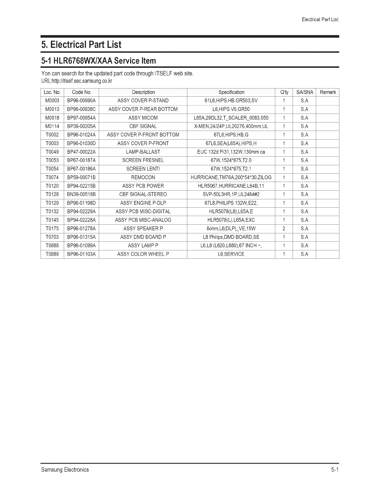
5. Electrical PartList
5-1 HLR6768WX/XAAService item
Yoncan searchfor theupdatedpart codethroughITSELFwebsite.
URL:http://itself.sec.samsung.co.kr
Loc. No. Code No. Description I specification Q'ty SA!SNA Remark
M0003 BP96-00990A ASSY COVER P-STAND 61L6,HIPS,HB,GR503,SV 1 S.A
M0013 BP96-00938C ASSY COVER P-REAR BOTTOM L6,HIPS V0,GR50 1 S.A
M0018 BP97-00954A ASSY MICOM L65A,29DL32,T_SCALER_0083,050 1 S.A
M0114 BP39-00205A CBF SIGNAL X-MEN,24/24P,UL20276,400mm,UL 1 S.A
T0002 BP96-01024A ASSY COVER P-FRONT BOTTOM 67L6,HIPS,HB,G 1 S.A
T0003 BP96-01030D ASSY COVER P-FRONT 67L6,SEA(L65A),HIPS,H 1 S.A
T0049 BP47-00022A LAMP-BALLAST EUC 132d P/31,132W,130mm ca 1 S.A
T0053 BP67-00187A SCREEN FRESNEL 67W,1524"875,T2.0 1 S.A
T0054 BP67-00186A SCREEN LENTI 67W,1524*875,T2.1 1 S.A
T0074 BP59-00071B REMOCON HURRICANE,TM76A,200*54*30,ZILOG 1 S.A
T0120 BP94-02215B ASSY PCB POWER HLR5067,HURRICANE,L64B,11 1 S.A
T0128 BN39-00518B CBF SIGNAL-STEREO SVP-50L3HR, 1P,UL2464#2 1 S.A
T0129 BP96-01198D ASSY ENGINE P-DLP 67L8,PHILIPS 132W, E22, 1 S.A
T0132 BP94-02229A ASSY PCB MISC-DIGITAL HLR5078(L8),L65A, E 1 S.A
T0145 BP94-02228A ASSY PCB MISC-ANALOG HLR5078(L),L65A, EXC 1 S.A
T0175 BP96-01278A ASSY SPEAKER P 8ohm,L6(DLP)_VE,15W 2 S.A
T0703 BP96-01315A ASSY DMD BOARD P L8 Philips,DMD BOARD,SE 1 S.A
T0888 BP96-01099A ASSY LAMP P L6,L8 (L620,L680),67 INCH -, 1 S.A
T0889 BP96-01103A ASSY COLOR WHEEL P L6,SERVICE 1 S.A
SamsungElectronics 5-1
Troubleshooting
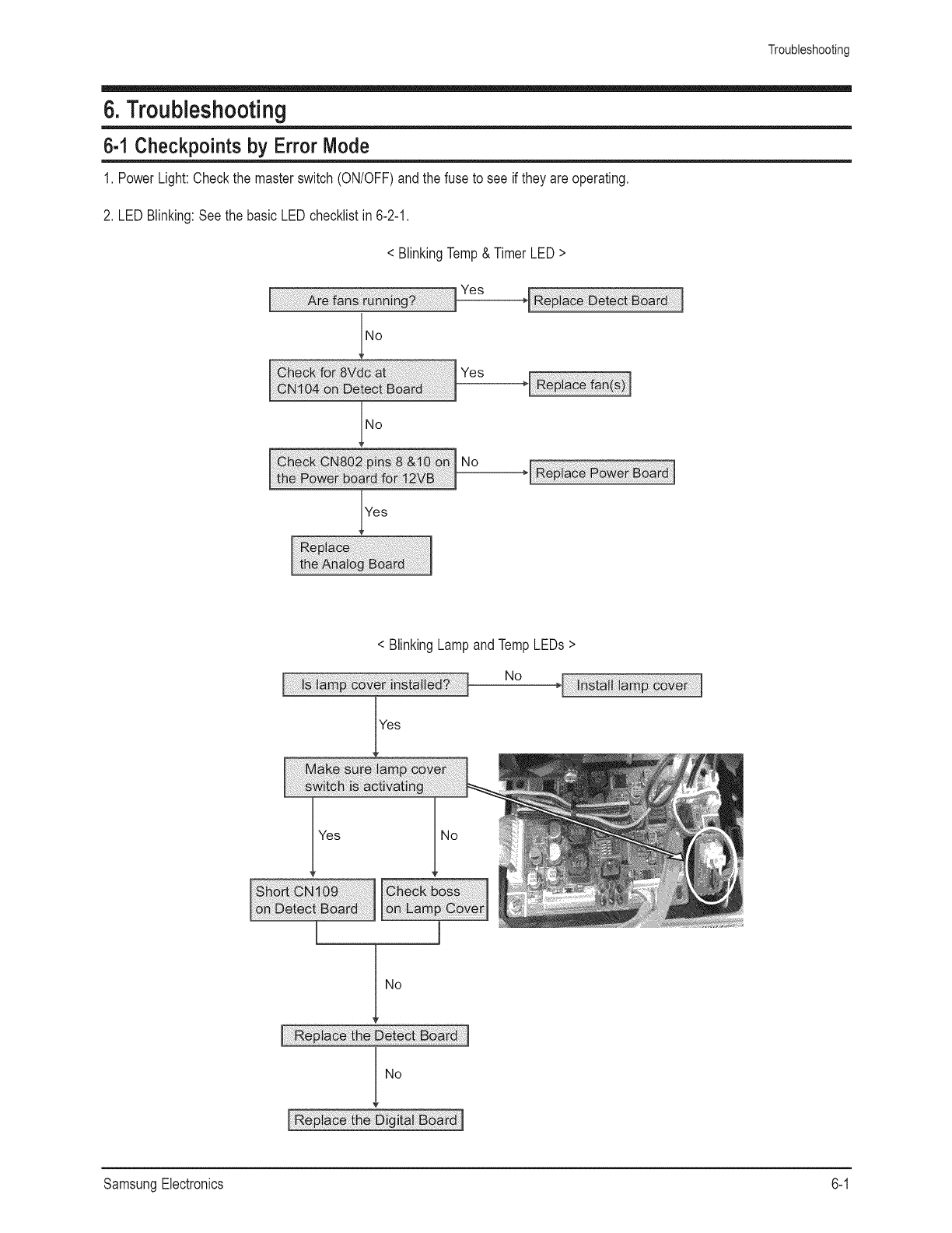
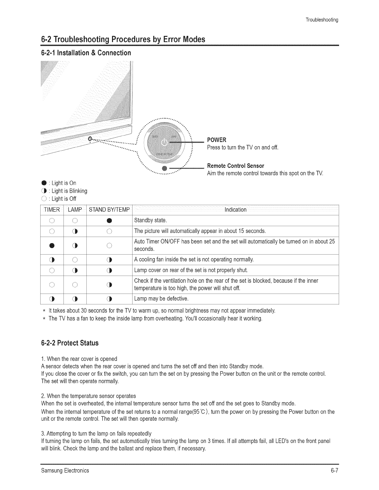
6. Troubleshooting
6-1 Checkpoints by Error Node
1, PowerLight:Checkthe masterswitch(ON/OFF)andthe fuseto see if theyareoperating,
2, LEDBlinking:Seethe basicLEDchecklistin6-2-1,
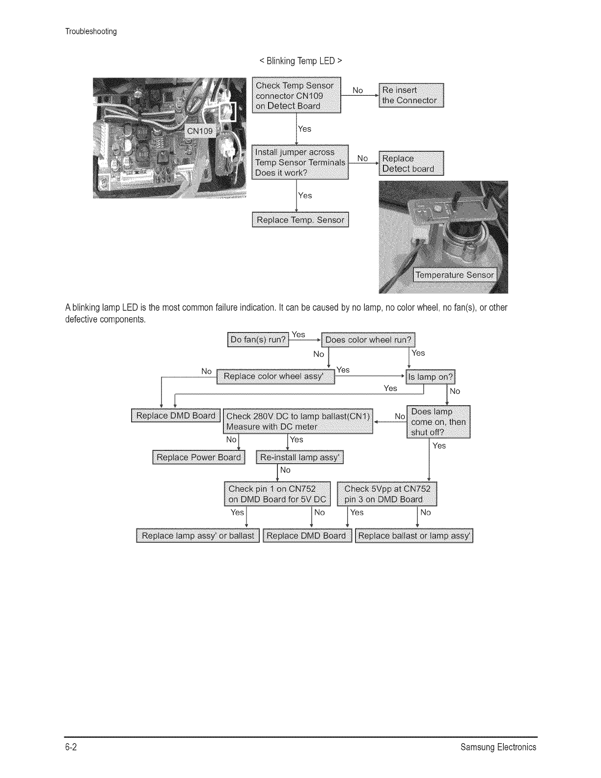
< BlinkingTemp& TimerLED>
Yes
Yes
No
Yes
< Blinking Lamp and Temp LEDs >
No
Yes
No
No
SamsungElectronics 6-1
Troubleshooting
< BlinkingTempLED>
Yes
A blinkinglampLED is the mostcommonfailureindication.Itcan be causedby no lamp,no colorwheel,no fan(s),orother
defectivecomponents.
Yes
_e1 1_obs _o
6-2 SamsungElectronics
Troubleshooting
3, Noise:
Internalnoisemaybe causedby aforeignsubstanceon the fan or drivingdevice.
For a DLPTV,the lampfan,DMDboardfan and colorwheelarevulnerableto noise.Sometimesthe connectorwire aroundthe
lampor DMDfan makescontactwith thefan, whilethe colorwheelis protectedinsidethe moduleandcannotmakecontactwith
any nearbywires. Howeverthe colorwheelsensoror the drive motormaycausenoiseby makingcontactwiththe colorwheel.
As the colorwheelusesan air bearingsystem,it hasa veryslightpossibilityof creatinginternalnoise.
Whenirregularnoiseoccursfor noparticularreason,checkthe insideof the TV for anyforeignsubstances.
The DLPprojectionTV maycausenoiseas the physicalscreenis emptyinside,causinga resonanceto a particularfrequency.
Thusa lowvibrationis nota malfunction.
Any 'creaking'noiseis mostlyfromthe structureof the deviceitself.Ashort, harshnoisemayoccurfroma distortionor
malformationdueto thermalexpansionbetweenthe metaljoints,screwsandloadedparts,respectively.Any intermittent'creaking'
noisecan be removedby looseningthescrews.
4. A blackscreenwiththe lampon: Replacethe DMDboard.
5. LinePattern:Regularlinepatternsoccurverticallyor horizontally:Replacethe DMDboard.
6. VoiceDistortion:Replacethe analogboard.
7. OutsideLight:This is not a productmalfunction,buta possibleinstallationor humanerror.Thisoccurswhen the projectedlight
fromthe surroundingilluminationreflectsontothe screen.Thisdisappearsas the TV startsoperatingandtheTV lampgets
brighter.However,youcan avoidoutsidelight by changingthe positionof the TV orthe installationangle.
Decreasingthe illuminationor changingthe indoorlightingmaywork.
8. ScreenFlip-over:
Enter Factorymodein DDP1011and performH-Flip(flip horizontally)andV-Flip(flipvertically).
The screenwill flip overhorizontallyor vertically.
SamsungElectronics 6-3

Troubleshooting
9, OtherScreenErrors:
i_ 40Verticallines 16pixelswide:
DDP1011or BGA,DMDpanelinterference,
Replacethe DMDboard
i_ HorizontalBaror No Raster:
Errorin DDP1011or the DMPpanel,
Replacethe DMDboard
i_ DottedVerticalBar:
Errorin RambusDram(IC403)or the soldering
Replacethe DMDboard
i_ Beehivemosaicpatternsallover the screen:
Errorin the LVDSReceiver(IC601)or the soldering
The H syncsignalsare nottransferredto DDP1011,
Replacethe DMDboard,
6-4 SamsungElectronics

Troubleshooting
6-1-1 Video Circuit Error Checking
m Basics:
- The DDP1011on the DMDboardhasa featureto displayinternaltest patterns.
- DNle,whichis an endport inthe digital board,has a featureto displayinternaltest patterns.
- The analogboardsendssignalsto ADV7401on the digitalboard.
- The analogboardis thefirst outputandthe digitalboardis the secondone,followedby DMD,whichis the final one.
[] DiagnosisBy Module
1.AccessServiceMode
(In Standbymode,press"Mute","1","8", "2" and"Power"to turn the screenon andenterservicemode)
2. Checkif thereis an errorin the DMDboard
DDP1011-->TESTPATTERN_ Pressthe rightarrowkey:
Optionsof FULLWHITE,BLACK,RED,GREENand BLUEPATTERNaredisplayedon the screen.
If"Pattern"doesnot appear,thisis a DMDboarderror.
3. Checkif thereis an errorin the digitalboardbeforethe DMD.
Whenthe DMDboardhasbeendeterminedto beerrorfree basedonthe test patterns:
FACTORYMODE_ DNle_ TESTPATTERNnormaldisplay:noerrorin the digitalboard.
If"Pattern"doesnot appear,you haveto checka Analogboardfirst,andchecka DMDBoardsecond,nextchecka Digital
Board.
4. Checkif thereis an errorin theAnalogBoard.
Checkfor a powersignalfrom the analogto the digitalboards.(Seethe circuitdiagrambelow).
_A
33VB
i
I _ii _
57_/R 70VB
Iltl] - -
CN4 I
,_ "'-ta_'----'1' 7'27Z1_uF
t 'X
SamsungElectronics 6-5
Troubleshooting
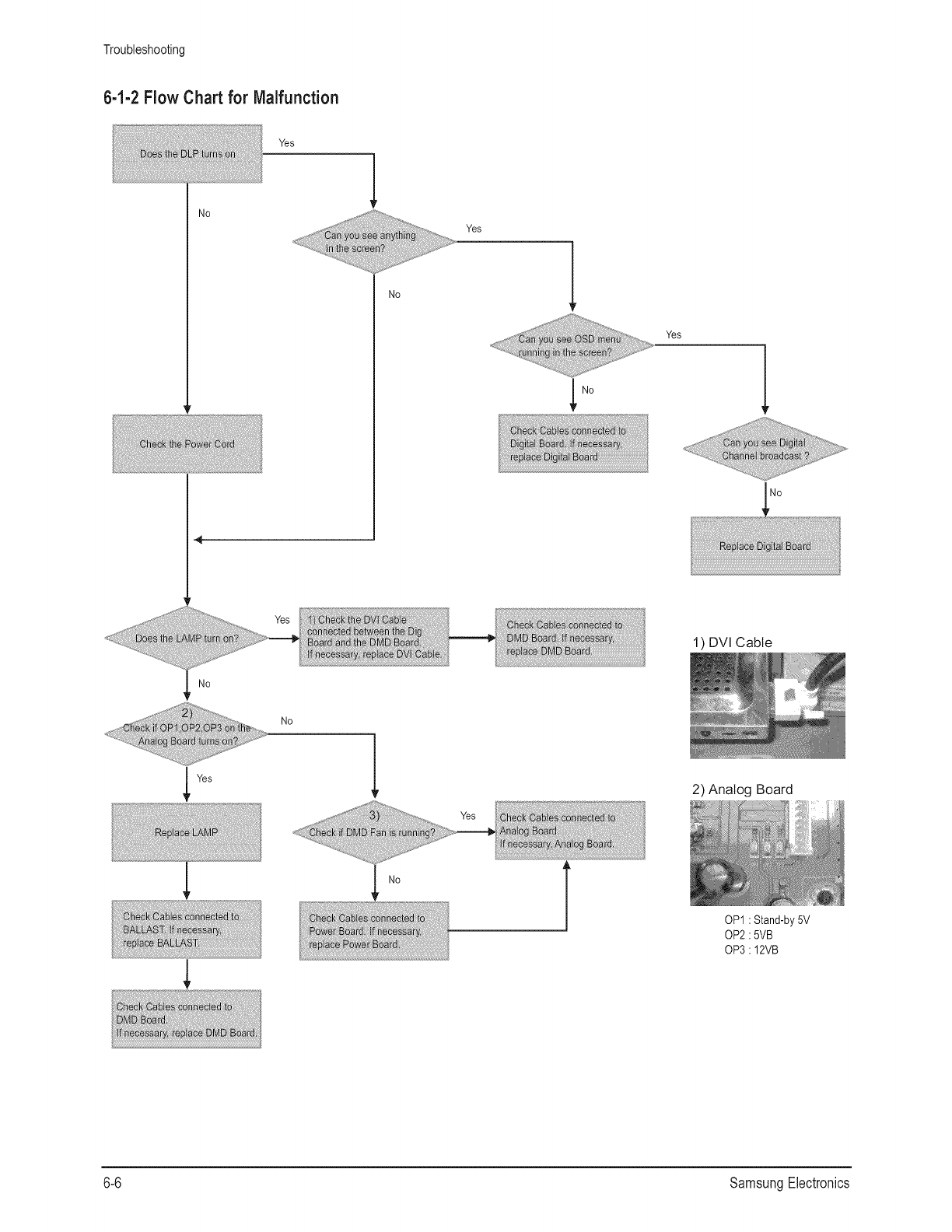
6-1-2 Flow Chart for Malfunction
Yes
No
No
Yes
No
Yes
No
No
Yes
No
1) DVI Cable
Yes
2) Analog Board
No
OP1 ' Stand-by5V
OP2 :5VB
OP3: 12VB
6-6 SamsungElectronics
Troubleshooting
6-2 Troubleshooting Procedures by Error Modes
6-2-1 Installation & Connection
•'Lightis On
(D ' Lightis Blinking
:) ' Lightis Off
POWER
Pressto turnthe TV on andoff.
Remote Control Sensor
Aimthe remotecontroltowardsthisspoton the TV.
TIMER LAMP: STANDBY/TEMP:' indication
( b ( b • Standbystate.
(b (D (b The picturewill automaticallyappearinabout 15seconds.
AutoTimerON/OFFhasbeensetandthe setwill automaticallybe turnedon in about25
• (D ( _ seconds.
(D (:) (D A coolingfan insidethe set is not operatingnormally.
( _ (D (D Lampcoveron rearof the set is not properlyshut.
Checkif the ventilationholeon the rearof the set is blocked,becauseif the inner
temperatureis too high,the powerwill shutoff.
(D (D (D Lampmaybedefective.
* Ittakesabout 30secondsfor the TV to warmup, so normalbrightnessmaynot appearimmediately.
* The TV hasa fan to keepthe insidelampfromoverheating.You'lloccasionallyhearit working.
6-2-2 Protect Status
1.Whenthe rearcoveris opened
Asensordetectswhen the rearcoveris openedandturnsthe set offand theninto Standbymode.
If you closethe coverorfix the switch,you canturn the seton by pressingthe Powerbuttononthe unit or the remotecontrol.
The setwill thenoperatenormally.
2. Whenthe temperaturesensoroperates
Whenthe set is overheated,the internaltemperaturesensorturnsthe set offandthe set goesto Standbymode.
Whenthe internaltemperatureof the set returnsto a normalrange(95°C), turn the poweron by pressingthe Powerbuttononthe
unit orthe remotecontrol.Thesetwill thenoperatenormally.
3. Attemptingto turn the lamponfails repeatedly
If turningthe lamponfails, the setautomaticallytriesturningthe lampon 3 times.Ifall attemptsfail,all LED'son thefront panel
will blink.Checkthe lamp andthe ballastandreplacethem, if necessary.
SamsungElectronics 6-7
Troubleshooting
6-3 Troubleshooting Procedures by ASS'Y
6-3-1 Check Lamp & Ballast
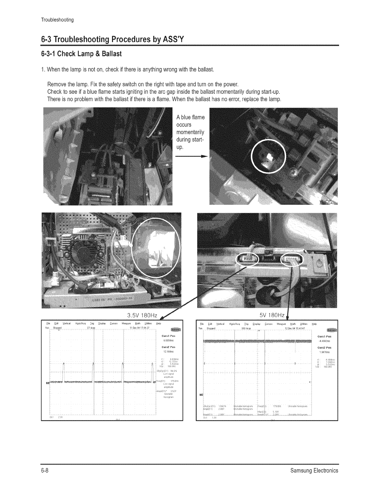
1.Whenthe lamp is not on, checkif there is anythingwrongwiththe ballast.
Removethe lamp.Fixthe safetyswitchon the rightwith tapeandturn on the power.
Checkto see if a blueflamestartsignitingin the arc gapinsidethe ballastmomentarilyduringstart-up.
Thereis no problemwiththe ballastif thereis a flame.Whenthe ballasthasno error,replacethe lamp.
A blueflame
occurs
momentariiy
duringstart-
up.
,/,, cf _, Ja,
6-8 SamsungElectronics
Troubleshooting
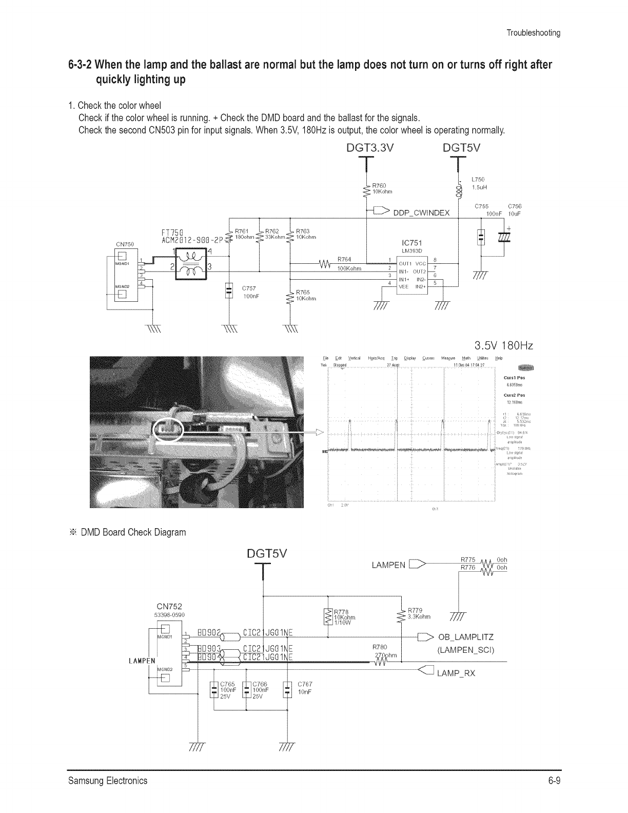
6-3-2 When the lamp and the ballast are normal but the lamp does not turn on or turns off right after
quickly lighting up
1. Checkthe colorwheel
Checkif the colorwheel is running.+ Checkthe DMDboardandthe ballastfor the signals.
Checkthe secondCN503pinfor inputsignals.When3.5V,180Hzis output,the colorwheelis operatingnormally.
DGT3.3V DGT5V
FT750
CN750 ACN2012-900-2P_
R760
10Kohm
_" DDP CW_NDEX
IC75I
LM393D
L750
1 5uH
C755 C756
100nF 10uF
File _di Vetical Hodzlbcq !ri_ Disr,la_
3.5V 180Hz
11n_GFi417 04 _7
cu_sl Pos
C_2 Pes
/2 168ms
i_ , u-vl,
-_ DMDBoardCheckDiagram
CN752
53398-0590
7_ T
DGT5V
R775 _AA_
LAMPEN _
[_L_R778 _L R779 i
I<_1 t 0Kohm
i 10W I 3 3Kohn, OB LAMPLITZ
R780 (LAMPENSCI)
LAMP_RX
C767
10nF
72
SamsungElectronics 6-9

Block Diagram
7. Block Diagram
7-1 Overall Block Diagram
Anynet, G-Link
HDMI/PC
IEEE1394/Anynet
Optical/Gemstar-IR
RF In(Air,Cabl_
CableCard
AlVIn 1 2 3
S-Video 1 2 3
Component 1,2
,,_ A/V Out
RS-232C In
PC/DVI Audio In
AC
SamsungElectronics 7-1
Block Diagram
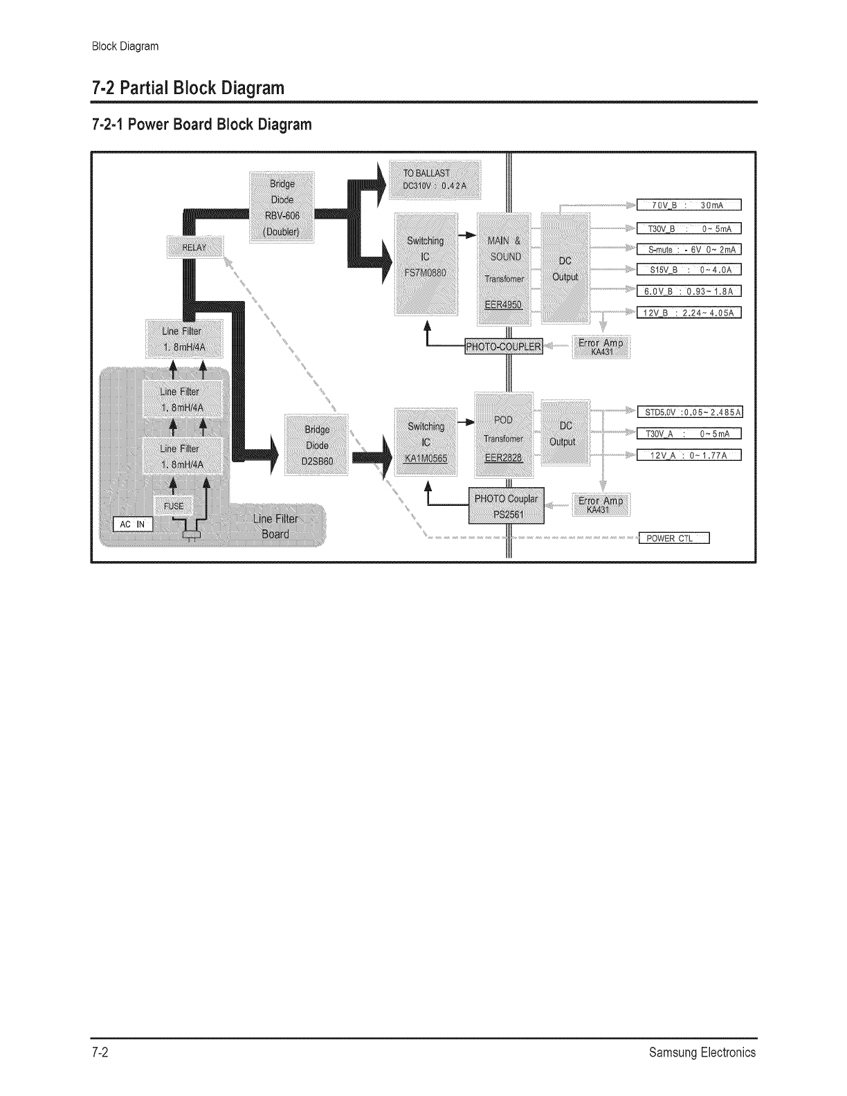
7-2 Partia{ Block Diagram
7-2-1 Power Board Block Diagram
70VB : 30mA 1
T30VB : 0~SmA]
S-mute : - 6V 0~ 2mA ]
S15VB : 0-o4:0A ]
6.0V_B : 0.93~1:8A J
POWER CTL ]
7-2 SamsungElectronics
Block Diagram
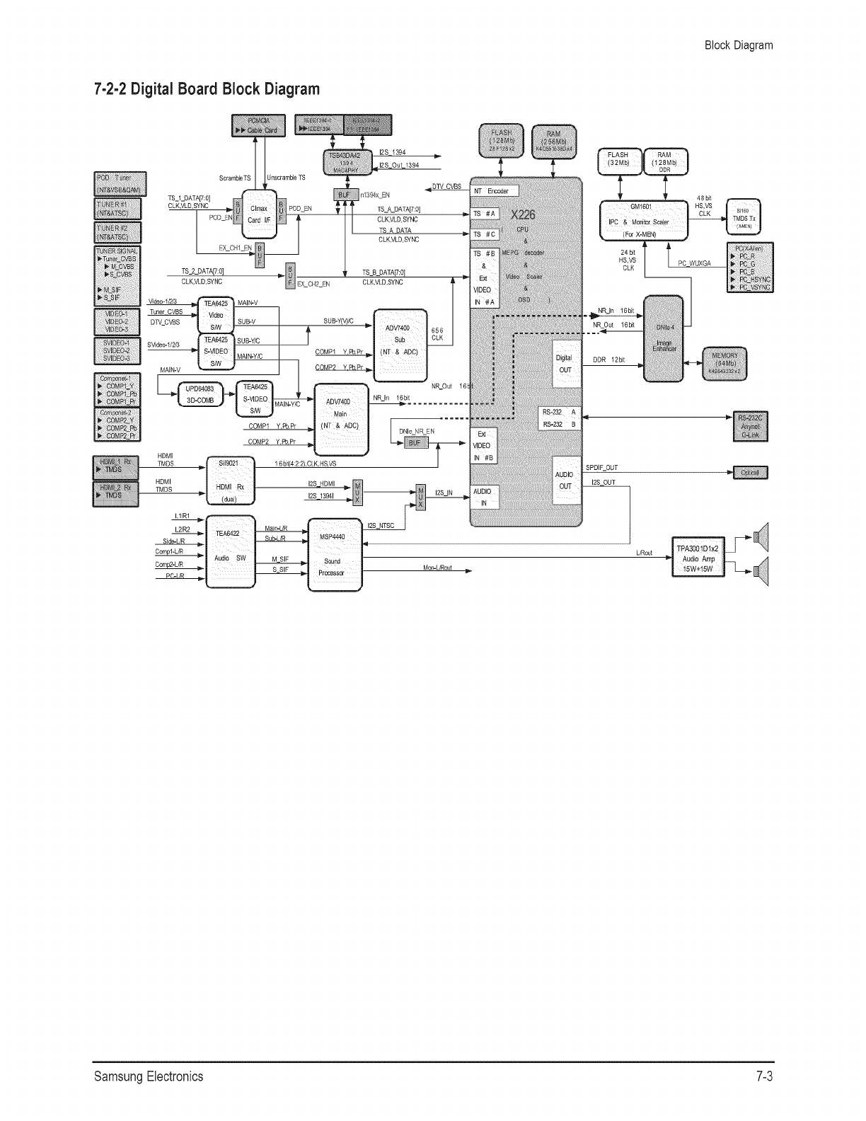
7-2-2 Digital Board Block Diagram
TS_I_OATA[/:0]
CLK,VLD,SYNC
HDMI
TMDS
HDMI
TMDS
MAIN-V
L1/R1
L2?R2
Side-L/R
ScrambleTS Unscramble TS
MAIN-V
TS_2_DATA[7:0]
CLK,VLD,SYNC
COMP1
COMP2
12S_1394
12S_OUL1394
TS_A_DATA[7:0]
CLK,VLD,SYNC
CLK,VLD,SYNC
TS_B_DATA[7:0]
CLK,VLD,SYNC
suB-Y(V)/C
COMP1
NROut 161
NR In 16bit
bNle NR EN
1 6bit(4:2: 2/,CLK,HS,VS
12S 13941
NR_Out 16bit
DDR 12bit
PDIF_OUT
12S OUT
SamsungElectronics 7-3
Block Diagram
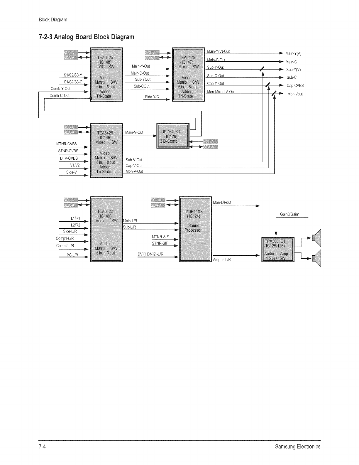
7-2-3 Analog Board Block Diagram
$1/$2/$3-Y
S1/$2/S3-C
Comb-Y-Out
Comb-C-Out
MTNR-CVBS
STNR-CVBS
DTV-CVBS
V1N2
Side-V
Main-Y-Out
Main-C-Out
Sub-YOut
Sub-COut
Side-Y/C
Main-V-Out
Sub-V-Out
Cap-V-Out
Mon-V-Out
Main-Y(V)-Out
Sub-Y-Out
Sub-C-Out
CaD-Y-Out
Mort-Mixed-V-Out
Main-Y(V)
Main-C
Sub-Y(V)
Sub-C
_ Cap-CVBS
7L__ Mon-Vout
L1/R1
L2/R2
Side-L/R
Compl-L/R
Comp2-L/R
PC-L/R
Main-L/R
MTNR-StF
STNR-StF
DVt(HDMI2)-L/R
Mon-L/Rout
Amp-ln-L/R
Gain0/Gain1
7-4 SamsungElectronics

Block Diagram
7-2-4 DMD Board Block Diagram
Lam
Power Good
Reset M
CLKRX
DATRX TMDS
RGB ODD
DMD Ctrl
Lvds Bus Master A/B
Lvds Bus Slave A/B
100Mhz
Lamp En
-- Lamp Litz
-- CW Index
_et
3.3 V output ]
>l VCM Actuator
=_l DB Actuator
_l Detector Circuit
[ 24 P con
SamsungElectronics 7-5

03
3
O3
[77
0
O3
,oo
KEY CONTROL
FRONT LED
FAN
ANALOG
DIGITAL
DMD
DETECT
FAN1 FAN2
POWER
SIGNAL
Dynamic Black
ACTUATOR
COLOR WHEEL
TEMP SENSOR
BALLAST
POWER
0
3
ED

r_
Go
3
CQ
m
r_
C_
o
c_
O
_D
_D
CD
O
€_
C1R
c_
€_
U_J
O
Cll

PCB Diagram
9. PCB Diagram
9-1 Power Board
9-1-1 Assy Power Board
m DCPowerSupply
(SuppliesDCpowerto the analogPCB,Theanalogboardis responsiblefor the powersupplyto the digital/DMDboard,)
9-1-2 Names & Roles of Key Parts
* CN801' Suppliespower(DC220-400v)to the ballast
* GT801' Anti-lightningwire connectedto the digital board.The anti-lightningwire shouldbe installedfor safetypurposes.
* PD802S' Inlettypeof terminalthat is connectedto theAC powercable.
SamsungElectronics 9-1
PCB Diagram
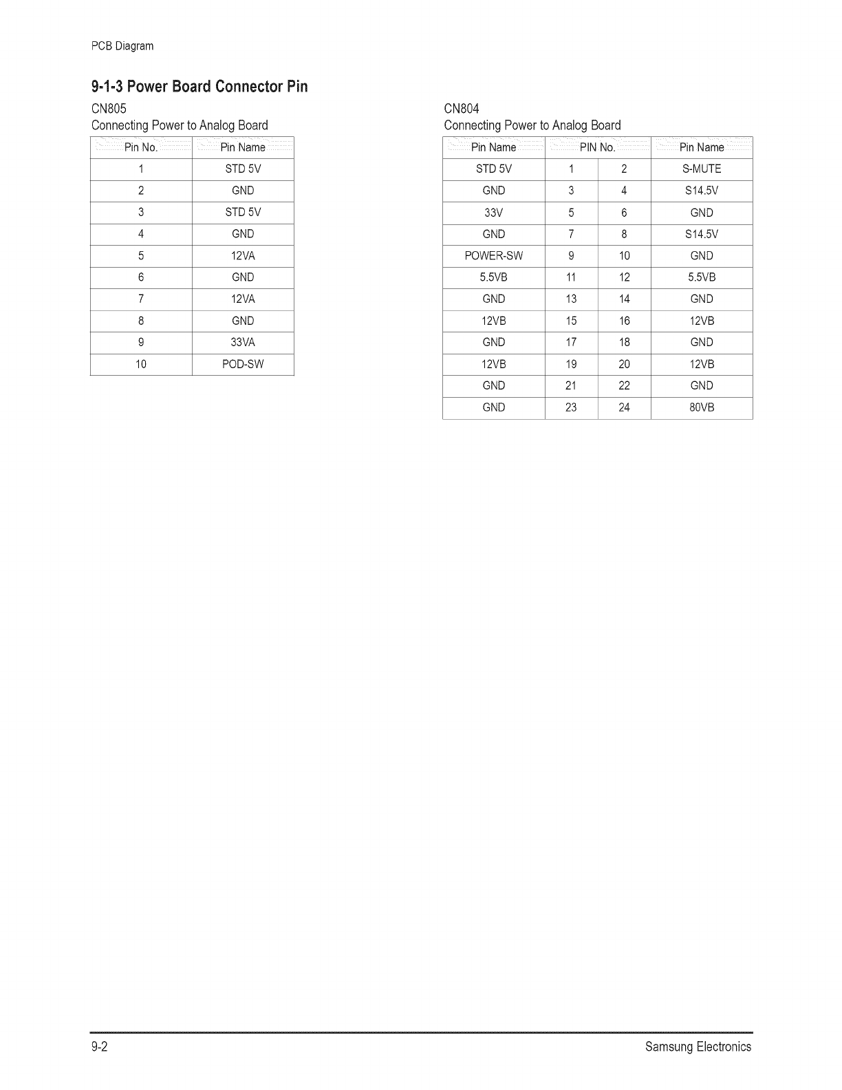
9-1-3 Power Board Connector Pin
CN805
Connecting Power to Analog Board
Pin No...... Pin Name
1 STD5V
2 GND
3 STD5V
4 GND
5 12VA
6 GND
7 12VA
8 GND
9 33VA
10 POD-SW
CN804
Connecting Power to Analog Board
Pin Name , PIN Nol Pin Name
STD 5V
GND
33V
GND
POWER-SW
5.5VB
GND
12VB
GND
12VB
GND
GND
1 2
3 4
5 6
7 8
9 10
11 12
13 14
15 16
17 18
19 20
21 22
23 24
S-MUTE
S14.5V
GND
S14.5V
GND
5.5VB
GND
12VB
GND
12VB
GND
80VB
9-2 SamsungElectronics

PCB Diagram
9-2 Digital Board
9-2-1 Assy Digital Board
III All DigitalVideoProcessing
II OSD/Menu
II ResetSwitch(Resetto the CPU)
II Connectedwith PODchannelBoard.
9-2-2 Names & Roles of Key Parts
* CableCard:
CableCARDis a nationwidestandardsystemthatallowsyourlocalcable TV providerto supplyyou withan accesscard
customizedto your account.Thiscard allowsthe TV to receive,decodeandunscramblethe premiumdigitalchannelsincludedin
yourcableTV subscriptionwithoutthe use of a cable box.
* HighDefinitionMultimediaInterface:
The HDMITM (High DefinitionMultimediaInterface)supportsuncompressedstandardandhighdefinitiondigitalvideoformatsand
existingdigitalmulti-channelaudioformats.
* G-Link:
Thisjackis usedby the TV GuideOnscreensystemof the TV to controlexternalanalogdevicessuchas VCRs,cableboxes,
satellitereceivers.
* D-Net(IEEE1394):
Thesejacks allowtheTV to connectto externalIEEE 1394digitalproductsby meansof asinglecable.
SamsungElectronics 9-3
PCB Diagram
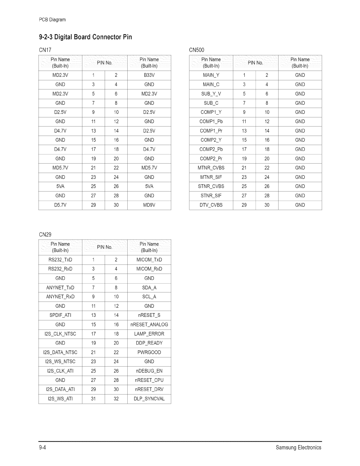
9-2-3 Digital Board Connector Pin
CN17
Pin Name ' I Pin Name
(Buit,ln)N N0- (Built'In)
MD2.3V
GND
MD2.3V
GND
D2.5V
GND
D4.7V
GND
D4.7V
GND
MD5.7V
GND
5VA
GND
D5.7V
1 2
3 4
5 6
7 8
9 10
11 12
13 14
15 16
17 18
19 20
21 22
23 24
25 26
27 28
29 30
B33V
GND
MD2.3V
GND
D2.5V
GND
D2.5V
GND
D4.7V
GND
MD5.7V
GND
5VA
GND
MD9V
CN500
Pin Name I Pin Name
(Built-In) N NO (Built-In)
MAIN_Y
MAIN_C
SUB_Y_V
SUB_C
COMPI_Y
COMPI_Pb
COMPI_Pr
COMP2_Y
COMP2_Pb
COMP2_Pr
MTNR_CVBS
MTNR_SIF
STNR_CVBS
STNR_SIF
DTV_CVBS
1 2
3 4
5 6
7 8
9 10
11 12
13 14
15 16
17 18
19 20
21 22
23 24
25 26
27 28
29 30
GND
GND
GND
GND
GND
GND
GND
GND
GND
GND
GND
GND
GND
GND
GND
CN29
Pin Narne i [:: I Pin Name
(Built-In) EI1'_r_o (Built-In)
RS232_TxD
RS232_RxD
GND
ANYNET_TxD
ANYNET_RxD
GND
SPDIF_ATI
GND
12SCLK NTSC
GND
12S_DATA_NTSC
12SWS NTSC
12S_CLK_ATI
GND
12S_DATA_ATI
12SWS ATI
1 2
3 4
5 6
7 8
9 10
11 12
13 14
15 16
17 18
19 20
21 22
23 24
25 26
27 28
29 30
31 32
MICOM_TxD
MICOM_RxD
GND
SDA_A
SCL_A
GND
nRESET_S
nRESET_ANALOG
LAMP_ERROR
DDP_READY
PWRGOOD
GND
nDEBUG_EN
nRESET_CPU
nRESET_DRV
DLP_SYNCVAL
9-4 SamsungElectronics
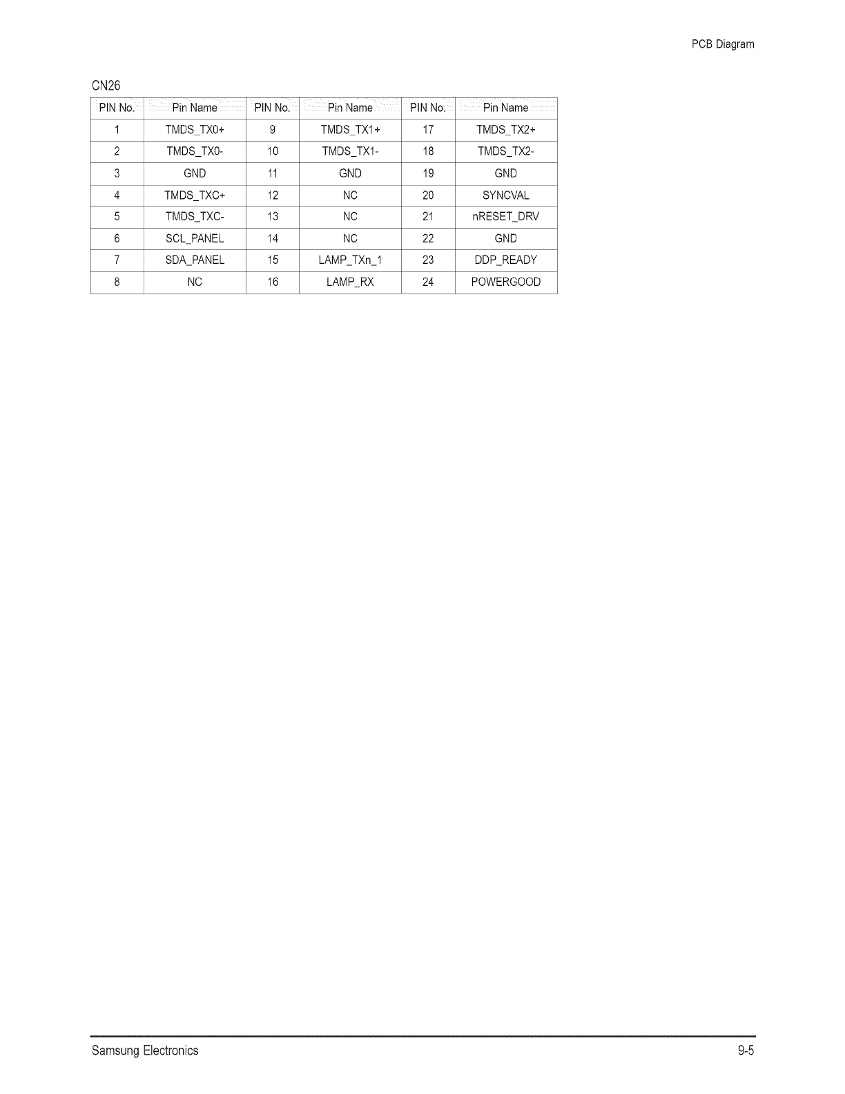
CN26
PiNNo. PinName PiNNo.'Pin Name PiN Nol ' PinName
1
2
3
4
5
6
7
8
TMDS_TX0+ 9 TMDS_TXI+ 17 TMDS_TX2+
TMDS_TX0- 10 TMDS_TX1- 18 TMDS_TX2-
GND 11 GND 19 GND
TMDS_TXC+ 12 NO 20 SYNOVAL
TMDS_TXC- 13 NO 21 nRESET_DRV
SOL_PANEL 14 NO 22 GND
SDA_PANEL 15 LAMP TXn 1 23 DDP_READY
NO 16 LAMP_RX 24 POWERGOOD
PCB Diagram
SamsungElectronics 9-5

PCB Diagram
9-3Ana(og Board
9-3-1 Assy Analog Board
Distributessupplyvoltagefromthe PowerBoardto DigitalBoardand DMDBoard.
m TransfersTurn-onCommand to Digitaland PowerBoard.
m Encompassesthe majorityof theAudioCircuit
m AnalogVideoSwitching/Processing
m AnalogAudioSwitching/Processing
m 3D CombProcessing
9-3-2 Names & Roles of Key Parts
* CN260: Connectedto the detectboard
* CN4,CN5: Connectedto the powerboard- receivesthe secondpowersourcegeneratedonthe powerboard.
* CN259: Sendsthe powersourcefromthe analogto the digitalboard.
* CN20: Thisis a controlsignalterminalthatconnectsbetweenthe analoganddigitalboards.
* CN257: Thisis an AVsignalterminalthatconnectsbetweenthe analoganddigital boards.
9-6 SamsungElectronics

9-3-3 Analog Board Connector Pin
CN259
Pin Name ' I Pin Name
(Buit,ln)N N0. (Built'In)
MD2.3V
GND
MD2.3V
GND
D2.5V
GND
D4.7V
GND
D4.7V
GND
MD5.7V
GND
5VA
GND
D5.7V
1 2
3 4
5 6
7 8
9 10
11 12
13 14
15 16
17 18
19 20
21 22
23 24
25 26
27 28
29 30
B33V
GND
MD2.3V
GND
D2.5V
GND
D2.5V
GND
D4.7V
GND
MD5.7V
GND
5VA
GND
MD9V
PCB Diagram
CN257
Pin Name IPin Name
(auittqn) NN0. (Built-In)
MAIN_Y
MAIN_C
SUB Y V
SUB_C
COMPI_Y
COMPI_Pb
COMPI_Pr
COMP2_Y
COMP2_Pb
COMP2_Pr
MTNR_CVBS
MTNR_SIF
STNR_CVBS
STNR_SIF
DTV_CVBS
1 2
3 4
5 6
7 8
9 10
11 12
13 14
15 16
17 18
19 20
21 22
23 24
25 26
27 28
29 30
GND
GND
GND
GND
GND
GND
GND
GND
GND
GND
GND
GND
GND
GND
GND
CN20
Pin Name ' I Pin Name
(Buit'ln)N N0. (Built'In)
RS232_TxD
RS232_RxD
GND
ANYNET_TxD
ANYNET_RxD
GND
SPDIF_ATI
GND
12S CLK NTSC
GND
12S_DATA_NTSC
12S WS NTSC
12S_CLK_ATI
GND
12S_DATA_ATI
12S WS ATI
1 2
3 4
5 6
7 8
9 10
11 12
13 14
15 16
17 18
19 20
21 22
23 24
25 26
27 28
29 30
31 32
MICOM_TxD
MICOM_RxD
GND
SDA_A
SCL_A
GND
nRESET_S
nRESET_ANALOG
LAMP_ERROR
DDP_READY
PWRGOOD
GND
nDEBUG_EN
nRESET_CPU
nRESET_DRV
DLP_SYNCVAL
CN4
Pin Name, PIN Nol Pin Name
5VA
GND
33VB
GND
POWER_SW
5.7VB
GND
12VB
GND
12VB
GND
GND
1 2
3 4
5 6
7 8
9 10
11 12
13 14
15 16
17 18
19 20
21 22
23 24
POWER_MUTE
S16VB
GND
S16VB
GND
5.7VB
GND
12VB
GND
12VB
GND
70VB
SamsungElectronics 9-7

PCB Diagram
CN5
Pin Nol I Pin Name
1 5VA
2 GND
3 5VA
4 GND
5 12VA
6 GND
7 12VA
8 GND
9 NC
10 POD_SW
CN11
ConnectingfrontLED indicators
Pin No. Pin Name
1 LED1
2 KEY1
3 KEY2
4 SDA_M1
5 SCL_M1
6 12VB
7 GND
CN17
Connectingthe IR signal
Pin Nol I Pin Name
1 IR
2 GND
3 5VA
CN9
Connecting and transmitting Audio signal to Speaker
Pin No. Pin Name
1 GND
2 L-OUT
3 GND
4 L-OUT
CN16
Connectingthe PowerandControlSignalto the PODFan
PinNol PinName
1 FAN_ERROR
2 GND
3 8VA_FAN
CN260
Pin
1
2
3
4
5
6
7
8
9
10
11
12
No: Pin Name
GND
GND
12VB
12VB
GND
SDA_M1
SCL_M1
GND
5VA
GND
70VB
GND
9-8 SamsungElectronics
PCB Diagram
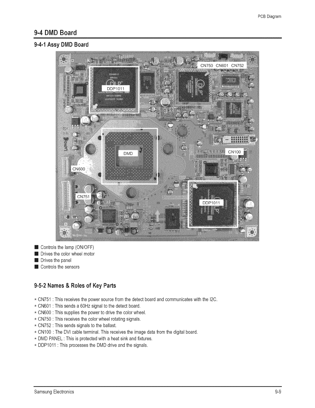
9-4 DMDBoard
9-4-1 Assy DMD Board
Controlsthe lamp(ON/OFF)
m Drivesthe colorwheelmotor
m Drivesthe panel
m Controlsthe sensors
9-5-2 Names & Roles of Key Parts
* CN751
* CN601
* CN600
* CN750
* CN752
* CN100
: Thisreceivesthe powersourcefromthe detectboardandcommunicateswiththe 12C,
: Thissendsa 60Hzsignalto the detect board,
: Thissuppliesthe powerto drivethe colorwheel,
: Thisreceivesthe colorwheel rotatingsignals.
: Thissendssignalsto the ballast.
: The DVlcable terminal.This receivesthe imagedatafrom thedigitalboard.
* DMDPANEL: Thisis protectedwitha heat sinkandfixtures,
* DDP1011: Thisprocessesthe DMDdriveandthe signals.
SamsungElectronics 9-9
Schematic Diagram
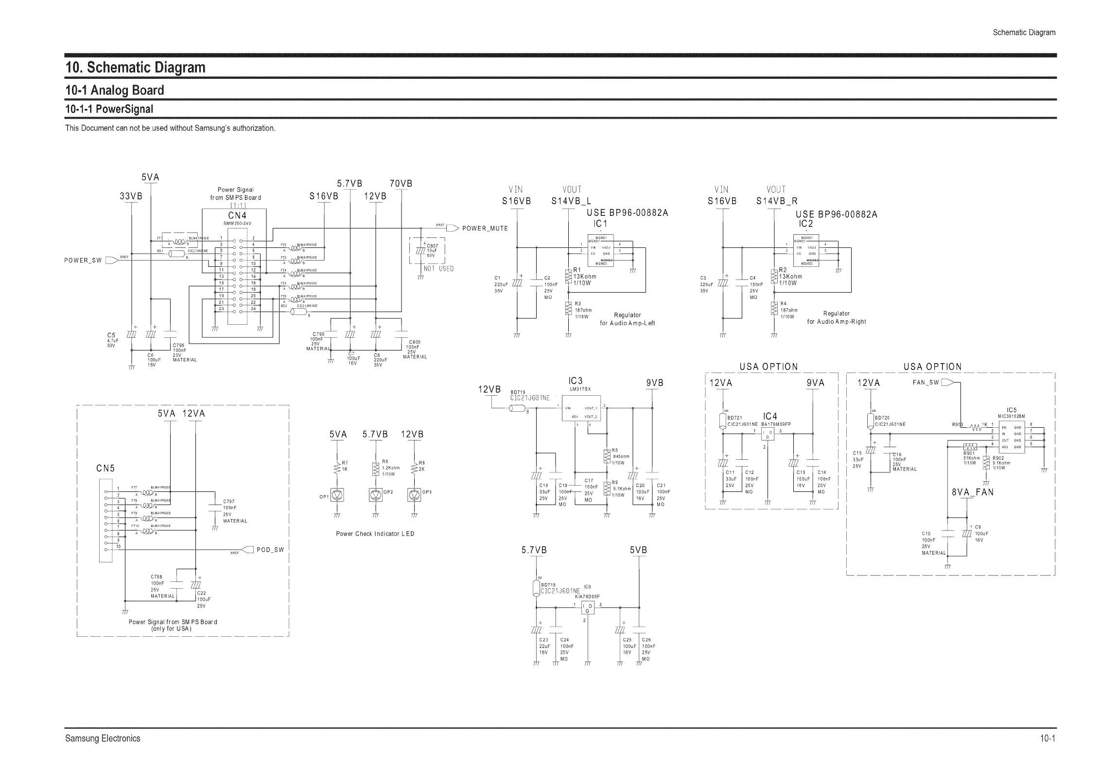
10. Schematic Diagram
10-1 Analog Board
10-1-1 PowerSignal
This Document can not be used without Samsung's authorization.
5VA
33VB
POWER SW _XREF
c5
47uF
50V
Power Signal
from SM PS Board
[1:1
[ s>l
FTr---- _ ....
,;oo- T
7y_o o
qT_o o-qT'
-- 17 o o 18
-- OO--_
19 20
.......... O......
--_ _ o 2T
• F
C6 25V
100uF MATERIAL
16V
5.7VB 70VB
S16VB 12VB
F__ --
'J MATERIA'tC'_ ' _MC_
. ,e_ !;ou_MATER,AL
35V
VIN V1N VOUI
S16VB S16VB S14VB_R
USE BP96-OO882A
162
rl _7} xREr[]]]:>-_ POWER MUTE
+C807
o: usED
c1
220uF
35V
CN5
5VA
C798
100nF
25AVERIAT
12VA
AC797
100nF
_A_ER,AL
+
c22
100uF
25V
Power Signal from SM PS Board
(only for USA)
....<::::::::::::]PODSW
5VA 5.7VB 12VB
7
!
OP1
Power Check Indicator LED
>R8
_2K
OP3
5.7VB
VOU[
S14VB_L
- USE BP96-00882A
ICl
li R1
T.ow
7_ for Audio Amp-L eft
IC3 9VB
LM317SX
I
11::;_m
-ZKo,m02o
11,10w_o°uF
LZ_
C21
100nF
25V
MO
5VB
KIA78D05F
C3
220uF
35V
_C4
100nF
;R2
Jl/10W I
R4
187ohm
I/low Regulator
for Audio Amp-Right
USA OPTION
12VA 9VA
I_
:11 c12
3uF 100nF
5V 25V
BD721 IC4
CIC21J601NE BA178M09FP
_1 MO
C15
33uF
25V
12VA
USA OPTION
FAN SW _ IC5
R90 ! .........
ADJ G_D
R901
51Kohm R902
_r T1/10W 9 1Kohm
8VA_FAN
C10 -- -- 100uF
100nF 16V
25V
MATERI
SamsungElectronics 10-1
Schematic Diagram
10-1-2 AV_Input
This Document can not be used without Samsung's authorization.
Power
Signal
COMP2 DET_ ....
PC_LIN
PC_RIN
DVLRIN
ANYNET_RX
RS232 TX
L60_
I 112{
100
100
R102
JA1
UJ%19901H
L 10_6_10uH
>Sl c
Y
>R1
> VI_DET
> Sl_DET
> S2_DET
R2
>V2
L2
> V2 DET
C
> S2Y
MON VOUT
MON ROUT
MON LOUT
_DET
Y
_Pb
Pr
R
L
L
R
Pr
OMP2_-Y
_OUT
DVI_LIN
> ANYNET TX
RS232 RX
From SideAV Board Assy
CN258
SIDE_Y
SIDE_C
SIDE_V
SIDE_L
SIDE_R
SIDE_SDET
SIDE_VDET
OPTICAL OUT [_:_0 \/_/ R104
5VB
03
0114
100nF
_vr
JA2
OP [](:AL OUl
10-2 SamsungElectronics

Schematic Diagram
10-1-3 AV_Switching
This Document can not be used without Samsung's authorization.
12V_OPTION 8V_6425
L3OO
01021J60 G
5 8V_6425
M AT E RIALTfT 7_T 7_T 7_T T_ MATERIAL
_;3Icd_I,}6olNEY/C
Power
Signal
ADDR:96h
8V_6425
[NoL in Usedl
Use in PAL mode(, to bypass 3D Comb block
,.z _z
7
_5_[[[_> SUB Y
_R_[[][_> SUB C
' _ MAIN Y
_[[[[3> MAIN C
I _ CAPY OUT
_ _ MON MIXED VOUT
8V_6425
L304
C:[C21J60 N
SDA A _ R343/V_0° I cs30 _0331
188uF _00nF
SCL A []_ x_F _346_/_?_ IC3042'_iv ......[.................
MTNR CVBS [_:>5_ lov_ ITEA6425D 7/7 T/_T
10uF 0334 _ _o
_XRE_ 16V _ 0337 1 L _ R3_!V_[[[[> MAIN V OUT
STNR CVBS _ _o_F_+ _ _ i_
IT XREF
.... _3_,0003,0,0_ _ i_ c>su_vo_m
we> _ _w _,_ _iii° _3_ _>CA_V°_m
DTV CVBS _ I /W_!.....................
xR_ R360 100 0343
SIDE V D_'9
:_V_,o_ 03. '
;°/vn_ CVBS Switching
9VB
..... AUDIO
SWITCHING
_c_o_ __,oo ...._ SDA_A
_=A_ o-,o............................-_--c_---_#V_[ _'#V_ _°° _3,0 _, "_<C] SCL_A
X_R_39 A..1K C324 _ 10UF _ ............... __ R1
L1 L_VV__ _ _ _°_
L2 _r-_;4_ ^^_Kc_ ,ooF 'L2 R2 _4_R 2
IDVI_LIN___',AA I..... C %1_F..... _..... LN3C _ ___"2......... R 45 I _REf....................................................................DVI_RI_
Si D ELL _1_+1 .... L4 R4 1_90 037 __ S I_D_EC_ R
COMPI_I_ __
COUP2_l_ __
R354
SUB_L _ .... o
L5 R5 "18
L6 R6 17 0336 10uF R350 1K XREF
Lo_...... _0 _VV_"- ._COM P 1 R
RPU I LOUT3 _5 C339 _0OFm3_3 _K .... P2--R
............ 15 _'_COM _
ADDR:98H _ ....4_ SU B_R
SamsungElectronics 10-3

Schematic Diagram
10-1-4 Input_Buffer
This Document can not be used without Samsung's authorization.
Power
Signal
MAIN Y
MAIN C
SUB Y _ .......................................] SMW200-30C
i i i
SUB C XREF
................................ 1 0o2
.............................._ oo_ _
..... ......................................_............ _
COMP1 Y ................: ..........................................................O O-- --
_......................................................o O--
XREF 9 10
COMP1 Pb .................................................................... © O_
_ XR'EF ........................................................................ i3 00_ 1_
COMP1 Pr ..................................................................................................O O-- --
15 o o- 16
COMP2 Y _ ......... ................................................................... O 0--
': ..........................................................................O C'-- --
XREF 21 22
F-'>
COMP2 Pb ................ ..................................................................o o- --
2s 24
.... F ........................................... O O--
COMP2 Pr _ ........................ ..................................._700_
...........................Z
MTNR CVBS _ 1::.7: ..................... ..................................
............................--
STNRCVBS AV Signal Connection
STNR SIF <:_XREF............................................_ Between Analog and Digital
DTV CVBS
R210
1K
R213
188
MON MIXED V OUT
MON V OUT
R221
188
R222
4,TK
8V 6425
R211
1K R212
qTSuF sex1,5K
Q206 ]_V _'7
KSA1182
MON VOUT
8V 6425
R227
188
C A P Y O UT
CAPv OUTr--> _W_ .....
R233
180
Q211 _R989
KSC1623-6 :IK :_IK
) 1/16W1 1/16_;
R234
470
1/16_/ _L.. Q212
i.......................................fF _ ',KSA1182
IR235
CAP CVBS
10-4 SamsungElectronics
Schematic Diagram
10-1-5 3D_Comb
This Document can not be used without Samsung's authorization. 5VB
Power
Signal I/IGW
R405 Q4Ol
KSAl/82
Q402
KSC1623 Y
R408
220
1/16W
:4 7K lOuF ........ c4o_
1/16W _ 188rF 100R404
/V_A/ R406
08
_VV R407
_w/88
C403
/uF
x_E_ SDA A
x_E_ SCL A
x_E_ nRESET ANALOG
3.3VB
Y
>
I//6W _ R449
/I16W
R452
18
_ M OUT GND _ 9
NC GND s
NC
M ,. s oo_ _
®
COMB Y OUT
18uF 18(,)uF
16V /6V
5VB 3.3VB
16V 16V
SamsungElectronics 10-5
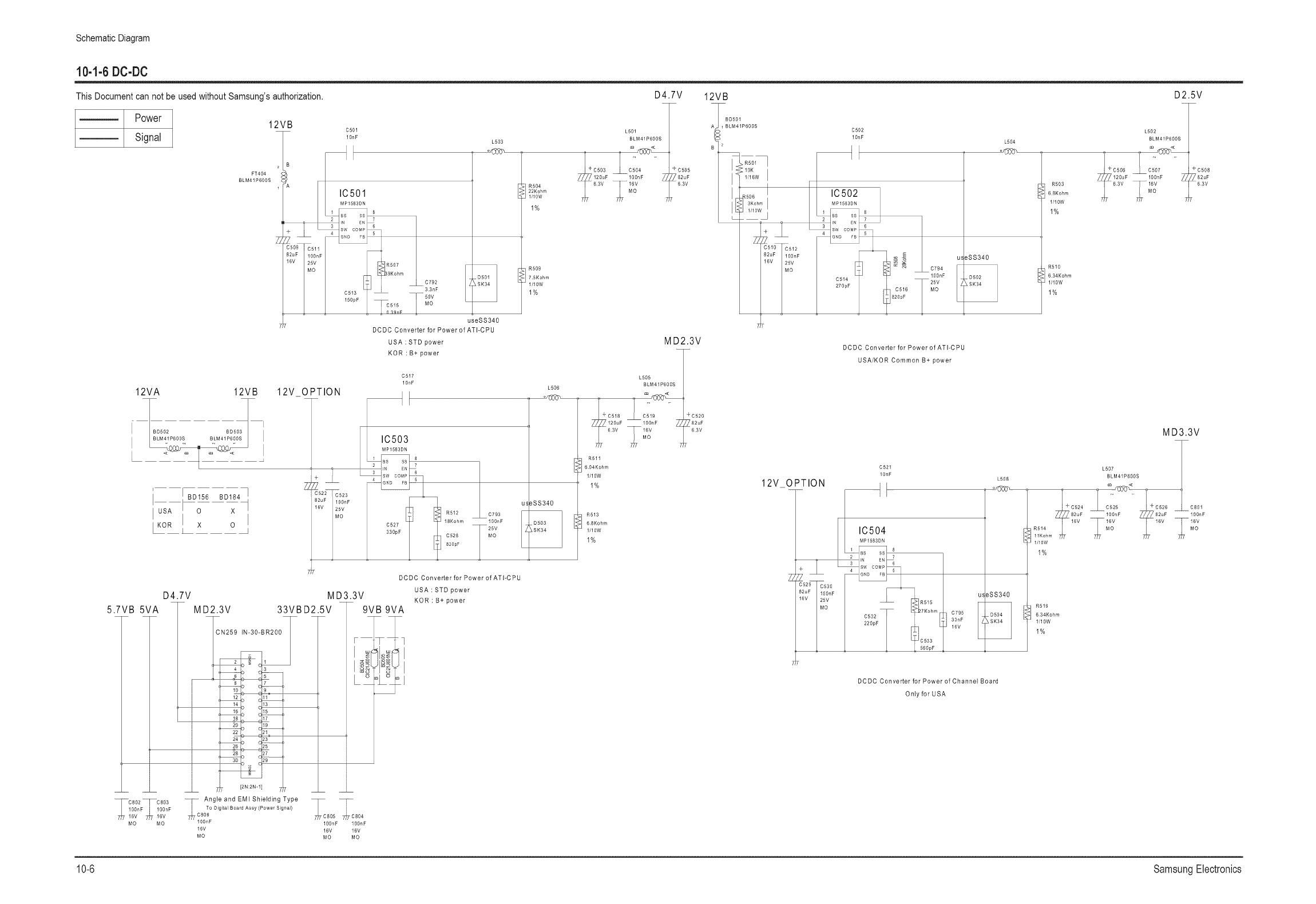
Schematic Diagram
10-1-6 DC-DC
This Document can not be used without Samsung's authorization.
Power
Signal
12VB
FT404 T
BLM41P600S
1
12VA
i BD156 BD184 1
I USA O X
KOR L X O J
12VB 12V_OPTION
2_
522_ 523
!uF lOOnF
}V 25V
O
C501
lOnF
L503
IC501
MP1583DN
1 8
2 7
R507
9Kohm
C513
15gpF C515
'tgnF
D501
C792
..........33nF
...................50V
NO
useSS340
DCDC Converter for Power of ATI-CPU
USA : STD power
KOR :B+power
D4.7V
R504
22Kohm
1/10W
1%
L501
BLM41P600S
+C503 _C504 _C505
_ 82uF
63V
R509
7 5Kohm
1/10W
1%
C517
10nF
R512
18Kohm
C528
820pF
lOOnF
L506
_SS340
MD2.3V
L505
BLM41P600S
+C520
_82uF
63V
R511
6 04Kohm
1/10W
1%
i R513
6 8Kohm
1/10W
1%
12VB
D4.7V
5.7VB 5VA
-- "C802 _
100nF
16V
NO NO
DCDC ConverterforPowerofATI-CPU
MD3.3V
MD2.3V 33VBD2.5V
CN259 IN-30-BR200 1 F
2
4 = 3
10 9 '
12 11
14 13
16 15
18 17
20 19
22 21 ' =
24 23 =
__ [2N:2N-1] f _ __ __
_c AngleandEMIShieldingType _c _c
To Digital Board Assy (Power Signal)
806
7_T [100n F 805 804
lOOnF lOOnF
16V
NO
9VB 9VA
USA : STD power
KOR:B+power
C502
lOnF L504
F
.... C516
820pF
aSS340
DCDC Converter for Power of ATI-CPU
USA/KOR Common B+power
12V_OPTION
C521
lOnF
IC504
MP1583DN
2 7
e515
7Kohm
C532
1 t i'0533
560pF
L508
u: _SS340 |
33nF
16V
DCDC Converter for Power of Channel Board
Only for USA
D2.5V
R503
6 8Kohm
1/10W
1%
L502
BLM41P600S
+C506 _C507 + C508
_82uF
63V
R510
6 34Kohm
1/10W
1%
MD3.3V
Z_ 524
82uF
16V
R514
11Kohm
t/t0W
1%
R516
6 34Kohm
1/10W
1%
L507
BLM41P600S
16V 16V
MO
C801
----100nF
--16V
MO
10-6 SamsungElectronics
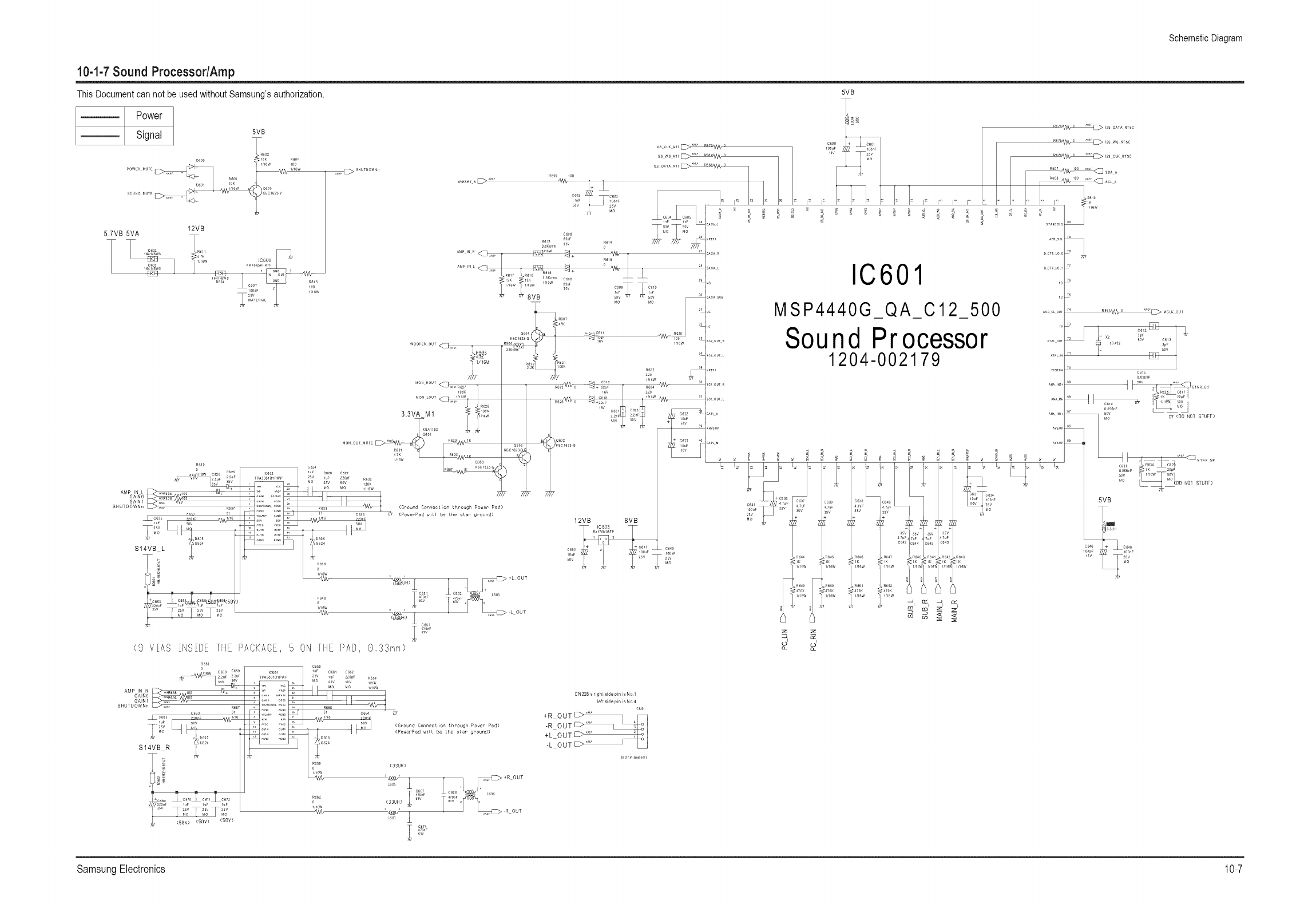
Schematic Diagram
10-1-7 Sound Processor/Amp
This Document can not be used without Samsung's authorization.
Power
Signal 5VB
_[11R_2 R_4
12VB
5.7VB 5VA
.... _611
C_3
AMP N L _,, ,
GAIN1
SHUTDOWNn
_c_s5
2SV
NO
S14VB L
_,_ _ SHUTDOWNn
nRESETS_ _*_
C_
22_
R_12 R_14
' ' SSV C_ C_1_
.... .......in<<1i_wi,
1/15g R_ _ R_21
l_SCLK ATI_v n
I:::! o
...._--q+ 21° _o_1'1°_
L4
12VB 8VB
s_v _sv
MO
5VB
IC601
R_74/V_¢ # .... _ 12S DATA NTSC
.c
MSP4440G_QA_C 12_500
Sound Processor
1204-002179
z
(D I
z
o
-11 Q21
C631 C634
1oa_ 1oon_
_OV 25V
__, z_,
AUDCLOUT
Z_
×TALI.
Z_Z_.
A.AI._,
A.AI.
A.AI..
_WU_
_WU_
b
71
_@_ ,,_ out
sp_
x_ _v c_i_
c_i_
I STNRSI_
5%V
c_i_ _ i/i_w _v
Z)/ (DC NO] SUFF)
c_s_
_v
MO
5VB
R_S
AMP N R ,*_R_55 100
GAIN1
SHUTDOWNn
T_v I
S14VB R
4/V91,1_
c_
ic_4 i_ c_1 c_
TPAS_IDIPWP _V I_ _p_ R_4
, ,_ MO _V _V I_K
M_ MO I/1_W
g _r
"o _ (Po_erPad _ll be the sler ground)
, (33[,,')
.... ;S _F T_S_F[_
_,16W ¢33U_O '
]
_F
CN228 sright side pin isNol
left side pin is N04
CN_
+R OUT .....
-R OUT
+L OUT
-L-OUT
SamsungElectronics 10-7
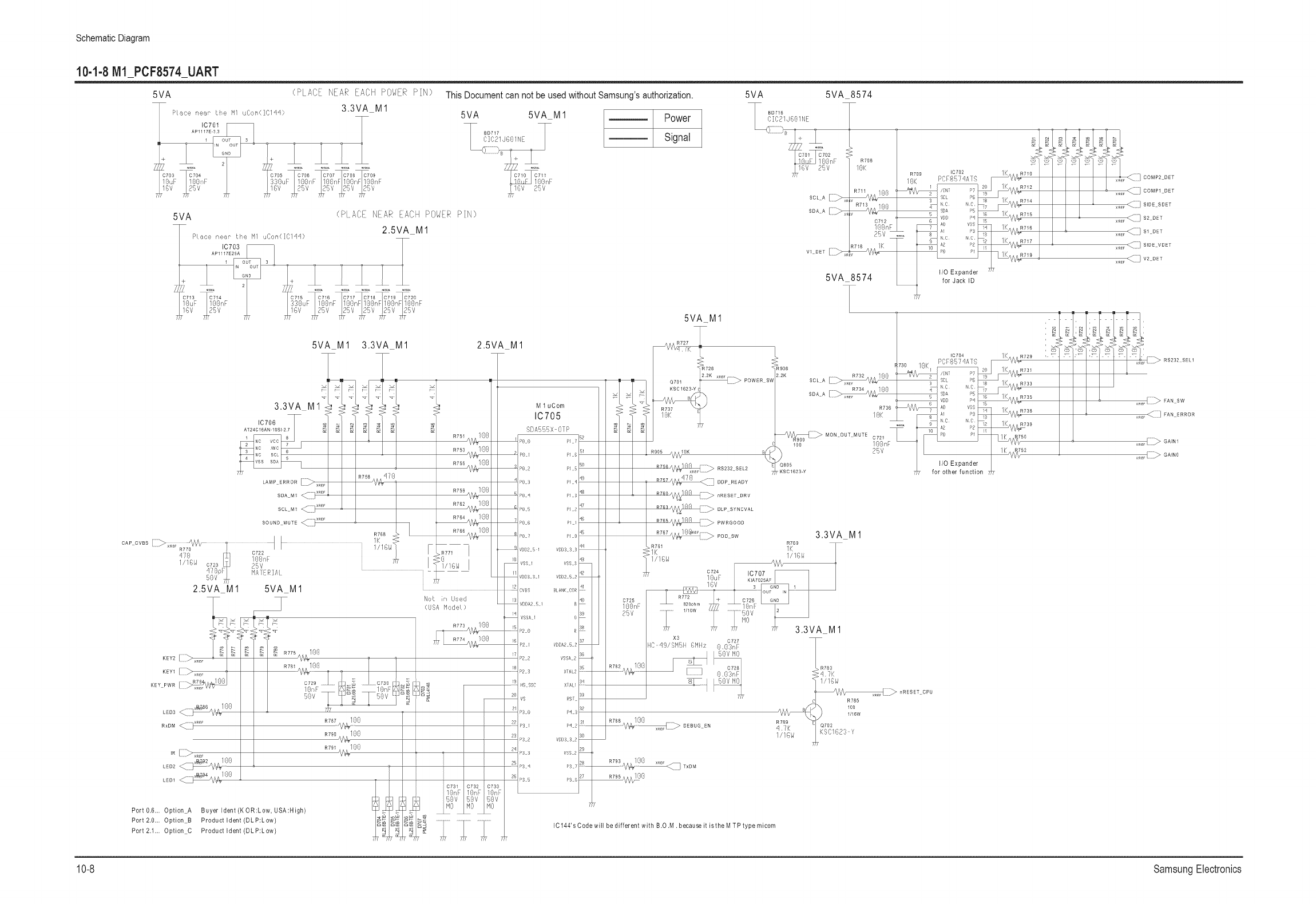
Schematic Diagram
10-1-8 MI_PC F8574_UART
5VA
PLace near' Lhe N uCom(iC1 )
IC70t
5VA
PLace near" the H1 uCon(]0144)
IC703
(PLACE NEAREACHPOWERPIN)
3.3VA M1
ThisDocumentcan notbe usedwithoutSamsung'sauthorization.
5VA 5VA M 1 Power
Signal
I08n
25V
5VA 5VA 8574
BD716
CIC21JG81NE
Z
O701 0702
_08DI R708
"6V _SV OK '
R709 10702 i K,_ /,^ R71S
10K PCF8574ATS _VW
SCLA [ > _11/_,,_ 08 _'V'_"__VV2R714
...... R713 • e _ C NC ,
...... VDD pq 6 K R715
O712 6 A V
....... R718 /K / _ _ VV_-
/I/O Expander "_
5VA 8574 / for Jack ID
< ooMn_D_T
COMP1 DET
= SIDE SDET
.... $2 DET
/.....
XRE_ $1 DET
XRE_ SIDE VDET
.... V2 DET
188nF
25V
777
5VA M1 3.3VA M1
SOUND MUTE _ ] .... 7
R768 I
...... s[>_ _vW I _ _ K
z_7;¢_ C722 1/16W >R771
u_q HA ER]q _ H
58v _ ..... T _2
2.5VA M1 5VA M1 ioi ilis_
• d Is
7 _ ( SA ModeL)
:_ ,_£,,_::__ _ ,_ _ .......
;. ..../ .....',_80 l ] ,_
...... .... doo !/
......... v v
Port0.6... Option A Buyerldent(KOR:Low, USA:High) l_ _ _ _
Port 2.0... Option B Product Ident (DLP:Low) I_ I_ I_ ......./..............I...............I ........
Port 2.f... Option C Pr oduct ,dent (DL P:L ow) _ _T_ _T_ _ _ T_ _ _ T_
2.5VA M1
I
_P8_
P8
4p83
_p(}q
P85
P8 6
PO Z
VD92 S I
YSS 1
VOD3 3 I
CVBS
VDDA2 5
VSSA I
P2 S
P2
P2 2
1>2 3
HS %8
YS
P3 @
3
P3 2
P3 3
P3 '1
P3 5
M 1 uCom
IC705
SDA555X 8TP
PO e
5VA_M1
>
_728
22K XRE_
_0cI,..... ......sv
•.... , B
R905 A_Vl OK 8{(
_7_ _s_ s_
_ R757 /\_A_]]]] DDP READY
_7_> _W_OOD
R767 / ()_RE_ ....... _ODSW 3.3VA M1
• R761 R769
:11_ 6W 1/16W
I LJI K:AT025AF
c725 R7_Z.... _ C726 GND
25V188n ................_ _I))v VA M1
X3 C727
IC qS/S 5 6MHz () ,83nF
C
R788 I08
.... D_u__N
_908 730
22K •
....... R734 ,,, /00
SDA A
R736 _y\
/ 8K
_ss I80F
25V
Q805
KSC 1623-Y
_\A/_}}}_ nRESET CPU
R785
100
1/16W
Q702
_8C1623 Y
4I7 K
1//6W
IC f44's Code will be different with B.O .M. because it is the M TP type micom
'j Q
10704 iK^ _, _ R729 , L
,PCFS574ATS r_Vv_
__vw
6VDD Pq
N C NO _ 112 _*-- R739
18 A2 P2
I/O Expander
for other function 7)7
ii_ Rs232SEL_
FANSW
.... _N _o_
I....
XRE_ _ GAIN1
XRE_ _ GAINS
10-8 SamsungElectronics

Schematic Diagram
10-1-9 Signal Connection
This Document can not be used without Samsung's authorization.
Power
Signal
R923
_47K
R917
OSUBTXO_ .... _!V
GT1 8VA FAN
BD712
ClC21JBO1NE
CN16 _ ....... C789
100nF
16V
MO
RS232 $EL2
1C714
M C74VHC244DTR2
................c;_ ................. 120
7ZT //
3.3VA M1
.........._a;1_/._BnE5v
_A_-_ FAN ERROR
1/16W
CableCARD Cooling FAN
5VA
(I2C l/Sf)
CN13 /
.............1 .... BB_t_
For Debugging
A _ C i
z
1.1R 1.5VA 1.GND 1.LED1
2. GND 2. KEY-PWR 2. KEY1 2. KEY1
3.5VA 3. GND 3. KEY2 3. KEY2
4. LED1 4. GND 4. SDA-M 1'
5. LED2 5. SCL-M 1,
6. LED3 6.5VB
7. GND
Used as follows...
L3 A+B,C
L5 A,B,C
L7 A,D
C810
33uF
25V
_8232 SELl
WV_'Z_ ........
_,_/_ DEBUG TXD
R920
5VA
ClC21JBO1NE
R910
_IK
/
\
R912
R911
/_/ 0
IC713
MC74VHC244DTR2
J
//_/c Nii?
?
i4
16
01
!5
I5
D2
1!__
I7
A
Front IR/LED PCB - IR
R811
1OK
1/16W
IR _XRE_
D802
CDSSCS0GT,
5VA
BD71_
CIC2
CN17 ................C775
IOOnF
CN18
LED2 ....... O
LED3
B
Front IR/LED PCB - LED
L
LED1 XREF
KEY1 _
KEY2 ...... R812 0
SDA M1 l_t3_SCLM1
L7 CABINET
'VW_AR¥ RSRXO
/VV_/ ANY RS TXD
R922
0
C
Side Key
12VB
BD709
CIC21JBO1NE
D
Front KEY/LED
C779
25V
25V
/T_ C781
IOOnF
25V
70VB 5VA 12VB
SOL M1 XREFSDA M1 _XREF
/
C77_F !
loon
........DEBUG RXD
........ _C
ANY RS RXD
OPTICAL OUT _XRE_
12S CLK NTSC _ XRE_
12S DATA NTSC
12S ws NTSC xR[_
12S CLK ATI _XREF
12S WSATI
3.3VA M 1
/T_ C783
IOOnF
//7 2_v
ANYNET TXD
ANYNET RXD
ANYNET TX
ANYNET RX
DSUB TXD
BSUB RXD
i _ 11:1
..........o
io!
33uE 1BBnF
25V 25V SMW200-12P
_MO CN260
From/To Sub-Detect PCB
CN20
FW20010-32
TxDM
XR[_ RxDM
xRE_DEBUG EN
XREF nRESE_ CPU
XRE_ nRESET DRV
XRE_ DLP SYNCVAL
SamsungElectronics 10-9

Schematic Diagram
10-2 Digital Board
10-2-1 Digital-I
This Document can not be used without Samsung's authorization.
Power
Signal
D5.7V
_C16!6
100nF
25V
MD:k3V D4.7V MD2.3V
100uF 100nF 100uF 100nF
16V 25V 16V 25V
_ _ C1609
100nF
25V
T
FT1201 , T
T-
FT1200 15
2T-
FT1203 25.......
BLM41 P600S 2:7-
(_)_ 29
BD1005
ClC21J601NE
777
CN17
IN-30-BR200
z
) C
) C
) C
) C
) C
) C
) C
C
z
FT400
2 <_ ca
FT!202
BLM41 P600S
FT1204
BLM41P600S
_@-o _<
ca
FT401
777
TU 33V D2.5V STB 5V MD9V
C16!4
100nF
50V
C16!2
47uF --100nF
16V 25V
C16t0
47uF 100nF
16V 25V
25V
RS232 TxDRS232RxD
_R1383
_!0K
i1/16W
ANYNET TxD
ANYNET RxD
SPDIF ATI _ R2_W_-0
....NT 12S DATA
NT 12S LRCLK
XREF R12 0
12SSCK OUTA
12SSD OUTA XREF R915 0
_swsOUTA_!
CN29
FW20010-32
3 oo
55 7
5_
5_
51
oo
o o .......
<_ (_
oo
-o0
oo
oo
oo
oo-
o o
-oo
00
@o
z
6
12
14
16
18
20
22
24
26
28
30
32
R3280 __
TxDM
RxDM
SDA
R599 SCL M5
nRESET SOUND
nRESET ANALOG
LAMP ERROR
DDP READY
POWERGOOD
_ MICOM INIT
nRESET
nRESET DRV
SYNCVAL
D5.7V
REG400
KIA78D05F
O136!
....................100nF
--25V
L402
CIC21J601NE
i l_u _
+ C!369 C!364
F 100nF
-L_25v
MATERIAL
A5V
BD1006 ....................
ClC21J601NE
C1472 ............ C156!
10uF 10nF D5V
16V T Mo50V iii 2
L407
CIC21J601NE
t C!424 0
10uF
16V
USB 5V
CN500
SMAW200-30C
2 1 XREF
O O MAIN Y
--O O 3 XREF MAIN C
5 XREF SUB Y
O O 7 XREF
18o --o o 9 xR_ SUB C
1_ o o ii _ COMm Y
22 _ O 2i COMP2 PR
--O 0 _ MTNR CVBS
--0 0 25 MTNR SIF
28 O O STNRCVBS
STNR SIF
--O O DTV CVBS 1
R391 R392 R390 R394 R395 R393
75 75 75 75 75 75
1/16W 1/16W 1/16W 1/16W 1/16W 1/16W
A5V
.... KsclQ_-01 ( _ti t_ ........... xR_[<_ DTV CVB S
DTV CVBS 1 <[[[} R327 1/16W _ R597
i; 0w
10-10 SamsungElectronics

10.2.2 Digital-2
This Document can not be used without Samsung's authorization. MDOV
Power _
Signal
TUI
DNVD3_BV401A
TUNER 1
.....I..............I.........
lo,,F loo,,F
OOB PLL3.3V
L611
C_C21J601NE
0::)B
STB 5V
L613
MPZ2012S300A
LC689 Z_
LC6_F0 ...... C2u57
T _T T _'_ 16V
TU2
I
I
I
TSI ERR
] TU nRESET 1
> ETX
MD3.3V
TUIS I
csol + cso2
......IO,,F I_F
> _ S0V S0V
_B
M AFT
R534 0_
R535 100 _ TU nRESET 1
R1017 _ 100 TS_ ERR
......
RS41 _ 100 XTALON OFF 1
MTNRS_F
RS43 0 DRX
TU 33V
hSOO _ ........
C_C21J601NE
ALPSN_MTUNER
SEC N_MTUNER
IOOB_PLL3.3V
L211 I
C_C21J601NE
R_40 0 CRX
LS02
C_C21J601NE
MD3.3V
CH1.25V 1
CH1.8V 1
I ...... ]
C_C21J601NE
/CH2 5V
SEC POD TUNER
SEC N_MTUNER 1
LS01
C_C21J601NE
_cslo
loo,,F
STB5V
L1001
ClC21J_OINE
STB 5V
STB5V OOB PLL3.3V
_C67_
_ .....
MD3.3V
NEW ITEM
CH2.5V 1
MD3.3V
I?£,F
SECPOD_NER
SECNIMTUNER
.... ,,E_ ITEM
CH1.8V1
MD2.3V
IC_F
NEW ITEM
SC1566
CH1.25V1
GEM 5V TOGEMSTARSheet9
CiC21 JOOINE J
POD 5V
BDIO_I
ClC21J_OINE
Schematic Diagram
SamsungElectronics 10-11

Schematic Diagram
10-2-3 Digital-3
i CH3.3V 2
Power
Signal
TUNER 2
ALPS NIM TUNER
TU500
::;i2:iii?
xi::i?i
DELETE
777
L507
CIC213601NE
_ C53! __ C532
10nF 100nF
ANALOG TU 5V
SUB TUNER AGC
[]]_ S AFT
R560 100 TU nRESET 2
R__ __ TS_ERR
S CVBS T
R_ XTALO_ OFF2
STNRS_F
R557 100 TS2 SYNC
R556 _1 TS2VLD
TS2 DD7
TS2 DD6
_' TS2 DD5
TS2 DD4
TS2 DD3
TS2 DD2
_' TS2 DD1
TS2 DD0
R563 TS2 CLK
R590 SDA CH2
R591 SCLCH2
/ L _" "_SDA SUB NIM
/ ] _SCL SUB NIM
L_
iC537 i C538
10nF 100nF
CH1.25V 2
S TU 5V
L504
CIC213601NE
ANALOG TU 33V TU 33V
.......... C523
10nF
+ C524
_ luF
50V
L505
CIC21J601NE
ALPS NIM TUNER CH1.8V 2
i
BD50!
CIC21J601NE
SEC NIM TUNER
, L_0_ CH2.5V_2
CLC21J601NE
i
L
LC543 __ C542
10nF !00nF
DELETE
SOVBST IRIII
<_> 75 16V
1/16W
S TU 5V
10K
1/16W
R580
__'_//Q500
KSC1623-G
_R576
@0
_>I/16W
e _x#_TNR CVBS
_R578
C-P'_K
1/16W
D5.7V
BD500 1C506
CIC213601NE KIA78D05F
C520
100nF
25V
MATERIAL
S TU 5V
=
+ C512 C514
25V
MATERIAL
[Sub Tuner]
D4.7V REG_0_
APll17E25A
1 ..................IN_c_33 IN iO
100nF
25V
MO
DELETE CH2.5V 2
l+ C534 C535
ZI 11_Ou_ i_On F
D2.5V
- IC513
G953-t8T6U
C539 1 _N_GG
100nF
25V
MATERIAL
DELETE
CH1.8V 2
C536
100nF
25V
MATERIAL
DELETE
D4.7V
BD1004 IC1208
010211601N E AP1117E-3.3 .........3L
CH3.3V 2
I c_0_° c_0_F_
_ovT _ERIAL
D2.5V
-- -- REGS02
RT9183-12
1 IN Oi
__ C546
100nF
-- 25V
MO
DELETE
L509
T 3 010213601NE
C551
100uF ..... 100nF
10V 25V
___5_ VS_F
CH1.25V 2
_
04
OU)
LO a.
ANALOG TU 5V
o(D
o_
CIX
A/W 1
ANALOG TU 33V
%
X_
SUB TUNER AGC
R595 100 1/16W
_ SCL CH_
.vSDA CH_
89 1001,16W
L_ STNR SIF
S AFT
IJ_ {]][])> S CVBS T
10-12 SamsungElectronics
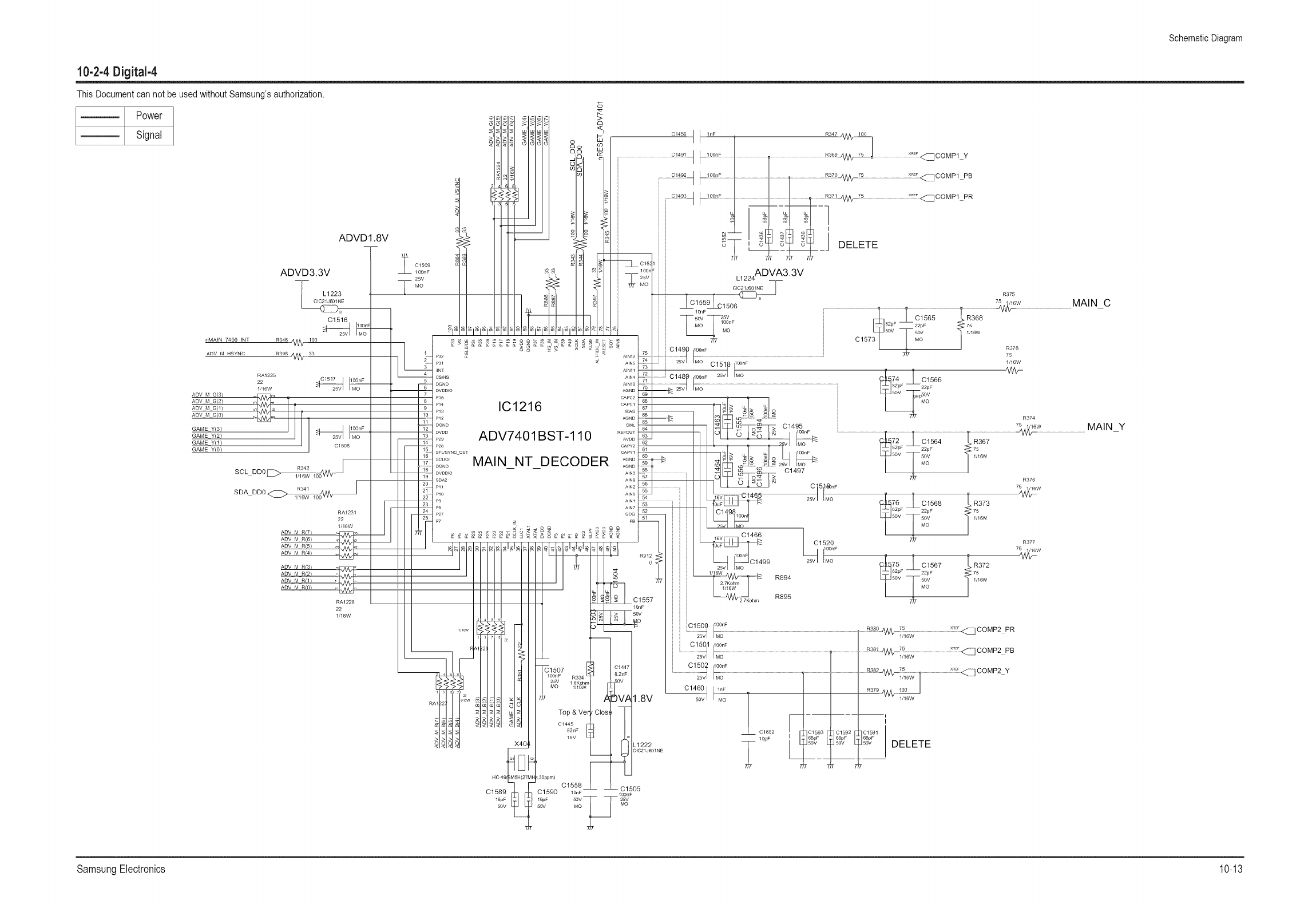
Schematic Diagram
10-2-4 Digital-4
This Document can not be used without Samsung's authorization.
Power
Signal
nMAtN 7400 INT
ADV M HSYNC
ADVD3.3V
L1223?
C1516
ADVD1.8V
c1509
10on F
R346 _ 100
R398 _ 33
RA1225
100nF
22
1/16W
ADV M, G(2)
ADV M, G(1 )
ADV M G(0)
GAME Y(3) _ poonF
GAME Y(2) MO
GAME Y(1) C1508
GAME Y(O)
8
___ .... _g° ,o ................................................_,4______0F
_" _ .......... C!!9_ 100nF ...............................................................................[ _ R_9--/W_/--_--_R370JW_'75...............................{_[ <:_QOMP1.... QOMP1 YPS
_!4_34 F !qpx![ .............. I ....... I _ :B_[(!-!W_7_ ......................................... _F_:<::_]OOMP1 PR
_ _ /
i
I_ !_1_ _ 8 8_ J DELETE
-
loon_F ADVA3.3V
_-25v/ L1224
_M°/ o,c........T
f '_ _" _ R375
/[01559 [r1506 75,1/_6w MA N C
8_ /i -_°nF_TSovT25v ............................................._J_ f.................._ C1565................................................LR368f................................VVV- ..................................................
I$151 _>_ _ $1_!# <_ _, I _o soy Tsov ew
/ 7/7 015731 / _° /
......... 4................. _ _ ........................................................................................................................ 7}7 7_
P31 AiN5 25Vl IMO PIKIR _100nF 1/16W
/'c_:,s ^2_//4 0148_ I_OO_F_:F ]MO &74 101566
_v_o ^"£ _2_vq F_o............................................................................................................................i?]_: __ ....
P15 CAPC2 69 _0v ap50 v
"'_ IC1216 ..... 00; _o
P13 BIAS 66 O
P12 _iii _ _a{ R374
.... C1495 ............................................................................................................................................................_6w ........................................MAI N_Y
_v_oo ADV7401BST-1 10 "02 _ _72 TC1564 _R367
.......... sov s£ .....
SCL DDO_
SDA DDO_
RA1231
22
1/16W
ADV M R(7)
ADV M R(6)
ADV M R(5)
ADV M R(4}
ADV M R(3) _[_
ADV M R/2}
ADV M R/1}
ADV M R/0_
RA1228
22
1/16W
CAPY2
CAPY1
..... MAIN NT DECODER ....
DGND -- -- AGND
DVDD]O AIN3
SDA2 AIN9
Pll AIN2
AINBplo
P9 AIN1
PB AIN7
P27 SOG
P7 18 _ _ 0 0 _ O0 O0 0 0
25V 16Kohm
MO 1/10W
Top & Ver
C1445
82nF
16V
61
5B
TF ................................
%6
54
g2......................
5_
5_
R912
0
1.8V
L1222
C1021J601NE
C1497
7_T R376
_ 5,t_)nF 7_6 W
25VIIMO 76pF&o1568 ov/ R373.....
C152OF 7_T 7_ W
01499 25_v ]MO _75 &01567 _R372
1/16W 82pF 22pF
R894 5ov Tsov /1/16W
MO
R895 7_T
_: ................................................................................................................................f_#__V_fJ _............................................x_E_-_ COMP2 PR
25W " -- 1/16W --
C!:v_ 1 _-_2nF.............................................................................................[ ............................._&#!JW_-_f_6 W.................................._[<::_ CO MP2 P B
_v,_o.......................................................................].............................................................................._ co_ Y
_ C1602 i V_C1593 I_1C1592 FC1591
C1558
C1589 C1590 _O_F C1505
50V 50V MO MO
SamsungElectronics10-13

Schematic Diagram
D2.5V
01539
100nF
= 25v
MO
NEW ITEM
IC1223
G953-18T6U
3
_ OUT
G_D .....
2 100UF 100nF
10V 25V
MO
ADVD1.8V
i
D4.7V ADVD3.3V BUF D3.3V
BD1009
ClC21J601NE
IC1209
AP111_E-33
....... u 0145! 01541
--100nF
--25V
MATERIAL
',DNIE 3.3V TO DNIE Sheet15 ,
'_ '
BD1017 , ....................... ,
CIC21J601NE
D4.7V ADVA3.3V
ClC21J601NE C1210
AP _E-3 3
_oo +C::u_:%
10-14 SamsungElectronics
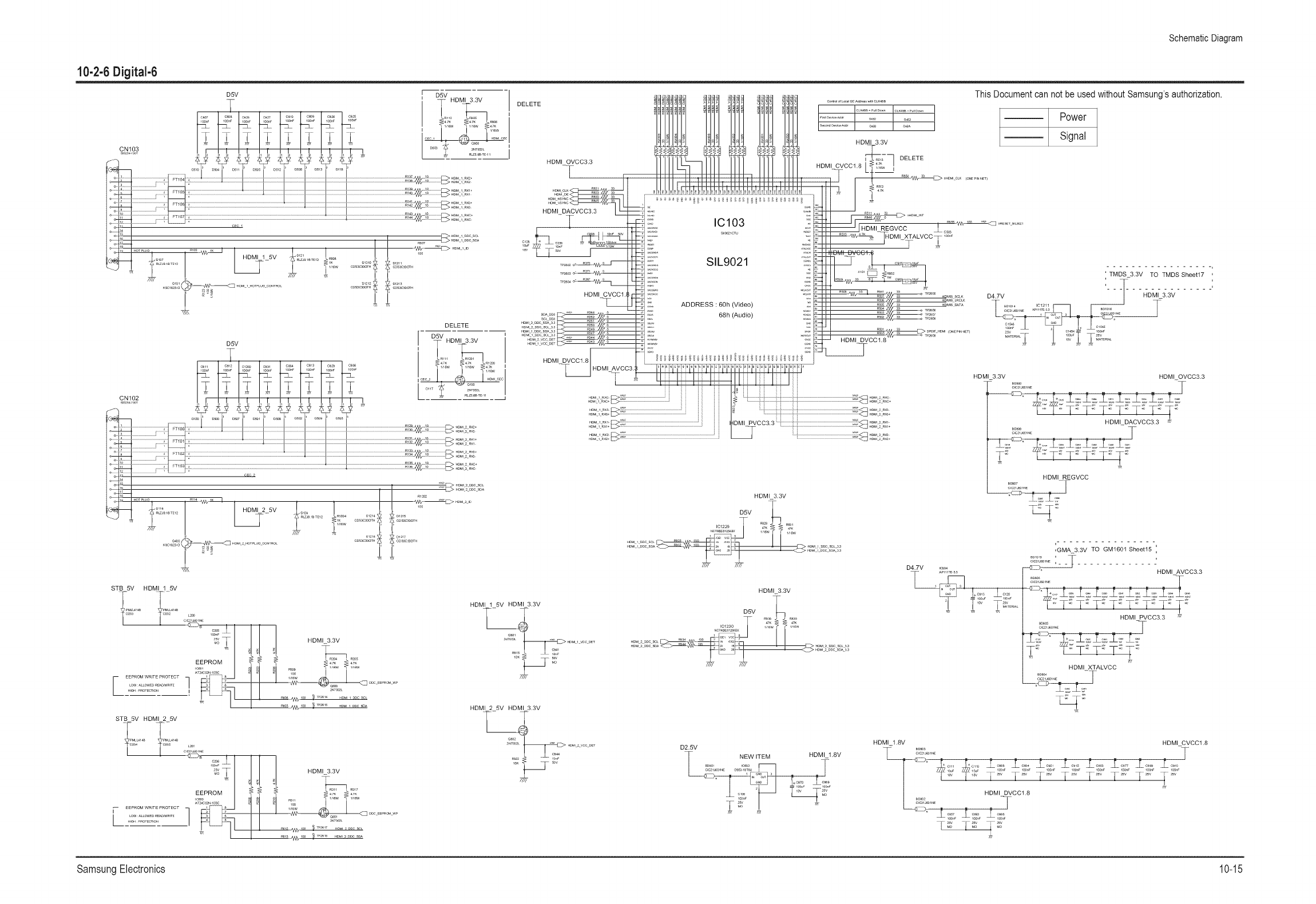
Schematic Diagram
10-2-6 Digital-6
D_V [ D_V I
_ HDMI 3 3V I
l = " I
o
o_
o_
DELETE
DELETE ®1®1®1®1i i
HDMI OVCC3.3
HDMI DACVCC3.3
HDMI CVCCl.,
HDMI DVCC1.8
IC103 ::
":%
SIL9021 _!:_i:!
c
ADDRESS : 60h (Video)
68h (Audio) ::::_:
c:
;ot__,':_:: ....................................................................
HDMI 3.3V
HDMI 3.3V
DELETE
HDMI CVCCl.8 _,_w I
This Document can not be used without Samsung's authorization.
Power
Signal
x1_1_
H_MISSClK
HbMISpATA
HDMI DVCC1.8
D4.7V
' TMDS 3.3V TO TMDS Sheet17 '
-t: HDMI 3.3V
HDMI 3.3V HDMI OVCC3.3
HDMI DACVCC33
HDMI REGVCC
STB 5V HDMI 1 5V
EEPROM
STB 5V HDMI 2 5V
....t t:....
HDMI 3.3V
._o_ ___t, .... . ..........
it t HDMI 3.3V
HDMI 1 5V HDMI 3.3V
_,_::_ ...........
HDMI 2 5V HDMI 3.3V
F
_i_i_ ..........
HDMI 3.3V
D2.5V
NEW ITEM HDMI_1.8V
D4.7V
HDMI_1.8V
I
,GMA 3.3V TO GM1601 Sheet15
HDMI AVCC3.3
T_ .....
HDMI PVCC3.3 Ill
HDMI XTALVCC
HDMI CVCC1.8
T
SamsungElectronics10-15
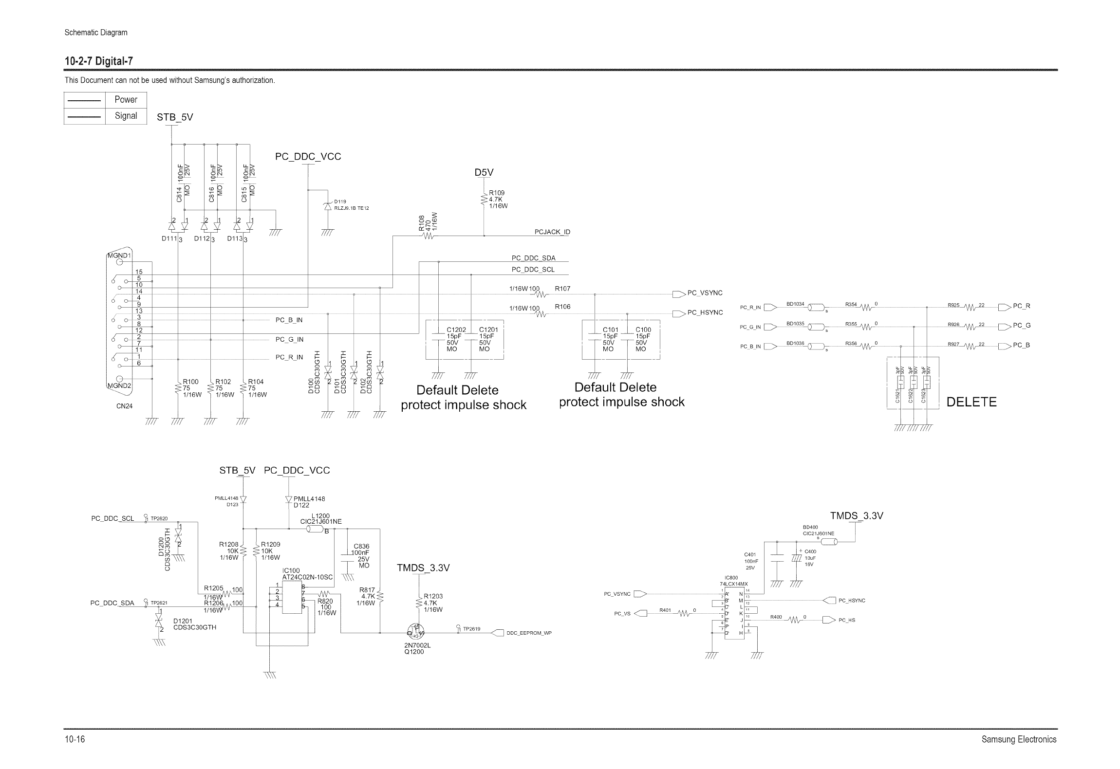
Schematic Diagram
10-2-7 Digital-7
This Document can not be used without Samsung's authorization.
Power
Signal STB 5V
I..........................
3
!3
PC DDC VCC
Dl19
RLZJ9.1B TEl2
D5V
LRlOO
_4.ZK
_1 1/16W PC JACK ID
PC DDC SDA
Default Delete
protect impulse shock
Default Delete
protect impulse shock
BD1034 R354 0 R£25_/_,/-_ _ PC R
BD1035 R355 0 _ PC G
PcGIN_ ......... • _W.......
BD1036 R356 0
_> u.> u.
© ©
//T77_
PC DDC SCL
PC DDC SDA
STB 5V
PMLL4148
D123
_ TP2620
N°o R1208
10K_
1/16W
R1205 10C
_:_ TP2621 _'_VV _
R1206AA1/_0C0C
2 1/16Wvv
D1201
CDS3C30GTH
PC DDC VCC
- .1414
1:)122 1_1200
_R1209 C836
"_> 1171_W _010100 _ 2_OvF
_2_ \\\\ R817_
1/16W I
TMDS 3.3V
TR1203
_4.ZK
/_l_, 1/16W
_J
2N7002L
Q1200
_1 TP2619 _ DDC EEPROM WP
TMDS 3.3V
BD400 I_
CLC21J601NE
I °czb
;c oo OuF
100nF ......................... 16V
25V
IC800
74LCX14MX
PcvsYNcC::> _ _ Pc.sYNc
PC VS _ R401 4 b" K l !) _
R4oo__A/WoCD>Pc.s
10-16 SamsungElectronics
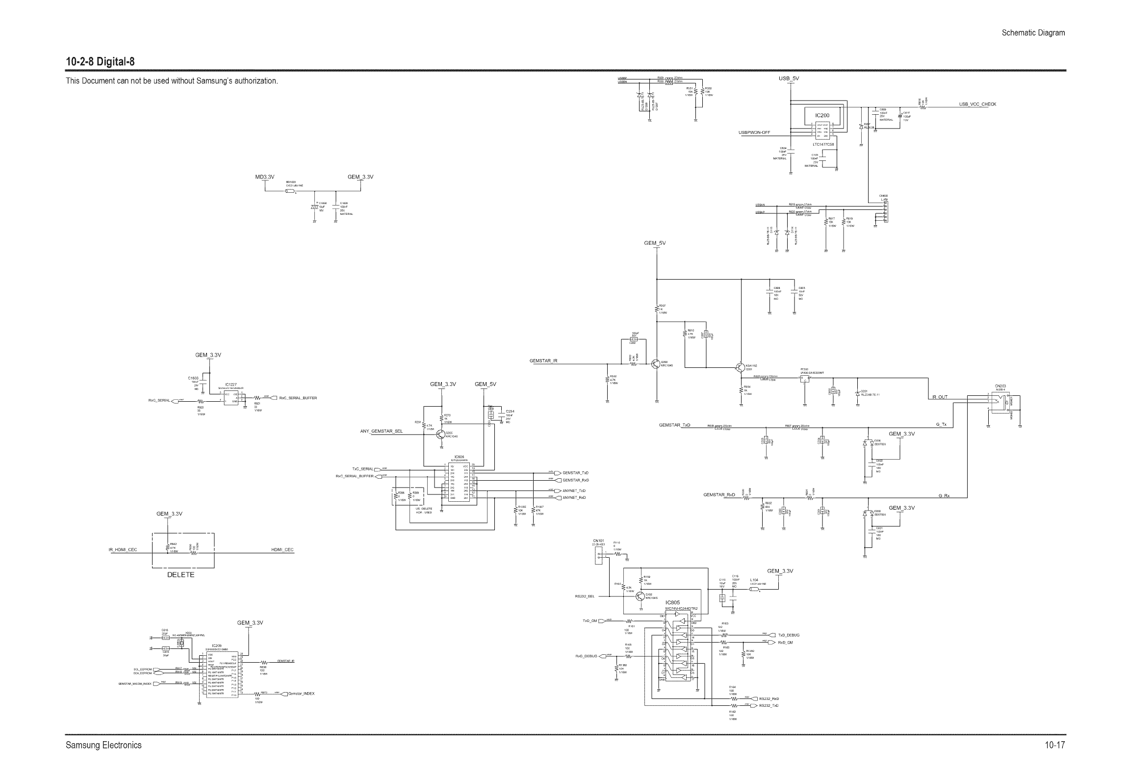
Schematic Diagram
10-2-8 Digital-8
This Document can not be used without Samsung's authorization. us_
_ I,..... I_w
USB 5V
MD3.3V GEM 3.3V
T
GEM 5V
LTC147 0S8
c_®
_sp
_ 2 USB vcc CHECK
GEM 3.3V
1,1_w
I
IR HDMI CEC
GEM_3.3V
DELETE
]
I HDMI CEC
J
GEM_3.3V
GEM5V
GEMSTAR IR
lR_o2
_GEMSTAR TxD
_a,_GEMSTA R RxD
_'_ANYNET TxD
_'_ANYNET RxD GEMSTAR RxD _-: _o_
4,'W_
i
CN101
1 I'1_w
GEM 3.3V
_ RS232 TxD
1,1_w
0N203
IR OUT
G Tx
3.3V
G Rx
3.3V
SamsungElectronics10-17
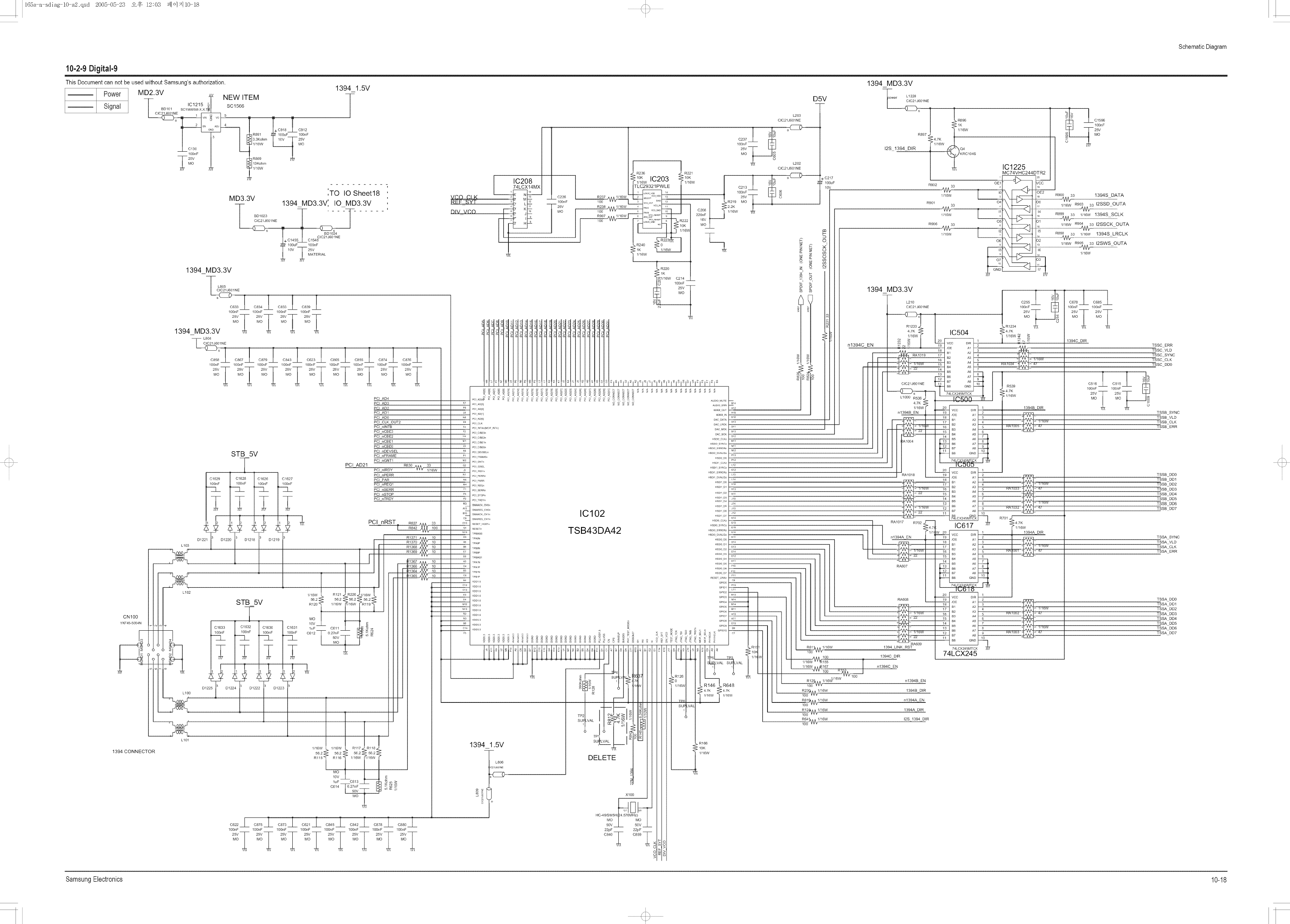
165a-n-sdisg-10-s2.qxd 2005-05-23 o_ 12:03 qlol_l10-18
i
...............................t............................... 1
Schematic Diagram
2 r
10-2-9 Digital-9
This Document can not be used without Samsung's authorization.
NEW ITEM
SC1566
vo 5 _1 l+ 1
_ c91_c912
li!°o_m_°o°v_£v_
R889 7_
1394 t.5V
MD2.3V
_[ IC1215
BDI01 SC1566t5M-X X T
CIC21J60tNE 1 vfN
100nF
MD3.3V
Power
Signal
25V
MO 13Kohm
1/10W
',TO IO Sheet18
1394_MD3.3V', IO_MD3.3V ,
T BD1023
CIC21J601NE ]
BD1024
C154 CIC21J601NE
100uF 100nF
10V 25V
1394 MD3.3V
L805
CIC21J601NE
100nF 100nF 100nF 100nF
1394 MDS.SV _T _T _T _T
L804
CIC21J601NE L222 _22 2
C867 C879 C843 C623 C865 C855 C874 C876
100nF 100nF 100nF 100nF 100nF 100nF 100nF 100nF 100nF
STB 5V
CN100
YKF45-5004N
_j O(
)
L103 Dt221 I D1220 [3
L
Lt02
J
D1225
L101
PCI AD21
Ct627
STB 5V
p
i
i
[i
1/16w R121 _ R226
56.2 _ 56.2 : _ 56.2
R120 _ 1/16W :_/16W
1
MO
C1633 Ct63_ Ct631 110iV-- C611
TT__ c_T°_7_-T
D12 31222 I D1223
PCI AD4
PCI AD3
PCI AD2
PCLAD1
PCI ADO
PCI CLK OUT2
PCLnlNTB
PCLnCBE3
PCLnCBE2
PCLnCBE1
PCI nCBE0
PCI nDEVSEL
PCI nFRAME
PCI nGNTt
PCI nlRDY
PCI nPERR
PCI PAR
PCLnREQt
PCI nSERR
PCI nSTOP
PCI nTRDY
PCl nRST
R830
Rt371
Rt370
Rt368
R1369
1394 CONN ECTOR 1/16W
56.2 <<
Rl15 <
56.2
MO
10V E
luF C613 _ _
C614 _ _
MO
C622 2 C875 2 C873 _ C621 2 C845 2 C842_ C878 2 C880_
100nF 100nF 100nF 100nF 100nF 100nF 100nF 100nF
_vT_vT_vT_vT_vT_vT_vT_vT
D5V
L203
CIC21J601NE
IC208
I 74LCX14MX
V_O ___ _
REFRBYT 2L TL_
D,v vco _ i_
R236 R22t
_d0K £
;/°_w IC203 >_/_6w 02_3
I ITLC29321 PWLE T
C226 R237 1/16W 13 25V
-- 100nF 100 s 12 -- R219 MO
--25V R238 1/16W 4 11 -- 2.2K
MO 100 1/16W
_oo7_,_ow _o_o_,,
_00 0 _0_222_vZ---_OT2
i i i i i i
220
1K
1/16W C214
100nF-- --
_lS!61sl_!_!_!_pp!_!_l_l_lSlSlSlS!2!_lLl_la
614
CIC21J601NE
_ O
ccI cc I
.C217
100uF
10V
p_
g
o
O3
o4
1394 MD3.3V
..... _10_221_6o_N_
_002 o_\ _voo
1/16w [ ,o OS2 Rg00 S3 1394S DATA
33 4 _,,I 17 1/16W R903 33 12SSD OUTA
-- _ f H \_II_ F_ _ ......
1/16W | 5 \ I _-..--2_ _6 R899 33 WS6W 1394S SCLK
| _l _...... dVV_ .........................
_oo6.. o_ ,,,ow_oo4..,_ssc.OUTA
1/16W I '7 \ ] _-_---4 _ R898 33 1/16W 1394S LRCLK
o6\'I%> ...........I-8_
B \ _ I _s ws6w R905 33 12SWS OUTA
r--_d---qt_ _ _ ......
1394_MD3 3V , £
T_o c__L
_I jCIC21J601NEs _ 25VR1234100nF_MO O
4.7K 4.7K
I _ _ I I_o_ _ / _
n1394CEN I 2_ _ 1 _ vc3 _ L= _^^
18 B1 A2 3 r_
RAt019 17 4 "°
B2 A3 5 _ ,_ W_6VV
B3 A4 6 HA1 U34 _ 'o 4/
B6 A7
B7 A8
B8 GND R539
1/16W74LCX245MTCX
/ ......
RAt018 _
" " _ 17 4 --_ _ I/TbVV
..........vv4.................
"_VL_ t7B48LCX245M_'_ I----1 R701 <_
- - _ RA1017 R702 _--- It"_17 7}7 _4.7K
4.7 [ P.._v_ t 1/16W
- 1/1 W 20 1 1394A DIR
! we
zz i15 s4 A5 6
iil:i 13 ....B5 A6 8 _ ,o 1/_6VV
1394 LINK RST 74LCX245MTCX_
11
C678 C685
100nF 100nF
_vT_v._
1394C DIR
100nF 100nF
_v_ 2_vPC[ ADI3]
PC[ AD[2]
PC[ AD[I]
IC102
TSB43DA42
37
w
1394 1.5V
DELETE
MO
50V
22pF I
C840 f
R81 t/16W 74LCX245
_w 7505_ 139400,_
1/16W 167 n1394C EN
_100 N_
Rt2_AA1/16v_/16w n1394B EN
R23 1/16W 1394B DIR
100 (_'W_/
R81 1/16w n1394A EN
Rt2 1/16W 1394A DIR
I O0 a/_A/
R64 1/t6W 12S 1394 DIR
1001/W_ - _
TSSC ERR
TSSC VLD
TSSC SYNC
TSSC CLK
TSSC DD9
TSSBSYNC
TSSB VLD
TSSBCLK
TSSB ERR
TSSBDD0
TSSBDD1
TSSBDD2
TSSBDD3
TSSBDD4
TSSBDD5
TSSBDD6
TSSB DD7
TSSA SYNC
TSSA VLD
TSSA CLK
TSSA ERR
TSSADD9
TSSADD1
TSSA DD2
TSSA DD3
TSSA DD4
TSSA DD5
TSSA DD6
TSSA DD7
SamsungElectronics 10-18
i
'\ $#
i
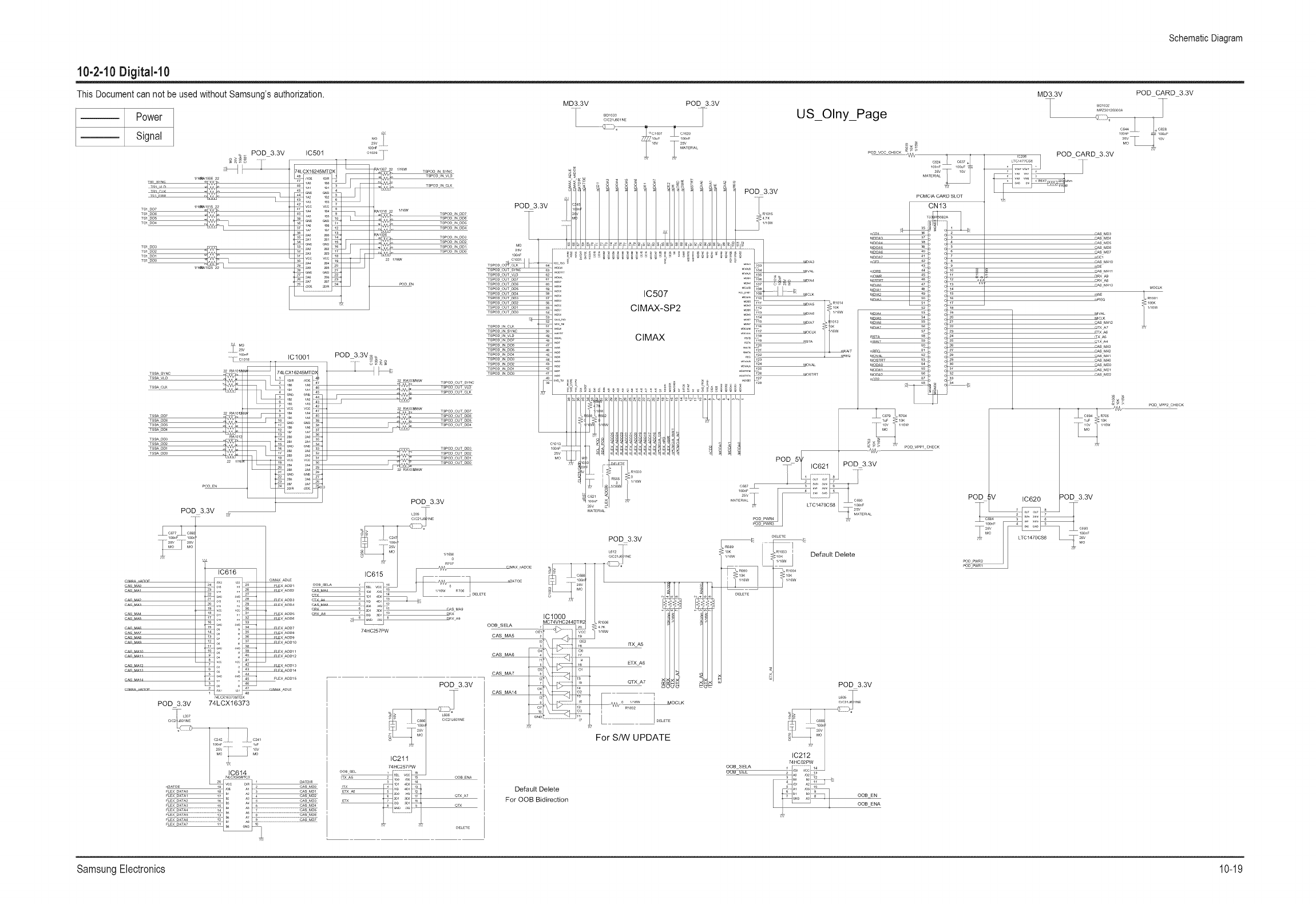
Schematic Diagram
10-2-10 Digital-10
This Document can not be used without Samsung's authorization.
Power
Signal
MD3.3V
BD1033
ClC21J601NE
POD 3.3V
US_Olny_Page
PoD vcc CHECK_V_/-
MD3.3V POD CARD 3.3V
BDI032
MPZ2012S300A
MOCLK
SamsungElectronics 10-19
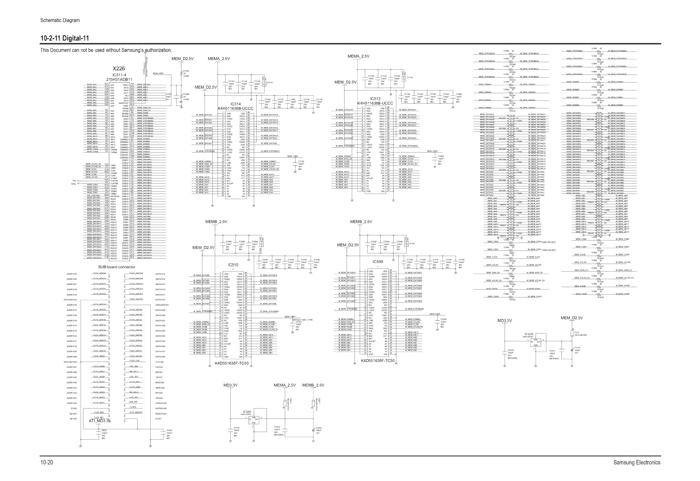
Schematic Diagram
10-2-11 DigitaM1
This Document can not be used without Samsung's _uthorization.
X226
IC51 1-4 MENVREF
215H31AGB1 1
M M AA8 _D D_ 27 _4 M _A_!
MM AAI A: _ _2._ MFM m
MFM_^P C:
MFM_^4 A2B _ _114 _2Z MFM 14
_A_A_ D25 _2B _A_A ,
M M AAR A25 _8 MEMTE_I
MFM_ D2£ AA_ VREF
WEBBA_ _4M W_ F,,
AB0 WEABB21 _4M W_F,,
MM A_,I B_ ABI RASBB B4 MFMR_F(
MFM_W C_ AB2 RASABD21 MFM_s_
AB_ eSB_ E1 MFMSm_BFm
_4M _ B8 AB5 eSB1
MM A_ CB AB_ QSB0_BI._ MFMSmr_F_FF_'
MFMAB7 _ AB7 _A3 B17 MFM_R(3BFA_
ABB QSA_m_ MFMSmr_F_FAp
M M _A11 _ AB11 DQMBB3 E2 _4 M Dt_MR;!
MEM AB13 A5 AB12 DQMBB2 B1 MFM DOMF_P
AB13 DQMBB1 Cll MFM DOMB1
MFM AB14 B5 AB14 DOMBBO A13 M M DOMR_
M M PARA C21
U U CA'_R C4 CASAB DQMAB3 C17 6464 DnMA:_
CASBB DQMAB2 _0 64FM DerMA'/
DQMAB1 C27 MFM DQMA1
DQNABO F26 MFM DQMAf_
DQB30 6464DA1AR:_0
M_MnCLKA_n C22 CK_A DQB29 F4 6464nA_AR'/_
NBN nCLKB Bn C5 C_B DOB28 F3 MFM DA] AR2R
M_M CLKA C24 CLKA _QB_7 E3 MFMD_,_.p7
CLKAB DQB2_ E4 6464 DA1AR'_
MEMCLKB C7 CLKB DQB25 D1 6464 DA1AR'/5
NBN nCLKB D7 CLKBB DOB24 D2 64 M DA_ AR'/#
p9 CLKFBA bOB23 C1 MFM DA]AB?_
P16 _ _ CLKFBB DQB22 C2 MFM DA]ABpp
MEM C_1 A22 C_B0 DQB21 D3 M M _A]AR2
MEM CSB0 D5 CSAB1 DQB20 ![94 _4 M DA1AR'_,
CSBB0 DQB19 B2 _4 M DA1AR19
MEMCSB1 A4 CSBB1 DQB1B B3 64 M DA_ARIB
D_VSELB DQB17
ME_ DAIS0 G2_
MEM DAIS1 F29 _ DQA0 DQB16
MEMDA]_2 F2B DQA1 DQB15 bl0 _4M DA1AR15
DQA2 DQB14 C10 64 M DA_ARI,_
_QA4 _QBI_ B10 MFMr)_,#_l;_
MEMDA]_ EZB bOA5 bOB12A10 MFMDA]ABI?
__ DQAB DQBIq Bll M M _A]ARll
MEMDA_a D26 DQA7 DOBle
DQAB DQB9D12 _4 M DATAR9
DQA9 DQBB C12 MFM DA_ABa
MEM PALM11 C2_ bOA10 DQB7 B12 M M BA]AR7
MEM PALM12 B2_ DOAll DQBB
M_MDA]_13 B2B bOA12 DQB5 D13 64 M DA1AR5
M_MDA]_14 A29 DQA13 DQB4C13 6464nA_AR#
MFM DA]AAIh A2B DQA14 DQB3 D14 MFM DA]AB_
BOA15 BOB2 C14 MFM DA]AB?
MENF:,,t,,t,t.... _, O,_B o,_,1_,1,_........
MEMDA]M1B C2£ DQA17 DQB0 _4 M M n_l_A_
DOA1B DOA31 B1B 6464 DA_AA:_I
DQA19 DQA30 C16 MFM DA]AAJ_[}
NBNDA]_20 C19 DQA20 DQA29 D16 MFM DA]AAp?
NBN DAIS22 _19 DQA21 DQA28
M_M DAIS23 D18 DQA22 DQA27
DQA23 DQA2_ _18 64 M DA1AA'_
DQ_4 DQA25 B1B 6464 DA1AA?5
ADDR1023
ADDR102_
ADDR1021
ADDR1020
ADDR101_
A_m006
A_m0e4
SUB-board connector
.WEN
FL_ BE0 SYS nR_S_T
FL_ B_I
ATI _
MEM D2.5V
RlO49
:IK
1_16W
MEMA 2.5V
MEMD2.5V t .....
1146 Cl147 C_9 CllL_
100.F 100,,F 100,,F 100,,F 100,,F
10514 T_SM T_M T_M T_M _:v
<4H511638B-UCCC No _No .No _No
M M_M A]_{ _ DD _ M M_M DA]AA15
W_Q VSS'a _4
M MEM A_I 4 DO1 DO14 _ M MEM DA_AA14
_ DO2 DO13 _ M M_M DA]AA13
vssQ w_Q S_
M M_M A]_ D_ DOll 5_ M M_MDA]AAll
M M_M A]_4 _ D_ DQ 2 M M_MDA]AA12
M M_M A]_ 1 D_ DO10 5_ M M_M DA]AA10
M MBM A]_ 11 5B M MBM DA]AA9
......
M M_ 14 DO7 DQ8
1 NC NC_
VOOQ VSSQ
M M_M S]ROB[ _0 16 LDQS UDQS _ M M_M S]ROB_A1
MENMREF
_a VOO VREF
M MBM DQMA0 2 LDM UDM ,_, M MBM DQMA1 2
M MBM W_ B, 21 /WB /CK } 46 M MBM nCLKA 100nF
M MBM CAS_ 22 CAS CK } 45 M MBM CLKA T 25V
M MBM RASA ]3 /_S CKB } 44 M MBM nCLKA Bn _# MO
M MBM C_0 24 /CS NC _J43
2_ NC A12 _42 M MBM AA12
M MBM AA14 26 BAO All } 41 M MBM AA11
M MBM AA13 27 BA1 A9 } 40 M MBM AA9
M MBM AA10 2 A10Ap _ } 89 M MBM AA_
M MBM AA0 29 D 38
M MBM AA2 31 A_ _ 3B M MBM AA5
M MBM AA3 32 _ A5 _ M MBM AA4
< 0B _2
OATA1015
OATA1014
OATA1013
OATA101_
OATA1011
OATA1006
OATA10e4
CLm000
NWm000
Bm000
IORNWl000
NWEm000
........LCLO37
100.F
MEMB 2.5V
MEM D2.5
M ME _ATA_
M MEM _ATAm
M MEM _ATAB2
M MEM _ATABS
M MEM _ATA_4
M MEM _ATAB5
M'MEM _ATA_
M MEM _ATAB_
M MENSTROBE
M MENOQMB0
M MEMWABE,
M MENCASB
MENRASB
_MEM CS_
M MENAB14
dMENAB13
dMENAB10
M MENAB0
M MENAB_
M MENAB_
3_
4"
5
e
q;
_e
lU
_2
_7
IC510
voo vss
oo_ om5
V_OQ MSSQ
v o MOOQ
v_o MSSQ
o omo
o_ o0_
vsso VOOQ
o07 OQ8
NC NC
MOOQ VSSQ
LOQS UOQS
NC NC
VOO VREF
NC VSS
L UOM
_WE ,CK
_C_ CK
_RAS CKE
BA0 All
BAI A_
AB
Aa
_L 2_L _L _L
100.F 100.F 100_F 100.F 100.F
K4D551638F-TC50
. _ T_¸
M MENOATAB15
M MENOATAB14
M MENOATABI_
M MENOATABI_
MENOATABll
M MEMOATAB10
M MEMOATAB8
M MEMSTROBEB1
MEMVREF
EFAULTN_r "_¥_E
M M_M nCL_
M M_M CLKB
M MEM nCL_ En
M MEM AB12
MEM AB11
M MEM AB9
M M_M AB8
M MEM AB7
M M_M AB5
M MEM AB
MD3.3V MEMA 2.5V
MATERIALI
MEMB 2.5V
_01057
100uF
10V
MEMA 2.5V
MEM D2.5'
M MENAA0
M MEN_1
M MEN_2
M MEN_8
........L............ L............. L............. L..........
loo._ loo._ loo._ loo._ loo._
IC5t2 T_ov T_ov T_ov T_ _ _-_g
K4H51_1638B-UCCC
oQo om5 _ OA AA81
MOOQ MSSQ_ O
= MSSO MOOQ_
i OQa Om_ 5U
-- MOO0 SQ SB
_ VSSO OQ S_
1 NC NC _
_ MOOQ SQ S_
1 LOQS QS 51 B
1 NC NC _0
?
_B _CK 4B _ 100nF
_: ,CAS CK 5 ......._SV
_: _cs Nc _ _ MO
NC AI_
BA_ All 41
2 BA1 A9 40
3 A0 A7 37
3 A! A
MEMB 2.5V
MEM D2.5V Tit Tit......
M MEM ,
M MEN ,
M MEN",
M MEN ,
M MEN ,
M MEN ,
ii iii
M MEMAB0
M MEMAB1
M MEMAB_
M MEMAB_
IC509
_ ............. o _
vooo vssQ _
1 o_ oo_ 5
_ Nc NC _
_ LOQS UOQS _
NC NC 2O
_ MOO VREF _
! NC VSS _
...... 447
_wE ,CK
_S CKE 4
NC AI_ _
AI AB 37
K4D551638F-TC50
2_.....2_....2 ......2_..........
100.F 100.F 100.F 100.F 100.F
M MBM DATAB31 _7
MMENOATAB_0
MMENOATAB_
MMENOATAB_8
MMENOATAB_7
MMENOATAB2_
MMENOATAB_5
MMENOATAB_
MMENSTROBEB_
MMENOQMB_
MMEN.CLKB
MMENCLKB
MMEN_CLKBEo
MMENABI_
MMENABll
MMENAB_
MMENAB8
MMENAB7
MMENABB
MMENAB5
MMENAB4
MENVREF
....i m03_
_SM
NO
Wv
mo_4
M_M _M_ ^_V M MFMDOMnP
R10_8
1,1BW 33
_A_AnB_A_, _4 M_4 nnM_l
MENCLKB _1_1_40 MMEN CLKB
1,1BW _3
MEN_CLKB _ MMEN _CLKB
1,1BwR_ _
MENWABEo M MEN WABEo
MEN_CLKBEo AIVV MMEN _CLKBEo
R10BB
1,1BW _3
M_M_A_ MMEN _SB
R10S5
MD3.3V MEM D2.5V
C1510
100._
--_SV
MATERfAL
o,%t:......
10-20 SamsungElectronics

10-2-12 Digital-12
28F128J3
IC406
SUPLECODE
• .... _
2 £: '*
......... _2
sYs _RESEr
FIF_ _nm
FLASHMD3.3V This Document can not be used without Samsung's authorization.
FLASH MD3.3V
FIF_ _nm P
SYS_RESEr
ElF_ _DD_
28F128J3
IC508
SUPLECODE
• FI F _ _DDp_
, nArA,_
2 ii ........
_l_ nArA_
i,_, _ nAtAl1
FLASH MD3.3V
IOOnF 1gO,
IC1002
J
74 hC_16373M TDX
FLASH MD3.3V
FEmALe
FLEXDA_A_
FLEXDA_A
FLEXDA_
FLEXDA_A:
FLEXDA_A,
FLEXDA_A,
FLEXDA_A_
FLEXDA_A
FLEXDA_A_
FLEXDA_A,
FLEXDA_A1,
FLEXDA_A1
FLEXDA_AI:
FLEXDA_AI:
FLEXDA_A1,
Z2
74LCXl_7_M_DX
FLASH MD3.3V
_C_7_
IO0_F
T_
_ssc VLD
_SSC ERR
R341 delete
R345/R1272 delete
R344/R1271 delete
BUS WIDTH
R1248 delete
R317 delete
R322 delete
R316 delete
R346 delete
R343/R1270 delete
R340/R1273 delete
R320/R1251 delete
R315/R1252 delete
R1249 delete
R1245 delete
R1233 delete
T_DM
_, _p;:;v
DELE FE
FLEX DATAO [3:LITTLE ENDIANI
1:BIG ENDIAN
FLEX DATA4 O:ROMENABLE
__O_ 0 S_
FLEX DATA[6:5] O_MIPS 011:x86
10:SH4 11 :StrongAm_
FLEX DATA[8:TJ[0_ 01 :Rese_ed
10:Peer 11 :Peer+
FLEX DATA12 O:set USB no power sw_ching bit on reset
1:reset USB no power switching b_ on reset
FLEX DATA14 O:MEM=128MB, pcu=64MB
_1 TV_ cu_J
FLEXDA-AO
FLEX_A_A_
FLEX_A_A_ 1,1_W
FLEX_A_A_
FLEX_A_A_ 1,1_W
FLEX_A_A_
FLEX_A_A_
FLEX_A_A_
FLEXDA_A14
FLEX_A_A_ 1,1_W
FLEX_LE_
FLEX_LE1 _1048
FLEX_E_
FLEX_E1 1,1_W
ATI MD3.3V g_ i_ 1116W
Pc__GNm
Pcl ADO
PClAD1
PClAD2
PClADB
PClAD_
PCl_CBEO
PCl_CBE1
PCl_CBE2
PCl_CBE_
Zl_H_lAGBll
........ ?2":f' /,,.
:2 ,,S;_'
:il :::ii
,;I ?_°:_,,
?
a:
FLASH MD3.3V
ATI MD3.3V
Pcl _F_ME
PCl_SmP
PCl_SERR
EQ1
PCl _REQO
PCl _PERR
PCl WEF
_U CL_OUTI(ONEPINNEn _P7
............. a_Pcl eLK IN
PCl PAR U4
PCl ADZ
IO1.8V
FLASH MD3.3V
_4m
7 1¢1ew FLEXeLK
RS_U2SEE
I MD3.3V
Schematic Diagram
ATI MD3.3V
PC_r,_NTA
- 7 1,1_W PC_r,_NTC
R1087
lJl_W
--/VW .... _,RST
R1081
_W_r .....
1/16W R10_2
#VV__ PC_nSFRR
FLASH MD3.3V
SamsungElectronics 10-21

Schematic Diagram
10-2-13 Digital-13
This Document can not be used without Samsung's authorization.
.......1¸¸¸¸¸¸¸,_v
,o®F
T_
ATLMDSSV
,,,_W
_TIJ_S _ FL_S_M_S
..........................................................._;;_;...............; _ _ _,,,o_,..........................:
C_2®
7,,,_W MAIN_OM W_
10-22 SamsungElectronics
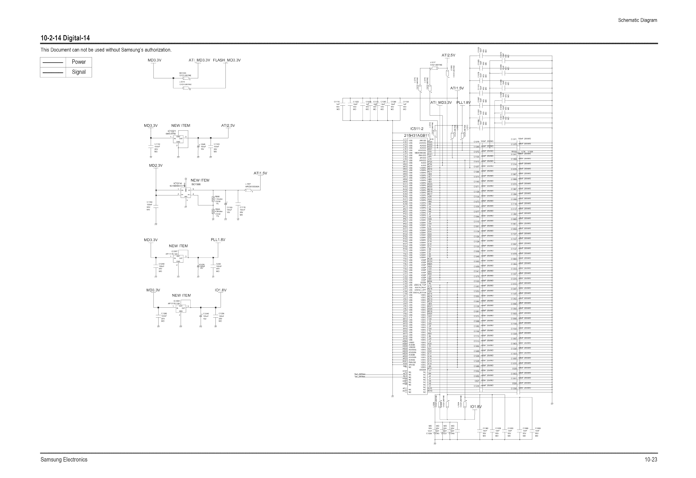
10-2-14 Digitab14
This Document can not be used without Samsung's authorization.
Power MD3.3V
Signal
ATI MD3.3V FLASH MD3.3V
MD3.3V NEW ITEM ATL2.5V
MD2.3V
ATL 1.5V
_tj NEW ITEM .........
]Pff91A ,,
i
g_!2g
MD3.3V PLL1.8V
MD3.3V IO1.8V
IC511-2
215H31AGB11
ATL2.5V
L1217
ClC21J6OINE
Cla711_nF 2_VMO
_VMU
CIO8_
v__v_:_.............
. _ IZ_
Schematic Diagram
SamsungElectronics 10-23

J -n-sdiag-10-a2.qxd 2005-05-23 o_ 12:03 qlolx]10-24
i1
Schematic Diagram
10-2-15 Digital-15
This Document can not be used without Samsunc
D2.5V
T L401MPZ2012S300A
C1346
100uF
Power _
Signal cla21
100nF
25V
MATERIAL
's authorization. DNIE 1.2V
, NEW ITEM
IC413 s_ SC1566
SC156615M-X.X.9_ _
ONO
25V
MATERIAL
+ C1319
100uF
10V
REPLACED ITEM PLL
L1205 IC407 _3
ClC21J601NE RT9183-12 JTOUT
C1303
01293I÷ --L- c156
°°uFI 7°°n T oon
10V 25V 25V
MATERIAL MATERIAL
.2V
+ C1294
Z100uF
10V
SCl CLK
SC2_CLK
SCI_DATA
S C2_DATA
ADV M CLK[_:::>
ADV M B(0:7)
ADV M G(0:7)
ADV M HSYNC D
ADV M R(0:7)
ADV M VSYNCE_:>
R434
0
1/16W
_ reSTMODE
CLK SC01
AF18
CLK SC02
AD21
DATA SC01
AC21
DATA SC02
E23
DEC CLK
ACS FB mN00
FB D_N01
FB D_N02
I FB DIN05
FB D_N06
FB D_N07
FB D_N08
FB D_N09
FB D_NI0
FB D_N13
FB D_N14
FB D_N15
FB D_N16
FB D_N17
FB D_NIS
FB D_N19
FDECODERBLU_N00
FDECODERBLU_N01
FDECODERBLU_N02
FDECODERBLU_N03
FDECODERBLU_N04
FDECODERBLU_N05
FDECODERBLU_N06
FDECODERBLU_N07
FDECODERBLU_N0S
FDECODERGriN _N01
FDECODERGriN _N02
FDECODERGriN _N03
FDECODERGriN _N04
FDECODERGriN _N05
FDECODERGriN _N06
FDECODERGRN_N07
FDECODERHSYNC_N
FDECODERRED _N00
FDECODERRED _N01
FDECODERnED _N02
FDECODERnED _N03
FDECODERnED _N04
FDECODERnED _N05
FDECODERRED _N0S
FDECODERRED _N09
FDECODERVSYNCEN
IC402_2
DNIE4
B _2CSDA
SDP,_MSC02
SDRAMSC01
SCANENABLE
SCANTESTMODE
PLL ON
NRESET
NAND ENABLE
INPUT CLK
}2C SCL
_2C ADD R01
FR D_NIS
FR D_N17
FR D_N16
FR D_N15
FR D_N14
FR raN13
FR raN12
FR raN11
FR raN10
FR raN09
FR mN0S
FR raN07
FR raN06
FR D_N05
FR raN04
FR raN03
FR raN02
FR D_N01
FR raN00
FOSDPOINT
FHSYNC_N
FG mNm
FG mNm
FG raN17
FG mNm
FG raN15
FG raN14
FG raN13
FG raN12
FG D_N11
FG D_NI0
FG raN09
FG mN0S
FG raN07
FG raN06
FG raN05
FG raN04
FG raN03
FG raN02
FG D_N01
FG raN00
DQ(0:63) D 0 D_
D 1 C3
AI
A2
B3
DQ6 A3
C4
D 15 BS
C7
_ B9
C10
D 28 BI0
D 29 AI0
De31 BH
C17
B17
A17
Cm
IC402-4
DNIE4
B FSDP,_MDATA00 O SDP,_MCLK
B FSDP,_MDATA01 O FSDP,_MNWE
B FSDP,_MDATA02 O FSDP,_MNRAS i
B FSDP,_MDATA03 O FSDP,_MNCAS i
B FSDP,_MDATA04 O FSDP,_MDQM i
B FSDP,_MDATA05 O FSDP,_MBANK01
B FSDRAM DATA06 O FSDRAM BANK00
B FSDRAM DATA07 O FSDRAM ADDRI0
B FSD_M DATA08 O FSD_M ADDR09
B FSD_M DATA09 O FSD_M ADDR08
B FSD_M DATA10 O FSD_M ADDR07
B FSD_M DATA11 O FSD_M ADDR06
B FSD_M DATA12 O FSD_M ADDR05
B FSD_M DATA13 O FSD_M ADDR04
B FSD_M DATA14 O FSD_M ADDR03
O FSD_M ADDR02B FSD_M DATA15
B FSD_M DATA16 O FSD_M ADDR01
B FSD_M DATA17 O FSD_M ADDR00
B FSD_M DATA18 B FSD_M DATA63
B FSD_M DATA19 B FSD_M DATA62
B FSD_M DAT_0 B FSD_M DATA61
B FSD_M DAT_I B FSD_M DATA60
B FSD_M DAT_2 B FSD_M DATA59
B FSD_M DAT_3 B FSD_M DATA58
B FSD_M DAT_4 B FSD_M DATA57
B FSD_M DAT_5 B FSD_M DATA56
B FSD_M DAT_6 B FSD_M DATA55
B FSD_M DAT_7 B FSD_M DATA54
B FSD_M DAT_8 B FSD_M DATA53
B FSD_M DAT_9 B FSD_M DATA52
B FSD_M DATA30 B FSD_M DATA51
B FSD_M DATA31 B FSD_M DATAS0
B FSD_M DATA32 B FSD_M DAT_9
B FSD_M DATA33 B FSD_M DAT_8
B FSD_M DATA34 B FSD_M DAT_7
B FSD_M DATA35 B FSD_M DAT_6
B FSD_M DATA36 B FSD_M DAT_5
B FSD_M DATA37 B FSD_M DAT_4
B FSD_M DATA38 B FSD_M DAT_3
B FSD_M DATA39 B FSD_M DAT_2
B FSDRAM DATA40 B FSDRAM DATA41
i
:DNIE 3.3V From DECODER IC Sheet5
C1287 C1286
C408 10nF lnF
47uF 50V 50V
16V_ MO
AD2S R422 ,_AA_._L_._<'--ISDA DD0
-- _ SC2-SDRAM
_ 4_SC1 SDRAM
AD24 R41_ _ '_
AE25 R436
....AF22 R431R426 220ohm _ _DNIE nRESET
AO_ _ HD CLK _ c1624
A_ -- SCL DD0 100nF
AC25 _ _ 25V
HD VSYNC MATERIAL
"------<_ HD DATA(0:11) 7;
AF12 D
AEI2 ]
ADI2 HD DATA(2)/
AC12 HD DATA(3)/
AF13 HD D_T_(4_/
AEI3 HD D_T_(_/
AF14 H# #_Thr71/
ADI4 H# pAT_(£)/
AF15
R860
68ohm
D15
_ DNIE_NWE
DNIE NRAS
DNIE NCAS
DNIE-DQM DN_EBANK_/
DI3 DN_E BANK(0)/
A16 D_rF _PPR_lm/
B16 DN_E ADDR(9_/
C16 DNE ADDR(8_/
A15 DN_E ADDR(7_/
BI_ _N_FADD2__/
c1_ nN_F
A14 DNE ADDR(4)/
B14 DNE ADDR(3)/
C14 DN_E ADDR(2)/
A13 DN_F_DDR(11/
B13 DNE ADDR(0_/
C2S pqr_zl/
B2S P_I_/
A2S nem_/
B2S _em_/
A25 P_#_//
A24 p_q/
C24 DQ(551/
A2S _e¢_m/
B23 Dq(53)i
C23 DQ(52)f, z
A22 DQ(51),i
B22 DQ(50)i
C22 PQ(4_)/
A21 pQ(_7_/
B21 #_r4#//
C21 [30(451/
A20 nQ_d
B20 DQ(43)!
C20 DQ(42) /
A19 P9(41//
HD HSYNC
[]]::> SDRAM CLK
DNIE BANK(0:1)
--[[[_> DNIE ADDR(0:10)
DQ(0:63)
PLL 1.2V
IC402_1
DNIE4
GND
GND VDD48
GND VDD47
GND VDD46
GND VDD45
GND PWR 02
GND PWR 02
GND PWR 02
GND PWR 02
GND PWR 02
GND PWR 02
GND PWR 02
GND PWR 02
GND PWR 02
GND PWR 02
GND PWR 02
GND PWR 02
GND PWR 01
GND PWR 01
GND PWR 01
GND PWR 01
GND PWR 01
GND PWR 01
GND PWR 01
GND PWR 01
GND PWR 01
GND PWR 01
GND PWR 01
GND PWR 01
GND PWR 01
GND GND75
GND GND74
GND GND73
GND GND72
GND GND71
GND GND70
GND GND
GND GND
GND GND
GND GND
GND GND
GND GND
GND GND
GND GND
GND GND
GND GND
SC1 CLK
SC2-CLK
SC1 DATA
SC2-DATA
SC1SDRAM
SC2 SDRAM
i
i
i
i
R1_59
1/16W
DNIE 3.3V
R427
DN]E4 OUTPUTPATH CURRENT CONTROLLER 0
R428 1/16W
r} 1AA,
| _ R4,30 4'A'A% 0
| | 0 A_A_Av 1/16W
___ o
1/16W
R1258 R1256 R1255
1/1Ow 1/O6w 1/1Ow
R1257 R1254
1/106W 1/106W
DELETE
DNle Y(0:7)<_]--
AF21
AD20
AC20
AD19
AF19
AEI9
AE22
AC22
AClS
AC14
AC11
ACS
AC4
A_23
W4
T23
A81
Jl
_7--
F7
F_
E_
DNle PB_0:7_ -..__ \ ......... _ E_
\......... _1_1_RAlOl E_
\_, L _ _" DI
\DN_ PB_ _l_'A'hl - RA100 c2
1/16W
\ 47 BI
DNle DE R1231 .... 47 AAI
P3
P2
N3
.1
\DNle Y(I/ _1_/_/_1 _ RA409 u
_'° 47 K2
\ON,_o, 7J_l: 1,1_w ,,
",DN_ YF) _° 47 J2
YI
DNIE 1.2V
DNIE 3.3V
__]
01275
100nF
c1276
100nF
100nF
C1716
100nF
C124o
100nF
Clp_l
100nF
C#P4
_1949
100nF
C1264
100nF
Q1221
100nF
G_R
100nF
C19R_
C19RR
100nF
GIPR7
100nF
_194R
1##nF
DQ(
0 BANAD_M_NG
O BDATAB OUT00
O BDATAB OUT01
O BDATAB OUT02
O BDATAB OUT03
O BDATAB OUT04
O BDATAB OUT05
O BDATAB OUT06
O BDATAB OUT07
O BDATAB OUT0S
O BDATAB OUT09
O BDATAB OUT10
O BDATAB OUT11
O BDATAB OUT12
O BDATAB OUT13
IC402-3
DNIE4
o PLL P1080 F_LTER
0 PLL MMU F_LTER
O OUT DWCLK
O OUT CLK
O FNRPOST TRSENC DATAOUT R09
O FNRPOST TRSENC DATAOUT R08
O FNRPOST TRSENC DATAOUT R07
O FNRPOST TRSENC DATAOUT R06
O FNRPOST TRSENC DATAOUT R05
O FNRPOST TRSENC DATAOUT R04
O FNRPOST TRSENC DATAOUT R03
O FNRPOST TRSENC DATAOUT R02
C406 1.8nF
_ELETE I [_::>DNle CLK
¥_ ,_-_z'zs"-47_"_ r----------------q--_NR OUT CLK
A_ _ I _._._._._.__F--<>NR-OU T-V
.... R12_.__L_'A' A" 22 J I r----------I_-_NR-OUT-H
AC2_ R1248 22
_26 _ '° 1/16W NR OUT R(5)
_° 47 NR OUT R(4)
R24 _ _ NR OUT R(3)
R23 RA41 1 NR _T R_
P26 _" _ 1/16W NR QUT R(I_
P25 47 NR OUT
P24 _N
o BDATA B OUT14
O BDATA B OUT15
O BDATA B OUT16
O BDATA S OUT17
O BDATA B OUT18
O BDATA B OUT19
O BDATA EN POSTOUT
O BDATA G OUT00
O BDATA G OUT01
O BDATA G OUT02
O BDATA G OUT03
O BDATA G OUT04
O BDATA G OUT05
O BDATA G OUT06
O BDATA G OUT07
O BDATA G OUT08
O BDATA G OUT09
O BDATA G OUT10
O BDATA G OUT11
o FNRPOSTTRSENCDATAOUTR01
O FNRPOSTTRSENCDATAOUTR00
o FNRPOST TRSENC DATAOUT G09
O FNRROST TRSENC DATAOUT G08
O FNRPOST TRSENC DATAOUT G07
O FNRPOST TRSENC DATAOUT G06
O FNRPOST TRSENC DATAOUT G05
O FNRPOST TRSENC DATAOUT G04
O FNRPOST TRSENC DATAOUT G03
O FNRPOST TRSENC DATAOUT G02
O FNRPOST TRSENC DATAOUT G01
O FNRPOST TRSENC DATAOUT G00
O FNRPOST TRSENC DATAOUT B09
O FNRPOST TRSENC DATAOUT B08
O FNRPOST TRSENC DATAOUT B07
O FNRPOST TRSENC DATAOUT B06
O FNRPOST TRSENC DATAOUT B05
O FNRPOST TRSENC DATAOUT B04
O FNRPOST TRSENC DATAOUT B03
O FNRPOST TRSENC DATAOUT B02
N26
_24
W23
V2S
V25
V24
V23
U2S
U25
U24
T2S
AB25
AB26
AA2S
A_25
A_24
Y26
Y25
Y24
0 BDATAG OUT12
O BDATAG OUT13
O BDATAG OUT14
O BDATAG OUT15
O BDATAG OUTm
O BDATAG OUT17
O BDATAG OUTm
O BDATAG OUTm
O BDATAR OUT00
O BDATAR OUT01
O BDATAR OUT02
O BDATAR OUT03
O BDATAR OUT04
O BDATAR OUT05
O BDATAR OUT06
O BDATAR OUT07
O BDATAR OUT0S
O FNRPOSTTRSENCDATAOUTB01
O FNRPOSTTRSENCDATAOUTBOO
BY S'NC POmOUT
O BPWMD_M_NG
_H SYNCPOSTOUT
O BDATA R OUTm
O BDATAR OUTm
O BDATA R OUT17
O BDATA R OUTm
O BDATA R OUT15
O BDATAR OUT14
O BDATA R OUT13
O BDATA R OUT12
O BDATA R OUT11
O BDATA R OUT10
O BDATAR OUT09
NR OUT G(07)
.n _T_z .._--_NR OUT B(0:7)
_ 1/16w NR 9UT _
_° 47 NR OUT B,4,
RA422 NR QLLT
W26 47 NR OUT
w___ _DNle VSYNC
AA3 R1229 ,_/ 22 J _DNle[HSYNC
A_2 I --
AA2 R1230 ._zzzzzzzz_22 iJ .4,--{_>DNle PR(0:7)
R2 _ _ RA420 DNle PR(6)
R3 _ _ _ 'o 1/16W _N_ Pn_/
TI 47
72 _
T3 _ _ RA424 _NI_pRr_
T4 _ _ 1/16W _N!¢
Ol
U2
U3
W
DNIE DQM
DNIE-NWE
DNIE NCAS
DNIE-NRAS
DNIE BANK,
DNIE ADDRI
DNIE DQM
DQ,
DQ(
DNIE DQM
DNIE-NWE
DNIE NCAS
DNIE-NRAS
DNIE BANK,
DNIE ADDRI
DNIE DQM
DQ,
D5V
DNle NR EN
NR OUT B(0:7) N_oo_B(0)
NR OUT B(I)
NR OUT B(2)
NR QUT B(3)
NR OUT B(4)
NR OUT B(5)
IC1228
QS34X245-Q3(REEL)
1_ NC0 VCC3
A0 oE I
AI B0
4A2 BI
A3 B2
A4 B3
A5 B4
A6 B5
A7 B6
NR OUT G(0:7) N_oo__(o)
NR OUT G(I)
NR OUT G(2)
NR QUT G(3)
NR OUT 6(4)
NR OUT R(0:7) Na OUT_(o)
NR OUT R(I)
NR OUT R(2)
NR QUT R(3)
NR OUT R(5)
NR OUT R(6)
XREF
NR OUT V XREF
NR OUT H
NR OUT CLK D XRSF
7PMLL4148 25V
100nF
25V 100nF
100nF
C1617
GND0 B7
NCl VCC2
AS OE 2
A9 BS
AI0 B9
A11 BI0
A12 B11
A13 B12
A14 B13
A15 B14
GNm B15
NC2 VCCl
A16 OE 3
A17 Bm
Am B17
Am Bm
A20 Bm
A21 B20
A22 B21
A23 B22
GND2 B23
NC3 VCC0
A24 OE 4 i4S
A_s B2_ 4_ , RA128_ XmEF_> HDMI VSYNC
46 22 XREF
..... _2 ..... :::_ HDMI HSYNC
..... __ HDMCCLK
_9 B2S i43
A30 B29 4
AS1 BS0
GND3 B31
DNIE 3.3V
1L818
ClC21J601NE
0:7)
IC806
K4S643232E-TC60
VSS
DQ15
VSSQ
DQ14
DQ13 !
VDDQ
DQ12
DCH1 i
VSSQ
DQ10
DQ9
VDDQ
NC
VSS
DQM1
NC
NC
CLK
CKE
A9
A8
A7
A6
A5
A4
A3
DQM3
VSS
NC
DQ31
VDDQ
DQ30
DQ29 1
VSSQ
DQ28
DQ27 1
VDDQ
DQ26
DQ25
VSSQ
DQ24
IC105
DQ14
DQ13
VDDQ
DQ9
CKE
VSSQi
DQ28i
DQ251
VSSQi
DQ24!
VSSi
_DNIE DQM
SDRAM CLK
IDNIE ADDR(0:10)
<::{[[] DNIE DQM
<:{[[] DNIE DQM
SDRAM CLK (o:1o)
<:_ DNIE DQM
SamsungElectronics 10-24
i
/Tx
'\ _
i
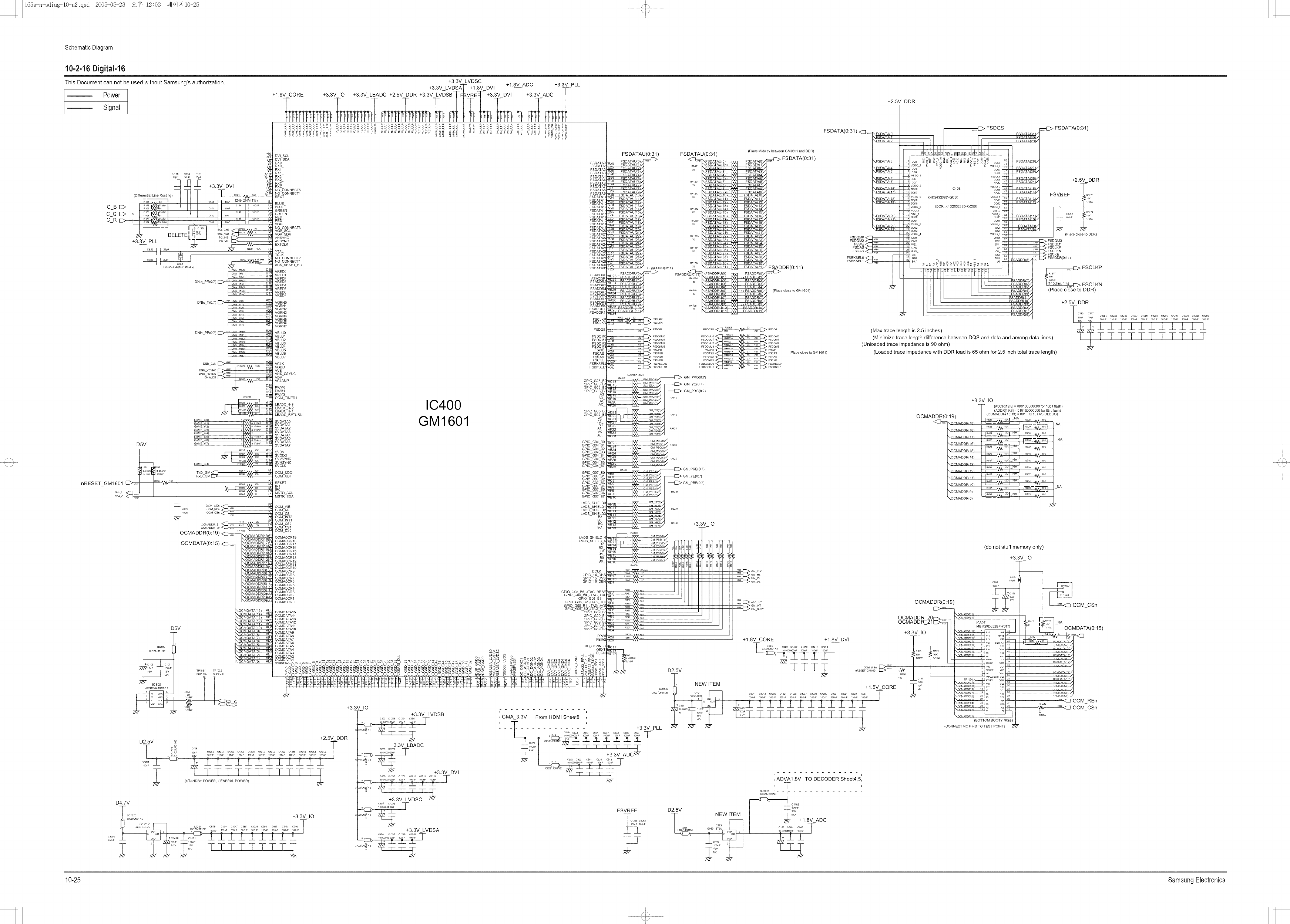
J -n-sdiag-10-a2.qxd 2005-05-23 o_ 12:03 ql o] x]10-25 /L 1
Schematic Diagram
10-2-16 Digital-16
This Document can not be used without Samsung's authorization. +3.3v LVDSC
+3.3V LVDSAT +1.8V DVl +1.8V ADC +3.3V PLL
Power +1.8__B_ DC_V_S_tV_E_._ I +_Aj
+2.5V_DDR
Signal
C136 C134 C133
/0pF /0pF /0pF B1
zlzl-q +33vov, A
(Diffe'entia' Line R°uting7 E _ E
_--2/7-q_ H H II ..... !1 .... (249OHM,1%)B"
C_ B 75°hm C141 10 F C144 _IO_/P B_...... } 111::.......
--F_-------_.--' r4_-_-q _
8nSCL CH2 R870 22
+3.3V PLL LT_ PC2VS_ ^. _'_
HC4_/S SMD04 _lSlSMHZ_
DN_ pR@
DNle mR/I/
DN_ PRm_
DNle PR(0:g) _×_ F DNleDNISDNleDNleDNlePRF)PRm/PR/5/PR/4/PRI3/
A23
X_aFDNle Y(0)
DN_e Y(0:7) DN_ Y(I) U22
DN_ Yr21 _22
l DN_ Yr31 A22
DN_ Y_4/ U21
DN_ Yr51 U21
DN_ YrS/ _21
_ YIT) A21
DNie PB(0:7)
D5V
nRESET_GM16_1 _ 1°°
C_2_
DNle CLK XR_F A20
DNle HSYNC XREF Ul5
DNle DE XReF D2C
C2_
DELET_ U_
IIII
GAME YI0/ 1 2 01_
GAME Y(27
GAME Y_3_
GA_,_EYi4i
GAME Y(5_
GAME Y(6)
GAME Y(7)
R_25 1OK A17
lOK A14
GAME CLK
TxD GM R857 1® M
RxD_ GM
K"
OCM-CSn
L1
R514 22
OCMADDR 21 22
OCMADDR-20
OCMADDR(0:19) _ ....
OCMDATA(0:15)
D5V
BDI00
CIC21J601NE
±._clos c107
10uF 100n_
/6V /6V TP1031 TP1032
_MO SUPLVAL SUPLVAL
A_24C_4_ICSC2ZI_ _1_1/16W __ SCL G
RI SD/_G
D2.5V
D4.7V
BD1026 +3 3V IO
CIC21J601NE ' --
IC1212
AP1117 33 L120_ C949 C12_ C1247 C955 C1233 C950 C947 Cg48 C94_
CC2 J60 NE _F _F O_F O_F _F _F _F _F
C12_0 1 _ lOm,F n n ' ' ' ' ' '
100hE 2 82UF 100nF
6 3V 16V
iiiiiiiiiiiiiii iii iii iiii iiiii .......
_i_ :::_ ::_ _ _ :: :;:;:_;:; _t_ [C>FSDQS FSDATA(0:31)
_ _ ; ;; _ _ _ _ _o_°_ FSDATA(0:31)_ ....
(Place Midway between GM1601 and DDR)
DWSCL FSDATAU(0:31 ) FSDATAU(0:31 )
RX0 _4_ _, VDDQ I > _ > > _ VDDQ 8
RX1
RX1
RX2"
RX2 ,N_ +2.5V DDR
mxc _ VDDQ
NO CONNECT5 IC405
NO-'CONNECT4 _ F
REXT _s _ K4D263238D-QC50 vssQ
BLUE _ DQ19 DO12
BLUE-" _ _'DDQ 3 (DDR, K4D263238D-QC50) VDDQ 6
GREEN R_2_2 ___, vss
GREEN- voo ii,{::RED l@nF
RED _4so
NO CONNECT3
VGA SCL
VGA SDA _ VDDQ (Place close to DDR)
AHS_/N c _12o5
AVSYNC ss
EXTCLK
c_
TCLK _ CKE
NO CONNECT2 ,t_ MCL 'FSADDR(0:117
NO-'CONNECT1 _1214 _ _ _ AS --
ACS RESET HD FSADDRU(0:117 _ _,'/_ FSADDR(0:11 ) '_ _ _ _ '__ _ '_
VRED2VREDlVRED0# !_t'_6_": _ FSCLKP
VRED3 _o_
VRED4{(140°hm_1°/4 EC> FSCLKN
VRED5 _42_ (Place close to GM16017 (Place c_o_seto DDR)
VRED6
VRED7 _s
VGRN0 +2.5V DDR
VGRN6VGRN1 FSCLKh R_)@'"_ 22 _"_' _X_F FSCLKN _428
VGRN2 3s
VGRN3 c_lo c_17
VGRN4 1oF lOP C1285 C12_ C128° C1277 C1289 C1281 C1295 C12_7 C1296 C1282 C1298
VGRN5 FSCLKF . _ ,.. _,_ _F FSCLKP
VGRN7
_:j_ _° _ _soos (Max trace length is 2.5 inches)
FSDQS L26 ×_F _ FSDQSU FSDQSU R12_3 33
VBLU0
VBLu2VBLU1 FSDQM1FSDQM{IZbuzo ilil FSDQMU/....... FSDQMU/, (Minimize trace length difference between DQS and data and among data lines)
VBLU3 FSDQM_UZb FSDQMU2 FSDQMU2" (Unloaded trace impedance is 90 ohm)
VBLU4 FSDQM_ 124 FSDQMU3
VBLU5 FSWE V2_ FSWEU
VBLU6 FSCAS vzo FSCASU (Placecloseto GM16017 (Loaded trace impedance with DDR load is 65 ohm for 2.5 inch total trace length)
VBLU7 FSRAS "1/24 FSRASU
FSCKE W26 FSCKEU
FSBKSEU Y2b FSBKSELU0
FSBKSEL "I'26 FSBKSELU_
VCLK
VODD
VVS
VHS CSYNC (22ohrnX12X4)
VDVLBADC jN3 I. A2AC _ GM PRO(0:7)
VCLAMP GP{O G06 B[ _412 GM PRO0
GPIO-G06-B" GM YO(0:7)
PWM0 GP{O G06-B:
PWM2PWM1 GP_O_ G063B: GM PBO(0:7)
OCM T'MER1 C400 + 3 1 BY-- I O
• (ADDR[19:8] = 000100000000 for 16bit flash)
LBADC }N2
LBADC IN1 GP{O G05 B( (ADDR[19:8] = 010100000000 for 8bit flash)
LBADCIIRETURN GP{O G05 B: _'_'w_'u u r'tur-,r-_ _^r,r, Dm: 1=)m (OCMADDR( 15:137 = 001 FOR JTAG DEBUG)
SVDATA2SVDATA1SVDATA0 GM1601 _ 21 _ .............. _^^_ NAIoK _ NA
SVDATA3 MADDR 1 '" , }
SVDATA4 A00
SVDATA5 '-.(bCMAr_r_R( 17 }
SVCLKSVDATA6 GP'OGP'O_G04IIB7GP'O G04 B0 _G04B2 \OCMADDR(16) 1 ---_yy_I_<_ ..._I°K'NAI _ NA1oK/i ' .... _
SVDATA7 GP{O G04B1 GMGMPBoPBO21 RA423 _ _O'eK1 R522 M_ 1OK
SVDV GP{O G04B3 \('bCMA_R(1_) R520 1OK NA
SVODD GP{O G0484 4 -N' _ RS_SVVSYNC GPIO-G04 B5 GM PBO5 R_25 \OCMADDR(14}
SVHBYNC GP{O-G04 B6 \ ........ (1.} _ 1oK !_ ....
_4_ G ..... GMPRE(0:7) \OCMADDRH2/ _ F 1
OCM UDO GP{O G07 B0
OCM-UD} GP{O G07-B1 _ _GM YE(0:7) \OCMADDRHI_ @_W" 'OKI '_1 ....
GPiO GOT_B2 R404
IR1 GP_O G07B4 : NA
IR0 GP{O G07"-B5
MSTR SCL GP_O-G07"-B6 \()RMAr_r_R(q}
MSTR_SDA GPIO_IG07_B7 OCMADDR(8/ _ NA I ....
LVDS SHIELD0 _
OCM WE LVDS" SHIELD1
OCM-'RE LVDS" SHtELD2 GM YE 2 R_O3
OCM--CS LVDS SHIELD3 GM YE 3
OCM--tNT2 B3
OCM--tNT1 B3 GM YE ,5
OCM]:CS2 BC GM YE6 R'_O_ +3.3V IO
OCM CS1 BC ----
OCM_CS0
OCMADDR19 LVDS SHIELD GM PBE0
OOMADDRI_OOM_DDR1_ LVDB:BN,EL_:_o__ ....
OCMADDR16 BB2 ...... (do not stuff memory only)
OCMADDR15 1 GM PBE 4
OCMADDR14 BB1
OCMADDR13 0 +3.3V IO
OCMADDR12 B0
OCMADDR11
OCMADDR10
OCMADDR9 DCLK
--_, OCMADDR8 GP_O 14 DF
GP{O 15 DVS
OCMADDR6 GP{O][16_DEN
OCMADDR5
OCMADDR4
OCMADDR3 GP}O G08 B5 JTAG RESE
OCMADDR2 GP_O G08 B-4 JTAG TD(
OCMADDR1 GPIO-'G08 B3
OCMADDR0 GPtO G08 B2 JTAG TDt NCIMANNR(N:lq_
GP{O _G08 "_B1 -JTAG "MOI _'"" "_' "\_ "_; OCM CSn
GP{O_ G08_B0 JTAG CL_
OCMDATA15 GP]O Gd§B_
OCMDATA14 GP{O G09 Bz
OCMDATA13 GP{O G09B: OCMADDR
OCMDATA12 GP_O_G0911B:
GP{O G09 B"
OCMDATA11 OCMDATA(0:15)
OCMDATA10 GP_O G09 B(
OCMDATA9 +3.3V IO
OCMDATA8 PPWI--
PBIA_ +1.8V CORE +1.8V DVI
NO CONNEC L815 C253 C 207 C 2 0 C 2 C 2 5
0_ ©Z°OEXT _ cIc21J60_ NE 10 _nF lOOnF lO_F l_g
zzzzzzz
ooooooo
o>o>o>>o>o>o> D2.5V .............
-- RI 7_
C137
lOaF
NEW ITEM +1.8V CORE -r-l_ o
BD1027 _ a
_C40_ _-
GSS3_ST I_,F I_,F I_F I_F loaf lOmF I_,F I_,F I_F I_,F I®F I®F ×_ _] OCM RER
c1_1 1 ' ' n n ' ' ' ' ' ' n n
+3.3V IO ',o_ c.... OCM CSn
-- _ _ 22
_ _:_:" _*_,_+3'3V-LVDSB , GMA__3.3V From HDMI Sheet8 , (BOTTOMSOOT?,90ns) //16w
- -I- ' +3.3V_PLL (CONNECTNCP{NSTOTESTPOtNT)
C14_ C_44 C_2_ C_1 C_27 C_4_ C_S0 C_2S
+2.5V DDR _4 _o_ ................. 0...........
+3.3V LBADC _oon_
_ c252 c_2 c_41 c_ c_42 --
: s LSl_ 100_ F 1_ F 1_ F 1_ F
C_C21J60
+3.gv DVI ' ADVA1.8V TO DECODER Sheet4,5',
BDI0_S ....
C_C21J60_NE
C405 C12S_ _ C1462
........ J FSVREF -- NEW ITEM _o
+3.3V LVDSA _'_ D2.5V _ _o,,_
_ I _ +1.8V ADC
C213 C 5 C C 5
100nF
cl F
10-25 SamsungElectronics
i
/T'_
'\ &/
i
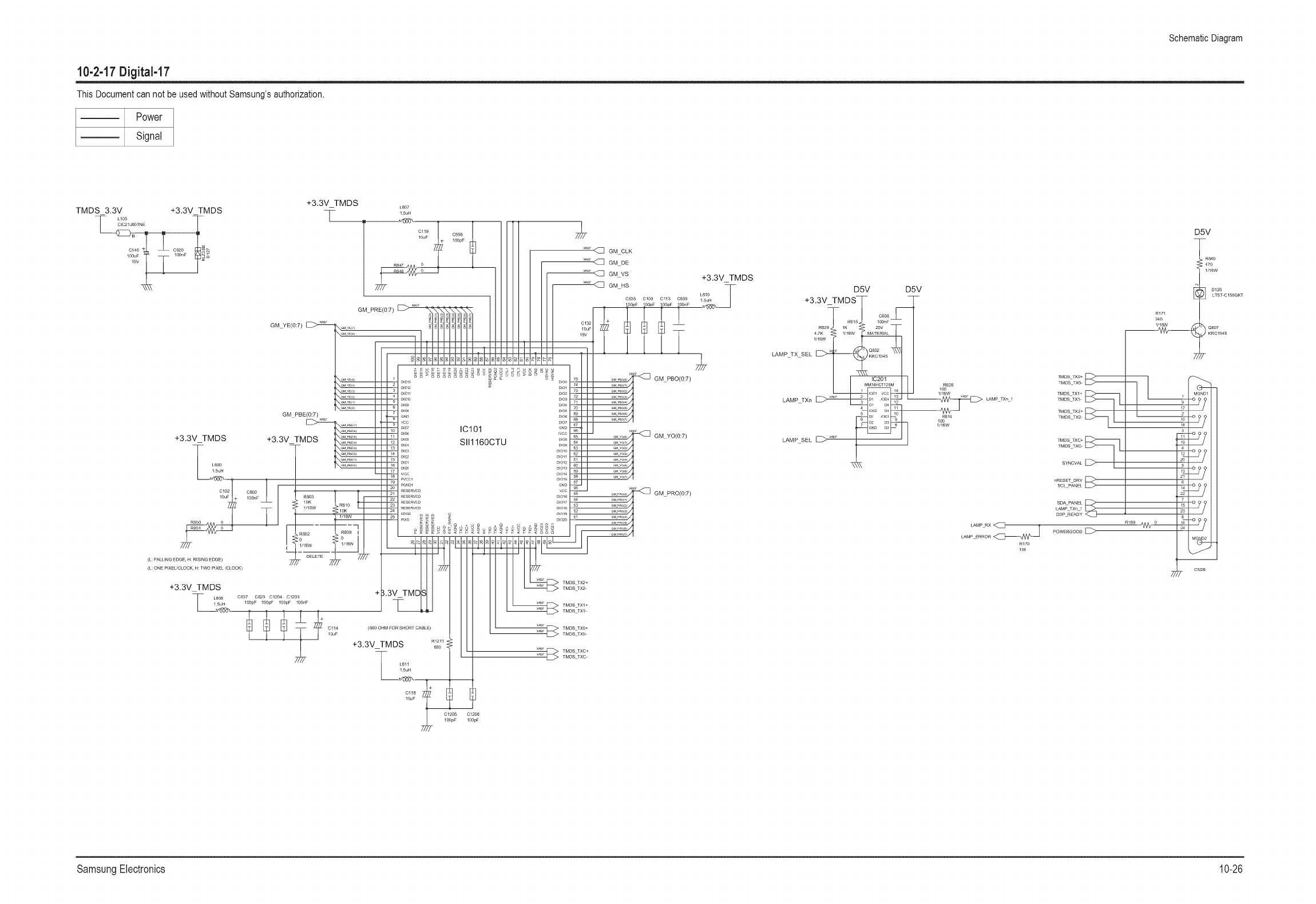
Schematic Diagram
10-2-17 Digital-17
This Document can not be used without Samsung's authorization.
Power
Signal
GMYE(0:7)
+3.3V TMDS
TL807
15uH
Cl19
lOuF
GM PRE(0:7)
+3.3V TMDS
GM PBE(0:7)
+3.3V TMDS
LS00
15uH
(L: FALLING EDGE, H: RISING EDGE)
(L: ONE P]XEL/CLOCK, H: TWO P]XEL/CLOCK)
+3.3V TMDS
L808 C837 C820 C1204 C1203
1 5uH 100pF 100pF 100pF 100nF
Cl14
lOuF
IC101
SlI1160CTU
(680 OHM FORSHORT CABLE)
+3.3V TMDS R_2_
_ 680
L811
1 5uH
TMDS TX2+
TMDS TX2-
TMDS TXI+
TMDS TX1-
TMDS TX0+
TMDS TXO-
+3.3V TMDS
L810
C869 15uH
GM PBO(0:7)
GM YO(0:7)
GM PRO(0:7)
D5V D5V
+3.3V_TMDS T
T. ....Z--
R615 100nF
R629 1K 25V
47K 1/16W MATERIAL
1/16W
LAMP TX SEL
LAMP TXn ×_ 12
LAMP SEL
R171
240
1/16W
___________________
1_ 628
1/16w
--_ LAMp TXn 1
R614
lOO
1/16W
LAMP RX
R170
100
TMDS TX0+
TMDS --_-
TMDS TXI+ --
TMDS TX1- --
TMDS TX2+_>_
TMDSTX2-
SYNCVAL
nRESET DRV
SCLPANEL
SDA PANEL _
LAM_ TXn 1
DDp_EADy
POWERGOOD_
/
9
/7
2
/o
/8
20
_L
22
/5
23
R169 A^A o /e
24
c
MG
• 0
O
O
O
-O
D5V
> R840
470
1/16W
D126LTST-C150GKT
Cl18
10uF
C1205 C1206
100pF 100pF
SamsungElectronics 10-26
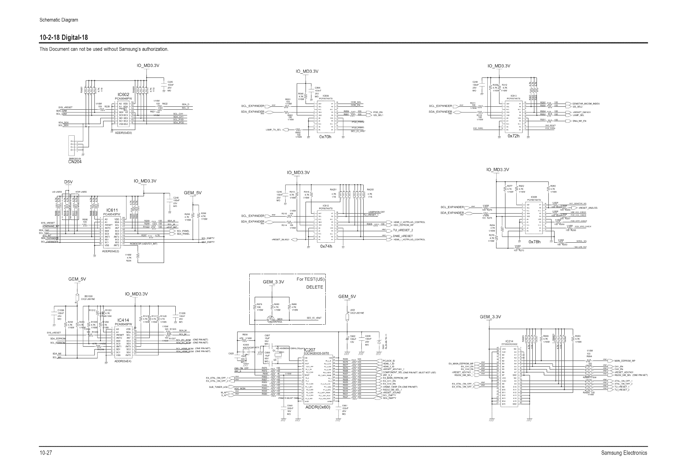
Schematic Diagram
10-2-18 DigitaM8
This Document can not be used without Samsung's authorization.
_._ S IC602
SMW250 04
CN204
IO MD3.3V
I c225
100nF
......... 25V
mew
/00 R622 SDA D
SCL D
SCL Cm
I. I c,.'_ SDA CH1
SCL POD
SDA POD
D5V IO_MD3.3V
usUSED K_ORUSED I
sYs nRESET 100
nO_ENAND_ 4k_--
SCLn_c:NT _
GEM 5V
TR296 < _ R295
47K I 47K
1/16W 1/16W
n_X_INT
ILc:::;;
IO MD3.3V
25v
.... _ = MO pc __C5_7Z_ATS
1/16W I _..........
SCL EXPANDER __ OOB EN
SDAEXPAND_R_/- I _: :: 221., I._ :_.>.....
LAMP TX SEL _ ....
,/¢I,J _ 0x70h
IO MD3.3V
C249 R316
10OnF 47K : 47K 47K : • 47K
MO _ /
1_612
PCF8574ATS
SDA-EXPANDER _V_#
I _ _2 _; !ii ..... DNIE nRESET
0x74h
IO MD3.3V
C248 17_
_nF R3{
25V ......... 4 m
R311
SCL EXPANDER _ _®
SDA EXPAND_ ......... R310
_/16W
POD _,WRS
PCF8574ATS _
_y__--I........ _ R290 .... _ GEMSTAR....... MICOM INDEX
_, R3O4 _OO ....... nRESET GM160_
___ ..... _L
_ 0x72h
_00 R278
R254
47K
U16W
R276 <
47K_ <
m6W
IO MD3.3V
--
GEM 5V
_o_o_ IO_MD3.3V
-
_I R1301
47K
/1 v_/16W R1311
4 7 7K PCA9545PW
SY /RESET SCL 18
/INTO lINT /7
H
ADDR(0xE4)
GEM 3.3V For TEST(US)
DELETE
GEM 5V
R676 R683 R685 =
1/16W 1/16W _ 1/16W L602
C1308 [ CIC21J601 NE
. R1320 l_nF
.... s.........
I N7002L =
mew
1oo R1300 SDA M ....... L ....
•..1_.0OR1307_C_ PC _ (ONE PIN NET) 47 1/16W _5pF tC662
...... RDA PC ROM (ONE PIN NET) IC605 Mo50V _OV 2_
RCI NDMI ROM (ONE PiN NET) KIA7_F _T 12MHz.SOppm{0207
C668
............ (......... ) C620 '0 _ C66; SSC9428X35-SOT8
R677 HDMI I ID
LNA ON OFF 100 ...... HDMI 2 ID
R672 ...... i_ _a, s_ ..... R670 ...... RESETADV7401 1
R666 IK _/16W 7 _:_] K _ _ _1_ 2RP S 2
R663 _ _s pJ z AOII _'_
EX X_AL ON OFF I _E_ - .......... m _ _ i R658
_ .... Ex_aN EEPROUwP
EX_XTAL_O N_O F F_2 R653 io m2 _s R655 EX CH1 EN
R649 ii _2OA_ _IOT0Z O R650 EX CH2 EN
SUB TUNER AGC _AGC MON ..... nHDMI I080p EN (ONE PIN NET)
I 722_z PI 2 I_;a R635 RS232 GM SEL I
M AFT _
S-AFT _E_ nRESET SOUND
R63_ SCL EMPTY
PIN# 15 MUST GNB -!_ ,2_A_ ,2 _ SOA_ SDA EMPTY
.......... 330nF ADDR(0x60) 1O0nF
_MO
GEM 3.3V
EX XTAL ON OFF i m_
EX XTAL ON OFF 2F--"_
1C214
}DTQSS2X245Q2 1 S
1o
13
14
_lS
16
57
.R300
:47K
mew
1/16W
mo
R694
,g__ UA_NEEPROUwP
RA604 100
mew
10-27 SamsungElectronics
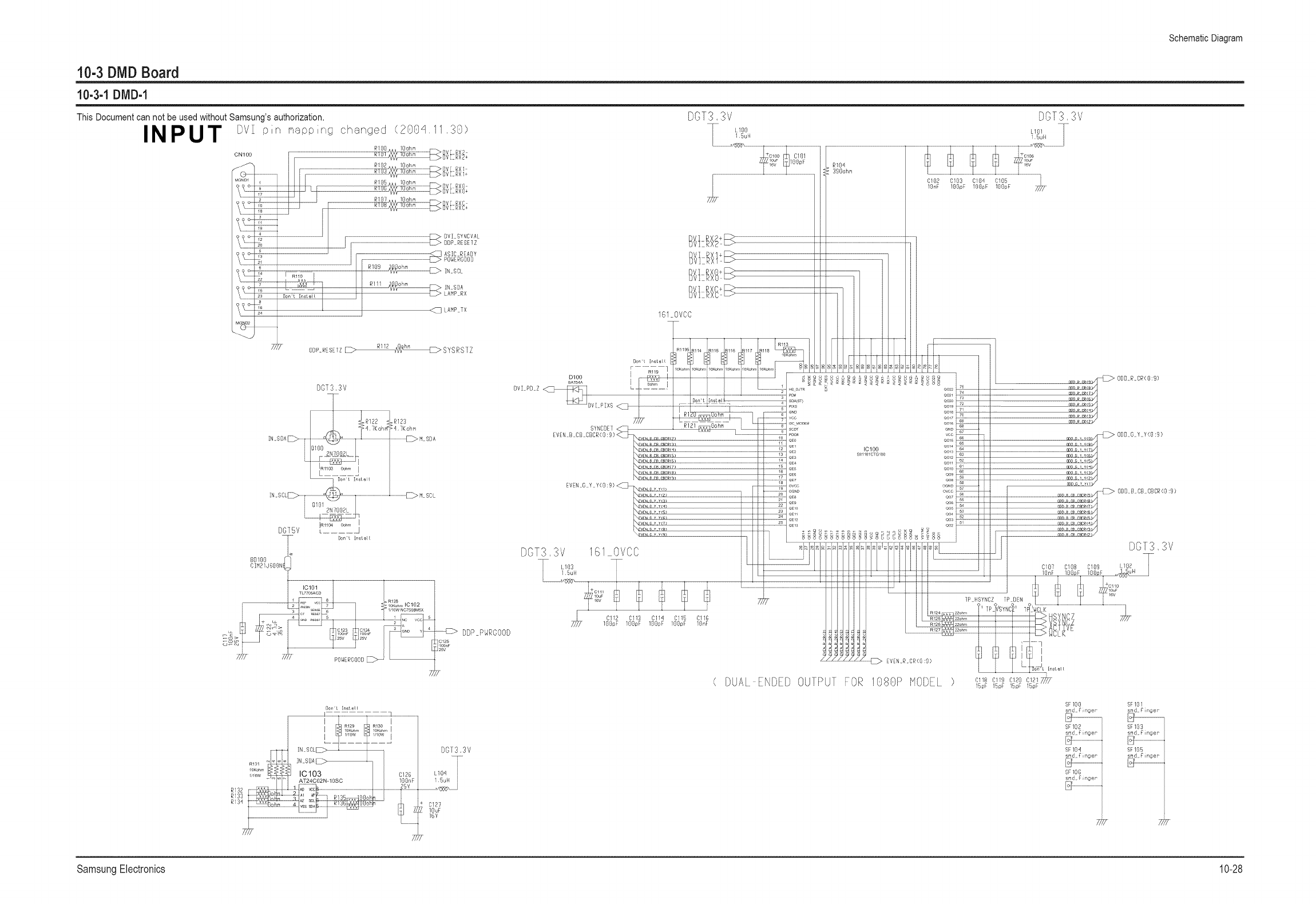
10-3 DMDBoard
10-3-1 DMD-1
This Document can not be used without Samsung's authorization.
IN P U T Dv_o_ _oo_Nooh_oo_d<2Q0_11,;Q>
/777
R132
R133
R13_
_1o9__ IN_scL
IAMP_RX
LAMP 7X
OOP__ESE_Z__SYSRSTZ
DOT3,3V
DDP_P_ROOOD
O_n'_ [nst_lt
J [i ..........................,: L............................................
_N_s0o_---T-_ _ _ors,:tv
IN_SOA
IC103 : 0_26 L104 /
AT24CO2N-lOSC 108n I 5uH |
..................... ............................_v .........................................._, J
4_ /k 0127
I J ' Icl £ lOuF
'1' 16V
7777
DOT3,3V DOT3,3V
( DUAl ENDED OUIPJI FOR 1088P NODEI ) /
0118 0118 0128 0121 77/7
15pF 15pf 15pF 15pF
8FI88
SF1O2
snd_" rig er"
SFlSq
8F186
snd3inger
!.....................................................
,gF181
SF183
snd Fin(let"
l!....................................................
SF185
Schematic Diagram
SamsungElectronics 10-28
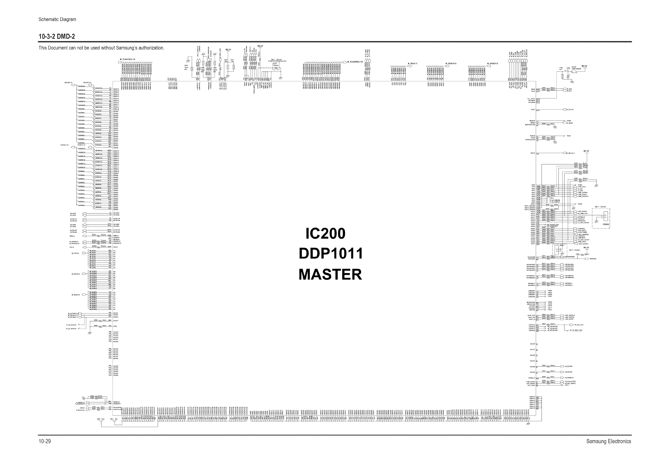
Schematic Diagram
10-3-2 DMD-2
This Document can not be used without Samsung's authorization.
M FLOATA(01_
:,:,_,_,_, _u,_,_,_,_,}_
NN_
_,_,_, ;,_,_,_,_,_,_,_,_,_
_2o
}}??L IC200
DDP1011
MAS'FER
o_
iiiii
10-29 SamsungElectronics
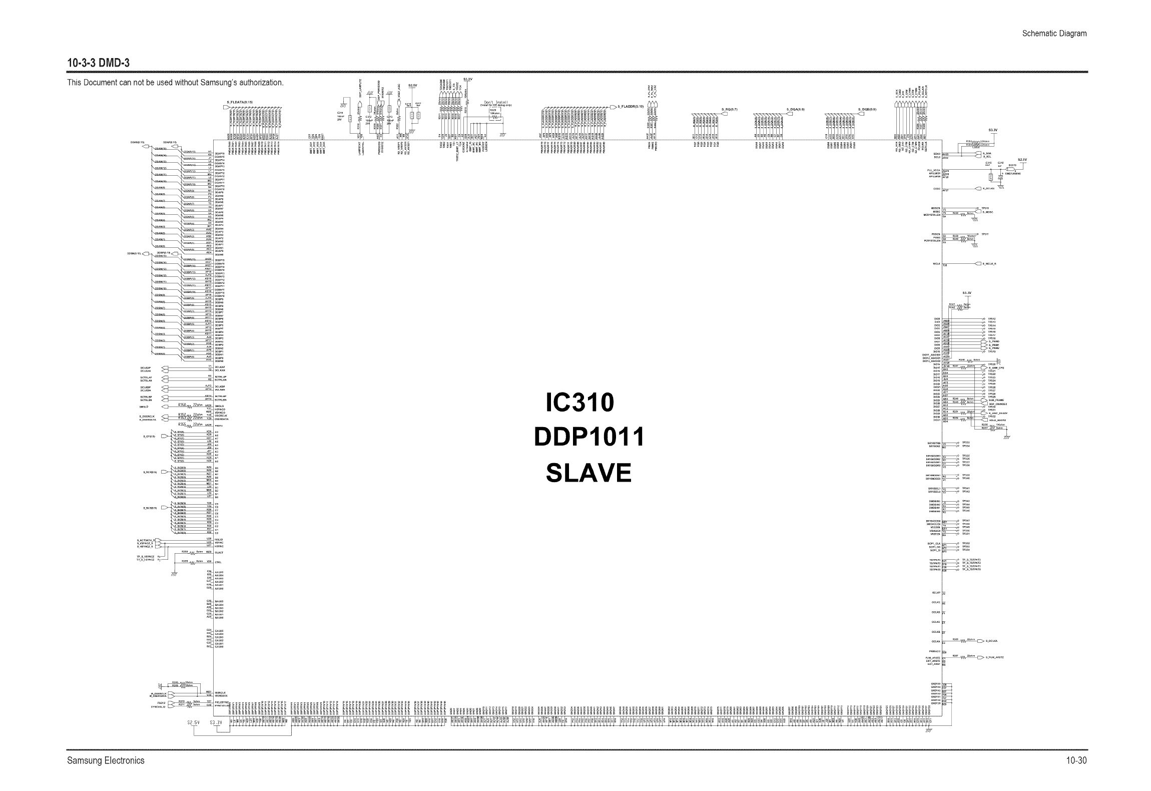
Schematic Diagram
10-3-3 DMD-3
This Document can not be used without Samsung's authorization.
s FLOATA(O1_
_!!!!!!!ii
:,:,_,_,_,
_ sz_v NN_
_,_,_,
sRQ(O:_ s OQA(O:_) s OQB(O:S)
IC310
DDP1011
SLAVE
SamsungElectronics 10-30

Schematic Diagram
10-3-4 DMD-4
This Document can not be used without Samsung's authorization. DGT3.3V
MASTER RDRAM /FLASH
MFLADDR(0:19)
MFL WEZ
M PUM ARSTZ
_M FLADDR!15)
_MM FLADDR(!4!
_MM FLADDR(! _)
_M FLADDR/12 )
_M FI AnnR_11_
_M FI Ar_nR_lm
_U FLADDR_
_U FLADDR_
_M FI ADDR!IB/
_M FI ADDR!17/
_MM FLADDRf71
_MM FLADDRt61
_U FLADDR_)
X'_M FLADDR_
_M FI AnnR_
_U FLADDR_2_
_U FLADDRm
IC400
M29W800DB70N6
1
2 A15 A16
A14 /BYTE
3 A13 VSS
4A12 DQISA 1
5 All DO7
AIO DO14
A9 DO6
A8 DO13
8
9AI9,NC DQ5
10 A20,N C DQI2
11 /WE DQ4
12 /RESET VCC
13 NC DQ11
14
1_/WP,ACC,NC DQ3
1_ RY,/BY DQIO
A18 DO2
17
18 A17 DO9
A7 DQI
19
20 A6 DO8
A5 DQ0
21 A4 /QE
22
23 A3 VSS
A2 ICE
24 AI A0
_M FLADDR[0)
BD40!
} 1.5uH
_ C412
100nF
48
_7
4_
45 M FLDATA[I 5)/
fJ4 M FIr/ATACZ]/
_43 M FIDATA(14//
42 M FLDATA_6) /
41 M FLDATA(!_!//
40 M FLDATA¢5)_
)9 M FLDATAI121/
38 M FI DATA(4//
37
_
36 M FLDATA_! !_
35 M FL DATA_
34 M FLDATA(I O)/
_33 M FI DATA(?)/
°32 M FI DATA!_¢I/
31 M FLDATA_ ! _
30 M FL DATA_
29 M FLDATA[O),
28
o 27
26
2_
MFLDATA(0:15)
MFL OEZ
MFL CSZ
DGT3.3V (CIM21J600NE, 60 OHM, 0.5A, 0805)
(EQUAL LENGTH)
M REFCLK _ 2
M SCLKN _ 7M PCLKM 6
DGT2.5V 15
24
R435 23
1Kohm R436 <<_
1Kohm? 12
11
DGT2.5V __......
1o
7_7
(20MILS, OR WIDER)
CHANNEL IMPEDANCE : 40 OHM)
TRACE THICKNESS : 10Z CU)
LENGTH OF LOADED SEGMENT : 748 MILS)
(20MILS, OR WIDER)
REFCLK
SYNCLKN
PCLKM
MU_O IC402
MU_I CDGR83
so
Sl
s2
PWRDNB
STOPB
VDDFR
VDDFPD
TRACE WIDTH FOR UNLOADED SECTION : 10.4 MILS -> DEPENDENT ON VENDOR)
MINIMUM UNLOADED PITCH : 30 MILS)
FINISHED DIELECTRIC THICKNESS : 8 MILS -> DEPENDENT ON VENDOR))
CLK
CLKB
PAIR, IMPENDANCE: UNLOADED :40 OHM, LOADED:60.6 OHM)
ROUTING: CDCR83-> RDRAM(CTM) -> DDP10t0(CFM) -> RDRAM -> TERMINATION RESISTOR))
(RSL : RQ(0:7), RQA(0:8), RQB(0:8), RD CTM, RDCTMN, RDCFM, RDCFMN, RDCMD, RD SCK)
(50 OHM IMPEDANCE : RDREFCLK, RDSCLKN, RDPCLKN)
(ALL RSL SIGNALS, SCK, CMD, DIFF CLOCK PAIRS MUST HAVE MATCHED ELECTRICAL LENGTH)
R433
[_>20R434
.... _ _7/
R438 MCTMN
110o h m
DGT3.3V
IC403
FAN1117AD-1.8
+ C444
16V /_
T
DGT2.5V
C4Ol c4o3 c4o5 c4o7 c4o9
BD400 C411 C402 C404 C406 C408 C410
coo
C400
100nF 82uF
100nF l_nF 100nF 100nF l_nF 10nF 10nF 10nF 10nF 10nF
MRDRAM1.8V
R400 39.2ohm
39.2ohm
v 39.2ohm
......3_
39.2ohm
M RQ(0:7) G_
M RQ(0) F2
M RQ(I) F6
F7
M RQ(3) _ FT
M RQ(4) Ey
M RQ(5) E6
M RQ(6) E2
M RQ(7)
f (5q0MIL) M SIO
R421
Kohm
M CFM _'_
(POWER ISLAND)
RQQ6 IC401
K4R271669B-SCK8
RQ7
M CFMN
MRDRAM1.8V
AS
M CMD _ SMD
M SCK _ A_ SCK
El
MCTM
M CTMN
CTM
CTMN
CFM
NC2
DQB7
DQBS
DQB5
DQB4 HI
DQB3
DQB2 G2
G6
DQBI
DQB0
Cl
DQA0 C2
DQAI C_
DQA2 BI
DQA3 ........
B_
DQA4 ........
BS
DQA5
39.2ohm
U BOB
U BOB 7
M DQB(6)
M non¢',_
M non¢4_
M DOB 3
M DOB 2
M DQB(I)
D7 A7
CFMN DQA7
AI
NCl ........
D2
M VREF RDRAM fREF
C413 _ R423 A39.2ohm
1OOnF R424 39.2ohm
R427 R428 39.2ohm
39.2ohm R426 ......3_
R428 39.2ohm
R429 39.2ohm
R430 39.2ohm
_/_1"ii_m//_29100F(RDRAM FOR SHORT CHANNEL, 54PIN)R4_I
M DQB(0:8)
(50MILS, OR WIDER)
MRDRAM1.8V
C43! C433 C438 C437 C439 C441 _[_A/_
C430 C432 C434 C436 C438 C440 C442
C445 _
82uF
6.3V
(PLACE NEAR DDP10t0)
R439
C428 427
IOO,,F
10MILS, OR NARROWER)
33ohm
•R441 C443
<" _ IO0,,F
M VREF ASIC
(25MILS, OR WIDER)
M VREF RDRAM
10-31 SamsungElectronics

Schematic Diagram
10-3-5 DMD-5
This Document can not be used without Samsung's authorization.
SLAVE RDRAM /FLASH
S FLADDR(0:19)
S FL WEZ L_S PUM ARSTZ
\s FLADDRrlS_
_s FLADDR(12_
I0500
M29W800DB70N6
1
6
7
8
9
12
13"
14
_£ FI ADDR(18/ 16
_s F_DDR(17_ 17
_S F_DDR_7) 18 IA 7
_S F_DDR(6_ 20_191 A6
_s F_DDR{4) 21 IA4_
_S F_DDR(3_ 22 IA3
_ FLADDR(2/ 23 IIA2
_S FLADDR(I ) 24 AI
DGT3.3V (CIM21J600NE, 60 OHM, 0.5A, 0805)
(20MILS, OR WIDER)
(EQUAL LENGTH)
S REFCLK _ 2
S SCLKN _ 7
S_CLKM 6
DGT2.5V IB
R535 23
Kohm
12
11
DGT2.5V
10
7_7
(20MILS, OR WIDER)
( CHANNEL IMPEDANCE : 40 OHM)
(TRACE THICKNESS : 10Z CU)
(LENGTH OF LOADED SEGMENT : 748 MILS)
oooo
>>>>
REFCLK
SYNCLKN
PCLKM
MU_0 IC502
MU_I CDCR83
so
Sl
s2
PWRDNB
STOPB
VDDIR
VDDfPD
ooooo
zzzzz
(TRACE WIDTH FOR UNLOADED SECTION : 10.4 MILS -> DEPENDENT ON VENDOR)
(MINIMUM UNLOADED PITCH : 80 MILS)
(FINISHED DIELECTRIC THICKNESS : 8 MILS -> DEPENDENT ON VENDOR))
CLK
CLKB
(PAIR, IMPENDANCE: UNLOADED :40 OHM, LOADED:60.6 OHM)
(ROUTING: CDCR83-> RDRAM(CTM) -> DDP1010(CFM) -> RDRAM -> TERMINATION RESISTOR))
(RSL : RQ(0:7), RQA(0:8), RQB(0:8), RD CTM, RD CTMN, RD CFM, RD CFMN, RD CMD, RDSCK)
(50 OHM IMPEDANCE : RD REFCLK, RDSCLKN, RD PCLKN)
(ALL RSL SIGNALS, SCK, CMD, DIFF CLOCK PAIRS MUST HAVE MATCHED ELECTRICAL LENGTH)
DGT3.3V
i BD501
11.5uH
C512
100nF
S FLDATA(0:15)
R533 R534
_V_7_y _ 6 2ohm _ S C'I-M
110ohm _ __
c524
c8_
47pF
R588
110ohm
DGT3.3V
IC503
FAN 1117AD- 1.8
+ 0544 ADJ
18v 77_
77,7
DGT2.5V
SRDRAM1.8V
R500 39.2ohm
39.2ohm
39.2ohm
39.2ohm
39.2ohm
39"2°hii
S RQ(0:7)
s RQ(0)
S RQ(I)
S RQ(3)
S RQ(4)
s RQ(5)
S RQ(6)
S RQ(7)
GI
FS
, E2
_1R52t _ (5-10MIL) S SIO
S CMD
m S SCK
S CTM
S CTMN
S CFM
S CFMN [_>--
S VREF RDRAM
528
100_F
(POWERISLAND)
oooooo
> > > > > >
R_ NC2
RQI DQB7
RO2 DQ_
RQ3 DQB5
R_ DQB4
RQ5 DQB3
IC501
R_ DQ_
K4R271669B-SCK8
RQ_ DQBI
DQB0
S_OI
S_O0
SRDRAM1.8V
R501 39.2ohm
39.2ohlt_
39.2ohlt_
39.2ohltl
39.2ohm
39.2ohm 1
39.2oh!!
Jl
J7
He
H7
HI
G2
G6
G7
(RDRAM FOR SHORT CHANNEL, 54PIN)
S DQB(0:8)
(PLACE NEAR DDP1010)
_/_ R539 110ohl i
C526 C527
100nF 100nF
(50MILS, OR WIDER) fiT//
////
SRDRAM1.8V
C531 C533 C535 C537 C539 C541 10MILS, OR NARROWER)
88oh_
C545 + - C543
82uF 100_F
6.3V
S VREF ASIC
(25MILS, OR WIDER)
S VREF RDRAM
SamsungElectronics 10-32

Schematic Diagram
10-3-6 DMD-6
DMD POWER AND RESET DRIVER_T/_:_" This Document can not be used without Samsung's authorization•
R600
iKohm C600
DAD1000
DAD SCpCLK .................................... 7) SCpCK OUTS° .....................................
DAD SCPDO 42 SCPD_ OUT14 77 8 7 ,,l_s 4
DAD SCPD _ SCPDO OUT13 74 226 5 _Rs _s
DAD SELZ SCPEN2 OUT12 72 4 3 , s
OUT11
SR16MODEISR16STROBE MODEISTROBE OUTIOouT9 54_7........... 2268 "_"===,_RS5 MBRST g
SR16MODE0 MODE0 OUT8 ................ _60] ......
SR16SEL1 SELl
SRI6SEL0 SEL0 RAS02
DGT3.3V IG OUT7 DGT3.3V
................ SR16ADDR3 ................... i-_ A3 OUT6 .......
Beslgn Change Uas 10K SR16ADDR2 1_ A2 OUT5 32 43kBRST4
SRIGADDRI _AI OUT4 29 21 , as-
-SR16ADDR0 _ .................. 45 A0 OuT2OUT3 2}27 8 7 ',BRS_2
DAD NTZ /_RQ TO HOST)
TP601 O7 _5
DGT12V BD600 C687 C688 TP602
33uF 0680 0681 0682 47uF D600
°i_ 5c
_c
a_o8 30
_o3(185V 2S 0710 O711
RESETZ
OEZ RO2
VCC
VOFF RA}L7
VOFF RA}L6
VOF_RA}L5
VOF_RA_L4
VOF_RA_L3
VOF_RA_L2
V12 aWL1 VOFF RAIL1
V12 SWL0 VOF_RA L0
VOFF
V12 3
V12 2
V12 I VSREG
VB_ASRaiL7 VRST RAIL7
VB_ASaa_L_ VRS_RA_L6
VB_ASRaiL5 VRST RAIL5
VB_ASRaiL4 VRST RAIL4
VB_ASRaiL3 VRS_RA_L3
VB_ASRaiL2 VRS_RA_L2
VB_ASRaiL1 VRS_RA_LI
VB_ASaa_h0 VRS_RA_L0
VB_AS VRST
..................._ VB_ASSWL VRST SWL
10 VB_ASLH_
8588588S8
C7141oo,,_
soy
0ohm
VCC2 c662 c663 ...........................1
w 1425 V 825v)
76
13
VRST
R609
_IA) 1/4w
5
CZ0_ CZ07
50V 50V
B_08
C_C21JT01NE
C_A_ _
0734
100,,F
25V
IC605
SNZ4LVCI GI 7
77
DGT5V
[_ c717 _ _ .... _ ....
DGT12V _;_::-- 12_OnF 11_vF 12_0v'F
L
I to.........,o,,1,R0,0R0,0 ' '
0720 0721 +0722 100,,_ _ 10_F 100Koh, e2K _,
MOTOR DRIVER __l _ _ 1
_,, _°,I.... 1
m _ _ J luF 3 3nF 1 5nF .....
TP611 TP612 100nF I 0°hm I I I u /0730
C C21J601NE I0604
_N74LVCI GI 4DBVR
_ _ M OCLKB
R627 C733
aT00
BAT54SW
DGT2.5V
DGT2.5V
L601
B_M41_(_<P600S
DGT3.3V
BDS0e.................
M2.5V
TC630 C601 C603 C605 C607 C_g C611 C613 C615 C617 C61g C621 C623 C62S C627
C600 C602 C604 C606 C608 C610 C612 C614 C616 C618 C620 C622 C624 C_6 C628
$2.5V
I0661 C632 C634 C636 C638 C640 C642 C644 C646 C648 C650 C652 C654 C656 C658
C631 C633 C635 C637 C639 C641 C643 C645 C647 C649 C651 C653 C655 C657 C659
M3.3V
$3.3V
DDP1011 POWER
CNBOl
DGT5V
BDS01
CIM21JT00NI
C71_
_C601 _
AD7801BRU
ACT CTL(7) '_
ACT CTL(°) :_
ACT CTL(5) i7
ACT CTL(4) _
ACTCTL(S) i_
ACT CTL(2) .......7 ...............................
ACT CTL(I) is _/V_
ACT CTL(0) i_ R618
R014
o%_Z> .......
d
: R°I_
•om
ACTUATOR
DGT3:3V
BD60g
C M21J600N
R620
IMo_m
77
TP%8
BD611
--_Z_>DB OUT
C_M21J600NE
DYNAMIC BLACK
SMW2_P
7 CN600
10-33 SamsungElectronics
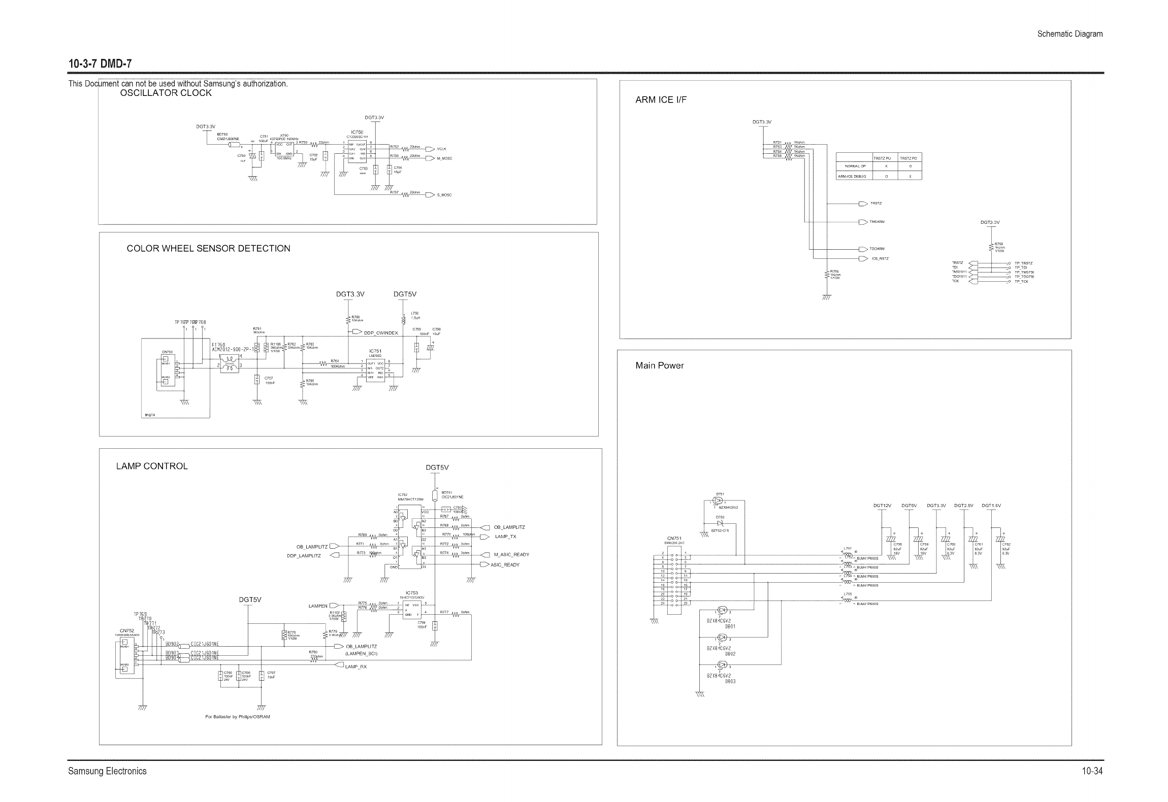
10-3-7 DMD-7
ThisDocJmentcan not beusedwithoutSamsung'sauthorization.
OSCILLATOR CLOCK
DGT3 3V
T ..... 6_1L_: _ R75b _C750
C751 X750 CY2305SC.1H
C[M21J600NE 100 F K375OPCE I_MHz
C750 R755 22ohm M MOSC
C754
15pF
s MOSC
COLOR WHEEL SENSOR DETECTION
TP76"_Tg_768
DGT3.3V DGT5V
C755 C756
DDP CWINDEX 100nF 10uF
LAMP CONTROL
1P769
DGT5V
Fc752
MM74HCT125M
_C753
74HC71G12_GV
DGT5V
BD751
C_C21J601NE
C767
10,,F
LAMP RX
For BalJaster by PhiJips/OSRAM
ARM ICE I/F
Main Power
DGT3 3V
R751 IK_,m --
IKoh,,
IK_,,,
[_>TDOARM
• L_ FCERSTZ
R759
1K_hm
1,10W
DGT33V
TP TMS7_
TP TDOT_
TP TCK
DGT12V DGT5V DGT3 3V DGT2 5V DGT1 5V
= c758 c759 c76o c762
< L751 _ 82vF 82UvF _
s
BZXS4CgV2
_803
Schematic Diagram
SamsungElectronics 10-34
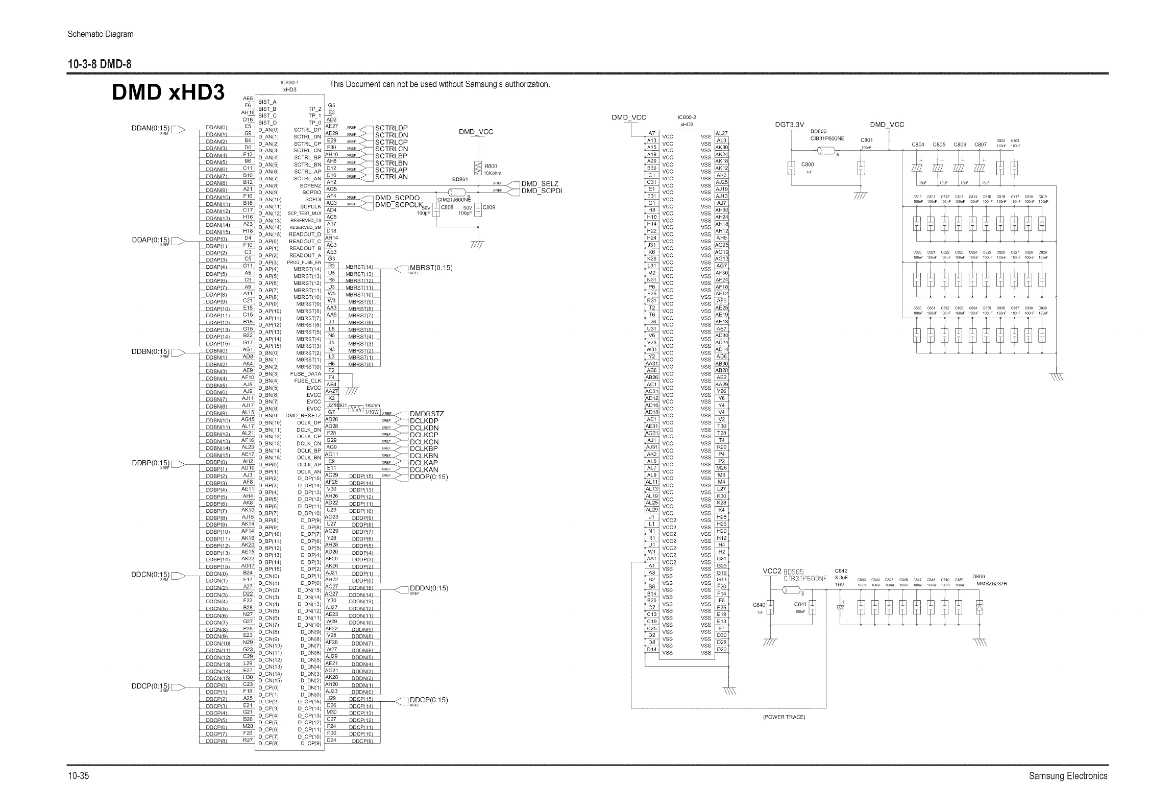
Schematic Diagram
10-3-8 DMD-8
DMD xHD3
DDAN(0:15)
XREF
DDAP(0:!5 t
DDBN(0:!5 t
DDBP(O:_5 t
DDCN(0:!5 t
DDCP(0:!5 t
AE5i
F_
AH_
D_
DDAN(0) E5
DDAN(1 / G9
........DDAN(2/ B4
DDAN(3/ D6
DDAN(4/ F12
DDAN(5) B6
........DDAN(6/ Cl!
........DDANi7i B10 ....
........DDANi8i
DDAN(9/ A21
DDANil0) F16
DDAN(11) B16
........DDAN(12/ C17
DDANi13i H16
........DDANi14i A23
DDAN(15/ H18
DDAPi0) D4
DDAPtli FIO
........DDAPi2i C3
........DDAPi3)
DDAP(4/ Gli
DDAPi5) A5
DDAP(6/ C9
DDAPi7i A9
DDAPi8i All
DDAP(9/ C21
DDAPil0) E15
DDAP(11) C15
DDAP(12/ B18
DDAP(13/ G15
DDAP(14) B22
DDAP(15/ G17
DDBN(0) AG!
DDBN(1 / AD8
DDBN(2/ AK4
DDBN(3) AE9
........DDBN(4/ AF10
DDBNiSi A J5
Z DO_.i6i
DDBN 7 AJI I
DDBN_81 AJ17
........DDBNi9i ALl5
DDBNil0/ AG15
Z DOB.i.i AL£
DDBN(12/ AL21
DDBNi13iAFt6
DDBNi14) AL23
DDBN(151 AE17
DDBPI01 AH2
DDBPili ADI0
DDBP_21 A J3
DDBPi3i AF8
DDBPi4i AEI I
DDBPi5i AH4
DDBPi6i AK8
DDBP_71 AKI0
DDBPi8i AJ15
........DDBPi9i AK:I4
DDBP(10/ AF14
DDBPilli AK16
DDBPi12i AK20
........DDBPi13i AE15
........DDBPi141AK2_
DDBP(15/ AG17
DDCNiO/ B24
DDCNili E17
DDCN(2/ A27
........DDCNi3i D22
........DDCNi4i
DDCN(5/ B28
DDCNi6i N27
........DDCNi7i G2_
DDCNiSi P28
DDCN(10) N29
DDCN(111 G23
DDCN(12) C29
DDCN(13/ L29
DDCN(14/ E27
DDCN(15/ H30
DDCP(0/ C23
DDCPili F18
I DDCP(21 A25
I DDCPi3i E21
DOCPi_iG_
I DDCP(5) B26
I DDCP(6/ M28
I _p_Lz_.......................
L DDCP(81 R27
IC800q
xHD3
BIST A
BIST_B TP2
BISTC TP1
BISTD TP 0
DAN(0) SCTRL DP
D AN(Z) SCTRL DN
D AN(2) SCTRLCP
D AN(3) SCTRL CN
U AN(4) SCTRLBP
U AN(5) SCTRL BN
U AN(6) SCTRLAP
U AN(7) SCTRL AN
U AN(8) SCPENZ
D AN(9) SCPDO
D AN(10) SCPDI
DAN( 11 ) SCPCLK
D AN(12) SCP TEST MUX
D AN(13) RESERVED TS
D AN(14) RESERVED SM
D AN(15) READOUT D
D AP(0) READOUT-C
D AP(1 ) READOUT-B
D AP(2) READOUT-A
D AP(3) PROG FUSE EN
D AP(4) MBRST(14)
D AP(5) MBRST(13)
D AP(6) MBRST(12)
D AP(7) MBRST(11 )
D AP(8) MBRST(10)
U AP(9) MBRST(9)
U AP(10) MBRST(8)
DAP(11 ) MBRST(7)
U AP(12) MBRST(6)
U AP(13) MBRST(5)
D AP(14) MBRST(4)
D AP(15) MBRST(3)
U BN(0) MBRST(2)
U BN(1) MBRST(1)
D BN(2) MBRST(0)
D BN(3) FUSEDATA
D BN(4) FUSE_CLK
D BN(5) EVCC
D BN(6) EVCC
D BN(7) EVCC
D BN(8) EVCC
D BN(9) DMD RESETZ
D BN(10) DCLK DP
D BN(11) DCLK-DN
D BN(12) DCLK-CP
D BN(13) DCLK-CN
D BN(14) DCLK-BP
D BN(15) DCLK-BN
D BP(0) DCLK-AP
D BP(1 ) DCLK-AN
D BP(2) D DP_15)
D BP(3) D DP(14)
D BP(4) D DP(13)
D BP(5) D DP(12)
D BP(6) DDP(11 )
D BP(7) D DP(10)
D BP(8) D DP(9)
D BP(9) D DP(8)
D BP(10) D DP(7)
DBP(11 ) D DP(6)
D BP(12) D DP(5)
D BP(13) D DP(4)
D BP(14) D DP(3)
D BP(15) D DP(2)
D CN(0) D DP(1 )
D CN(1 ) D DP(0)
D CN(2) D DN(15)
D CN(3) D DN(14)
D CN(4) D DN(13)
U CN(5) U DN(12)
D CN(6) D DN(11)
D CN(7) D DN(10)
D CN(8) D DN(9)
D CN(9) D DN(8)
D CN(10) D DN(7)
D CN(11) D DN(6)
D CN(12) D DN(5)
D CN(13) D DN(4)
D CN(14) D DN(3)
D CN(15) D DN(2)
D CP(0) D DN(I )
D CP(1) D DN(0)
D CP(2) DCP(15)
D CP(3) D CP(14)
D CP(4) DCP(13)
D CP(5) DCP(12)
D CP(6) DCP(11 )
D CP(7) D CP(I 0)
D_CP(8) D_CP(9)
This Document can not be used without Samsung's authorization.
G5
E3
AD2
SCTRLDP DMD VCC
SCTRLDN -_--
E_ SCTRLCP
SCTRLCN
SCTRLBP I
SCTRLBN F_q ....
9_ SCTRLAP I_-]_0Kohm
D_ SCTRLAN BD801
AF2 _ [ XREF _ DMD SELZ
AG5 __ DMD-SCPDI
__ DMD_SCPDO IClM2_N_E I _ --
DMD-SCPCLKsov _-_-5o_/[_] C809
,_C5 100pF 100pF
_ga
_Eaa
MBRST(14/ _ MBRST(0:15)
u.' MBRSTi13iI .....
R-_ MBRSTi12i [
U: MBRSTilli I
w_ MBRSTil0i
A_A MBRST(9
MBRSTiSiI
AjI MBRSTi7)
MBRST(6
L_ MBRSTiSi I
N-_ MBRSTi4)
J_ MBRST(3
N{ MBRSTi2i I
L_ MBRSTili
H_ MBRSTi0i I
F£
Xg
d2 _01 IKohm
.G: _ '-_ .... _ DMDRSTZ
AD 26 XREF _ DCLKDP
AD28 XREF _ DCLKDN
F28 XREF <>_ DCLKCP
E9 XREF <>_ DCLKAP
E_ _ DCLKAN
AC29 DDDP(15) _ _DDDP(0:15)
AF26 DDDP(14/ "_ I
V30 DDDP(13/
AH26 DDDP(12)
AD22 DDDP(11 )
U29 DDDP(10/
_,G23 DDDP(9)
U27 DDDP(8)
_,G29 DDDP(7)
Y28 DDDP(6/
AH28 DDDP(5/
A!L20 DDDP(4/ ........
AF20 DDDP(3)
26 DDDP(2)
A J21 DDDP(1 )
AH22 DDDP(0)
_C 27 DDDN05) _ DDDN(0:15)
_,G27 DDDN(14) _XREF
....Y30 DDDN(13)
A J27 DDDN(12)
AE23 DDDN(11 )
W29 DDDN(10/ ........
AF22 DDDN(9) ........
V28 DDDN(8)
AF28 DDDN(7)
W27 DDDN(6/
A J20 DDDN(5)
AE21 DDDN(4/
_AG21 DDDN(3_
AK28 DDDN(2/
AH20 DDDN(I )
A J23 DDDN(0)
J29 DDCP(15/ _ IDDCP(0:15)
D26 DDCP(14/ I _ 'XREF
M30 DDCP(13) _
C27 DDCPf12//
F24 DDCPiI"nI
D24 DDCP(9/ |
DMD VCC IC800_2
xHD3
VCC VSS
VCC VSS
VCC VSS
VCC VSS
VCC VSS
VCC VSS
VCC VSS
VCC VSS
VCC VSS
VCC VSS
VCC VSS
VCC VSS
VCC VSS
VCC VSS
VCC VSS
VCC VSS
VCC VSS
VCC VSS
VCC VSS
VCC VSS
VCC VSS
VCC VSS
VCC VSS
VCC VSS
VCC VSS
VCC VSS
VCC VSS
VCC VSS
VCC VSS
VCC VSS
VCC VSS
VCC VSS
VCC VSS
VCC VSS
VCC VSS
VCC VSS
VCC VSS
VCC VSS
VCC VSS
VCC VSS
VCC VSS
VCC VSS
VCC VSS
VCC VSS
VCC VSS
VCC VSS
VCC VSS
VCC VSS
VCC VSS
VCC VSS
VCC VSS
VCC VSS
VCC VSS
VCC VSS
VCC VSS
VCC2 VSS
VCC2 VSS
VCC2 VSS
VCC2 VSS
VCC2 VSS
VCC2 VSS
VCC2 VSS
VSS VSS
VSS VSS
VSS VSS
VSS VSS
VSS VSS
VSS VSS
VSS VSS
VSS VSS
VSS VSS
VSS VSS
VSS VSS
VSS VSS
VSS VSS
DGT3.3V DMD VCC
BD800 i
ClB31P600NE C801
..........................\ B 100nF
C800
VCC2 BD985 C842
(POWERTRACE)
C802 C80S
C804 C805 C806 C807 100nF 100nF
C810 C811 C812 C813 C814 C815 C816 C817 C818 C819
100,,F 100,,F 100,,F 100,,F 100,,F 100,,F 100,,F 100,,F 100,,F 100,,F
C820 C821 C822 C8Z3 C824 C8Z5 C826 C827 C828 C829
100r,F 100r,F 100r,F 100r,F 100r,F 100r,F 100r,F 100r,F 100r,F 100r,F
C830 C831 C832 C833 C834 C835 C836 C837 C838 C839
100,,F 100,,F 100,,F 100,,F 100,,F 100,,F 100,,F 100,,F 100,,F 100,,F
D800
10-35 SamsungElectronics
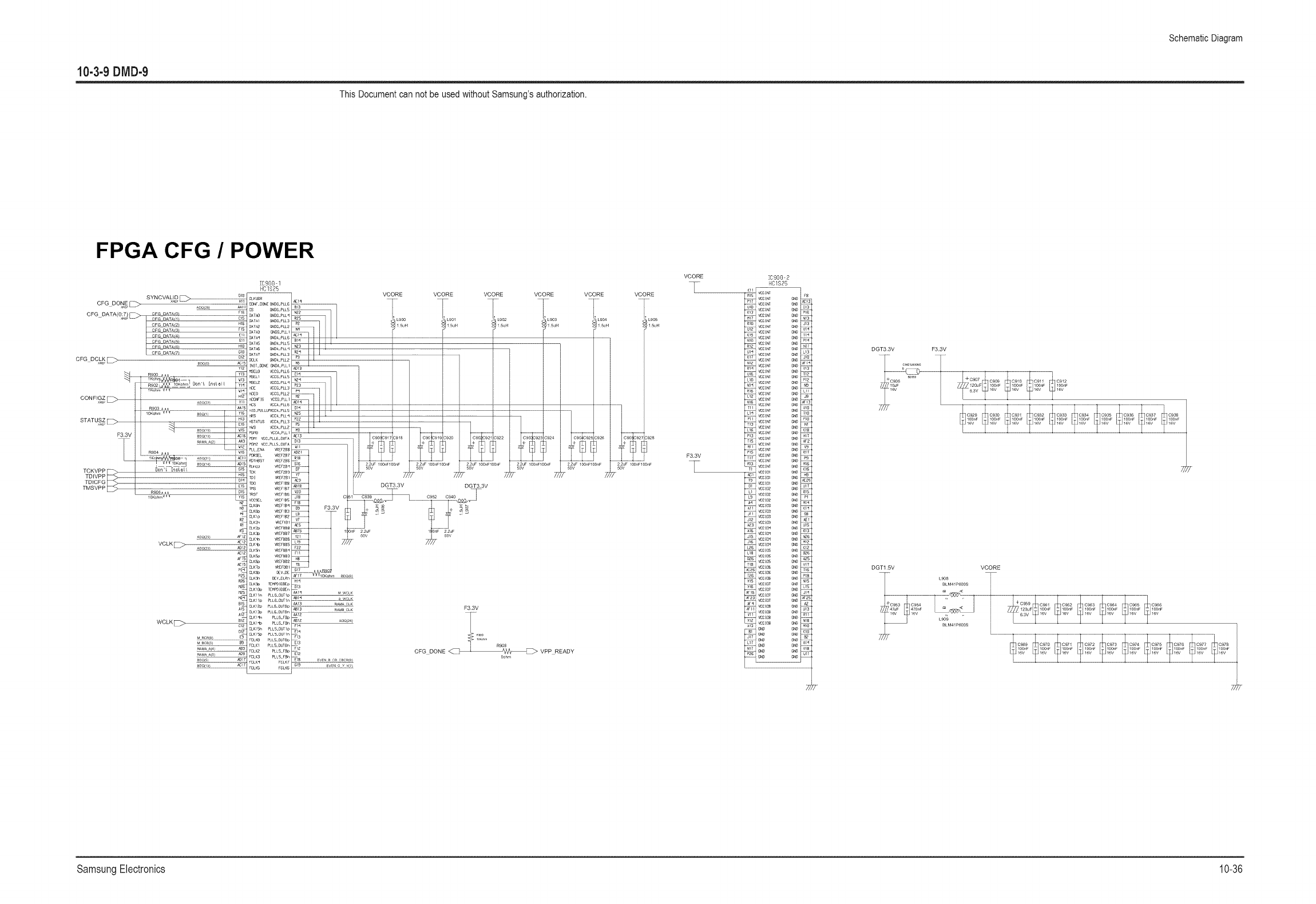
Schematic Diagram
10-3-9 DMD-9
This Document can not be used without Samsung's authorization.
FPGA CFG /POWER
SYNCVALID _ Om
CFG DONE x_F_ _H
n_
CFG DATA(0:7)[ _ _ _EG_ATA(_ ..................................................................................................................
- _-- I CF_ DATAI!! 015
FG DATA_2_ Hf$
EG_0A_AI4L Eli ...._CF9DATA(C) GII
[CFG DATAtB
CFG DCLK [-_ c,
Rgoo
00 t [nstoH _i4"
...... n'
CONFIGZ HI_
R903 ......................................................................_i5
STATUSZ _V BDQ{ yis
BDO(S) W_5
F3.3V BDQ( 3} _C_
C _,MA A(2) _B
R904 !_t5
TCKVPP r_. Don'_ [nst eH GI5
TDIVPP _ HIs
TDICFG ot_
TMSVPP R906 _IS
_rT
ADQ(25) ,_z
VCLKF _ _E_Z
ADOmm _
_C_Z
P_S
WCLK _ Cl_
0m
M RCR_B}
_i T_i_[ .................................
_MA At5)
BDOrS) _7
BDqm mr
IC900 1
HC1S25
a3_r om__U__eu__
G'fD[3PLL5
OAT,_) _NDG_PLL'{
3ATAI 8NDG_PLL3
0ATA_ _DG_PLLZ
0ATA_ G/DB_PLLt
0ATA'_ CNDA=PLL5
DATA5 t_IDAP_L5
OAT_ mDA pLL_
0A_7 C_DApU_
C(;K elo_mLZ
_N_TruNE mP_PH _
_S[Le V;C__PLLS
_LI 'mC_-PLL5
_S_L_ VCO_-PLL_
,_ VOCS_PLLS
_s vccA pLL_
_TUS 'mC_PLL_
_ws VCC__mLZ
_,1 VCO/_LL__0UTA
_'_ V;C_PCLS_OUTA
P_LE_ WEFZ_S
P0_S_ V_EFZ_7
_Yr_SY _E_Z_S
m_LU _EFZ_
TCK _EFZB3
TO[ V_EF2Bt
TOO _EFI_
T_S _EFIB7
_RST WEFIBg
VCC_ V_EFIB5
C_K_ v_EriB_
C_K_ V_EFIB3
%_1p _REFIB2
oK_ V_EFe_S
&K3_ _EFBST
&_; WEFn_5
&_n V_EFeS_
CLK_O _EFe_
O__6o V_EFB_Z
&KYD V_EFOBi
C_K_ _v_o
CLK_ _V_OL_
&K_ T_n_ lors-p
_11n P_S.OUT_
_LKIIo &LB DUTn
,TLK 12p _LLB OUTOp
Domino mLB_OUT8_
oJ<l_ PLL__F_
CLKI#3 F_L&F_
CLK15_ I%LS_DUTIo
___15o _LS_OUT_n
FCLA3 mt 5 ot Te_
_c_KI _LL_O_en
£CLK2 P£L5 F_
_cc<3 PtLSF_
rCCK_ rC_7
FCLK5 fCLKS
VCORE VCORE VCORE VCORE VCORE VCORE
T--TTT
_25 "Lg0o , 901 < 902 " L903 5uH _ 5uH
C90 C98 99:920 92 ;922 C924
_1_ DGT313V DGT3.3V
n_ _ t l @D_, ...........................................l
r_3 FS.3V "_ _ _
Z:_i............ ?= t_=
.....................................i OnF 22_F I OnF 22_F
I
_i_ M WCLK
S WCLK
_13 _& CLK
_13 RAMB CLK
_lZ
_IZ A_C24 }
-€]3
nZ
_Z
_8 EVEN B CB CBCR_8}
_1_ EVEN G Y Y_7}
F3.3V
CFG_DONE _ _ R908
_/_,_ VPP READY
Oohm
VCORE
K11
ms
m7
u_e
TiT
P,io
ulz
_7i7
mz
ur_
KI7
mz
m+l
LIO
_m
L12
ms
fit
L]4
PII
PI3
TI5
P17
F3.3V -77f
TT
_iT
#g
iN
Tg
_N
Tg
IC900 2
H01825
vccl_ _D
VOOIN_ _O
vccl_T _D
VCOINT C_D
VCCl_l mb
VOOINI GNO
rotifer mD
VOClNT mO
_cci_ mD
vccl_ mo
_cl_l ¸ c_o
VCCl_ mb
u;cl_ mD
_CClN_¸ m_
VCClOl mo
_clol a_o
_ccia_
vccia_
_ccla?
vcc_o_
vcc_
vcclo_
vcclc_
vcclr_
_ccl_
_cci_
vcclr_
vcc_c_
vccl_
vcc_s
_ccio7
vcc_o_
_clo7
_ccio7
vcclc_
vcclc_
mo
mo
mo
mo
mo
DGT3.3V
DGT1.5V
F3.3V
L908
BLM41 PBO0S
l:2;d
L_;
BLM4 P600S
VCORE
-[,09.2.... A.... 2.... J_.... 2.... 2....m 120uF763v 16V...... 7 16V...... 7 16V...... 7 16V...... 7 16V...... 7 16V......
......................................_ 7g_} _ ?g;/r7 _72g,_ _ ?g_/r_ _7g£$ _ 7g;/r$ _7@j/rg _ 7g_/r7F1'......................................................................................................................................................................................16V 16V 16V 16V 16V ? ..........................................................................16V I@V ? .....................................16V _ 16V_gC/r}
#,y
SamsungElectronics 10-36
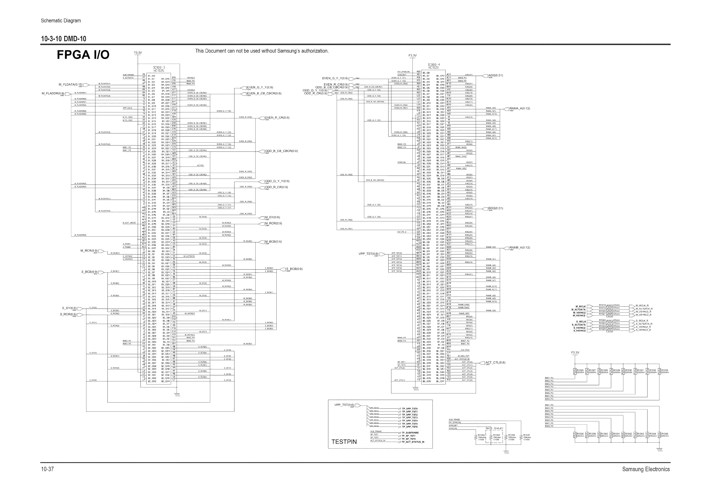
Schematic Diagram
10-3-10 DMD-10
FPGA I/O F3.3V
IC980 3
_,81S25
This Document can not be used without Samsung's authorization.
EVEN_G_Y_Y(O :9) _ _f
ODDe y Y(9}
ODDG Y Y_S>
ODDRCR(S>
ODDRCR(7>
VPP_TST(0:6
F3.3V
18988 '_
H81S25
TESTPIN
_o TP VPP TSTO
o TPVPPTST1
o TP VPP TST2
o TP VPP TST3
O TP VPP TST4
O Tp VppTST5
O TP VPP TST6
SUB FRAME OTP SUBFRA_E
SPTST O TP SP TST1
TP SP TSTO
.................................................0TP ACT STATUS IN
SUBFRAME
DVlSYNCVAL
SYNCDET
SYNCVAL
: 10Kohr_
SOW
F3.3V
BNKIPU
BNK2PU
BNKSPU
BNKaPu
BNK5PU
BNKSpU
BNKrPU
mK_ PU
mK1PD
10-37 SamsungElectronics

10-3-11 DMD-11
This Document can not be used without Samsung's authorization.
SDRAM
DGT3.3V
Ll100
1.5uH
[I_<_
/
C1100 C1101 C1102 C1103 C1104 C1105 C1106 C1107 C1108 C1109 C1110 C11111 J
10uF 100nF 100nF 100nF 100nF 100nF 10nF 10nF 10nF 10nF 10nF 10nF
ADQ(0:31 )
RAMA WEZ
RAMA CASZ
RAMA RASZ
RAMA-CSZ L._r R1100
1Kohm
_ 1/10W
_y
_N_0m/
_ADQ_I_
RAMA_A(0:I 2)
1
2
3
4
5
6
ICl 100
K4S643232E-TC60
VDD VSS
DQ0 DQ15
VDDQ VSSQ
DQ1 DQ14
DQ2 DQ13
VSSQ VDDQ
DQ3 DQ12
DQ4 DQ11
VDDQ VSSQ
DQ5 DQ10
DO6 DQ9
VSSQ VDDQ
DQ7 DQ8
NC NC
VDD VSS
DQM0 DQMI
/WE NC
/CAS NC
/RAS CLK
/CS CKE
NC A9
BA0 A8
BA1 A7
A10,AP A6
A0 A5
A1 A4
A2 A3
DQM2 DQM3
VDD VSS
NC NC
DQ16 DQ31
VSSQ VDDQ
DQ17 DQ30
DQ18 DQ29
VDDQ VSSQ
DQ19 DQ28
DQ20 DQ27
VSSQ VDDQ
DQ21 DQ26
DQ22 DQ25
VDDQ VSSQ
DQ23 DQ24
VDD VSS
ADQ/14)/
RAMA CLK
ADQ/31//
ADQ/28)/
DGT3.3V
Ll101
1.5uH
/
Cl112 Cl113 Cl114 Cl115 Cl116 Cl117 Cl118 Cl119 Cl120 Cl121 Cl122 Cl123} J
10uF 100nF 100nF 100nF 100nF 100nF 10nF 10nF 10nF 10nF 10nF 10nF
BDQ(0:31 )
RAMB WEZ
RAMBCASZ
RAMBRASZ
RAMB-OSZ
\BP0m_
_BDQ_I_
RAM B_A(0:12)
1
2
3
5
IC1101
K4S643232E-TC60
VDD VSS
DQ0 DQ15
VDDQ VSSQ
DQ1 DQ14
DQ2 DQ13
VSSQ VDDQ
DQ3 DQ12
DQ4 DQ11
VDDQ VSSQ
DQ5 DQ10
DQ6 DQ9
VSSQ VDDQ
DQ7 DQ8
NC NC
VDD VSS
DQM0 DQMI
/WE NC
/CAS NC
/RAS CLK
/CS CKE
NC A9
BA0 A8
BA1 A7
A10,AP A6
A0 A5
A1 A4
A2 A3
DQM2 DQM3
VDD VSS
NC NC
DQ16 DQ31
VSSQ VDDQ
DQ17 DQ30
DQ18 DQ29
VDDQ VSSQ
DQ19 DQ28
DQ20 DQ27
VSSQ VDDQ
DQ21 DQ26
DQ22 DQ25
VDDQ VSSQ
DQ23 DQ24
VDD VSS
86
_7
RAMB CLK
Schematic Diagram
SamsungElectronics 10-38

Schematic Diagram
10-4 Power
This Document can not be used without Samsung's authorization.
J.....................................................................
pc t,_u7 seo,,
csee
4
pv
i
I
500V
{iO/
10-39 SamsungElectronics

Schematic Diagram
10.5 Detect
This Document can not be used without Samsung's authorization.
SMW20012P
CN101
_TP188 GNO °__
[P181 GN8
T
I
_TP 8BSCL M
.... 8
C]CZIJBOINE
1Pl18 1P111
5VA 1ZVA
÷C107
12VB
tMo
lgV
(ISC TEST)
5VB
182
1 5uH
........ SCL
c 3
P13"8 r 1" 1 1
5Vg SD?^ SC2L2
ON0
5VA 12VB
tI........
33V£
n
SP IN P OB IN BD107
1P125 1P126 CIM21J600NE
T t
a _-- _P ACTUA OR
SMW2OC_C_p I I CNI06 V2
CN105 TP12g _P138
GNO ONO
12VB
TO ACTUATOR
1P131
C13I
IOuF T _
15V
[_;>sP OUTP
10105
I LI_S24DTB M
t3
P ACTUATOR
FROM OMD
12VB
½
B0188
61C21JB81NE
ClOg
+Olg5 L
,c_oo c_ooI:q L_oo
Mp/583DN /ORF ___1_%_
h@ 0118
:loo °°"lOOnF
Clll
33VB
T ....
. I_2__ F
"lOKohm F
..... v
-Rm5
"S6Kohm
"Ul 0W
12VB
MP1583DN lOnF 1_
BOI02
lC21JB81NE ........_ D102 m/08 +Oils
48115 611g
.... 82uF ...........188nF
18V _I_V .... C!I
II _ lOOKohrn 108_F #R 0
q 16v _ IOKo_,,
Iv::t ILl i TMo/ t .....
7/7/
12VB
5VA
D 18
]CZ1JBO1N_
o:_--_;gi!F
T 5V
777#
_EMP_ERR
1 5VB
2 ,SVB
82UF
63V
12VB
12VB
8181 C18Z
18uF IeOnF
1BV 25V
SP_OUT_P
#PIG7
?,
sP OUT P[_>--
u_OUT_ I
TP189
DLOU;
12VB 12VB
1P18q_P1@5
7
4
f 2
TPl12 TPl13
OND GND
SMW2OOmgP
CN102
5VA 5VB
T
LC128
188nF
B8186
_ [81021J681 E
! 16v
]8182
LH317SX
Rl15
3gKohm
1/18_
8V_FAN
188nF:398ohm IOOuF ..... '
l/lB _ 16V V
R/1g
: q 7K
1]lgW
[P132
TEMP
COYER
TP137
(1.6V)(2.55V) (3.35V)
_sv_ 2sv_ s.svs sv_ _vB
GNO
fP183
CNIO0
SM_0_24C
F c
6
7t.c
TP11q TP11E TPl16 TP11T 1Pl18 1Pl19
15VB 25VB 33VB 5VB 12VB END
8V_FAN
FAN3 ERR<-}_-AAA, mg _
TP128
FAN INDICATE2
gOlOq
C]C21Jg81NE
8VSAN
_)12q
CN10q
8VFAN
B0189
C]C21JB81NE
$V_FAN
1_133
8148
.......... 188nF
SamsungElectronics 10-40
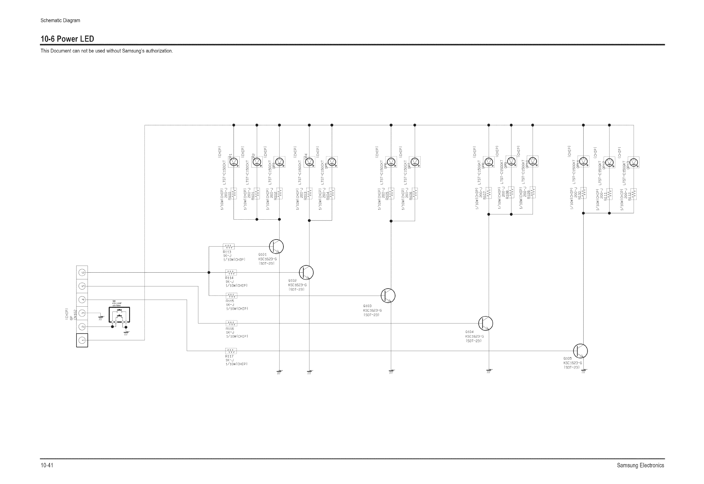
Schematic Diagram
10-6 Power LED
This Document can not be used without Samsung's authorization.
Ri_4
iK d
_/_0W(CHIP)
.......................................................i:'w_i
All5
IK-d
1/i0W(CHZP)
AS _6
IK-J
_/_OW(CHIP)
Aii7
1K d
_/IOW[CHIP)
Q_02 (_
KSC_623 G
(SO[ 23/
Of 03
r_ clH Lr¢<
zesq:
( ) Cd rT
E
)
zoO:
KSC_B23-G
ISOT-23) <
Qt04
KSC623G
(SOT 23)
)
E
Q105 _
KSCSB23G
(SOT-23)
E
Y
B
5
_$.4<
s-©._ <
)
(J
_ >
ocq
<
10-41 SamsungElectr0nics

Schematic Diagram
10-7 RMC
This Document can not be used without Samsung's authorization.
f
,,_ , J
_',:I0 / i]_
!
///
t
£) V
I !
/ / / ///
,i
,i
,i
,i
i
i f:-i-/:_,, v/f:-
i
i
i
SamsungElectronics 10-42

Operation Instruction & Installation
11.Operation Instruction & Installation
11-1Product Features and Functions
11-1-1 Right side buttons
The buttonson the rightside panelcontrolyourTV's basicfeatures,includingthe on-screenmenusystem.
Touse the moreadvancedfeatures,you must usethe remotecontrol.
Press to switch between viewing TV programs and signals from connected components.
Press to see the on-screen menu.
Press to raiseor lower the volume and to select items when using the on-screen menu.
Press to change channels and move between items on the on-screen menu.
Press to activate (or change) a particular item.
11-1-2 Side Panel Jacks
Usethe rightside paneljacks to connecta componentthat is usedonly occasionally(a camcorderor videogame,for example).
Connectthe video signal from a camcorder or video game.
Connectthe audio signal from a camcorder or video game.
Connect an S-Video signal from a camcorder orvideo game.
(S-Video3 jack and Audio L/R input 3 are used in conjunction.)
SamsungElectronics 1I-1

Operation Instruction & Installation
11-1-3 Front Panel LED Indicators
The threelightsonthe frontpanelindicatethe statusof yourTV.
jJ
J
POWER
.............. i Pressto turntheTVonandoff.
"°'°'oo. @ _ Remote Control Sensor
Aimthe remotecontroltowardsthisspoton theTV.
Indicator Light Key
• : Lightis On
(D : Lightis Blinking
(:) : Lightis Off
TIMER LAMP
(:) (D
• (D
(D (:)
(:) (D
(D (D
STANDBY/TEMP .............. Indication
• Standbystate.
(_ The picturewill automaticallyappearin about 15seconds.
Auto TimerON/OFFhasbeensetandthe setwill automaticallybe turnedon in about
( _ 25 seconds.
(D A coolingfan insidethe set is not operatingnormally.
(D Lampcoveronthe rearof the setis not properlyshut.
Checkif the ventilationholeon the rearof the setis blocked,becauseif the inner
(D temperatureis too high, the powerwill shutoff.
(D Lampmaybe defective.
• Ittakes about30secondsfor the TV to warmup, so normalbrightnessmaynot appearimmediately.
• The TV hasa fan to keepthe insidelampfromoverheating.You'lloccasionallyhearit working.
1I-2 SamsungElectronics

Operation Instruction & Installation
11-1-4 Rear Panel Jacks
Usethe rearpaneljacks to connectcomponentssuchas a VCR. Youcan connectdifferentcomponentssuchas VCRs,Set-Top
Box anda DVDplayeretc., becausethereare twosetsof videoinputjacks and twosetsof componentvideoinputjackson the
rearpanelof yourTV.For moreinformation,see "Connections".
1 ANTENNA terminals
Twoindependentcablesor antennascanbe connectedto
theseterminals.Use"ANT1 IN(CABLE)"and"ANT 2 IN(AIR)"
terminalsto receivea signalfromVHF/UHFantennasor your
cablesystem.
2 S-VIDEO INPUT jacks
Connectsan S-Videosignalfrom an S-VHSVCRor DVDplayer.
3 VIDEO/AUDIO INPUT jacks
Connectvideo/audiosignalsfrom externalsources,suchas VCR
or DVDplayers.
4 VIDEO/AUDIO OUTPUT jacks
Sendsvideo/audiosignalsfromthe TVto anexternalsource,
suchas a VCR.Thesejacks are availableonly in RE Videoand
S-Videomodes.
6
7
8
9
10
COMPONENT1, 2 jacks (Y, PB,PR,AUDIO L/R)
Usethesejacks to connectthe componentvideo/audiosignals
froma DVDplayeror a Set-TopBox.
SUB-WOOFER OUT jack
Connectto an active SUB-WOOFER.
PC AUDIO INPUT jacks
Connecttheseto the audiooutputjacks on your PC.
HDMI 2/DVl IN (AUDIO L/R)
Connectto the DVl audiooutputjackof anexternaldevice.
Anynet
Pleasereferto the AnynetOwner'sInstruction.Thisjack is for
connectingto otherSamsungAnynet-enableddevices.
RS232C
Connectto a computerfor readingand loadingdatainformation.
11 DIGITAL AUDIO OUT (OPTICAL) jack
Connectto a DigitalAudioComponent.
12 PC VIDEO INPUT jack
Connecttheseto the videooutputjack onyour PC.
13 HDMI (High Definition Multimedia Interface)/
DVl INPUT jack (HDMI IN 2/DVl IN)
Connectto the HDMIjack of a devicewith HDMIoutput.
Theseinputscan also beusedas a DVlconnectionwithseparate
analogaudio inputs.An optionalHDMI/DVlcablewill be
necessaryto make thisconnection.When usingthe optional
HDMI/DVladapter,the DVlanalogaudio inputson your TVallow
you to receiveleft and rightaudio from your DVldevice.(Not
compatiblewith PC)
14 HDMI (High Definition Multimedia Interface)
INPUT jacks (HDMI IN 1)
Connectto the HDMIjack of a devicewith HDMIoutput.
(NotcompatiblewithPC)
15 D-Net (IEEE1394) S400 MPEG
Connectto externalIEEE1394digital productssuchas digital
VCRsand camcorders.Twojacks areprovidedfor this purpose,
whichallowfor a highdegreeof flexibilityfor connectingyour
D-Netcontrolledsystem.
16 SERVICE
Thisjack is for softwareupgrades.
17 CableCARD TM
Insertthe CableCARDintotheslot.
18 G-LINK TM
Connectthe IRcontrollercabletothe G-LINKTM terminalon your TV.
SamsungElectronics 1I-3
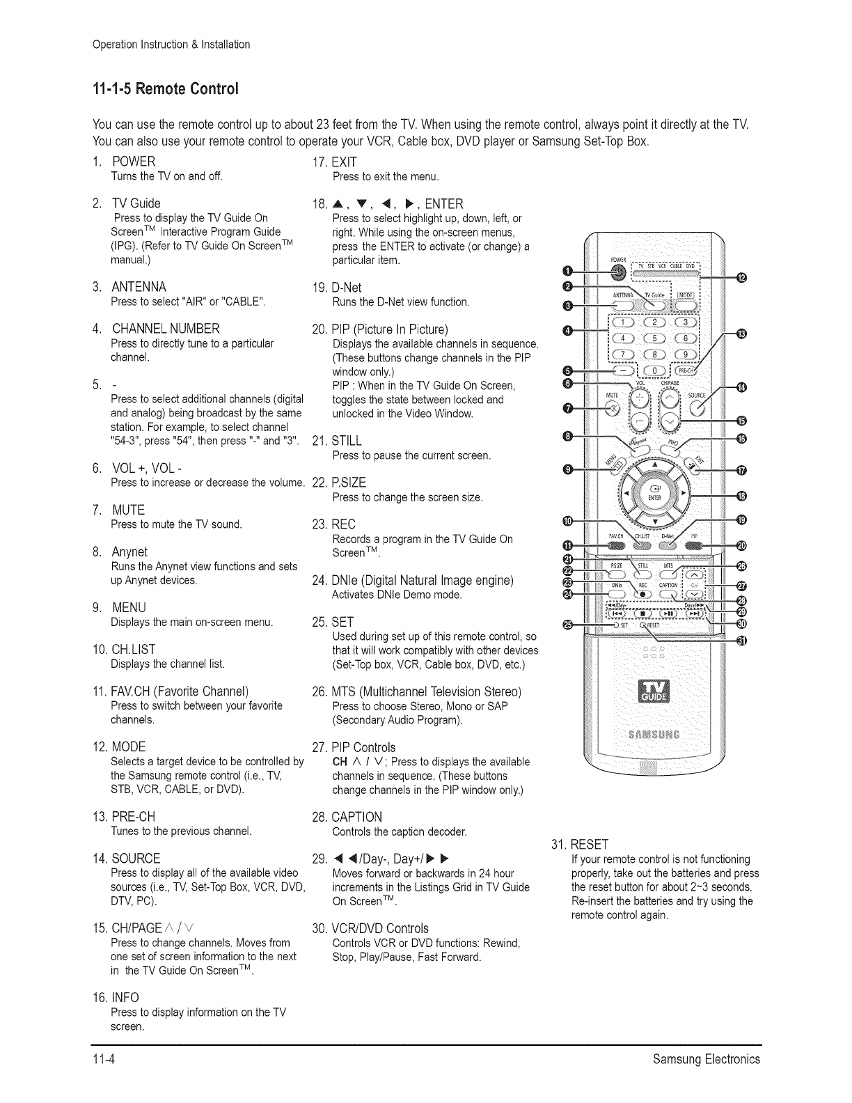
Operation Instruction & Installation
11-1-5 Remote Control
Youcan use the remotecontrolupto about23feetfrom theTV.Whenusingthe remotecontrol,alwayspointit directlyat the TV.
Youcan also useyour remotecontrolto operateyourVCR,Cablebox, DVDplayeror SamsungSet-TopBox.
1. POWER 17. EXIT
Turns the TV on and off. Press to exit the menu.
2, TV Guide 18.
Press to display the TV Guide On
Screen TM Interactive Program Guide
(IPG). (Refer to TV Guide On Screen TM
manual.)
3, ANTENNA 19,
Pressto select"AIR"or "CABLE".
A, T, 4, t_, ENTER
Press to select highlight up, down, left, or
right. While using the on-screen menus,
press the ENTER to activate (or change) a
particular item.
D-Net
RunstheD-Netviewfunction.
4. CHANNELNUMBER
Press to directly tune to a particular
channel.
,
Press to select additional channels (digital
and analog) being broadcast by the same
station. For example, to select channel
"54-3", press "54", then press "-" and "3".
20.
21.
6, VOL+,VOL-
Press to increase or decrease the volume. 22.
7. MUTE
Press to mute the TV sound. 23.
8. Anynet
RunstheAnynetviewfunctionsand sets
upAnynetdevices. 24,
9, MENU
Displaysthe mainon-screenmenu. 25,
10.CH.LIST
Displays the channel list.
26.
11.FAV.CH(FavoriteChannel)
Press to switch between your favorite
channels.
12.MODE
Selects a target device to be controlled by
the Samsung remote control (i.e., TV,
STB, VCR, CABLE, or DVD).
13.PRE-CH
Tunes to the previous channel.
14.SOURCE
Press to display all of the available video
sources (i.e., TV, Set-Top Box, VCR, DVD,
DTV, PC).
15.CH/PAGEA /v
Press to change channels. Moves from
one set of screen information to the next
in the TV Guide On ScreenTM.
PIP(PictureIn Picture)
Displays the available channels in sequence.
(These buttons change channels in the PIP
window only.)
PIP : When in the TV Guide On Screen,
toggles the state between locked and
unlocked in the Video Window.
STILL
Press to pause the current screen.
P.SIZE
Press to change the screen size.
REC
Records a program in the TV Guide On
ScreenTM.
DNle (Digital Natural Image engine)
ActivatesDNle Demomode.
SET
Used during set up of this remote control, so
that it will work compatibly with other devices
(Set-Top box, VCR, Cable box, DVD, etc.)
MTS (Multichannel Television Stereo)
Pressto chooseStereo,Monoor SAP
(SecondaryAudio Program).
27.
28.
29.
PIP Controls
CH A /V; Pressto displaystheavailable
channelsin sequence.(Thesebuttons
changechannelsin the PIPwindowonly.)
CAPTION
Controlsthecaptiondecoder.
4 4/Day-, Day+/i_ 1_
Moves forward or backwards in 24 hour
increments in the Listings Grid in TV Guide
On ScreenTM.
% VCR/DVD Controls
ControlsVCR or DVDfunctions:Rewind,
Stop,Play/Pause,Fast Forward.
.............................. ..................
31. RESET
If your remote control is not functioning
properly, take out the batteries and press
the reset button for about 2-3 seconds.
Re-insert the batteries and try using the
remote control again.
16.INFO
Press to display information on the TV
screen.
1I-4 SamsungElectronics
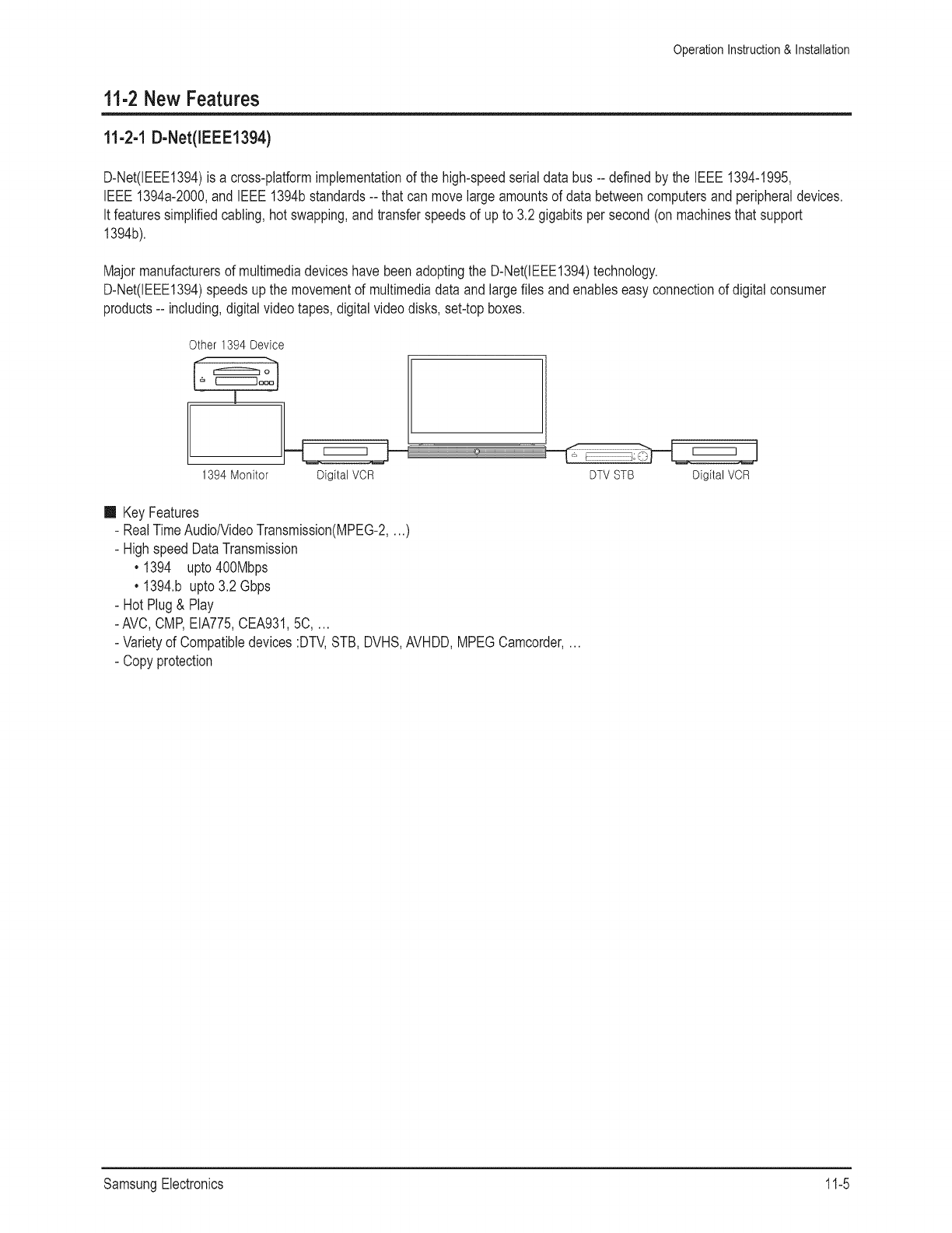
Operation Instruction & Installation
11-2 New Features
11-2-1 D-Net(IEEE1394)
D-Net(IEEE1394)is a cross-platformimplementationof the high-speedserialdatabus -- definedby the IEEE1394-1995,
IEEE 1394a-2000,andIEEE 1394bstandards-- thatcan movelargeamountsof data betweencomputersand peripheraldevices.
It featuressimplifiedcabling,hotswapping,andtransferspeedsof upto 3.2 gigabitspersecond(onmachinesthatsupport
1394b).
Majormanufacturersof multimediadeviceshavebeenadoptingthe D-Net(IEEE1394)technology.
D-Net(IEEE1394)speedsupthe movementof multimediadata andlargefiles andenableseasyconnectionof digitalconsumer
products-- including,digitalvideotapes,digitalvideodisks,set-topboxes.
Other 1394 Device
I
1394 Monitor Digital VCR
Im Key Features
- RealTimeAudio/VideoTransmission(MPEG-2.... )
- HighspeedDataTransmission
• 1394 upto400Mbps
• 1394.b upto3.2 Gbps
- Hot Plug& Play
-AVC, CMP,EIA775,CEA931,5C....
- Varietyof Compatibledevices:DTV,STB,DVHS,AVHDD,MPEGCamcorder....
- Copyprotection
DTV STB Digital VCR
SamsungElectronics 1I-5

Operation Instruction & Installation
11-2-2 TV Guide On Screen
TV GuideOnScreenis an interactiveprogramguidethatis builtdirectlyintoconsumerelectronicsproducts,includingDLP,
plasmaand LCDtelevisions,personalvideorecordersand recordableDVDplayers.
The guideoffersinteractiveon-screenprogramlistingsthatenableviewersto quicklyand
easilynavigate,sort, select,andscheduletelevisionprogrammingfor viewingandrecording,
allwith simpleremotecontrolcommands.
TV GuideOnScreen'spatentedtechnologydeliverscontinuouslyupdatedprogramlistingsto
users,regardlessof whethertheyreceivetheirtelevisionsignalvia cableorover-the-air
broadcast.TV GuideOn Screenworksby simplyplugginginthe televisionor recording
deviceandactivatingthe guidethroughan expressset-upprocess.
The guiderequiresnosubscriptionor specialconnectionand is availableat no costto theconsumer.
II Key Features
- ListingsService:
Displayseightdaysof viewers'local programlistingsanddescriptionsfor broadcastandcable;
Viewerscan tuneto anyprogram,schedulea programto record,orset a reminder,with the pressof a button;
The VideoWindowletsviewersmonitorthe lastchanneltunedwhileviewingprogramlistings,or previewchannelsas they
pagethroughlistings;
Color-codedprogramgenreshelpviewersquicklyidentifymovies,sports,and children'sprogramming.
- SearchFeature:
Viewerscan searchfor programsby categoriessuchas HDTV,movies,sportsor children'sshows.Withincategories,viewers
can sort by showtype,suchas baseballorfootball.
Viewerscan sortalphabetically,or by a keywordsuchas a showtitleor a starringactor.
- One-touchRecording:
To record,viewerssimplyhighlighta programtitleandthen pressa buttononthe remotecontrol.TV GuideOn Screenwill
automaticallyrecordthe program;
Programsmaybeset to recordonetimeor everytimetheyair;
TV GuideOnScreenis a criticalcomponentof the recordabledevicesintowhichit is built.A week'sworthof listingsand
powerfulsortingand recordingfeaturesmakeadvancedrecordingsimple
- ReminderFeature:
Viewersmayset remindersto ensurethey nevermisstheirfavoriteshows;
Reminderscaneven beset to automaticallyturn on theTV whena showbegins.
11-2-3 CableCARD
Asmall PCMCIAdevice,notworkingby itself,designedto runspecializedtasksinassociationwith a DCRTV,suchas a
conditionalaccesssubsystemor to provideresourcesrequiredby anapplicationbut not provideddirectlybythe host.
1I-6 SamsungElectronics

Operation Instruction & Installation
11-2-4 RS-232C
DLPDTUusingtheserie|port.
Settings(SdectStandardRS232}
19200 bps
b_s
None
b_t
Configuration
Since AnyneL GLink and RS232C share a seriat port, you have to
co_ecl_RS232C from _e menu _r the fo_lowing cororourdcetion.
Menu Setting Procedures
Se_ct Setup _ Port Selection _ RS232C
Protocot
A command packet o'ansists of 7 bytes in total,
The two bytes 0){08 and 0_:22_atly thatthe gacksiis for serial cr_nmt_iCatba.
The fol_i_ 4 b)tes rapm"_ a/m_f_ o_mrrar_tha_ be defir_ s,_tf_ _
The last by¢e8 the d'_ecl,ata'nwhic,h ches_ksthe ,_a4iditfof the cornealp_kat
Header [2 Byte]: Pre_definad values fixed _o0x0_ and 0x22
Cm_l [1 Byte]: Thefirst value of the _:odedefined in the c_ list(He.alm!!)
Cmd_If Byte]: The s_ v_ d_ _ defi_ h _'_com_ _st (He×_)
Cmd3 [1 B/tel: Thethird value of the C_e defin_ h the command _ist(Heyadedmal)
Va[_ I1 Byte]: _n#ut_m#etef for the _mm_d (_fault: 0) (H_dmal)
BS [1 Byte]: Checksum{theZs oum_t_mer_of the sumd_t t_ values_t fat_heCB vs!_,)
Sequence
PC
Creates a command pack_et and co_ds it through RS2_2C
'_ BLP DTv'
Receives a packe_ and parses t_ packeL
Detetroir_es whether if is a sucttess or fai. aRd frar_sroits _he Ask p_ket to the PC,
Controls _ DLP DTV with the parsed cororoaad,
{ PC
Waits for the Ask packs&
Prepares the next ceroroaad_ if a Success packet arrives iro_d_ately.
Success _ Fail
When the received pacer from an seternai de,.nde _as a valid
value a Sagas packet is _, Otherw_e, a Fail packet is sen_
AFai_ packet ia ae_t if:
'_ The r_ived/_t _engthis r_l equal to 7bytes.
_s 2 L54epackel _d_ vaJ_ is not equatto 0_8, 0×22,
The check sum is inoron'_t
Fail_s da_a_io_ by sa external device
An external devi_ d&ssifies the packet as Fa{I if it does not receive
a Scoeees packet wtthin 100mS,
SamsungElectronics 1I-7

Disassembly & Reassembly
12. Disassembly & Reassembly
12.1OverallDisassembly& Reassembly
12-1-1 Separation of the back cover and the chassis
PartName Description Description Photo
Back Remove 12 screws to remove the back bottom cover.
Cover : TH,B,M4.L15,BLK,SWRCH18A
Terminal Remove 5 screws to remove the Terminal Board.
Board
* The 3 Terminal Board Screws
TH,B,M4.L15,BLK,SWRCH18A
* The 3 Jack Screws
" RH,B,M4,L15,ZPC(BLK),SWRCH18
DVI cable Separate the DVI cable.
:The DVI screw is made of soft plastic and may easily
break when applying excessive force through a screw driver.
Ensure that extreme caution is taken when loosening the screw.
SamsungElectronics 12-1
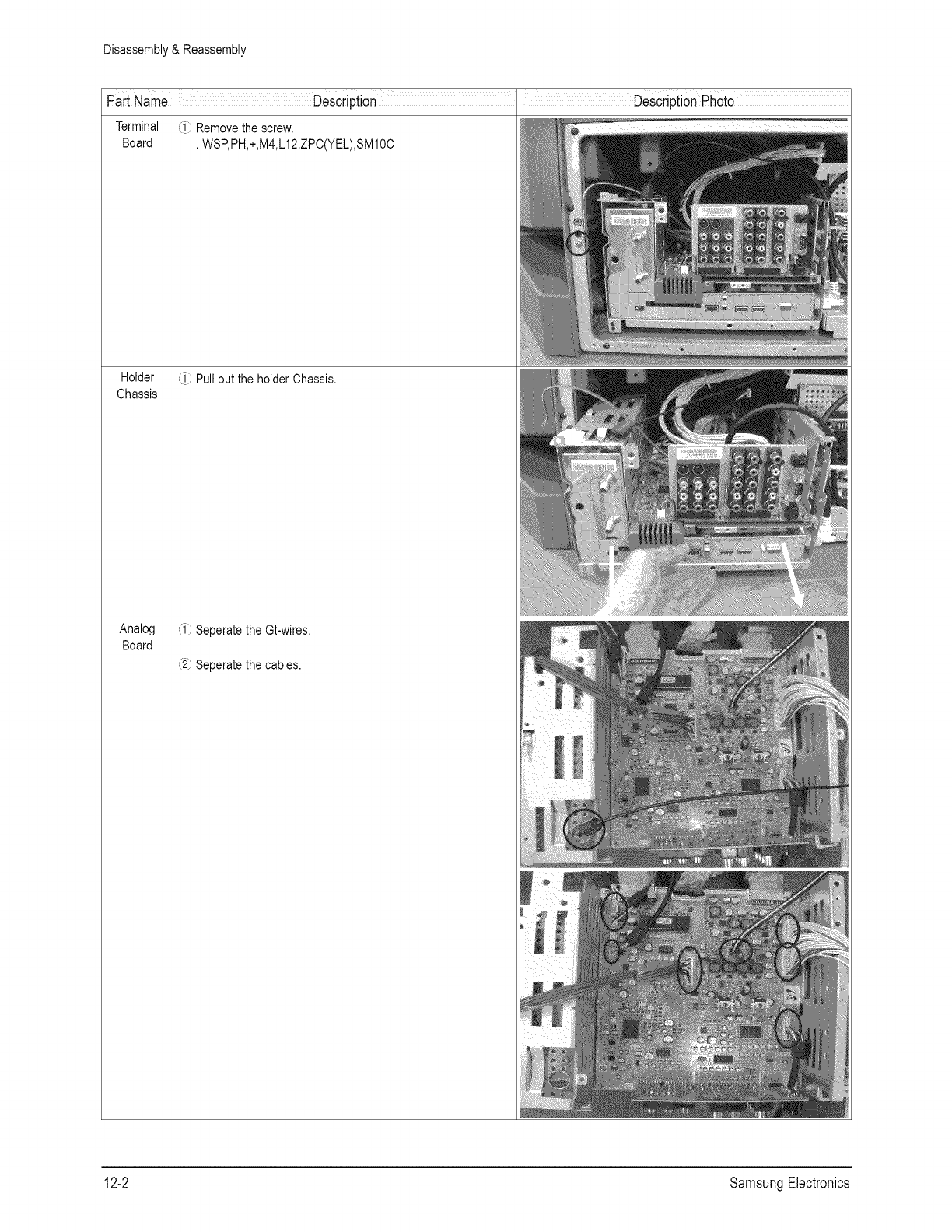
Disassembly & Reassembly
Part Name
Terminal
Board
Holder
Chassis
Analog
Board
(_ Remove the screw.
: WSP,PH,+,M4,L12,ZPC(YEL),SM10C
(_ Pull out the holder Chassis.
Seperate the Gt-wires.
!iiii__¸ii_iiii:_
,% Seperate the cables.
12-2 SamsungElectronics
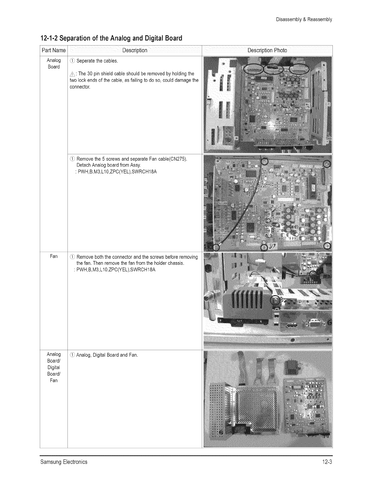
Disassembly & Reassembly
Analog
Board
12-1-2 Separation of the Analog and Digital Board
PartName' Description I DescriptionPhoto
Seperate the cables•
Fan
Analog
Board/
Digital
Board/
Fan
!Q: The 30 pin shield cable should be removed by holding the
two lock ends of the cable, as failing to do so, could damage the
connector•
,_1 Remove the 5 screws and separate Fan cable(CN275).
Detach Analog board from Assy.
• PWH,B,M3,L10,ZPC(YEL),SWROH18A
Remove both the connector and the screws before removing
the fan. Then remove the fan from the holder chassis•
• PWH,B,M3,L10,ZPC(YEL),SWROH18A
Analog, Digital Board and Fan.
SamsungElectronics 12-3

Disassembly & Reassembly
Part Name
Digital
Board
Description I DescriptionPhoto
(_ Use the long-nosed pliers to remove the hex nut.
Nut-Hexagon : -,M3/8X32,ZPC(WHT),MBSBD
J.,\: The standoffs can easily break if excessive force is applied.
Use extreme caution when removing and replacing.
(_ Remove 2 standoffs from the DVI connector.
StandOff : M3,L5,Ni PLT,SUM24L,#4-40
:2) Remove 2 standoffs from the PC connector.
(_ Remove the screws and cables.
: PWH,B,M3,L10,ZPC(YEL),SWRCH18A
/,\: The 30 pin shield cable should be removed by holding the
two lock ends of the cable, as failing to do so, could damage the
connector.
(_ After Removing the Top Shield Case.
/,\: Use the two lock holes on either side of the shield case
when removing it.
12-4 SamsungElectronics
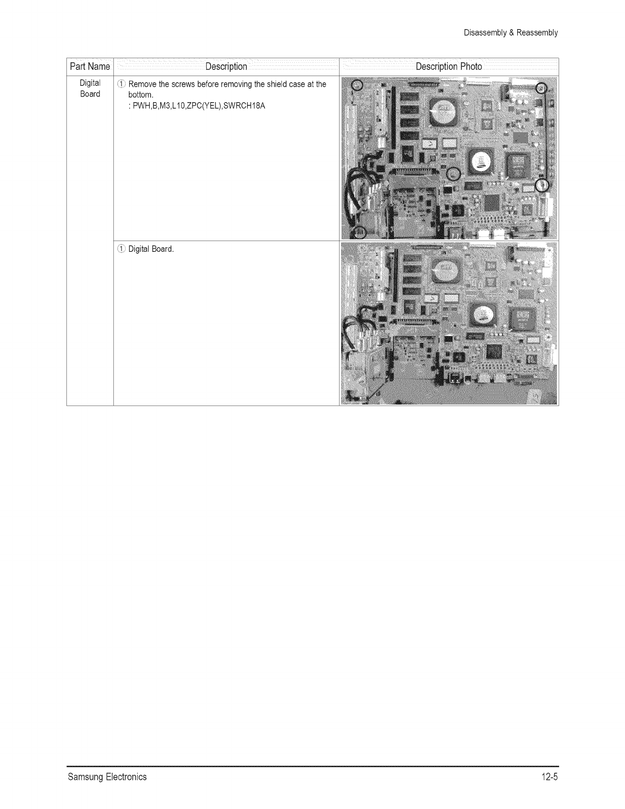
Disassembly & Reassembly
Part Name
Digital
Board (_ Removethe screwsbeforeremovingthe shieldcase at the
bottom.
: PWH,B,M3,L10,ZPC(YEL),SWROH18A
(_ Digital Board.
SamsungElectronics 12-5
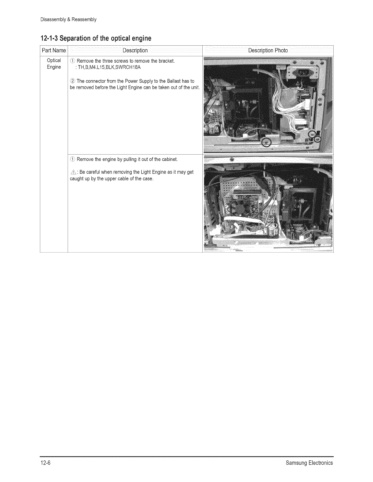
Disassembly & Reassembly
12-1-3 Separation of the optical engine
PartName' Description DeScriptionPhoto
Optical (_ Remove the three screws to remove the bracket.
Engine :TH,B,M4.L15,BLK,SWRCH 18A
:2 The connector from the Power Supply to the Ballast has to
be removed before the Light Engine can be taken out of the unit.
(_ Remove the engine by pulling it out of the cabinet.
jR: Be careful when removing the Light Engine as it may get
caught up by the upper cable of the case.
12-6 SamsungElectronics

Disassembly & Reassembly
12-1-4 Separation of the Power Board
Part Name
Power
Board Separate the cables.
Remove the power board carefully before disconnecting the
cables.
Notice: Wear gloves when handling the power board as
there may be some remaining electrical charge in the capacitors.
Specifically, avoid touching any part of the capacitors.
Afterremovingthe screws,separatethe bottompowerbraket.
•PWH,B,M3,L10,ZPC(YEL),SWROH18A
i iiii i iiii! !!!ii!i!!ii!i!
SamsungElectronics 12-7

Disassembly & Reassembly
12-1-5 Screen Remove
Part Name
Cover-Front
Brkt-
Screen ,Top
/
Brkt-
Screen,
Right
Screen
,_1Cover-Front'slower departmentpullto fore-endand remove.
J.,\,:There is noScrewconclusionplace.
State that Cover-Front is detached.
Separate Brkt-Screen,Top and Right after remove 6 screws
indicating in picture.
:TH M4,L12,YELLOW.
,_1 Separate Screen.
12-8 SamsungElectronics

Disassembly & Reassembly
12-1-6 Lamp Replacement
/.,\ Notice
1. Replacewith the correctcode numberedlampto avoiddamageto the TV.
2. Turnthe poweroffandwaitfor 30minutesbeforereplacingthe lampas it will be hot.
3. Donot touchtheglasspart of the lampwithyour barehandsnorinsertany foreignobjectinsidethe coveras it maycausepoor
screenquality,electricshockor fire.
4. Do not placethe old lampnearflammableobjectsor withinthe reachof children.
5. Besureto connectthisTV directlyto anAC wall outlet. Ifthe TV'sAC plugis connectedto a cable boxor othersource,it will
not allowfor propercool downtime.
Part Name Description DescriptionPhoto
Lamp Unplug the TV, then use a screwdriver to remove the 4
screws.
•WSP,PH,+,M4,L12,ZPC(YEL),SM10C
Remove the Lamp cover•
Loosen the screw securing the Lamp by using a screwdriver•
• WSP,PH,+,M4,L12,ZPC(YEL),SM10C
...........
}
SamsungElectronics 12-9
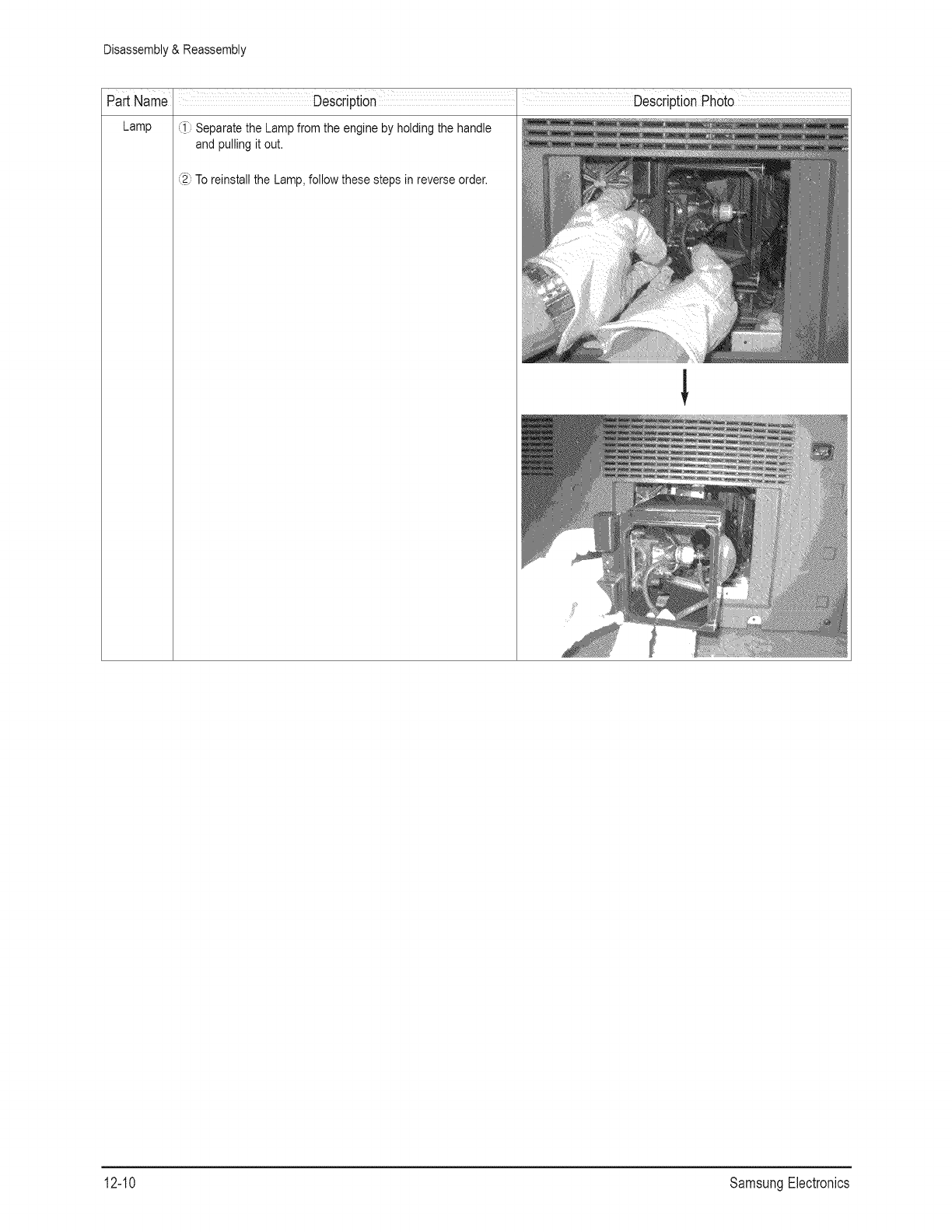
Disassembly & Reassembly
Part Name
Lamp (_ Separate the Lamp from the engine by holding the handle
and pulling it out.
% To reinstall the Lamp, follow these steps in reverse order.
12-10 SamsungElectronics

Disassembly & Reassembly
12-1-7 Ballast Replacement
Part Name
Ballast
Board (_ Remove the lamp, refering to lamp replacement.(12-8page)
Remove the ballast power cable.
(_ Remove the Ballast SCI cable.
(_ Removethe twoscrewsat the HolderBallast.
: PWH,+,B,M3,L10,ZPC(YEL),SWROH18A,-
(_ Pull out the Ballast assembly.
% Replace it with a new one and re-assemble it in the reverse
order.
SamsungElectronics 12-11
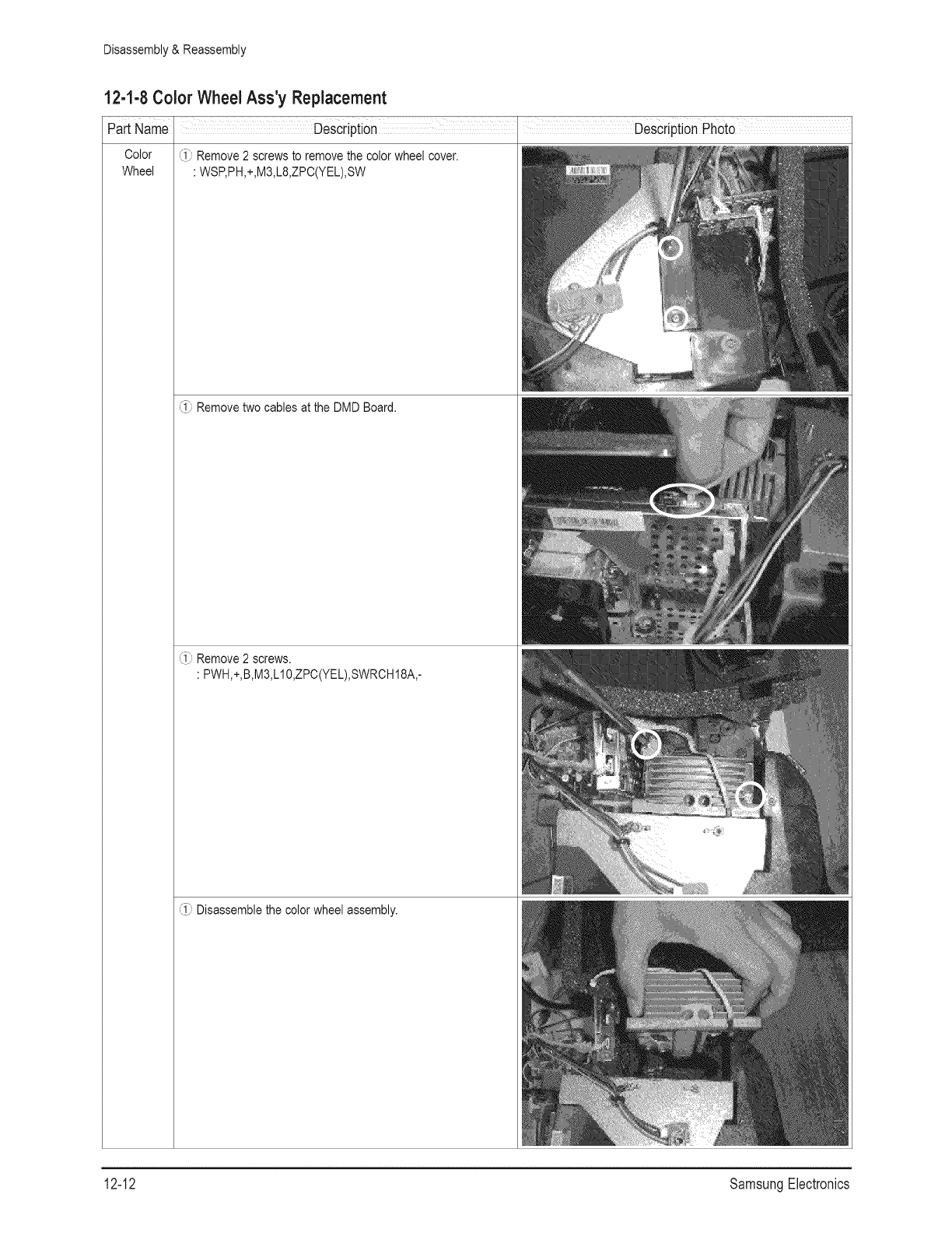
Disassembly & Reassembly
12-1-8 Color Wheel Ass'y Replacement
Part Name
Color
Wheel
,_1Remove2 screwsto removethe colorwheel cover•
: WSP,PH,+,M3,L8,ZPC(YEL),SW
Remove two cables at the DMD Board•
Remove 2 screws•
• PWH,+,B,M3,L10,ZPC(YEL),SWRCH18A,-
Disassemble the color wheel assembly•
12-12 SamsungElectronics
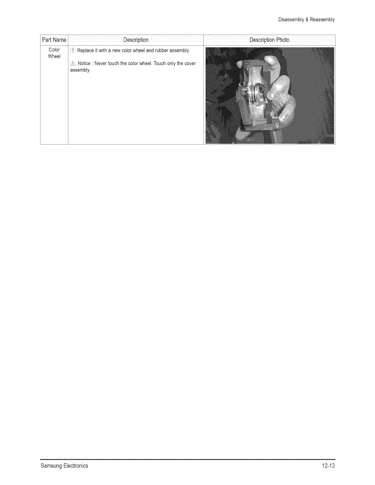
Disassembly & Reassembly
Part Name
Color
Wheel ,_1 Replace it with a new color wheel and rubber assembly.
Notice • Never touch the color wheel. Touch only the cover
assembly.
SamsungElectronics 12-13

Disassembly & Reassembly
12-1-9 Actuator(Smooth Picture) Replacement
PartName
Actuator (i Remove the cable at the Actuator.
(i Remove screws(3ea) at the Actuator cover.
: BH,+,M3,L16,ZPC(YEL),SWROH
(i Replace it with a new actuator.
12-14 SamsungElectronics

Disassembly & Reassembly
12-1-10 Dynamic Black Replacement
i
PartName Description DescriptionPhoto
Remove the at the cable.Dynamic
Black
(_ Remove screw(2ea).
: WSP,BH,+,M3,L16,ZPC(YEL),SWRCH
(i Disassembly Dynamic Black assembly.
(i Replace it with new Dynamic Black assembly.
SamsungElectronics 12-15
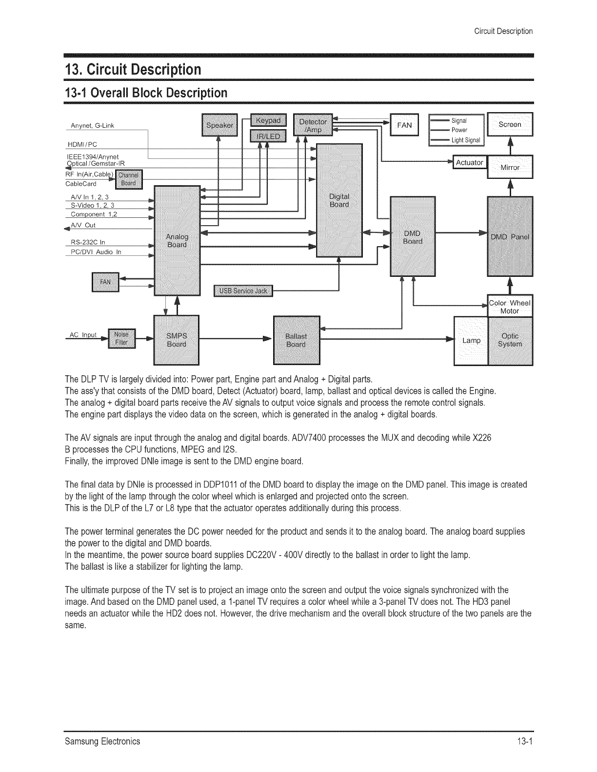
Circuit Description
13. Circuit Description
13-1 Overall Block Description
Anynet, G-Link
HDMI/PC
IEEE1394/Anynet
Optical/Gemstar-IR
RF In(Air,Cabl_
CableCard
AlVIn 1,2,3
S-Video 1 2 3
Component 1,2
,,_A/V Out
RS-232C In
PC/DVI Audio In
'_E_ [_ Signal
Power
Light Signal
AC
The DLPTV is largelydividedinto:Powerpart,Enginepart andAnalog+ Digitalparts.
The ass'ythat consistsof the DMD board,Detect(Actuator)board,lamp,ballastand opticaldevicesis calledthe Engine.
The analog+ digitalboardpartsreceivetheAVsignalsto outputvoicesignalsandprocessthe remotecontrolsignals.
The enginepartdisplaysthe videodata on the screen,whichis generatedin the analog+digital boards.
TheAVsignalsare inputthroughthe analoganddigitalboards.ADV7400processesthe MUXanddecodingwhile X226
B processesthe CPUfunctions,MPEGand12S.
Finally,the improvedDNleimageis sentto the DMDengineboard.
Thefinal data by DNleis processedin DDP1011of the DMDboardto displaythe imageonthe DMD panel.Thisimageis created
by the lightof the lampthroughthe colorwheelwhichis enlargedandprojectedonto the screen.
Thisis the DLPof the L7 or L8typethatthe actuatoroperatesadditionallyduringthis process.
The powerterminalgeneratesthe DC powerneededfor the productandsendsit to the analogboard.The analogboardsupplies
the powerto the digitalandDMD boards.
In the meantime,the powersourceboardsuppliesDC220V- 400Vdirectlyto the ballastin orderto light the lamp.
The ballastis like a stabilizerfor lightingthe lamp.
The ultimatepurposeof the TV set is to projectan imageontothe screenand outputthe voicesignalssynchronizedwiththe
image.And basedonthe DMDpanelused,a 1-panelTV requiresa color wheelwhile a 3-panelTV doesnot.The HD3panel
needsanactuatorwhile the HD2doesnot. However,the drivemechanismand the overallblockstructureof the two panelsare the
same.
SamsungElectronics 13-1
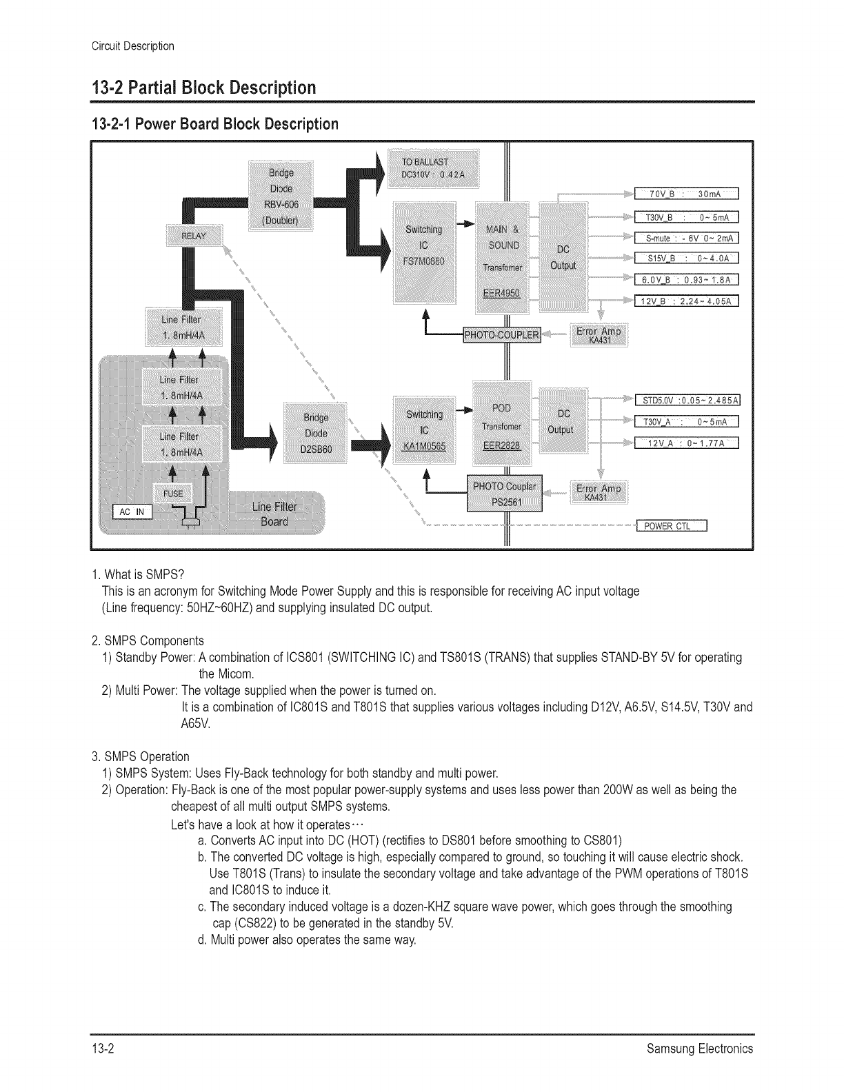
Circuit Description
13-2 Partial Block Description
13-2-1 Power Board Block Description
tI
30mA ]
T30V_B : 0 _ 5mA J
s=mute : = 6V 0 ~ 2rnA ]
: 0~ 410A
6=0V B : 0=93 ~ 1=8A ]
12V B : 2.24~4.05A ]
STD5=0V 10.05 ~ 2=485A[
T30V A : 0 _5mA I
A : 0 _-1.77A ]
[ POWER CTL ]
1.Whatis SMPS?
This is anacronymfor SwitchingModePowerSupplyand thisis responsiblefor receivingAC inputvoltage
(Linefrequency:50HZ~60HZ)andsupplyinginsulatedDCoutput.
2. SMPSComponents
1) StandbyPower:A combinationof ICS801(SWITCHINGIC)andTS801S(TRANS)that suppliesSTAND-BY5Vfor operating
the Micom.
2) MultiPower:The voltagesuppliedwhen the poweris turnedon.
Itis a combinationof IC801SandT801Sthat suppliesvariousvoltagesincludingD12V,A6.5V,$14.5V,T30Vand
A65V.
3. SMPSOperation
1) SMPSSystem:UsesFly-Backtechnologyfor both standbyandmultipower.
2) Operation:Fly-Backis oneof the mostpopularpower-supplysystemsand useslesspowerthan 200Was wellas beingthe
cheapestof all multioutputSMPSsystems.
Let'shavea lookat howit operates...
a. ConvertsAC input intoDO (HOT)(rectifiesto DS801beforesmoothingto CS801)
b. The convertedDCvoltageis high,especiallycomparedto ground,so touchingit will causeelectricshock.
UseT801S(Trans)to insulatethesecondaryvoltageandtakeadvantageof the PWMoperationsof T801S
and IC801Sto induceit.
c. Thesecondaryinducedvoltageis a dozen-KHZsquarewavepower,whichgoesthroughthe smoothing
cap (CS822)to begeneratedin the standby5',/.
d. Multipoweralso operatesthe sameway.
13-2 SamsungElectronics

Circuit Description
4, Input&Outputvoltage
1) Inputvoltage * Aemrica(AC120V)-OPTION
• Korea(AC220V)-OPTION
• The others(ACl00V~AC240V)- OPTION
2) Outputvoltage * D12V/2,5A- 12V, 3,3V, 1,8V: For signalprocessing
• A6.5V/1A- Fordrivingthetuner
• $14.5V/4A-For drivingsound processor
• T30V/5mA- Fordrivingthe tuner
• A65V/30mA- Fordrivingthe actuator
SamsungElectronics 13-3
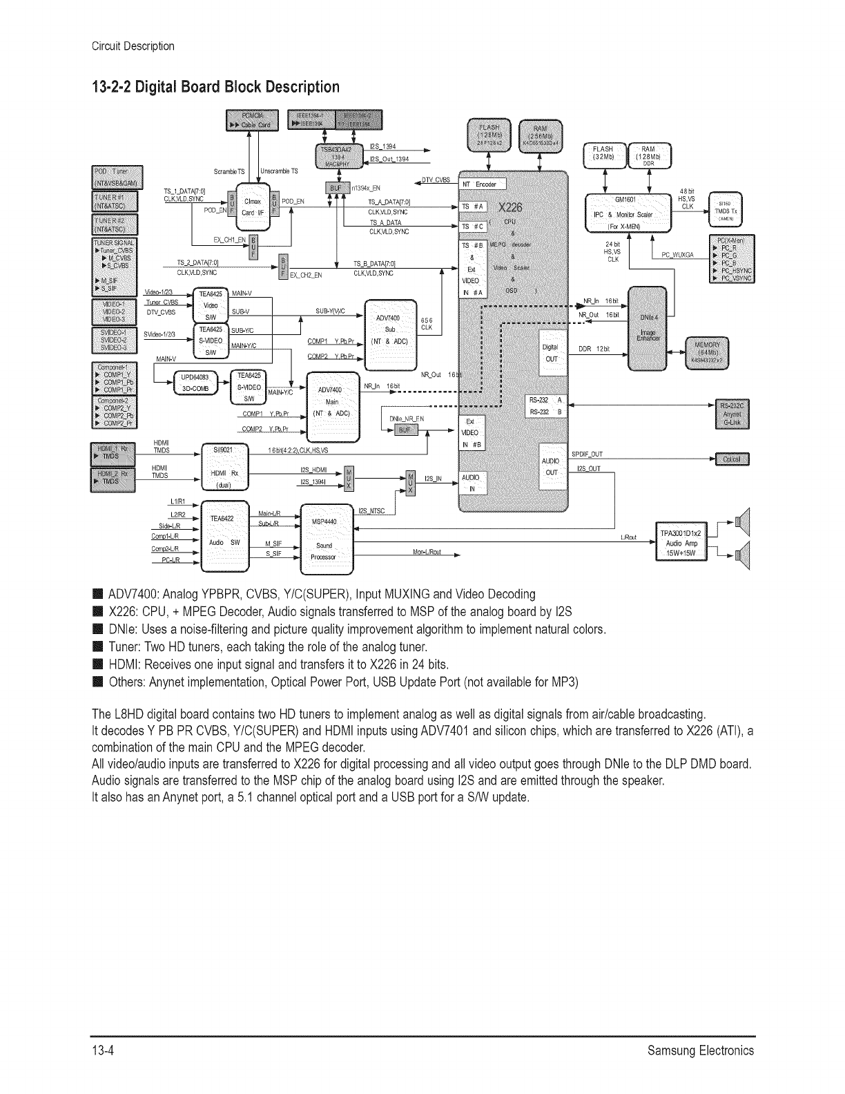
Circuit Description
13-2-2 Digital Board Block Description
ScrambleTS Unscramble TS
POD _N
TS_2_DATA[7:O] _.___ __
CLK,VLD,SYNC EX CH2 EN
MAIN-V
COMP1
COMP1
COMP2
HDMI
HDMI 12S_HDMI
TMDS 12S_13941
L1/R1
L2tR2
Side-L/R
12S_1394
12S_Out_1394
,_1394×sN
TS_A_DATA[f:0]
CLK,VLD,SYNC
TS A DATA
CLK,VLD,SYNC
TS_B_DATA[/:0l
CLK,VLD,SYNC
NR_Out
NRJn 16bit
DNle NR EN
MomL/Rout
24_t t l
HS,VS PC WUXGA
CLK
NR_Out 16b_t
DDR 12bit
PDIF_OUT
12S_OUT
II ADV7400:AnalogYPBPR,CVBS,Y/C(SUPER),InputMUXlNGandVideoDecoding
II X226: CPU,+ MPEGDecoder,Audiosignalstransferredto MSPof the analogboardby 12S
II DNle:Usesa noise-filteringand picturequalityimprovementalgorithmto implementnaturalcolors.
II Tuner:TwoHDtuners,eachtakingthe roleof the analogtuner.
II HDMI:Receivesone inputsignalandtransfersit to X226in 24 bits.
II Others:Anynetimplementation,OpticalPowerPort,USBUpdatePort (notavailablefor MP3)
The L8HDdigitalboardcontainstwo HDtunersto implementanalogas well as digitalsignalsfromair/cablebroadcasting.
It decodesY PBPR CVBS,Y/C(SUPER)and HDMIinputsusingADV7401andsiliconchips,whicharetransferredto X226(ATI),a
combinationof the mainCPUandthe MPEGdecoder.
All video/audioinputsare transferredto X226for digitalprocessingandall videooutputgoes throughDNleto the DLP DMDboard.
Audiosignalsare transferredto the MSPchip of the analogboardusing12Sandareemittedthroughthe speaker.
It also hasanAnynetport,a 5.1 channelopticalportand a USBportfor a S/Wupdate.
13-4 SamsungElectronics

Circuit Description
13-2-3 Analog Board Block Description
S1/S2/S3-Y
Sl/S2/S3-C
Comb-Y-Out
Comb-C-Out
MTNR-CVBS
STNR-CVBS
DTV-CVBS
V1/V2
Side-V
Main-Y-Out
Main-C-Out
Sub-YOut
Sub-COut
Side-Y/C
Main-V-Out
Sub-V-Out
Cap:V:Out
MomV-Out
Main-Y(V)-Out
Sub-Y-Out
Sub-C-Out
Cap-Y-Out
Mon-Mixed-V-Out
/
,€
Main-Y(V)
_'_ Main-C
Sub-Y(V)
Sub-C
Cap-CVBS
_,_ Mon-Vout
L1/R1
L2/R2
Side-dR
Compl-L/R
Comp2-dR
PC-dR
Vlain-L/R
MTNR-SIF
STNR-SIF
DVI(HDMt2)-L/R
Mon-L/Rout
Amp-ln-dR
Gain0/Gain1
m AnalogVideoSignalProcessing
m SelectSound/Video
Oneis selectedfrommultipleinputsby the switchingID. MICOMdecideswhichportis usedfor output.
For broadcastingsignals,sub-outputsare transferredin CVBSand,the mainoutputsinY/C throughthe 3D Comb,to the digital
board.
Soundsignalsareselectedby the switchingIC,of whichonly oneinput is transferredto the speaker.
m DetectionSignalFlow
Wheneach port is connectedto asignalcable,the detectionsignalis "low"and can becheckedby Micomscanning.
m Y/C Separation
The 3D CombfilterdividesRFCVBSsignalsintoY/C beforebeingtransferredto the digitalboard.
SamsungElectronics 13-5

Circuit Description
13-2-4 DMD Board Block Description
Lain
Power Good
Reset M
CLKRX
DATRX
- _ DMD C r
- _- Lv B M
- -- ds us aster A/B
---
B ODD "_
........... _ Lvds Bus SLave A/B
i ,on
i Confgura
, EEPROM _ _ r.__._. _._100Mhz
Rambus] J _
LM 393 F
't A89O4p-
--_ Lamp En
-- Lamp Litz
-- CW Index
;et
II Controlsthe lamp(ON/OFF)
II Drivesthe colorwheelmotor
II Drivesthe panel
II Controlsthe sensors
3.3 V output ]
_'1 VCM Actuator
_- I DB Actuator
>/ Detector Circuit
I 24 P con
13-6 SamsungElectronics

Circuit Description
13-3 New Circuit Description
13-3-1 Output Voltage States of the DMD Board Parts
-- 25V
Output Terminal _f-
Waveform for 8V
RA600,601,602,603
26V
LOC Characteristics
BD904 LAMP EN High from DDP1011
BD902 LAMP LITZ High(5V) before the lamp turns on, Low(0V)
when the lamp turns on
13-3-2 DMD Panel Pin Terminal Characteristics Diagram
-_ Removethe heatsinkattachedto the DMD Boardandtightenthe screwsin four placesandthen inspectthe characteristicsof
each pinterminal.
%
ii)_!i
i!!ii_iii!i
P14
NIC
NlC
The vertical lines, which may occur due to improper connections between the panel and the
PCB, occur with interva)s of 50 inches(26mm), if vertica) lines occur with intervals of more than
26mms, it indicates a failure of the DDP1011 (C itself, if they occur with intervals of less than
26mm, it means that more than two pins have bad connections.
[] ;Bi!i
16
i_i:iiiiii
DA,DB output wave
[Screen:WHITE]
P6
ii!i_i)_iii!ii_ii_iiii
)_i!!_!i))
)ii!_
_iiiiii!!i_!!i!i!ii!i!!i_
[]
_iiiiii!!i_!!i!i!ii!i!!i_
m
[] m
[] m
mm
[]
[] []
[]
[] iiiiif_iii
!iiiii)_!i!i!!i!!i)!!)_i!i!i!i!
[]
))))_iiiiii_
[]
!ili;i!iii!i_i!i!ii!i!ii!
[]
[] m
m[]
[] )i!i!ii!iiiii!!l!i!_il!i
m
[]
[]
!!!ii_iii!_ii%il
[] []
[] []
%!i)[]
[] %iiiil
)_!i%
%!;!i
i!iii%
[] []
[] iiii_iii!i
iiiii_ii!il
iiiiii_iiii)!iiiiii_iiiiiiii
!i)ii_)_!iiiiiiiiii;_i!ilSi!!i
N
m
iiil_ii!il
i%!
ii!_i!ii¸
_2
i)!_i!_!!i!i;_ii!i!iii_i_iiii!il;ilili!
ii!i!ii_!ii!i!il¸
))ii_iiiii
%i:)li
))i!_iiiiiii!
Pin Name
V
V2
DA
DB
NO.
G
Description Pin Name Description ........
Voltage : 3.3V T Test Point
VCC2 : 8V ME Mirror Bias Extra
A Channel Data Bus [When measured, there should be a waveform] C Clock
B Channel Data Bus [When measured, there should be a waveform] P# A,B Channel Positive
MBRST# (Mirror Bias Rest) 26V N# A,B Channel Negative
The part from the present position to the GND (The black part is also a GND.)
SamsungElectronics 13-7

Circuit Description
13-3-3 Description of TerminalCharacteristics
Pin Name I Description
SCTRL_BN/P B channelLVDSserial control
DCLK_BN/P B channelLVDSCLOCK
SCPDI SERIALCONTROLDATAINPUT
SCPDO SERIALCONTROLDATAOUTPUT
SCPENB SERIALCONTROLENABLE
SCPCK SERIALCONTROLCLOCK
DMDRESETB DMD LOGICRESET
MBRST(14:0) MIRRORBIASRESET
MBRST_EXTRA UNUSEDMIRRORBIASRESET
SCR_CLR TESTCLEARPINS(NORMALGND)
READOUTA(I:0) A-CHANNELSERIALDATAOUTDURINGSPAMREADTESTOPERATION
READOUTB(I:0) B-CHANNELSERIALDATAOUTDURINGSPAMREADTESTOPERATION
TP(2:0) MANUFACTORINGTESTPOINT(NOCONNECTEDDURINGNORMALCPERATION)
RSV_A(4:0)/RSV_B(4:0)RESERVEDPINS(NORMAL:GND)
EVCC REFERENCEVOLTAGEDURINGSPAMREADTESTOPERATION(NORMALGND)
VCC2 MIRRORELECTRODEVOLTAGE(7,3V)
VCC LOGICSUPPLY
VSS LOGICGROUND
13-3-4 Engine Failure Inspection Flow Chart for the DMD Board
Key Point
Checkwhether the
1)When the power cordis plugged in, DC220W410V(typical300V)
1 2) DC220W410V(typical300V) is automaticallysuppliedto the ballast, power issuppliedto the ballast.
t)
2 Checkwhether 5V and 12Vare * 12Vmust be supplied to operate the
2) suppliedto the 0N105 terminal, motor.
t)
32)
4 t)
When the power key is pressedvia the remotecontrol,
the micomof the analogboard outputs high(5V) PWRsignals.
The powerboardoperatesnormally.
5V and 12Vare suppliedto the DMD 0N105 terminal.
The MTRResetsignalis suppliedto the R161 terminalof the
motor IC101from the micom on the digitalboard and thenthe
motorstartsto drive.
If the color wheel rotatesfor a certaintime and then stops,check
whether the color wheelsensor is normal.
(Checkthe waveformon the No.2terminal below 0N102.) ==JUL
Check whetherthe signal (SCI:STARTCONTROLINPUT)
that turnson lamp#2 of 0N109 on the DMDboard is high(5V).
5 1) Methodfor checkingwhetherthe DDP1010IC RESETis normal.
After the set is poweredon, check
whether 5V is detectedon pin
No.49of IC101.
After a while, the sound
generatedby the rotatingcolor
wheel is heard.
Checkwhether CN109#2 signal is
5V.
If the voltagebetweenR254and
R255 is3V, it is normal.
* If 5V is not detected,the motorwill
not operate.
* WhenSCI is high (5V), the lamplitz
of CN109is low (0V).
* 0N109 #2 terminalvoltagechanges
to pulsewaveform 14 secondsafter
for 50 inchTV) the timethat the volt-
age is 5V.
* Whenabout4 secondshavepassed
afterchangingto pulsewaveform,the
screensare displayedon the set.
13-8 SamsungElectronics

13-3-5 IC Line Up
1, PowerBoard
Circuit Description
MainSMPS FS7M0880,Fairchild IC-PWMController; MainPower
Stand-bySMPS[America] KA1M0565,Fairchild IC-PWMController; Stand-byPower
Stand-bySMPS[Korea] KA5M0165,Fairchild IC-PWMController; Stand-byPower
2, DigitalBoard
MPEG2Decoder X226B CPU(MIPS),TS Demux,MPEG2Decoder,
Formatconverter,Deinterlacer,Scaler,USB
analogDecoder,ADC ADV7401 VideoProcessor,ADC
HDMIReceiver sil9021 DigitalReceiverfor HDMIwithHDCP
COMPONENTS/W BA7657 COMPONENTS/W,H/VSyncS/W
VideoEnhance SDP32SAMSUNG RGBProcessor
ProgramROM 28F128x 2 32M(1Mx 16)x2, Nor-TypeFlashMemory
FrameBuffer 192MBDDR,64M ,Samsung FrameMemory
TMDSTransmitter sill60 si1160CT100
IEEE1394 JEDI(TSB43DA42A) IEEE1394Interface
GemstarEPG YamuMICOM(3P8OB5X) IRBlaster
3, AnalogBoard
VideoSwitch TEA6425,SGS-Thomson VideoSwitchICfor TV *3
AudioSwitch TEA6422,SGS-Thomson AudioSwitchICfor TV
3D-Comb uD64083,NEC 3 DimensionalY/CSeparationLSI
SoundModule MSP4440,Micronas MultistandardSoundProcessorWithTruSorroundXT
SoundAMP TPA3001D,TI 1ChannelDigitalAudioPowerAmplifier*2
Micom SDA55xx,Micronas MicroController
4, DMDBoard
DMDDriver DDP1011,TI DLPDataProcessor
Reset,Power DAD1000,TI DMDPowerand ResetDriver
MotorController A8904,Allegro 12VVCM/SpindlePre-Driver
FrameBuffer K4R271669,Samsung 128M(246Kx 16x 32B), RambusDRAM
ClockGenerator CDCR83,TI DirectRambusClockGenerator
ProgramROM M29W800BT,ST 8M(1Mx 8 or 512Kx 16),FlashMemory
ActuatorDriver Cyclone,AItera FrameExtractor60Hz(1frame)--> 120Hz(1/2frame)
LVDSReceiver THC63LVD104,Thine LVDSDigitalReceiver,75MHz
SamsungElectronics 13-9

Reference Information
14. Reference Information
14-1 Other issues related to other products
A fixedscreencancause
permanentdamageto the TV
Brauntube.
Confusionbetweenthe
ANYNETPortand the
SERVICEJackPort
Lengthof DVl Cable/PC RGB
Cable
Whena digitallydistributedTV
user receivesHD-rated
broadcasts:
Whena digitaldistributedTV
user selectsnormalsize (4:3)to
receiveSD-rateddigita
broadcasts:
Whena digitallybuilt-inTV user
receivesSD(air)broadcasting:
Whenselectinga picturesizeof
4:3 in connectionwith a
computeror a multimedia
device:
Braun,PDPand LCDTVscan all bedamaged.Whena still imageis displayedin a sequence,
this can leavestainsor after-imagesdueto the characteristicsof the panel.
However,the DLPTV has the advantagethatnostainsor after-imagesare lefton the screen.
The DLPTV has mirrorpixelson the DMDpanelthatprojectthe beamontothe screen,in
whichthe mirroris a digitalrepresentationof 0s andls, leavingno traceof light.
The mirrorreturnsto a blankstate so thatno stainsorafter-imagesareleft.
The SAMSUNGSKY500Nmodelhasboth anANYNETportanda SERVICEjack port.
Becausethe shapeof theANYNETport onthe DLPTV is the sameas that of the SERVICE
jack portof the SKY500N,it failsto turn the TV offaftera connectionhas beenreported.
TheANYNETportusesan RS232portcalled PhoneJack,and the SERVICEjack portalso
usesthe RS232port.However,you must notconnectthe SERVICEportand theANYNETport.
Checkif the port is theANYNETportor the SERVICEportbeforeconnectingthe port.
Evenif the TV cannotbe turnedon afterconnecting,the TV will turn onif you disconnectthe
connection.
- A too longDVl cablemaycausea malfunctionor degradationof the visualqualitydue to an
attenuationof the signal.Thereis norecommendationfor the cable lengthat present.
In general,althougha cablelengthof up to 5 metersshouldwork, pleasecheckif videois
properlydisplayedonthe screenafterconnecting.If you thinkthe lengthof the cable is longer
than for normaluse,checkthevisualqualityof the videoon the screenandshortenthe
length,if necessary.
- Thisalso appliesto the PC RGB(D-Sub)cable.Whenthe lengthof the cableis longerthan
for normaluse,videomaynot be displayedon thescreen.In thiscase, shortenthe cable
length.
The digitaldistributedTV (ReadyTechnique)canrenderHDsourcesas HD-rated.
However,you needto installa set-topboxfor thispurpose.The digitalTV alonecannotrender
HDbroadcastingas HD-rated.Installthe formalset-topbox for HDbroadcasts.
The digitallydistributedTV (ReadyTechnique)rendersany broadcastingserviceas SD-rated.
However,whenconnectedto a set-topbox,the digitalTV rendersHDbroadcastsas HD-rated
and rendersSD as SD-rated.The screensize is scaledto 4:3.
The digitallyintegratedTV ("built-in"type)rendersSD broadcastingas SD-rated.
Thiscan be understoodeasily.
Evena high-resolutionTV cannotimprovea low resolutionpictureinto highquality.
In contrast,an SD-ratedTV cannotrepresentHDbroadcastingas HDbecausethe resolutionof
the TV is lowerthanthe original.
The representationcapabilityof SD or HD-rateddependentirelyon the TV set.The HDTV can
renderHDbroadcastingas HD-ratedonly whenit receivesHDsources.
In the meantime,the HDTV rendersSD as SD-ratedwhen it receivesSD sources.
The picturesizehas nothingto dowiththe resolution;TV modelslike SVP-XXL3HDor
SVP-XXL6HDhavea sizeadjustmentfeatureto 16:9,4:3, Panorama,Zoom1,Zoom2andAuto
Wide.Thisis aboutthe aspectratioof thetop and bottomboundariesto the overallscreenand
userscan selecttheirpreference.
SamsungElectronics 14-I
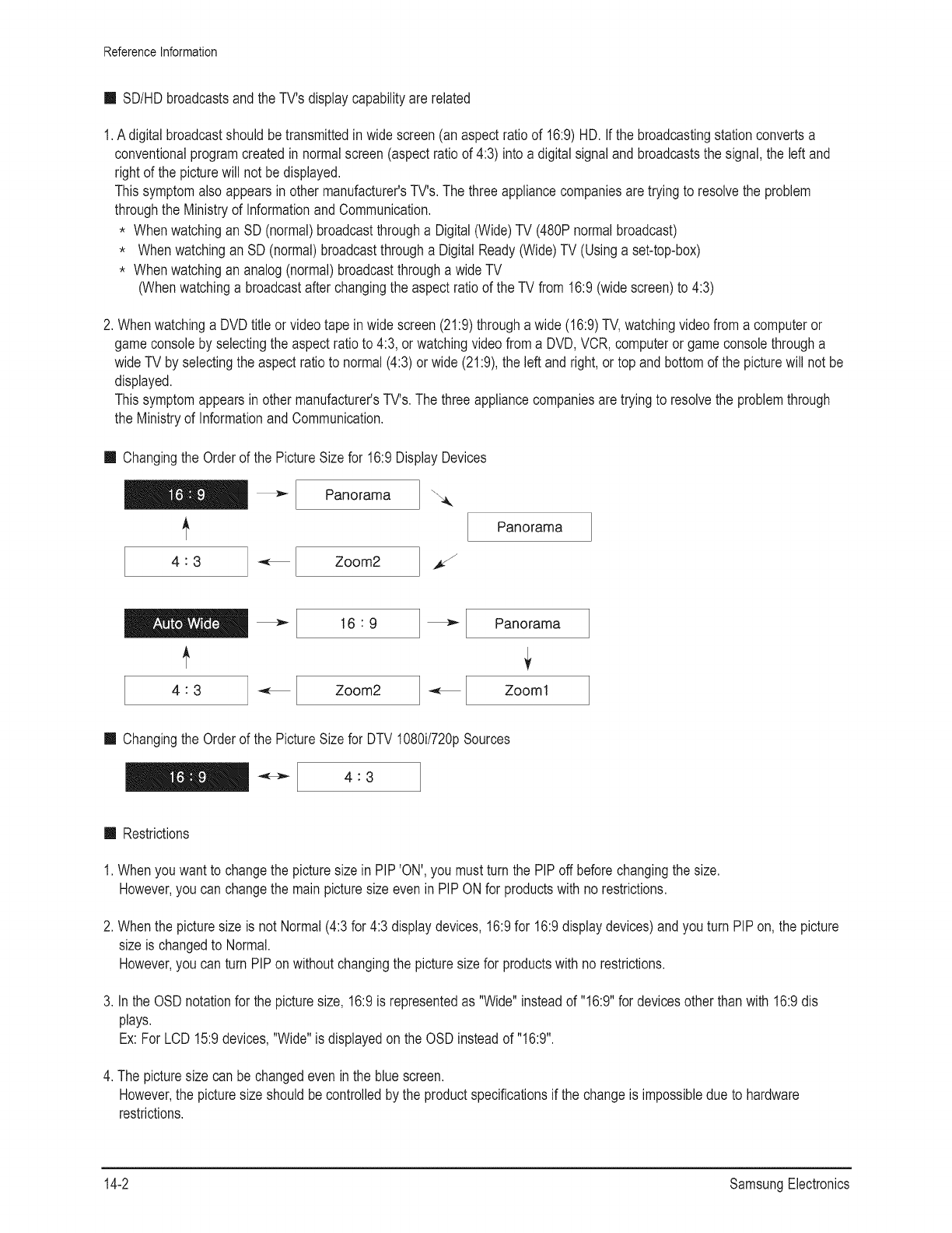
ReferenceInformation
II SD/HDbroadcastsandthe TV's displaycapabilityare related
1.Adigital broadcastshouldbetransmittedin widescreen(anaspectratioof 16:9)HD. Ifthe broadcastingstationconvertsa
conventionalprogramcreatedin normalscreen(aspectratioof 4:3) intoa digitalsignalandbroadcaststhe signal,the leftand
rightof the picturewill not be displayed.
Thissymptomalso appearsin othermanufacturer'sTV's.The threeappliancecompaniesaretryingto resolvethe problem
throughthe Ministryof Informationand Communication.
* Whenwatchingan SD (normal)broadcastthrougha Digital(Wide)TV (480Pnormalbroadcast)
* Whenwatchingan SD (normal)broadcastthrougha DigitalReady(Wide)TV (Usinga set-top-box)
* Whenwatchingan analog(normal)broadcastthrougha wide TV
(Whenwatchinga broadcastafterchangingthe aspectratioof theTV from 16:9(widescreen)to 4:3)
2. Whenwatchinga DVDtitleor videotape inwide screen(21:9)througha wide (16:9)TV,watchingvideofroma computeror
gameconsoleby selectingthe aspectratioto 4:3, orwatchingvideofroma DVD,VCR, computerorgameconsolethrougha
wide TV by selectingthe aspectratio to normal(4:3)or wide(21:9),the left andright,ortop and bottomof the picturewill not be
displayed.
Thissymptomappearsinother manufacturer'sTV's.The threeappliancecompaniesaretryingto resolvethe problemthrough
the Ministryof InformationandCommunication.
II Changingthe Orderof
4:3 1
the PictureSizefor 16:9DisplayDevices
/ Panorama
h
L Zoom2
Panorama
E
_ 16:9 Panorama
Zoom1
II Changingthe Orderof the PictureSizefor DTV1080i/720pSources
II Restrictions
1.Whenyou wantto changethe picturesizein PIP'ON',you mustturn the PIP offbeforechangingthesize.
However,youcan changethe mainpicturesizeevenin PIPONfor productswith norestrictions.
2. Whenthe picturesize is not Normal(4:3for 4:3 displaydevices,16:9for 16:9displaydevices)andyou turn PIPon, the picture
sizeis changedto Normal.
However,youcan turn PIPon withoutchangingthe picturesizefor productswith norestrictions.
3. In the OSDnotationfor the picturesize, 16:9is representedas "Wide"insteadof "16:9"for devicesother thanwith 16:9dis
plays.
Ex:For LCD15:9devices,"Wide"is displayedonthe OSD insteadof "16:9".
4. The picturesizecan bechangedeven in the bluescreen.
However,the picturesizeshouldbecontrolledby the productspecificationsif the changeis impossibledue to hardware
restrictions.
14-2 SamsungElectronics

Reference Information
14-2TechnicalTerms
PiP (Picture In Picture)
Afeatureto enabletwovideo imagesbeingdisplayedon one
screenat the sametime. Forinstance,you can see theTV
channelandthe video imageat the sametime.
Digital Broadcasting
TheATSC(AdvancedTelevisionSystemsCommittee)signals
thatthe stationdigitalizesbeforetransferringthe audio/video
signals.
Mono
Asoundsystemthattransmitsvoicesignalsinonly one
channel.It is hardto experiencea 3D effectbut can be runwith
onespeaker.
LNA (Low NoiseAmplifier)
Thisusessatellitetechnologiesto amplifyweaksignalsfor
improvedqualityeven in poorreceptionareas.
Stereo
Asoundsystemthattransmitsvoicesignalsintwochannels
Thisimplements3Deffectsby transmittingto bothspeakers
(left/right).
Analog Broadcasting
The conventionalsysteminwhichthe stationtransfersthe
audio/videosignalsin NTSCformats.
Antenna Terminal
AterminalwhichtheTV antennais connectedto.A round
coaxialcableis connectedto this terminal,whichis usually
usedto watch airbroadcasts.
English Captions (Subtitle)
Afeatureto provideEnglishcaptionsorcharacterinformation
services,whichthe user can useto studyEnglishusingAFKN
broadcastingor videotapesmarkedwith "CC".
AudioNideo Terminal
The old3- or4-channelTV withnoAVterminalhas a lowquali-
ty issuefor video tape.The problemcan be resolvedusingan
AN terminalthat separatesthe audioand videosignals.The
videoterminalis in yellow;the audioterminalis dividedin two,
whitefor leftand redfor right.
External Source
Thisincludessourcesfromthevideo recorder,DTVset-topbox
and DVDplayer,(anythingbut theTV),
DVl-ICable
Oneof the DVIcablesthatcantransferbothdigitalandanalog
signals.
Satellite Broadcasting
Thisusesa satellitesystemto supporta maximumof 100
channelsincludingair servicesand provideshighquality
picturesanywherein the country,evenin poorreceptionareas.
A set-topbox (unbundled)is requiredto watchsatellite
broadcasting.
Closed Broadcasting
OtherthanVHFand UHF,this includesmovies,entertainment
andeducationalprogramsbroadcastby hotelsorschools.This
is differentfromcablebroadcasting.
Multiplexing
Twolanguagesareprovidedat the sametimewhenbroadcast-
ingforeignmovies,dramasand newsprograms.Youcan
chooseeithera nativeor foreignlanguage,or choosebothat
the sametime.
Component Terminal(Green, Blue, Red)
Thisprovidesmaximumqualityby dividingthe contrastsignals
beforetransferring.
Cable Broadcasting
Comparedto air broadcasting,it usesthe cablesystemto
transferthe signals.Youshouldsubscribeto a local cable
broadcastingcompanyandinstalla separatereceiver.
Tuner
A deviceusedto selecta particularfrequencyfromthe TV set
or the radioreceiver,
Anynet
AnAV networkingsystemof Samsung'svariousAVdevices,
whichenablesthe userto convenientlycontrolAVdevices
usingthe TV.
DVD(DigitalVersatileDisc)
Thisis a CD-sized,highstoragediskthatcan storemultimedia
dataincludingvideos,gamesandaudioapplicationsusing
MPEG-2compressiontechnology.
DVl (Digital Visual Interface)Terminal
Thisis a digitalsignalingstandard.
ThisusesTMDSto reducethe signallossratefor sharper
images.
DVI-DCable
Oneof the DVIcablesthat canonly transferdigitalsignals.
HDMI(High DefinitionMultimedia Interface)
An interfaceintowhichthe digitalsignalsas well as the high
qualityimagedatacan be connectedwithonecable.Thereis
no needto compressthe bit rate.
SamsungElectronics 14-3
ReferenceInformation
S-video Terminal
Thisis, called"Super-video",dividedinto videoandcolorsig-
nalsfor sharperimagedisplay,
VHF/UHF
VHFrefersto the 2 - 13channelsystem;UHFindicatesthe
14- 69 channelsystem,
14-4 SamsungElectronics
ELECTRONICS
ThisServiceManualis a propertyof SamsungElectronicsCo,,Ltd,
Any unauthorizeduseof Manualcan bepunishedunderapplicable
Internationaland/ordomesticlaw.
© Samsung Electronics Co., Ltd. Jul. 2005
Printed in Korea
AA82-02861A
