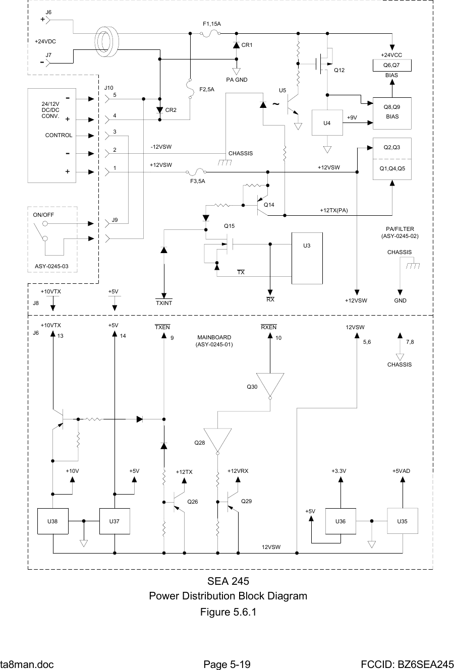
SEA of Delaware SEA245 SEA 245 MF/HF DSC Marine Radiotelephone User Manual MARCH 18 FIRST DRAFT

SEA Inc of Delaware SEA 245 MF/HF DSC Marine Radiotelephone MARCH 18 FIRST DRAFT

sea245 preliminary users manual

FIRST DRAFT 10-7-99V1.01 4-10-00V1.02 10-20-00V1.03 12-1-00V1.04 2-2-01V1.05 5-31-01SEA INC OF DELAWAREPRELIMINARY MAINTENANCE MANUALMF/HF SSB GMDSS RADIOTELEPHONE/DSCCONTROLLERMODEL SEA 245(c) Copyright 2001SEA, Inc.All rights reserved.SEA, Inc.7030 220th St. S.W.Mountlake Terrace, Washington  98043(425)  771-2182FAX: (425)  771-2650
ta8man.doc Page ii FCCID: BZ6SEA245**IMPORTANT**NOTICE TO INSTALLERS-------------------------------------------------------------------NOTE:  The safe compass distance for this equipment (As defined in Paragraph 29 ofIEC Publication 92-101, Third Edition):SEA 245 SINGLE SIDEBAND TRANSCEIVER = 2.0 meters-------------------------------------------------------------------
ta8man.doc Page iii FCCID: BZ6SEA245TABLE OF CONTENTS1 GENERAL INFORMATION .............................................................................................................................. 1-11.1 DESCRIPTION ...................................................................................................................................................1-11.2 EQUIPMENT FURNISHED ..............................................................................................................................1-21.3 TRANSCEIVER UNIT SPECIFICATIONS......................................................................................................1-21.4 MECHANICAL INFORMATION .....................................................................................................................1-21.5 ELECTRICAL SPECIFICATIONS:...................................................................................................................1-22 OPERATION ......................................................................................................................................................... 2-12.1 WARM UP CAUTION .......................................................................................................................................2-12.2 FRONT PANEL CONTROLS............................................................................................................................2-12.3 PROPAGATION .................................................................................................................................................2-12.4 BANDWIDTH LIMITATIONS .........................................................................................................................2-23 MODE AND FREQUENCY CONTROL........................................................................................................... 3-13.1 GENERAL...........................................................................................................................................................3-13.2 SEA 245 FREQUENCY LISTING.....................................................................................................................3-23.3 CAUTION!  FREQUENCY TOLERANCE.................................................................................................... 3-473.4 SETTING THE TRANSMITTER FREQUENCIES....................................................................................... 3-484 INSTALLATION................................................................................................................................................... 4-14.1 MOUNTING THE TRANSCEIVER..................................................................................................................4-14.2 A TYPICAL INSTALLATION ..........................................................................................................................4-14.3 THE TRANSCEIVER UNIT REAR PANEL CONNECTION AND FUSES..................................................4-14.4 FUSING ...............................................................................................................................................................4-44.5 THE GROUND CONNECTION ........................................................................................................................4-55 THEORY OF OPERATION................................................................................................................................5-15.1 GENERAL...........................................................................................................................................................5-15.2 THE RECEIVER .................................................................................................................................................5-15.3 THE TRANSMITTER ........................................................................................................................................5-75.4 THE MASTER CLOCK OSCILLATOR AND SYNTHESIZER SYSTEM ................................................. 5-115.5 THE 2187.5 KHZ MONITOR RECEIVER...................................................................................................... 5-145.6 THE POWER SUPPLY CIRCUIT .................................................................................................................. 5-185.7 THE MAINBOARD CONTROLLER AND DSP PROCESSORS................................................................ 5-216 THE SEA 245 FRONT PANEL/CONTROLLER SYSTEM ........................................................................... 6-16.1 GENERAL...........................................................................................................................................................6-16.2 THEORY OF OPERATION...............................................................................................................................6-1
ta8man.doc Page iv FCCID: BZ6SEA245LIST OF FIGURES2.1   FRONT VIEW OF SEA 245............................................................................................................................... 2-15.2.1  RECEIVER BLOCK DIAGRAM ....................................................................................................................... 5-25.3.1  TRANSMITTER BLOCK DIAGRAM .............................................................................................................. 5-65.4.1  SYNTHESIZER BLOCK DIAGRAM.............................................................................................................. 5-125.5.1  2187.5 KHZ MONITOR BLOCK DIAGRAM................................................................................................ 5-145.6.1  POWER DISTRIBUTION BLOCK DIAGRAM ............................................................................................ 5-175.7.1  MAINBOARD CPU AND DSP BLOCK DIAGRAM .................................................................................... 5-20
ta8man.doc Page 1-1 FCCID: BZ6SEA2451 GENERAL INFORMATION1.1 DESCRIPTIONThe SEA 245 is a compact, all solid-state, 150-Watt PEP, MF/HF SSBRadiotelephone Transceiver/DSC Controller.  The SEA 245 is Type Certified foruse in Sea Area A2 GMDSS stations and it suitable for use in any general purposeMF/HF radiotelephone application.The SEA 245 covers the 1.605 to 29.999 MHz frequency range with channelrestrictions which are determined only by the rules regarding the appropriate radioservice.  As normally programmed, the SEA 245 frequency memory contains ALLnormally assigned ITU VOICE and TELEX channels and has space available forany additional channels which might be desired.The SEA 245 is fully synthesized with 10 Hz resolution and the channel frequenciesare controlled by a precision crystal housed in a temperature-stabilized enclosure. The transceiver is designed to operate from a 24-Volt power system.  Grounding thechassis of the SEA 245 will NOT ground either supply voltage rail.  The SEA 245 isnormally configured as a conventional locally controlled radiotelephone with abacklit 19 key keypad and large backlit LCD graphics display.  The outputimpedance is 50 ohms and the radiotelephone is certified for operation directly intosuitable 50 ohm antenna systems in the 2000 kHz to 27.5 MHz frequency range.When operation in the 1605 to 2000 KHz frequency range is required (FCC pp80.905 and pp 80.909 "Maritime Services; General Exemption for Small PassengerVessels Operated on Domestic Voyages" as amended June 19, 1991), it isMANDATORY that the SEA 245 be operated with either the companion SEA 1635antenna tuner or the standard SEA 1612C or SEA 1631 antenna tuners.The usual MARINE applications will employ an antenna tuner to properly matchthe antenna to the 50 ohm impedance required by the radiotelephone.  For theseapplications, the SEA 245 is designed to operate interactively with either the SEA1635, SEA 1612C or SEA 1631 antenna tuners.  See installation diagrams fordetails on system interconnections.The SEA 245 may also be operated from a single remote location using SEA 2450Remote Controllers and the upgraded SEABUSS(c) interconnection provided.The SEA 245 is also provided with an independent RS232 port which provides foreasy interconnection with a computer.
ta8man.doc Page 1-2 FCCID: BZ6SEA2451.2 EQUIPMENT FURNISHED1.2.1 SEA 245 MF/HF Single Sideband Transceiver1.2.2 Transceiver Mounting Bracket1.2.3 Microphone and Microphone Clip1.2.4 Power Connector1.2.5 SEABUSS Connector, 9 pin PHOENIX type, female1.2.6 Accessory Connector, 14 pin PHOENIX type, female1.2.7 SEA 245 Operator's Manual1.3 TRANSCEIVER UNIT SPECIFICATIONS1.4 MECHANICAL INFORMATION1.4.1 DIMENSIONS:  (HEIGHT-WIDTH-DEPTH)  In:  3.9 x 10.5 x 10.5  mm:  99 x 265 x 2651.4.2 WEIGHT:  Lbs:  10  Kgs:  4.51.5 ELECTRICAL SPECIFICATIONS:Type Acceptance FCC Parts 80, 87, 90FCC IDENTIFIER BZ6SEA245Frequency Range (Tx) 1.605 - 29.999 MHz(Rx) 0.490 - 29.999 MHzCircuitry Double Conversion, 45 MHz 1st IF, 40 kHz(nominal) DSPOperating Controls 19 Key Keypad, Volume ControlChannel Capacity 976 Marine ITU Channels in permanentstorage, 200 scratchpad channels
ta8man.doc Page 1-3 FCCID: BZ6SEA245Operating Temperature -30 degrees to +60 degrees CFrequency Stability + 10 HzOperating Modes J3E, R3E, H3E (2182 kHz), A1A (CW), F2B(TELEX)Primary Voltage 24 V DC –10, +25% (21.6 to 30 V DC)Current Drain:Receive (Standby) 1 AmpReceive (Full Audio) 1.5 AmpsTransmit (Average Voice) 6 AmpsTransmit (Two Tone) 8 AmpsTransmit (TELEX) 12 AmpsRF Impedance 50 Ohms1.5.1 TRANSMITTERPower Output R3E, J3E 150 Watts PEPF2B 100 WattsLOW = 50 - 75 WattsVLOW = 25 - 40 WattsIntermodulation (J3E) -34 dB below PEP (3rd)Spurious Emissions -65 dB below PEPCarrier Suppression -46 dB below PEPUnwanted Sideband (@1000Hz) -41 dB below PEPAudio Response (J3E) 400 - 2500 Hz (@ -6 dB)Hum and Noise -46 dB below PEPTx Attack Time ≥ 15 ms1.5.2 RECEIVERSensitivity, J3E ≥ 2.0 MHz ≤ 1 μV for 12 dB SINADBandwidth, J3E 400 - 2500 Hz (@ -6 dB)Selectivity, J3E at -1 kHz ≤ -55 dBAGC, J3E Fast attack, slow release, ≤ 10 dB audio levelchange  from 10 μV to 100 mV inputIntermodulation ≤ -80 dB
ta8man.doc Page 1-4 FCCID: BZ6SEA245Spurious Responses ≤ -60 dBAudio Output 4 W with ≤ 10% distortion into external 4ohm load.Internal Loudspeaker 2.5" round, 4 ohm, 2 WattSpurious Radiation Complies with FCC, EIA
ta8man.doc Page 1-5 FCCID: BZ6SEA245SEA 245 FRONT VIEW (see separate attachment)FIGURE 2.1  SEA 245 FRONT VIEW
ta8man.doc Page 2-1 FCCID: BZ6SEA2452 OPERATION2.1 WARM UP CAUTIONDo not attempt to transmit until the radiotelephone is warmed up for at least 1minute.  Transmitting before the 1-minute warm-up period has elapsed can causeviolation of FCC regulations.2.2 FRONT PANEL CONTROLSFigure 1 illustrates the front panel of the SEA 245.  The function of the individualcontrols and indicators are listed below.2.2.1 ROTARY CONTROLOne rotary control is provided.  This is the ON/OFF VOLUME control.  Rotatingthe control clockwise from the extreme counter-clockwise position will switch thepower ON.  Further clockwise rotation adjusts the receiver loudspeaker volume tothe desired level.  Note that this control does NOT adjust the SEABUSS audio level.2.2.2 KEYPADAll of the various operating functions of a MF/HF radiotelephone and a Class ADigital Selective Calling Controller are realized through the 19 key keypad on theSEA 245 front panel, together with an interactive system of menus on the frontpanel LCD.  For more specific details regarding the operating system, refer to theSEA 245 Operators Manual (OPR-245).2.2.3 LCD DISPLAYThe LCD display used in the SEA 245 is an LED backlit graphics display module. This technology provides a fully reprogrammable display that facilitates the manydifferent display requirements for a combination Radiotelephone/DSC Controller.2.3 PROPAGATIONMF/HF radio signals propagate far beyond the horizon.  MF frequencies (2-3 MHz)are generally usable within 300 miles depending on the time of day, atmosphericconditions and man-made noise levels.The High Seas frequencies (4, 6, 8, 12, 18, 22 and 25 MHz) allow communicationsover thousands of miles, again subject to the above mentioned limitations,Interference tends to be more of a problem on the MF/HF bands than on VHFchannels.To promote a more in-depth understanding of the vicissitudes of MF/HFcommunications, SEA's "Mariners Guide to Single Sideband" (MAN-0001-001) is
ta8man.doc Page 2-2 FCCID: BZ6SEA245highly recommended reading.2.4 BANDWIDTH LIMITATIONSThe only limitation imposed by the SEA 245 is that the desired frequency be insidethe operating range of the equipment.  In practice the antenna system will have agreat deal to do with dictating the maximum allowable frequency separation.  If (asis usually the case) a companion antenna tuner such as the SEA 1635 or SEA 1612Cin used in conjunction with the usual short whip antenna, the allowable 2 MHz splitmay be reduced to a few hundred kHz.
ta8man.doc Page 3-1 FCCID: BZ6SEA2453  MODE AND FREQUENCY CONTROL3.1 GENERALIn the SEA 245, the frequency of operation is determined through a combination ofcoarse and fine tuning mechanisms.  The coarse tuning system consists of the PLLcircuitry associated with the first Local Oscillator VCO.  The effective loopfrequency of the PLL is 4 kHz and the first LO is preset to the nearest incrementalfrequency needed to convert the desired operating frequency to 45 MHz.  Therequired divide-by-N number for a given operating frequency is calculated by thecontrol microprocessor and then loaded into the main loop PLL chip through themicroprocessor SPI bus.  The fine tuning system is incorporated into the DSPalgorithm, which operates as the receiver “back end” and the transmitter "front end". The PLL that controls the second conversion oscillator is also loaded through themicroprocessor SPI bus.Such data as filter band, VCO band, synthesizer loads, carrier status and DSPalgorithm are calculated and stored in appropriate registers by the controllercomputer, once the desired channel is entered by the operator.3.1.1 TRANSMITTER MODE SELECTIONThe primary mode of operation of the SEA 245 is in the J3E (SSB with fullysuppressed carrier) mode.Two auxiliary VOICE modes are also provided:R3E:  SSB with pilot carrier re-inserted 16 dB below PEP.H3E:  SSB with pilot carrier re-inserted 6 dB below PEP.J3E is the basic SSB operating mode and is used for virtually all VOICEcommunications.  H3E (AME) is used to provide a degree of compatibility betweenold style AM and SSB systems.  Present practice limits this mode to 2182.0 kHzONLY.  R3E is primarily used to provide a pilot carrier on public correspondencechannels.  Present practice ignores this mode.J2B:  TELEX operation with both internally and externally generated (AFSK) tones. Uses J3E mode with narrower bandpass filter.  Note that the internal DSC systemuses the same standard 1700 Hz subcarrier frequency as is used in the SEA 3000SEATOR equipment.3.1.2 RECEIVE MODE SELECTIONThe SEA 245 supports J3E, R3E and H3E modes as a standard SSB (J3E) receiver. The passband filter and AGC characteristics are tailored for SSB VOICE operation.In the TELEX (J2B) receive mode, the passband filter is shifted to narrowband (500
ta8man.doc Page 3-2 FCCID: BZ6SEA245Hz) and the BFO offset is set to the International Standard of 1700 Hz.  AGC is fastattack, fast release.In the CW (A1A) receive mode, the receiver passband filter is shifted to narrowband(500 Hz) and the BFO offset is set to 1000 Hz.  AGC is fast attack, fast release.In the AM (A3E) receive mode, the receiver passband is shifted to maximumbandwidth (4 kHz) and the received signal carrier is offset 1 kHz from the passbandcenter.  The DSP based envelope detector provides "true" AM demodulation with aneffective bandwidth of 3000 Hz for audio recovery.  This mode is useful primarilyin the reception of time signals from WWV, shortwave broadcast signal etc.  AGCis fast attack, fast release.3.2 SEA 245 FREQUENCY LISTING3.2.1 2 MHZ VOICE BANDVOICECHANNELSHIPRECEIVESHIPTRANSMIT USE201 2003.0 2003.0 Ship-to-Ship, Great Lakes202 2450.0 2003.0 KMI Point Reyes, CA203 2006.0 2006.0 Alaska205 2446.0 2009.0 WLO, Mobile, AL206 2506.0 2009.0 WAH, St. Thomas208 2030.0 2030.0 Virgin Islands, Intership209 2490.0 2031.5 WOM, Ft. Lauderdale, FL211 2054.0 2054.0 British Columbia WX212 2065.0 2065.0 Ship-to-Ship213 2079.0 2079.0 Ship-to-Ship214 2082.5 2082.5 Ship-to-Ship Only215 2086.0 2086.0 Ship-to-Ship, Miss. RiverLimited Coast216 2585.0 2086.0 KRV, Pence Playa,WAH, St. Thomas, VI217 2093.0 2093.0 Ship-to-Ship OnlyCommercial Fish218 2096.5 2096.5 Ship-to-Ship,
ta8man.doc Page 3-3 FCCID: BZ6SEA245Ship to Limited Coast Station219 2115.0 2115.0 Alaska220 2118.0 2118.0 Alaska221 2514.0 2118.0 WOM, Ft. Lauderdale, FLWLC, Rogers City, MI223 2309.0 2131.0 WOU-23, Kodiak, AK224 2312.0 2134.0 WGG-53, Cold Bay, AK225 2530.0 2134.0 KBP, Kahuka, HI,KOP, Galveston226 2134.0 2134.0 Eastern Canada Intership227 2538.0 2142.0 KCC, Corpus Christi, TX228 2142.0 2142.0 CA Intership229 2146.0 2146.0230 2550.0 2158.0 PJC, Curacao231 2550.0 2166.0 VRT, Bermuda232 2558.0 2186.0 WOO, Manahawkin, NJ233 2582.0 2166.0 8PO, Barbados,C6XZ, Marsh Harbor234 2558.0 2198.0 VPN-2, Nassau Weather236 2203.0 2203.0 Ship-to-Ship, Gulf of Mexico238 2582.0 2206.0 WBL, Buffalo, NYVCS, Halifax, Canada239 2397.0 2237.0 WDV-26, CordovaWGG-56, Ketchikan, AK240 2400.0 2240.0 WGG-58, Juneau, AKWGG-55, Nome, AK241 2735.0 2290.0 9YL, North Post, Trinidad242 2450.0 2366.0245 2566.0 2390.0 WOM, Ft Lauderdale, FL246 2400.0 2400.0247 2442.0 2406.0 WOM, Ft Lauderdale, FL
ta8man.doc Page 3-4 FCCID: BZ6SEA245248 2506.0 2406.0 KMI, Point Reyes, CA249 2419.0 2419.0 Alaska250 2422.0 2422.0 Alaska251 2427.0 2427,0 Alaska252 2572.0 2430.0 WLO, Mobile, AL254 2430.0 2430.0 Alaska255 2447.0 2447.0 Alaska256 2450.0 2450.0 Alaska257 2506.0 2458.0 KGN, Delcambre, LA258 2479.0 2479.0 Alaska259 2482.0 2482.0 Alaska261 2506.0 2506.0 Alaska262 2509.0 2509.0 Alaska263 2512.0 2512.0 FFP, Ft. Defrance,Windward Is.264 2545.0 2545.0265 2527.0 2527.0 Alaska266 2535.0 2535.0267 2538.0 2538.0 Alaska268 2563.0 2583.0 Alaska269 2566.0 2566.0 Alaska270 2582.0 2582.0 Alaska271 2590.0 2590.0 Alaska273 2616.0 2616.0 Alaska275 2638.0 2638.0 Ship-to-Ship276 2640.0 2640.0277 2670.0 2870.0 USCG Working278 2704.0 2704.0 Ocean Racing279 2735.0 2735.0 9YL, North Post, Trinidad280 2738.0 2738.0 Ship-to-ShipExcept Great Lakes and Gulf
ta8man.doc Page 3-5 FCCID: BZ6SEA245281 2782.0 2782.0 Ship-to-Ship RiverWFN, Jeffersonville, INWGK, St. Louis, MOWJG, Memphis, TN282 2830.0 2830.0 Ship-to-Ship, Gulf Only283 2237.0 2237.0284 2530.0 2815.0285 2040.0 2040.0286 2318.0 2318.0287 2366.0 2366.0288 2469.0 2708.0289 2060.0 2798.0290 2458.0 2340.0291 2085.0 2045.0 NORWEGIAN292 2048.0 2048.0 NORWEGIAN293 2051.0 2051.0 NORWEGIAN294 2057.0 2057.0 NORWEGIAN302 3198.0 3198.0 Alaska Point-to-Point303 3201.0 3201.0 Alaska Point-to-Point304 3258.0 3258.0 Alaska305 3261.0 3261.0 Alaska306 3449.0 3449.0 Alaska Aero3.2.2 4 MHZ VOICE BANDVOICECHANNELSHIPRECEIVESHIPTRANSMIT USE401 4357.0 4065.0 KMI, Point Reyes, CAWAH, St. Thomas, VI402 4360.0 4068.0
ta8man.doc Page 3-6 FCCID: BZ6SEA245403 4363.0 4071.0 WOM, Ft. Lauderdale, FL404 4366.0 4074.0 KGN, Delcambre, LA405 4369.0 4077.0 WLO, Mobile, ALWLC, Roger City, MI406 4372.0 4080.0407 4375.0 4083.0408 4378.0 4086.0409 4381.0 4089.0410 4384.0 4092.0 WOO, Manahawkin, NJ411 4387.0 4095.0 WOO, Manahawkin, NJ412 4390.0 4098.0 WOM, Ft. Lauderdale, FL413 4393.0 4101.0414 4396.0 4104.0 WLO, Mobile, AL415 4399.0 4107.0416 4402.0 4110.0 KMI, Point Reyes, CAWOO, Manahawkin, NJ417 4405.0 4113.0 KMI, Point Reyes, CAWOM, Ft. Lauderdale, FL418 4408.0 4116.0419 4411.0 4119.0 WLO, Mobile, AL420 4414.0 4122.0421 4417.0 4125.0422 4420.0 4128.0 WOO, Manahawkin, NJ423 4423.0 4131.0 WOM, Ft. Lauderdale, FL424 4426.0 4134.0 NMG, New Orleans, LANMN, Portsmouth, VA, WX425 4429.0 4137.0426 4432.0 4140.0427 4435.0 4143.0428 4351.0 4060.0 WLO, Mobile, AL
ta8man.doc Page 3-7 FCCID: BZ6SEA245450 4125.0 4125.0 DISTRESS451 4146.0 4146.0 4A LTD Coast/Intership452 4149.0 4149.0 4B LTD Coast/Intership453 4417.0 4417.0 4C LTD Coast/Intership454 4366.0 4366.0 Alaska455 4369.0 4369.0 Alaska456 4396.0 4396.0 Alaska457 4402.0 4402.0 Alaska458 4420.0 4420.0 Alaska459 4423.0 4423.0 Alaska460 4065.0 4065.0 Mississippi River461 4089.0 4089.0 Mississippi River462 4116.0 4116.0 Mississippi River463 4408.0 4408.0 Mississippi River501 5164.5 5164.5 Alaska Public Fixed502 5167.5 5167.5 Alaska Emergency/Calling503 5680.0 5680.0 Aero Search/Rescue504 5472.0 5472.0 Aero Search/Rescue505 5490.0 5490.0 Aero3.2.3 6 MHZ VOICE BANDVOICECHANNELSHIPRECEIVESHIPTRANSMIT USE601 6501.0 6200.0 NMN, Portsmouth, VANMG, New Orleans, LAMNA, Miami, FL602 6504.0 6203.0603 6507.0 6206.0604 6510.0 6209.0
ta8man.doc Page 3-8 FCCID: BZ6SEA245605 6513.0 6212.0606 6516.0 6215.0607 6519.0 6218.0 WLO, Mobile, AL608 6522.0 6221.0650 6215.0 6215.0 DISTRESS651 6224.0 6224.0 6A LTD Coast/Intership652 6227.0 6227.0 6B LTD Coast/Intership653 6230.0 6230.0 6C LTD Coast/Intership654 6516.0 6616.0 6D LTD CoastDAYTIME ONLY655 6209.0 6209.0 Mississippi River656 6212.0 6212.0 Mississippi River657 6510.0 6510.0 Mississippi River658 6513.0 6513.0 Mississippi River3.2.4 8 MHZ VOICE BANDVOICECHANNELSHIPRECEIVESHIPTRANSMIT USE801 8719.0 8195.0802 8722.0 8198.0 WOM, Ft. Lauderdale, FL803 8725.0 8201.0804 8728.0 8204.0 KMI, Point Reyes, CA805 8731.0 8207.0 WOM, Ft. Lauderdale, FL806 8734.0 8210.0807 8737.0 8213.0808 8740.0 8216.0 WOO, Manahawkin, NJ809 8743.0 8219.0 KMI, Point Reyes, CA810 8746.0 8222.0 WOM, Ft. Lauderdale, FL811 8749.0 8225.0 WOO, Manahawkin, NJ
ta8man.doc Page 3-9 FCCID: BZ6SEA245812 8752.0 8228.0813 8755.0 8231.0814 8758.0 8234.0 WOM, Ft. Lauderdale, FL815 8761.0 8237.0 WOO, Manahawkin, NJ816 8764.0 8240.0817 8767.0 8243.0818 8770.0 8246.0819 8773.0 8249.0820 8776.0 8252.0821 8779.0 8255.0822 8782.0 8258.0 KMI, Point Reyes, CA823 8785.0 8261.0824 8788.0 8264.0 WLO, Mobile, AL825 8791.0 8267.0 WOM, Ft. Lauderdale, FL826 8794.0 8270.0 WOO, Manahawkin, NJWLC, Rogers City, MI827 8797.0 8273.0828 8800.0 8276.0829 8803.0 8279.0830 8806.0 8282.0 WLO, Mobile, AL831 8809.0 8285.0 WOM, Ft. Lauderdale, FL832 8812.0 8288.0833 8291.0 8291.0836 8713.0 8113.0 WLO, Mobile, AL837 8716.0 8128.0 KGN, Delcambre, LA850 8291.0 8291.0 DISTRESS851 8294.0 8294.0 8A LTD Coast/Intership852 8297.0 8297.0 8B LTD Coast/Intership853 8201.0 8201.0 WFN, Jeffersonville,Mississippi. River
ta8man.doc Page 3-10 FCCID: BZ6SEA245854 8213.0 8213.0 WGK, St. Louis, Miss. River855 8725.0 8725.0 Mississippi River856 8737.0 8737.0 Mississippi River3.2.5 12 MHZ VOICE BANDVOICECHANNELSHIPRECEIVESHIPTRANSMIT USE1201 13077.0 12230.0 KMI, Point Reyes, CA1202 13080.0 12233.0 KMI, Point Reyes, CA1203 13083.0 12236.0 KMI, Point Reyes, CA1204 13086.0 12239.01205 13089.0 12242.01206 13092.0 12245.0 WOM, Ft. Lauderdale, FL1207 13095.0 12248.01208 13098.0 12251.0 WOM, Ft. Lauderdale, FL1209 13101.0 12254.0 WOM, Ft. Lauderdale, FL1210 13104.0 12257.0 WOO, Manahawkin, NJ1211 13107.0 12260.0 WOO, Manahawkin, NJ1212 13110.0 12263.0 WLO, Mobile, AL1213 13113.0 12266.01214 13116.0 12269.0 USCG, Miami/Portsmouth1215 13119.0 12272.0 WOM, Ft. Lauderdale, FL1216 13122.0 12275.01217 13125.0 12278.01218 13128.0 12281.01219 13131.0 12284.01220 13134.0 12287.01221 13137.0 12290.01222 13140.0 12293.01223 13143.0 12296.0 WOM, Ft. Lauderdale, FL
ta8man.doc Page 3-11 FCCID: BZ6SEA2451224 13146.0 12299.01225 13149.0 12302.01226 13152.0 12305.01227 13155.0 12308.01228 13158.0 12311.0 WOO, Manahawkin, NJ1229 13161.0 12314.0 KMI, Point Reyes, CA1230 13164.0 12317.0 WOM, Ft. Lauderdale, FL1231 13167.0 12320.01232 13170.0 12323.01233 13173.0 12326.0 WLO, Mobile, AL1234 13176.0 12329.01235 13179.0 12332.0 WLO, Mobile, AL1236 13182.0 12335.01234 13176.0 12329.01235 13179.0 12332.0 WLO, Mobile, AL1236 13182.0 12335.0 KGN, Delcambre, LA1237 13185.0 12338.01238 13188.0 12341.01239 13191.0 12344.01240 13194.0 12347.01241 13197.0 12350.01250 12290.0 12290.0 DISTRESS1251 12353.0 12353.0 12A LTD Coast/Intership1252 12356.0 12356.0 12B LTD Coast/Intership1253 12359.0 12359.0 12C LTD Coast/Intership1254 12362.0 12362.0 PUB. COAST & Miss. River1255 12365.0 12365.0 PUB. COAST & Miss. River
ta8man.doc Page 3-12 FCCID: BZ6SEA2453.2.6 16 MHZ VOICE BANDVOICECHANNELSHIPRECEIVESHIPTRANSMIT USE1601 17242.0 16360.0 WOM, Ft. Lauderdale, FL1602 17245.0 16363.0 KMI, Point Reyes, CA1603 17248.0 16366.0 KMI, Point Reyes, CA1604 17251.0 16369.01605 17254.0 16372.0 WOO, Manahawkin, NJ1606 17257.0 16375.01607 17260.0 16378.01608 17263.0 16381.01609 17266.0 16384.0 WOM, Ft. Lauderdale, FL1610 17269.0 16387.0 WOM, Ft. Lauderdale, FL1611 17272.0 16390.0 WOM, Ft. Lauderdale, FL1612 17275.0 16393.01613 17278.0 16396.01614 17281.0 16399.01615 17284.0 16402.01616 17287.0 16405.0 WOM, Ft. Lauderdale, FL1617 17290.0 16408.01618 17293.0 16411.01619 17296.0 16414.01620 17299.0 16417.0 WOO, Manahawkin, NJ1621 17302.0 16420.01622 17305.0 16423.01623 17308.0 16426.01624 17311.0 16429.0 KMI, Point Reyes, CA1625 17314.0 16432.0 USCG, Miami, Portsmouth1626 17317.0 16435.0 WOO, Manahawkin, NJ1627 17320.0 16438.01628 17323.0 16441.0
ta8man.doc Page 3-13 FCCID: BZ6SEA2451629 17326.0 16444.01630 17329.0 16447.01631 17332.0 16450.0 WOO, Manahawkin NJ1632 17335.0 16453.01633 17338.0 16456.01634 17341.0 16459.01635 17344.0 16462.01636 17347.0 16465.01637 17350.0 16468.01638 17353.0 16471.01639 17356.0 16474.01640 17359.0 16477.01641 17362.0 16480.0 WLO, Mobile, AL1642 17365.0 16483.01643 17368.0 16486.0 WLO, Mobile, AL1644 17371.0 16489.01645 17374.0 16492.0 KGN, Delcambre, LA1646 17377.0 16495.01647 17380.0 16498.0 WLO, Mobile, AL1648 17383.0 16501.01649 17386.0 16504.01650 16420.0 16420.0 DISTRESS1651 16528.0 16528.0 16A LTD Coast/Intership1652 16531.0 16531.0 16B LTD Coast/Intership1653 16534.0 16534.0 16C LTD Coast/Intership1654 16537.0 16537.01655 16540.0 16540.01656 16543.0 16543.0 PUB. COAST & Miss. River1657 16546.0 16546.0 PUB. COAST & Miss. River
ta8man.doc Page 3-14 FCCID: BZ6SEA2453.2.7 18 MHZ VOICE BANDVOICECHANNELSHIPRECEIVESHIPTRANSMIT USE1801 19755.0 18780.01802 19758.0 18783.01803 19761.0 18786.01804 19764.0 18789.01805 19767.0 18792.01806 19770.0 18795.01807 19773.0 18798.0 WLO, Mobile, AL1808 19776.0 18801.01809 19779.0 18804.01810 19782.0 18807.01811 19785.0 18810.01812 19788.0 18813.01813 19791.0 18816.01814 19794.0 18819.01815 19797.0 18822.01851 18840.0 18840.0 18A LTD Coast/Intership1852 18843.0 18843.0 18B LTD Coast/Intership1853 18825.0 18825.01854 18828.0 18828.01855 18831.0 18831.01856 18834.0 18834.01857 18837.0 18837.03.2.8 22 MHZ VOICE BANDVOICECHANNELSHIPRECEIVESHIPTRANSMIT USE
ta8man.doc Page 3-15 FCCID: BZ6SEA2452201 22896.0 22000.0 WOO, Manahawkin, NJ2202 22699.0 22003.02203 22702.0 22006.02204 22705.0 22009.02205 22708.0 22012.0 WOO, Manahawkin, NJ2206 22711.0 22015.02207 22714.0 22018.02208 22717.0 22021.02209 22720.0 22024.02210 22723.0 22027.0 WOO, Manahawkin, NJ2211 22726.0 22030.02212 22729.0 22033.02213 22732.0 22036.02214 22735.0 22039.0 KMI, Point Reyes, CA2215 22738.0 22042.0 WOM, Ft. Lauderdale, FL2216 22741.0 22045.0 WOM, Ft. Lauderdale, FL2217 22744.0 22048.02218 22747.0 22051.02219 22750.0 22054.02220 22753.0 22057.02221 22756.0 22060.02222 22759.0 22063.0 WOM, Ft. Lauderdale, FL2223 22762.0 22066.0 KMI, Point Reyes, CA2224 22765.0 22069.02225 22768.0 22072.02226 22771.0 22075.02227 22774.0 22078.02228 22777.0 22081.0 KMI, Point Reyes, CA2229 22780.0 22084.02230 22783.0 22087.02231 22786.0 22090.0
ta8man.doc Page 3-16 FCCID: BZ6SEA2452232 22789.0 22093.02233 22792.0 22096.02234 22795.0 22099.02235 22798.0 22102.02236 22801.0 22105.0 KMI, Point Reyes, CAWOO, Manahawkin, NJ2237 22804.0 22108.0 WLO, Mobile, AL2238 22807.0 22111.02239 22810.0 22114.02240 22813.0 22117.02241 22816.0 22120.02242 22819.0 22123.0 WLO, Mobile, AL2243 22822.0 22126.02244 22825.0 22129.02245 22828.0 22132.02246 22831.0 22135.0 WLO, Mobile, AL2247 22834.0 22138.02248 22837.0 22141.02249 22840.0 22144.02250 22843.0 22147.02251 22159.0 22159.0 22A LTD Coast/Intership2252 22162.0 22162.0 22B LTD Coast/Intership2253 22165.0 22165.0 22C LTD Coast/Intership2254 22168.0 22168.0 22D LTD Coast/Intership2255 22171.0 22171.0 22E LTD Coast/Intership2256 22174.0 22174.0 Public Coast2257 22177.0 22177.0 Public Coast
ta8man.doc Page 3-17 FCCID: BZ6SEA2453.2.9 25 MHZ VOICE BANDVOICECHANNELSHIPRECEIVESHIPTRANSMIT USE2501 26145.0 25070.02502 26148.0 25073.02503 26151.0 25076.0 WLO, Mobile, AL2504 26154.0 25079.02505 26157.0 25082.02506 26160.0 25085.02507 26163.0 25088.02508 26166.0 25091.02509 26169.0 25094.02510 26172.0 25097.02551 25115.0 25115.0 25A LTD Coast/Intership2552 25118.0 25118.0 25B LTD Coast/Intership2553 25100.0 25100.02554 25103.0 25103.02555 25106.0 25106.02556 25109.0 25109.02557 25112.0 25112.03.2.10 DSC FREQUENCIESDSCCHANNELSHIPRECEIVESHIPTRANSMITUSE  2174.5   2174.5 NBDP EMER CALLING201   2187.5   2187.5 DSC EMER CALLING202   2177.0   2189.5 INTL DSC CALLING203   2177.0   2177.0 INTERSHIP DSC CALLING401   4207.5   4207.5 DSC EMER CALLING402   4219.5   4208.0 INTL DSC CALLING
ta8man.doc Page 3-18 FCCID: BZ6SEA245403   4220.0   4208.5 ATLANTIC DSC CALLING404   4220.5   4209.0 PACIFIC DSC CALLING601   6312.0   6312.0 DSC EMER CALLING602   6331.0   6312.5 INTL DSC CALLING603   6331.5   6313.0 ATLANTIC DSC CALLING604   6332.0   6313.5 PACIFIC DSC CALLING801   8414.5   8414.5 DSC EMER CALLING802   8436.5   8415.0 INTL DSC CALLING803   8437.0   8415.5 ATLANTIC DSC CALLING804   8437.5   8416.0 PACIFIC DSC CALLING1201 12577.0 12577.0 DSC EMER CALLING1202 12657.0 12577.5 INTL DSC CALLING1203 12657.5 12578.0 ATLANTIC DSC CALLING1204 12658.0 12578.5 PACIFIC DSC CALLING1601 16804.5 16804.5 DSC EMER CALLING1602 16903.0 16805.0 INTL DSC CALLING1603 16903.5 16805.5 ATLANTIC DSC CALLING1604 16904.0 16806.0 PACIFIC DSC CALLING1802 19703.5 18898.5 INTL DSC CALLING1803 19704.0 18899.0 ATLANTIC DSC CALLING1804 19704.5 18899.5 PACIFIC DSC CALLING2202 22444.0 22374.5 INTL DSC CALLING2203 22444.5 22375.0 ATLANTIC DSC CALLING2204 22445.0 22375.5 PACIFIC DSC CALLING2502 26121.0 25208.5 INTL DSC CALLING2503 26121.5 25209.0 ATLANTIC DSC CALLING2504 26122.0 25209.5 PACIFIC DSC CALLING
ta8man.doc Page 3-19 FCCID: BZ6SEA2453.2.11 4 MHZ TELEX BANDTELEXCHANNELSHIPRECEIVESHIPTRANSMITUSE401 4210.5 4172.5 WNU402 4211.0 4173.0 ZLA403 4211.5 4173.5 KFS404 4212.0 4174.0405 4212.5 4174.5 WLO406 4213.0 4175.0 WLO, VIP407 4213.5 4175.5 KBS408 4214.0 4176.0 KLB, WPD409 4214.5 4176.6 KLC410 4215.0 4177.0 WLO411 4177.5 4177.5 NBDP EMER CALLING412 4215.5 4178.0 KBS413 4216.0 4178.5 KPH414 4216.5 4179.0 WCC415 4217.0 4179.5 WLO416 4217.5 4180.0 VCT417 4218.0 4180.5 WLO418 4218.5 4181.0419 4219.0 4181.5471 4202.5 4202.5472 4203.0 4203.0473 4203.5 4203.5474 4204.0 4204.0475 4204.5 4204.5476 4205.0 4205.0477 4205.5 4205.5478 4206.0 4206.0479 4206.5 4206.5
ta8man.doc Page 3-20 FCCID: BZ6SEA245480 4207.0 4207.03.2.12 6 MHZ TELEX BANDTELEXCHANNELSHIPRECEIVESHIPTRANSMITUSE601 6314.5 6263.0 KFS602 6315.0 6263.5 WNU603 6315.5 6264.0 KFS604 6316.0 6264.5605 6316.5 6265.0606 6317.0 62655 WLO607 6317.5 6266.0608 6318.0 6266.5 KLB609 6318.5 6267.0 KLC610 6319.0 6267.5 WLO611 6268.0 6268.0 NBDP EMER CALLING612 6319.5 6268.5613 6320.0 6269.0 KPH614 6320.5 6269.5615 6521.0 6270.0 WLO616 6321.5 6270.5617 6322.0 6271.0 KLC618 6322.5 6271.5619 6323.0 6272.0 WLO620 6323.5 6272.5621 6324.0 6273.0 WCC622 6324.5 62736 KPH, KLC623 6325.0 6274.0624 6325.5 6274.5625 6326.0 6275.0626 6326.5 6275.5
ta8man.doc Page 3-21 FCCID: BZ6SEA245627 6327.0 6281.0628 6327.5 6281.5629 6328.0 6282.0630 6328.5 6282.5631 6329.0 6283.0632 6329.5 6283.5633 6330.0 6284.0634 6330.5 6284.5671 6300.5 6300.5672 6301.0 6301.0673 6301.5 6301.5674 6302.0 6302.0675 6302.5 6302.5676 6303.0 6303.0677 6303.5 6303.5678 6304.0 6304.0679 6304.5 6304.5680 6305.0 6305.0681 6305.5 6305.5682 6306.0 6306.0683 6306.5 6306.5684 6307.0 6307.0685 6307.5 6307.5686 6308.0 6308.0687 6308.5 6308.5688 6309.0 6309.0689 6309.5 6309.5690 6310.0 6310.0691 6310.5 6310.5692 6311.0 6311.0693 6311.5 6311.5
ta8man.doc Page 3-22 FCCID: BZ6SEA2453.2.13 8 MHZ TELEX BANDTELEXCHANNELSHIPRECEIVESHIPTRANSMITUSE801 8376.5 8376.5 NBDP EMER CALLING802 8417.0 8377.0 WNU803 8417.5 8377.5 KFS804 8418.0 8378.0805 8418.5 8378.5 WLO806 8419.0 8379.0 WLO807 8419.5 8379.5808 8420.0 8380.0809 8420.5 8380.5 KLC810 8421.0 8381.0 WLO811 8421.5 8381.5 WLO812 8422.0 8382.0813 8422.5 8382.5 KPH814 8423.0 8383.0815 8423.5 8383.5 WLO816 8424.0 8384.0 WCC817 8424.5 8384.5 KLC818 8425.0 8385.0 KLB819 8425.5 8385.5820 8426.0 8386.0821 8426.5 8386.5 WCC822 8427.0 8387.0 KLC823 8427.5 8387.5824 8428.0 8388.0825 8428.5 8388.5826 8429.0 8389.0 WLO827 8429.5 8389.5
ta8man.doc Page 3-23 FCCID: BZ6SEA245828 8430.0 8390.0829 8430.5 8390.5830 8431.0 8391.0831 8431.5 8391.5832 8432.0 8392.0833 8432.5 8392.5834 8433.0 8393.0835 8433.5 8393.5836 8434.0 8394.0837 8434.5 8394.5838 8435.0 8395.0839 8435.5 8395.5840 8436.0 8396.0871 8396.5 8396.5872 8397.0 8397.0873 8397.5 8397.5874 8398.0 8398.0875 8398.5 8398.5876 8399.0 8399.0877 8399.5 8399.5878 8400.0 8400.0879 8400.5 8400.5880 8401.0 8401.0881 8401.5 8401.5882 8402.0 8402.0883 8402.5 8402.5884 8403.0 8403.0885 8403.5 8403.5886 8404.0 8404.0887 8404.5 8404.5888 8405.0 8405.0
ta8man.doc Page 3-24 FCCID: BZ6SEA245889 8405.5 8405.5890 8406.0 8406.0891 8406.5 8406.5892 8407.0 8407.0893 8407.5 8407.5894 8408.0 8408.0895 8408.5 8408.5896 8409.0 8409.0897 8409.5 8409.5898 8410.0 8410.0899 8410.5 8410.5900 8411.0 8411.0901 8411.5 8411.5902 8412.0 8412.0903 8412.5 8412.5904 8413.0 8413.0905 8413.5 8413.5906 8414.0 8414.03.2.14 12 MHZ TELEX BANDTELEXCHANNELSHIPRECEIVESHIPTRANSMITUSE1201 12579.5 12477.01202 12580.0 12477.5 ZLA1203 12580.5 12478.0 KFS1204 12581.0 12478.51205 12581.5 12479.0 WLO1206 12582.0 12479.5 VIP1207 12582.5 12480.01208 12583.0 12480.51209 12583.5 12481.0 KLC
ta8man.doc Page 3-25 FCCID: BZ6SEA2451210 12584.0 12481.5 VIP1211 12584.5 12482.0 WLO1212 12585.0 12482.51213 12585.5 12483.0 KPH1214 12586.0 12483.51215 12586.5 12484.0 WLO1216 12587.0 12484.51217 12587.5 12485.0 KLC1218 12588.0 12485.51219 12588.5 12486.0 WNU1220 12589.0 12486.51221 12589.5 12487.0 WCC1222 12590.0 12487.5 KLC1223 12590.5 12488.0 KLB1224 12591.0 12488.51225 12591.5 12489.0 WLO1226 12592.0 12489.51227 12592.5 12490.01228 12593.0 12490.51229 12593.5 12491.0 WLO1230 12594.0 12491.51231 12594.5 12492.01232 12595.0 12492.51233 12595.5 12493.01234 12596.0 12493.5 WLO1235 12596.5 12494.01236 12597.0 12494.51237 12597.5 12495.01238 12598.0 12495.5 WCC1239 12598.5 12496.01240 12599.0 12496.5 WLO
ta8man.doc Page 3-26 FCCID: BZ6SEA2451241 12599.5 12497.01242 12600.0 12497.5 KPH1243 12600.5 12498.01244 12601.0 12498.51245 12601.5 12499.01246 12602.0 12499.51247 12602.5 12500.01248 12603.0 12500.5 KLC1249 12603.5 12501.01250 12604.0 12501.5 WLO1251 12604.5 12502.0 WLO1252 12605.0 12502.51253 12605.5 12503.01254 12606.0 12503.5 WLO1255 12606.5 12504.01256 12807.0 12504.51257 12607.5 12505.0 WNU1258 12608.0 12505.51259 12608.5 12506.01260 12609.0 12506.51261 12609.5 12507.01262 12610.0 12507.51263 12610.5 12508.0 VCT1264 12611.0 12508.51265 12611.5 12509.0 KEJ1266 12612.0 12509.51267 12612.5 12510.01268 12613.0 12510.51269 12613.5 12511.01270 12614.0 12511.51271 12614.5 12512.0
ta8man.doc Page 3-27 FCCID: BZ6SEA2451272 12615.0 12512.51273 12615.5 12513.01274 12616.0 12513.51275 12616.5 12514.01276 12617.0 12514.51277 12617.5 12515.01278 12618.0 12515.51279 12618.5 12516.01280 12619.0 12516.51281 12619.5 12517.01282 12620.0 12517.51283 12620.5 12518.01284 12621.0 12518.51285 12621.5 12519.01286 12622.0 12519.51287 12520.0 12520.0 NBDP EMER CALLING1288 12622.5 12520.51289 12623.0 12521.01290 12623.5 12521.51291 12624.0 12522.0 SAB1292 12624.5 12522.51293 12625.0 12523.01294 12625.5 12523.51295 12626.0 12524.01296 12626.5 12524.51297 12627.0 12525.01298 12627.5 12525.51299 12628.0 12526.01300 12628.5 12526.51301 12629.0 12527.01302 12629.5 12527.5
ta8man.doc Page 3-28 FCCID: BZ6SEA2451303 12630.0 12528.01304 12630.5 12528.51305 12631.0 12529.01306 12631.5 12529.51307 12632.0 12530.01308 12632.5 12530.51309 12633.0 12531.01310 12633.5 12531.51311 12634.0 12532.01312 12634.5 12532.51313 12635.0 12533.01314 12635.5 12533.51315 12636.0 12534.01316 12636.5 12534.51317 12637.0 12535.01318 12637.5 12535.51319 12638.0 12536.01320 12638.5 12536.51321 12639.0 12537.01322 12639.5 12537.51323 12640.0 12538.01324 12640.5 12538.51325 12641.0 12539.01326 12641.5 12539.51327 12642.0 12540.01328 12642.5 12540.51329 12643.0 12541.01330 12643.5 12541.51331 12644.0 12542.01332 12644.5 12542.51333 12645.0 12543.0
ta8man.doc Page 3-29 FCCID: BZ6SEA2451334 12645.5 12543.51335 12646.0 12544.01336 12646.5 12544.51337 12647.0 12545.01338 12647.5 12545.51339 12648.0 12546.01340 12648.5 12546.51341 12649.0 12547.01342 12649.5 12547.51343 12650.0 12548.01344 12650.5 12548.51345 12651.0 12549.01346 12651.5 12549.51347 12652.0 12555.01348 12652.5 12555.51349 12653.0 12556.01350 12653.5 12556.51351 12654.0 12557.01352 12654.5 12557.51353 12655.0 12558.01354 12655.5 12558.51355 12656.0 12559.01356 12656.5 12559.51371 12560.0 12560.01372 12560.5 12560.51373 12561.0 12561.01374 12561.5 12561.51375 12562.0 12562.01376 12562.5 12562.51377 12563.0 12563.01378 12563.5 12563.5
ta8man.doc Page 3-30 FCCID: BZ6SEA2451379 12564.0 12564.01380 12564.5 12564.51381 12565.0 12565.01382 12565.5 12565.51383 12566.0 12566.01384 12566.5 12566.51385 12567.0 12567.01386 12567.5 12567.51387 12568.0 12568.01388 12568.5 12568.51389 12569.0 12569.01390 12569.5 12569.51391 12570.0 12570.01392 12570.5 12570.51393 12571.0 12571.01394 12571.5 12571.51395 12572.0 12572.01396 12572.5 12572.51397 12573.0 12573.01398 12573.5 12573.51399 12574.0 12574.01400 12574.5 12574.51401 12575.0 12575.01402 12575.5 12575.51403 12576.0 12576.01404 12576.5 12576.53.2.15 16 MHZ TELEX BANDTELEXCHANNELSHIPRECEIVESHIPTRANSMITUSE1601 16807.0 16683.5
ta8man.doc Page 3-31 FCCID: BZ6SEA2451602 16807.5 16684.0 ZLA1603 16808.0 16684.5 KFS1604 16808.5 16685.0 KLB1605 16809.0 16685.5 WLO1606 16809.5 16686.0 VIP1607 16810.0 16686.51608 16810.5 16687.01609 16811.0 16687.5 KLC1610 16811.5 16688.0 VIP1611 16812.0 16688.5 WLO1612 16812.5 16689.01613 16813.0 16689.5 KPH1614 16813.5 16690.01615 18814.0 16690.5 WLO1616 16814.5 16691.01617 16815.0 16691.5 KLC1618 16815.5 16692.01619 16816.0 16692.5 WNU1620 16816.5 16693.01621 16817.0 16693.51622 16817.5 16694.0 KPH, KLC1623 16818.0 16694.51624 16695.0 16695.0 NBDP EMER CALLING1625 16818.5 16695.5 WLO1626 16819.0 16696.01627 16819.5 16696.51628 16820.0 16697.01629 16820.5 16697.5 WLO1630 16821.0 16698.01631 16821.5 16698.51632 16822.0 16699.0
ta8man.doc Page 3-32 FCCID: BZ6SEA2451633 16822.5 16699.51634 16823.0 16700.01635 16823.5 16700.51636 16824.0 16701.01637 16824.5 16701.51638 16825.0 16702.0 WCC1639 16825.5 16702.51640 16826.0 16703.0 WLO1641 16826.5 16703.51642 16827.0 16704.01643 16827.5 16704.51644 16828.0 16705.0 WLO1645 16828.5 16705.51646 16829.0 16706.01647 16829.5 16706.5 KFS1648 16830.0 16707.0 KLC1649 16830.5 16707.51650 16831.0 16708.0 WLO1651 16831.5 16708.51652 16832.0 16709.0 WNU1653 16832.5 16709.51654 16833.0 16710.0 WLO1655 16833.5 16710.51656 16834.0 16711.01657 16834.5 16711.5 WNU1658 16835.0 16712.01659 16835.5 16712.51660 16836.0 16713.01661 16836.5 16713.51662 16837.0 16714.01663 16837.5 16714.5
ta8man.doc Page 3-33 FCCID: BZ6SEA2451664 16838.0 16715.01665 16838.5 16715.51666 16839.0 16716.01667 16839.5 16716.51668 16840.0 16717.01669 16840.5 16717.51670 16841.0 16718.01671 16841.5 16718.51672 16842.0 16719.01673 16842.5 16719.5 KEJ1674 16843.0 16720.01675 16843.5 16720.51676 16844.0 16721.0 VCT1677 16844.5 16721.51678 16845.0 16722.01679 16845.5 16722.51680 16846.0 16723.01681 16846.5 16723.51682 16847.0 16724.01683 16847.5 16724.51684 16848.0 16725.01685 16848.5 16725.51686 16849.0 16726.01687 16849.5 16726.51688 16850.0 16727.01689 16850.5 16727.51690 16851.0 16728.01691 16851.5 16728.5 SAB1692 16852.0 16729.01693 16852.5 16729.51694 16853.0 16730.0
ta8man.doc Page 3-34 FCCID: BZ6SEA2451695 16853.5 16730.51696 16854.0 16731.01697 16854.5 16731.51698 16855.0 16732.01699 16855.5 16732.51700 16856.0 16733.01701 16856.5 16733.51702 16857.0 16739.01703 16857.5 16739.51704 16858.0 16740.01705 16858.5 16740.51706 16859.0 16741.01707 16859.5 16741.51708 16860.0 16742.01709 16860.5 16742.51710 16861.0 16743.01711 16861.5 16743.51712 16862.0 16744.01713 16862.5 16744.51714 16863.0 16745.01715 16863.5 16745.51716 16864.0 16746.01717 16864.5 16746.51718 16865.0 16747.01719 16865.5 16747.51720 16866.0 16748.01721 16866.5 16748.51722 16867.0 16749.01723 16867.5 16749.51724 16868.0 16750.01725 18868.5 16750.5
ta8man.doc Page 3-35 FCCID: BZ6SEA2451726 16869.0 16751.01727 16869.5 16751.51728 16870.0 16752.01729 16870.5 16752.51730 16871.0 16753.01731 16871.5 16753.51732 16872.0 16754.01733 16872.5 16754.51734 16873.0 16755.01735 16873.5 16755.51736 16874.0 16756.01737 16874.5 16756.51738 16875.0 16757.01739 18875.5 16757.51740 16876.0 16758.01741 16876.5 16758.51742 16877.0 16759.01743 16877.5 16759.51744 16878.0 16760.01745 16878.5 16760.51746 16879.0 16761.01747 16879.5 16761.51748 16880.0 16762.01749 16880.5 16762.51750 16881.0 16763.01751 16881.5 16763.51752 16882.0 16764.01753 16882.5 16764.51754 16883.0 16765.01755 16883.5 16765.51756 16884.0 16766.0
ta8man.doc Page 3-36 FCCID: BZ6SEA2451757 16884.5 16766.51758 16885.0 16767.01759 16885.5 16767.51760 16886.0 16768.01761 16886.5 16768.51762 16887.0 16769.01763 16887.5 16769.51764 16886.0 16770.01765 16888.5 16770.51766 16889.0 16771.01767 16889.5 16771.51768 16890.0 16772.01769 16890.5 16772.51770 16891.0 16773.01771 16891.5 16773.51772 16892.0 16774.01773 16892.5 16774.51774 16893.0 16775.01775 16893.5 16775.51776 16894.0 16776.01777 16894.5 16776.51778 16895.0 16777.01779 16895.5 16777.51780 16896.0 16778.01781 16896.5 16778.51782 16897.0 16779.01783 16897.5 16779.51784 16898.0 16780.01785 16898.5 16780.51786 16899.0 16781.01787 16899.5 16781.5
ta8man.doc Page 3-37 FCCID: BZ6SEA2451788 16900.0 16782.01789 16900.5 16782.51790 16901.0 16783.01791 16901.5 16783.51792 16902.0 16784.01793 16902.5 16784.51794 16796.5 16796.51795 16797.0 16797.01796 16797.5 16797.51797 16798.0 16798.01798 16798.5 16798.51799 16799.0 16799.01800 16799.5 16799.53.2.16 18 MHZ TELEX BANDTELEXCHANNELSHIPRECEIVESHIPTRANSMITUSE1801 19681.0 18870.51802 19681.5 18871.01803 19682.0 18871.51804 19682.5 18872.01805 19683.0 18872.51806 19683.5 18873.01807 19684.0 18873.51808 19684.5 18874.01809 19685.0 18874.51810 19685.5 18875.01811 19686.0 18875.51812 19686.5 18876.01813 19687.0 18876.51814 19687.5 18877.0
ta8man.doc Page 3-38 FCCID: BZ6SEA2451815 19688.0 18877.51816 19688.5 18878.01817 19689.0 18878.51818 19689.5 18879.01819 19690.0 18879.51820 19690.5 18880.01821 19691.0 18880.51822 19691.5 18881.01823 19692.0 18881.51824 19692.5 18882.01825 19693.0 18882.51826 19693.5 18883.01827 19694.0 18883.51828 19694.5 18884.01829 19695.0 18884.51830 19695.5 18885.01831 19696.0 18885.51832 19696.5 18886.01833 19697.0 18886.51834 19697.5 18887.01835 19698.0 18887.51836 19698.5 18888.01837 19699.0 18888.51838 19699.5 18889.01839 19700.0 18889.51840 19700.5 18890.01841 19701.0 18890.51842 19701.5 18891.01843 19702.0 18891.51844 19702.5 18892.01845 19703.0 18892.5
ta8man.doc Page 3-39 FCCID: BZ6SEA2451871 18893.0 18893.01872 18893.5 18893.51873 18894.0 18894.01874 18894.5 18894.51875 18895.0 18895.01876 18895.5 18895.51877 18896.0 18896.01878 18896.5 18896.51879 18897.0 18897.01880 18897.5 18897.51881 18898.0 18898.03.2.17 22 MHZ TELEX BANDTELEXCHANNELSHIPRECEIVESHIPTRANSMITUSE2201 22376.5 22284.52202 22377.0 22285.0 WNU2203 22377.5 22285.5 KFS2204 22378.0 22286.02205 22378.5 22286.52206 22379.0 22287.02207 22379.5 22287.52208 22380.0 22288.02209 22380.5 22288.5 KLC2210 22381.0 22289.0 WLO2211 22381.5 22289.52212 22382.0 22290.02213 22382.5 22290.5 KPH2214 22383.0 22291.02215 22383.5 22291.5 WLO2216 22384.0 22292.0
ta8man.doc Page 3-40 FCCID: BZ6SEA2452217 22384.5 22292.5 KLC2218 22385.0 22293.02219 22385.5 22293.5 WNU2220 22386.0 22294.02221 22386.5 22294.5 WCC2222 22387.0 22295.0 KLC2223 22387.5 22295.52224 22388.0 22296.02225 22388.5 22296.52226 22389.0 22297.02227 22389.5 22297.52228 22390.0 22298.02229 22390.5 22298.52230 22391.0 22299.02231 22391.5 22299.52232 22392.0 22300.02233 22392.5 22300.52234 22393.0 22301.02235 22393.5 22301.52236 22394.0 22302.02237 22394.5 22302.52238 22395.0 22303.0 KPH2239 22395.5 22303.52240 22396.0 22304.0 KLB2241 22396.5 22304.52242 22397.0 22305.02243 22397.5 22305.52244 22398.0 22306.02245 22398.5 22306.52246 22399.0 22307.02247 22399.5 22307.5
ta8man.doc Page 3-41 FCCID: BZ6SEA2452248 22400.0 22308.0 KLC2249 22400.5 22308.52250 22401.0 22309.02251 22401.5 22309.52252 22402.0 22310.0 WNU2253 22402.5 22310.52254 22403.0 22311.0 WLO2255 22403.5 22311.52256 22404.0 22312.0 WLO2257 22404.5 22312.5 WNU2258 22405.0 22313.02259 22405.5 22313.52260 22406.0 22314.0 WLO2261 22406.5 22314.52262 22407.0 22315.0 WLO2263 22407.5 22315.52264 22408.0 22316.02265 22408.5 22316.52266 22409.0 22317.02267 22409.5 22317.52268 22410.0 22318.02269 22410.5 22318.52270 22411.0 22319.02271 22411.5 22319.52272 22412.0 22320.02273 22412.5 22320.52274 22413.0 22321.02275 22413.5 22321.52276 22414.0 22322.02277 22414.5 22322.52278 22415.0 22323.0
ta8man.doc Page 3-42 FCCID: BZ6SEA2452279 22415.5 22323.52280 22416.0 22324.02281 22416.5 22324.52282 22417.0 22325.02283 22417.5 22325.52284 22418.0 22326.02285 22418.5 22326.52286 22419.0 22327.02287 22419.5 22327.52288 22420.0 22328.02289 22420.5 22328.52290 22421.0 22329.02291 22421.5 22329.52292 22422.0 22330.02293 22422.5 22330.52294 22423.0 22331.02295 22423.5 22331.52296 22424.0 22332.02297 22424.5 22332.52298 22425.0 22333.02299 22425.5 22333.52300 22426.0 22334.02301 22426.5 22334.52302 22427.0 22335.02303 22427.5 22335.52304 22428.0 22336.02305 22428.5 22336.52306 22429.0 22337.02307 22429.5 22337.52308 22430.0 22338.02309 22430.5 22338.5
ta8man.doc Page 3-43 FCCID: BZ6SEA2452310 22431.0 22339.02311 22431.5 22339.52312 22432.0 22340.02313 22432.5 22340.52314 22433.0 22341.02315 22433.5 22341.52316 22434.0 22342.02317 22434.5 22342.52318 22435.0 22343.02319 22435.5 22343.52320 22436.0 22344.02321 22436.5 22344.52322 22437.0 22345.02323 22437.5 22345.52324 22438.0 22346.02325 22438.5 22346.52326 22439.0 22347.02327 22439.5 22347.52328 22440.0 22348.02329 22440.5 22348.52330 22441.0 22349.02331 22441.5 22349.52332 22442.0 22350.02333 22442.5 22350.52334 22443.0 22351.02335 22443.5 22351.52371 22352.0 22352.02372 22352.5 22352.52373 22353.0 22353.02374 22353.5 22353.52375 22354.0 22354.0
ta8man.doc Page 3-44 FCCID: BZ6SEA2452376 22354.5 22354.52377 22355.0 22355.02378 22355.5 22355.52379 22356.0 22356.02380 22356.5 22356.52381 22357.0 22357.02382 22357.5 22357.52383 22358.0 22358.02384 22358.5 22358.52385 22359.0 22359.02386 22359.5 22359.52387 22360.0 22360.02388 22360.5 22360.52389 22361.0 22361.02390 22361.5 22361.52391 22362.0 22362.02392 22362.5 22362.52393 22363.0 22363.02394 22363.5 22363.52395 22364.0 22364.02396 22364.5 22364.52397 22365.0 22365.02398 22365.5 22365.52399 22366.0 22366.02400 22366.5 22366.52401 22367.0 22367.02402 22367.5 22367.52403 22368.0 22368.02404 22368.5 22368.52405 22369.0 22369.02406 22369.5 22369.5
ta8man.doc Page 3-45 FCCID: BZ6SEA2452407 22370.0 22370.02408 22370.5 22370.52409 22371.0 22371.02410 22371.5 22371.52411 22372.0 22372.02412 22372.5 22372.52413 22373.0 22373.02414 22373.5 22373.53.2.18 25 MHZ TELEX BANDTELEXCHANNELSHIPRECEIVESHIPTRANSMITUSE2501 26101.0 25173.0 WLO2502 26101.5 25173.52503 26102.0 25174.02504 26102.5 25174.52505 26103.0 25175.02506 26103.5 25175.52507 26104.0 25176.02508 26104.5 25176.52509 26105.0 25177.02510 26105.5 25177.52511 26106.0 25178.02512 26106.5 25178.52513 26107.0 25179.02514 26107.5 25179.52515 26108.0 25180.02516 26108.5 25180.52517 26109.0 25181.02518 26109.5 25181.52519 26110.0 25182.0
ta8man.doc Page 3-46 FCCID: BZ6SEA2452520 26110.5 25182.52521 26111.0 25183.02522 26111.5 25183.52523 26112.0 25184.02524 26112.5 25184.52525 26113.0 25185.02528 26113.5 25185.52527 26114.0 25186.02528 26114.5 25186.52529 26115.0 25187.02530 26115.5 25187.52531 26116.0 25188.02532 26116.5 25188.52533 26117.0 25189.02534 26117.5 25189.52535 26118.0 25190.02536 26118.5 25190.52537 26119.0 25191.02538 26119.5 25191.52539 26120.0 25192.02540 26120.5 25192.52415 22374.0 22374.02571 25193.0 25193.02572 25193.5 25193.52573 25194.0 25194.02574 25194.5 25194.52575 25195.0 25195.02576 25195.5 25195.52577 25196.0 25196.02578 25196.5 25196.52579 25197.0 25197.0
ta8man.doc Page 3-47 FCCID: BZ6SEA2452580 25197.5 25197.52581 25198.0 25198.02582 25198.5 25198.52583 25199.0 25199.02584 25199.5 25199.52585 25200.0 25200.02586 25200.5 25200.52587 25201.0 25201.02588 25201.5 25201.52589 25202.0 25202.02590 25202.5 25202.52591 25203.0 25203.02592 25203.5 25203.52593 25204.0 25204.02594 25204.5 25204.52595 25205.0 25205.02596 25205.5 25205.52597 25206.0 25206.02598 25206.5 25206.52599 25207.0 25207.02600 25207.5 25207.52601 25208.0 25208.03.3 CAUTION!  FREQUENCY TOLERANCEUnder FCC Rules, the frequency tolerance for the Marine Service is + 10 Hz.  Inorder to achieve this accuracy a frequency counter with long term accuracy of + 1Hz should be used.All work affecting the transmitter performance must be done by, or under thesupervision of, a person holding at least a General Radiotelephone FCC license.
ta8man.doc Page 3-48 FCCID: BZ6SEA2453.4 SETTING THE TRANSMITTER FREQUENCIES3.4.1 THE MASTER CLOCK OSCILLATOR1.  Select the highest desired transmitter frequency (Such as 25083.0 kHz).  With thetransmitter output connected to an appropriate dummy load and a few watts of re-inserted carrier being generated, connect a high accuracy frequency counter (SeeParagraph 3.3) to the RF dummy load and adjust trimmer capacitor C56 on thetransceiver Main Board (ASY-0245-01) for the correct carrier frequency.  Thetrimmer capacitor is located next to the Master Clock crystal oven on the MainBoard Assembly.3.4.2 ENABLING CARRIER REINSERTIONUsing DIRECT FREQUENCY ENTRY mode (See PP 2.5.28 above), enter thedesired test frequency.  E.g.: 25083.0 kHz.  Select R3E from the MODE menu.
ta8man.doc Page 4-1 FCCID: BZ6SEA2454 INSTALLATION4.1 MOUNTING THE TRANSCEIVERThe SEA 245 transceiver unit is compact enough to allow great flexibility inlocation, even on smaller vessels.  Several options for mounting are available.  Themounting bracket fits either over or under the transceiver for overhead or shelflocations.  Figure 4.1 shows the outline dimensions of the SEA 245 transceiver andmounting bracket.  The bracket can be used as a template to locate the mountingholes.  When choosing a location for the transceiver, take care to avoid areasdirectly over a heater or lacking adequate ventilation.Take special care not to block airflow over the cabinet, since this can causeoverheating and resultant damage to the transceiver.4.2 A TYPICAL INSTALLATIONFigure 4.2 shows a typical installation consisting of five parts: 1.  The SEA 245Transceiver/DSC unit; 2.  The SEA 1635 antenna coupler; 3.  The SEA 2450Remote Controller unit; 4. The system interconnection cables;  5.  The antennasystem.Any radio communications system operating in the MF/HF spectrum MUST havean adequate ground connection, otherwise the overall efficiency of the radioinstallation is degraded.  In extreme cases, it may be impossible to properly load theradiotelephone into the antenna.The 50 ohm output impedance of the SEA 245 makes necessary to employ anantenna system of the resonant or externally matched type.  The use of the SEA1635 antenna coupler in conjunction with a whip antenna allows an efficientinstallation which will cover both the MF and HF bands.  The SEA 1635 wasdesigned specifically for Marine applications, is easily interconnected with thetransceiver and compatible with most shipboard antenna installations.  Note that theSEA 245 is also compatible with the SEA 1612C and SEA 1631 antenna couplers. These couplers are capable of superior performance with shorter antenna systems orhigher duty cycle applications.On wooden or fiberglass boats, the use of a copper ground plane may be necessary. On sailboats, the keel may perform adequately as a ground system.  In any case, theground system MUST be joined to the antenna coupler with a heavy copper strap.4.3 THE TRANSCEIVER UNIT REAR PANEL CONNECTION AND FUSES4.3.1 THE POWER CONNECTORA heavy duty power plug is used on the SEA 245 to assure minimum voltage dropin the primary power circuit.  See Figure 4.3 for proper assembly of the power plug.
ta8man.doc Page 4-2 FCCID: BZ6SEA2454.3.2 THE RF CONNECTOROne type UHF female connector is provided on the SEA 245 rear panel.  The outputimpedance of this transceiver is 50 ohms.  The most common types of coaxialcables used are RG-58C/U and RG-213/U.  The correct mating plug is the PL-259or Amphenol 83-1SP.4.3.3 THE PARALLEL INTERFACE PLUGA fourteen contact screw terminal type plug is provided on the SEA 245 rear panel. This plug (P2) provides access to both receiver and transmitter audio circuitry andtransmitter PTT line, allowing installation of an extension microphone.  Alsoprovided is the switched, fused primary power (+12VSW) line, an "all tuned" flagline for the companion antenna coupler (TND) and a "demand tune" (DMD TUNE)line which allows the operator to cause the antenna coupler to retune if desired.TERMINAL FUNCTIONGND - (Pin 1) Provides access to the negative side (ground) of the +12 volt supply. Common to the chassis.  This terminal is usually used for the coaxial shield for the2187.5 kHz antenna feedline.2187.5 ANT - (Pin 2)  Antenna input for the 2187.5 KHz monitor receiver. Compatible with either resonant antennas or the SEA 7003 Active Antenna System. CAUTION!  If the internal jumper is configured to provide +12 volts to the SEA7002G Active Antenna, this pin will be at +12 volts with reference to chassisground.TXAF - (Pin 3)  Input for an alternative transmitter audio source such as aMODEM.  Configured for unbalanced 600 ohm lines. Nominal input level for fullmodulation, 1 volt peak-to-peak.LLAF - (Pin 4)  Low level receiver output (unsquelched).  Configured forunbalanced 600 ohm lines, nominal output level 1 volt peak-to-peak.DMD TUNE - (Pin 5)  This terminal provides the connection to operate the"DEMAND TUNE"  in the SEA 1635 and SEA 1612C Antenna Tuners.TND - (Pin 6)  This terminal facilitates the connection of an "ALL TUNED"indicator line from the companion antenna tuner.  Grounding this line will cause the"TND" annunciator on the display to light.12 VSW - (Pin 7)  12 volts, switched through the normal PWR switch function. Normally used to power an external antenna tuner such as the SEA 1635 or SEA1612C.  DO NOT EXCEED 3 AMPS.  The fuse for this circuit is the 5 amp fuse
ta8man.doc Page 4-3 FCCID: BZ6SEA245located on the PA/Filter board, ASY-0245-02.GND - (Pin 8)  Provides access to the negative side (ground) of the +12 volt supply. Common to the chassis.  This terminal is usually used as the ground return forsystem antenna tuners.SPKR - (Pin 9)  Internal speaker input.  A jumper to the AF terminal is required tooperate the internal speaker.AF - (Pin 10)  Output of the audio power amplifier, AC coupled.  Speakerimpedance required is 3.2 ohms or greater.HANDSET - (Pin 11)  This output terminal provides a 600 ohm source of receiveraudio for a handset receiver.MIC - (Pin 12)  Remote microphone input terminal.  Compatible with 600 ohmdynamic microphones.PTT - (Pin 13)  Remote microphone push-to-talk terminal.  Grounding this pinplaces the radiotelephone in the TRANSMIT mode.GND - (Pin 14)  Provides access to the negative side (ground) of the +12 voltsupply.  Common to the chassis.  This terminal is normally used to connect theshield braid for a remote microphone or handset.NOTE:  DO NOT USE THESE TERMINALS FOR HIGH-CURRENTAPPLICATIONS!4.3.4 THE SEABUSS INTERFACE CONNECTOROne nine contact screw terminal type plug (P1) is provided on the SEA 245transceiver rear panel.  (SEE Figure 4.4 and the System Interconnection Diagram,Figure 4.5)  The SEABUSS connector provides for interconnection between the(optional) SEA 2450 Remote Controller and the SEA 245 Transceiver/DSC. Standard SEABUSS interconnect cable is used and up to 150 feet (50 meters) ofcable is permitted between the SEA 245 and the Remote Controller(s).SEABUSS CABLE TERMINAL FUNCTIONSPins 1 and 9 - System common ground.  Used for -12VDC power return andtermination of shield braids.Pin 2 - 12VSW terminal.  Switched +12 volts from transceiver to remote controller.Pin 3 - PTT line for radiotelephone.  Connecting this terminal to ground places theradiotelephone in the TRANSMIT mode.Pins 4 and 5 - Balanced data lines.  Approximately RS485 format, differential logic. Use a shielded, twisted pair.
ta8man.doc Page 4-4 FCCID: BZ6SEA245Pins 6 and 7 - Balanced, bidirectional audio lines.  Nominal audio level isapproximately 1 volt peak-to-peak.  Use a shielded, twisted pair.NOTE:  THE USE OF SEA CABLE PN# CAB-2350-XXX IS RECOMMENDEDFOR THE INTERCONNECTION BETWEEN THE SEA 245 TRANSCEIVERAND THE SEA 2450 REMOTE CONTROLLER.SEA CABLE PN# CAB-1635-XXX IS RECOMMENDED FOR USE BETWEENTHE SEA 245 TRANSCEIVER AND THE SEA 1635 ANTENNA TUNER.  THISCABLE PROVIDES INTERCONNECTIONS FOR THE RF POWER, DCPOWER, GROUND, DEMAND TUNE AND TUNED FLAG LINES IN ASINGLE CABLE.  MAXIMUM RECOMMENDED CABLE LENGTH IS 150FEET (45 METERS).4.3.5 THE RS232 DB-9 INTERFACE CONNECTOROne female DB-9 connector (P2) is provided on the SEA 245 transceiver rear panel. (Figure 4.1 and the System Interconnect Diagram, Figure 4.4)  This provides ageneral purpose RS232 type serial interface connection to the SEA 245 operatingsystem.RS232 CABLE TERMINAL FUNCTIONSPin 1 - No Connection.Pin 2 - RXD  Serial data RECEIVER pin for RS232 port.Pin 3 - TXD  Serial data TRANSMITTER pin for RS232 port.Pin 4 - No Connection.Pin 5 - RS232 port ground pin.Pin 6 - DSR pin.Pin 7 - NOT/RTS pin.Pin 8 - NOT/CTS pin.Pin 9 - No Connection.4.4 FUSINGThree fuses are provided in the SEA 245, all mounted internally on the PA/Filterboard (ASY-0245-02).  Fuse F1 is a 15 amp, automotive (autoblade) fuses (SEA PN# FUS-0013-015).  This fuse protects the +24 volt rail to the power outputtransistors and is provided with a reverse polarity protection diode.Fuse F2 is a 5 amp, automotive (autoblade) fuse (SEA PN# FRS-0013-005).  Thisfuse protects the +24 volt rail to the DC/DC power converter.
ta8man.doc Page 4-5 FCCID: BZ6SEA245Fuse F3 is a 5 amp, automotive (autoblade) fuse (SEA PN # FUS-0013-005).  Thisfuse protects the +12 volt output from the DC/DC power converter.  This regulated+12 volt rail is chassis ground referenced (Negative rail connected to chassisground) and powers the low level circuitry in the SEA 245 as well as externalaccessories such as an external antenna tuner or the SEA 2450 Remote Controller.4.5 THE GROUND CONNECTIONA stainless steel 10-32 bolt and nut are provided on the rear panel to facilitate a lowresistance connection between the radiotelephone chassis and the RF ground system.
ta8man.doc Page 5-1 FCCID: BZ6SEA2455  THEORY OF OPERATION5.1 GENERALThe SEA 245 is a double conversion MF/HF SSB transceiver of up conversiondesign.  The first intermediate frequency (IF) is 45 MHz and uses a relativelynarrowband (8 kHz) crystal topping filter in conjunction with front end low and highpass filters to provide excellent image, spurious and harmonic rejection.  This typeof broadband design results in a minimum of tuned circuits.  The secondintermediate frequency of approximately 40 kHz permits the use of DSPoversampling techniques to provide secondary selectivity.Receiver baseband recovery uses IF based DSP circuitry.  The filtered,downconverted 40 kHz IF signal is fed into the ADC and DSP circuitry providesprogrammable receiver filtering and demodulation.Transmitter baseband generation is likewise DSP based and uses the DSP/CODECcircuitry and an I/Q modulator, together with an appropriate DSP algorithm togenerate the desired baseband signal at 45 MHz.The frequency control circuitry in the SEA 245 uses a combination of two PLL-based frequency synthesizers and the system DSP engine to provide the variousfrequency conversions.The first conversion oscillator is the 90-150 MHz VCO, which uses a PLL-basedloop with a reference of 8 kHz.  This oscillator is then divided by two to 45-75MHz.  The resulting coarse-tuned local oscillator has a resolution of 4 kHz, very fastsettling time and a low noise floor.The second conversion VCO operates at 45.040 MHz.  In the transmit mode, theVCO operates at 45.016 MHz for the transmitter I/Q modulator circuitry.  The loopreference frequency is 8 kHz.All frequency determining circuitry is locked to the master clock oscillator, a 12.288MHz OCXO.The SEA 245 operating system resides in the Front Panel/Controller Assembly.  Theoperator communicates with the operating system firmware through the 18 keykeypad.  The Front Panel/Controller Assembly is actually a SEAbuss(c) Controllerdesigned to communicate with the Mainboard Controller through the standardSEABUSS interface.  The SEA 245 SEABUSS is designed to support a single SEA2450 Remote Controller in addition to the Front Panel.5.2 THE RECEIVER
ta8man.doc Page 5-2 FCCID: BZ6SEA245Receiver Block DiagramSEA 245Figure 5.2.1HI-PASSANTTX/RXPA/FILTER BOARDLOW PASSBAND SELECTASY-0245-02LOW PASSQ2RF GAINCTL45-75 MHz1st LOU12nd LO45.040 MHzMIX-1MIX-2U3U2FL-1 FL-2I.F.U545 MHz40 KHzU34A/DU1CODECU7DSPU31 B/CASY-0245-01MAINBOARDASY-0245-03 FRONT PANEL/CONTROLLER BOARDSQLCPU BOARDASY-0245-04VOLUMEQ6U14SPKRU10
ta8man.doc Page 5-3 FCCID: BZ6SEA2455.2.1 BLOCK DIAGRAMFigure 5.2.1 shows the block diagram of the receive mode.  The received RF signalis routed from the rear panel antenna jack to a low pass filter selected by a relaybank on the PA/Filter Assembly (ASY-0245-02).  The output of the filter is routedfrom J4 on the PA/Filter Assembly through a coaxial cable to the receiver inputcircuitry on the Mainboard Assembly (ASY-0245-01).  The signal is furtherbandpass filtered to reject interfering signals and input to the RFpreamplifier/attenuator, Q2.  In the "on" state, the amplifier provides some 3-4 dB oflow-noise preamplifier gain.  In the "off" state, the stage becomes an attenuator thatprovides approximately 10 dB of signal attenuation.  The use of this switched gainstage improves the weak signal sensitivity of the receiver and provides a front-endattenuator that is used to insure that large signals do not swamp the ADC in the DSPengine.  The preamplifier/attenuator stage output is routed to the first mixer and thesignal is upconverted to the first IF at 45 MHz.The 45 MHz IF signal passes through a low noise MMIC gain stage to a 4-polecrystal "topping" filter with approximately 8 kHz bandwidth, a second MMICamplifier stage and a second two-pole crystal filter into the second mixer.  In thesecond mixer the signal is combined with the second Local Oscillator frequency of45040 kHz.  The mixer output signal is buffered by low-noise amplifier U3,converted to a push-pull signal by U5 and then applied to the input of the A/Dconverter U34.  U34 digitizes the signal and passes it to the DSP engine, whichprovides all baseband filtering, fine-tuning, demodulation and AGC functions.  Theaudio signal is converted to balanced format for transmission over the SEABUSSaudio lines to the Front Panel/Controller board (ASY-0245-03).  The Controllerprovides squelch processing, volume control and a speaker amplifier.5.2.2 RECEIVE RF CIRCUITRY AND FIRST MIXERAs previously discussed, an incoming signal is first passed through some sharedcircuitry on the PA/Filter Board (ASY-0245-02).  This consists of a bandswitchedarray of low pass filters, a T/R relay and a PIN diode signal limiter which preventsdamage to receiver input circuitry in the presence of extremely large signals.  Thereceived signal is then sent through a coaxial cable to the receiver input on theMainboard Assembly (ASY-0245-01).  On the Mainboard, a high-pass filterconsisting of C1, L1 and C7 further filters the signal.Diode CR1 is forward biased in the receive mode from the +12VRX rail andreversed biased in the transmit mode from the +12VTX rail through CR2.  This T/Rswitching circuitry provides extra isolation between the low-level transmitter signaland any signal leakage through the PA/Filter Board T/R switches.  From CR1, thereceived signal passes through a low-pass filter (C5, L2 and C6) to thepreamplifier/attenuator stage.  This stage is a low noise, low gain (+4 dB) broadbandcommon-gate JFET amplifier.   A gain step is provided by switching thepreamplifier supply voltage on and off through Q6.  When Q6 is OFF, the stage
ta8man.doc Page 5-4 FCCID: BZ6SEA245becomes an attenuator with a loss of approximately 10 dB.  The output of thepreamplifier is then applied to double-balanced mixer MIX1.  The use of a hotcarrier diode mixer assures minimal cross modulation and intermodulationdistortion in the receiver front end.5.2.3 THE 45 MHz IFThe output from mixer MIX1 contains the desired signal upconverted to 45 MHz. This signal is amplified by a low noise, high dynamic range MMIC amplifier thatestablishes a good low noise 50-ohm termination for the mixer.  Output of the firstIF amplifier is filtered by FIL1, a four-pole monolithic crystal filter of approximately8 kHz bandwidth.  This is the "topping" filter, which serves to remove the unwantedsecondary image, RF, and LO leakage as well as other unwanted upconverted HFsignals that fall outside the filter bandwidth.  Following the topping filter is a secondMMIC amplifier stage and a second 2-pole filter.  The total gain between thereceiver input and the 45 MHz output is approximately 12 dB.  The maximumallowable input signal with preamplifier on is approximately -3 dBm.  Switching inthe attenuator raises this level to approximately +10 dBm.5.2.4 THE SECOND MIXER/POST AMPLIFIERThe second mixer converts the 45 MHz IF signal down to the second IF frequencyof approximately 40 kHz.  This mixer is a +13 dBm type, necessary to handle thesomewhat higher signal levels present at this point.  Following the mixer, the signalis passed through a low noise operational amplifier with a stage gain of 10 to aphase splitter circuit with stage gain of unity.  The phase splitter output drives thedifferentially configured A/D input.5.2.5 THE A/D CONVERTERIn IF/DSP receivers, system performance is highly dependent upon thecharacteristics of the A/D converter that moves the signal from the analog to thedigital realm.  In the SEA 245, A/D Converter U34 is a 24-bit, 96 kHz stereo ADCwith a dynamic range of 110 dB and greater than 100 dB signal-to-noise ratio.  Theinputs to the ADC are full differential and the chip includes a reference filter and adigital decimation filter, which minimizes requirements for anti-aliasing filtering.The 40 kHz second IF signal from the main receiver and the 14.583 kHz second IFsignal from the 2187.5 kHz monitor receiver are each connected to one of the stereoinputs of the ADC.  The resulting digitized signals are then passed on to the systemDSP that is located on the CPU Board (ASY-0245-04).5.2.6 THE CODECThe CODEC is part of the CPU Board Assembly (ASY-0245-04) and uses AC'97REV 1.03 architecture in a 18-bit sigma/delta configuration.  The CODEC containsboth an A/D and a D/A converter.  The A/D converter is used to convert transmitterbaseband signals into a digital bit stream suitable for processing in the DSP.
ta8man.doc Page 5-5 FCCID: BZ6SEA245The D/A converter works in both receive and transmit modes.  While receiving,digitally processed receiver signals from the DSP engine are converted back into theanalog realm for processing through the amplifier/loudspeaker system.   Whentransmitting, digitally processed (and generated) baseband signals from the DSPengine become the analog input signals to I/Q modulator chip U6 on the MainboardAssembly.5.2.7 THE DIGITAL SIGNAL PROCESSORThe main DSP engine in the SEA 245 consists of U7 on the CPU Board Assembly. This is a TMS320VC5402, a specialized type of microprocessor which includessuch features as a 40-bit ALU, data bus with Bus-Holder feature, extendedaddressing mode for 1Mx16-bit maximum external program space and many otherspecialized features intended to facilitate the specialized math functions necessaryfor DSP.In the SEA 245, the DSP circuitry and firmware perform most of the signalprocessing functions necessary to convert a radio signal into an audio signal andvice-versa.  These functions include frequency conversion, filtering, demodulationand gain control in the receive mode and baseband signal processing, filtering andgeneration in the transmit mode.Since the DSP engine is actually a highly specialized type of microprocessor many,indeed most, of the characteristics of the receiver and transmitter functions arecontrolled by firmware algorithms embedded in the CPU Board memory.  It is thuspossible to use the same system digital hardware to generate (and demodulate) voicesignals, TELEX signals, Digital Selective Calling signals or essentially any signalformat up to the bandwidth limitations of the system analog hardware.  ReceiverAGC characteristics, transmitter bandwidth shaping and ALC functions are alldetermined in firmware.5.2.8 THE RECEIVER AGC SYSTEMThere is only one variable gain element in the receiver AGC system, JFETpreamplifier Q2.  The amplifier passes signals whether or not it is enabled but, whendisabled, there is approximately 10 dB of attenuation with respect to the enabledstate.  The actual AGC parameters are determined by the DSP algorithm and aretailored to suit the mode selected.  When receiving SSB signals, the AGC has theusual fast attack-slow release characteristics suitable for SSB.  The DSP softwaremonitors signal level and disables the preamplifier when necessary to protect theA/D input from overload.5.2.9 THE RECEIVER AUDIO CIRCUITYThe received signal is processed through the DSP engine and converted to an audiobaseband signal in the system CODEC.  This signal then exits the CPU Board as theSPKR.AF signal on pin 19 of J3 on the Mainboard and then passes through audiogate U30C to the audio SEABUSS driver stage consisting of U31B and U31C.
ta8man.doc Page 5-6 FCCID: BZ6SEA245Transmitter Block DiagramFigure 5.3.1SEA 245IMICU10/DCCONTROLLER ASY-0245-03 U31ADSPU1CODECU745-75 MHz1st LOQMAINBOARDASY-0245-01PA/FILTERQ1Q2Q345.016 MHz90°2nd LOQ6Q7LOWPASSQ345MHzFL1Q5 Q4MIX-1TX/RXPA/FILTER ASY-0245-02BAND SELECTANT
ta8man.doc Page 5-7 FCCID: BZ6SEA245The audio signal then leaves the Mainboard Assembly (ASY-0245-01) as a 600ohm balanced 0 dBm level and is received by the SEABUSS audio receiver in theFront Panel/Controller Assembly consisting of balanced line amplifier U10A.After passing through U10A, the signal is then sent to the VOLUME control and thesquelch limiter U8A and U8B.  The signal from the VOLUME control wiper thengoes to AF Power Amplifier U14 where it is amplified to a 4-Watt level and is thensent to the loudspeaker.The limited audio signal from U8A is sent to an input of the Controllermicroprocessor (U1) where it is used to generate the SQL signal.  An algorithm inU1 senses the presence (or absence) of a voice signal in the limited audio signal and,when the Squelch function is activated, generates a SQL OUT signal.  The SQLOUT signal is used to turn on the squelch gate transistor Q6 to silence theloudspeaker.5.3 THE TRANSMITTER5.3.1 BLOCK DIAGRAMFigure 5.3.1 shows the block diagram of the SEA 245 in the transmit mode. Microphone audio is amplified and converted to a balanced format for transmissionfrom the Front Panel/Controller Assembly to the Mainboard Assembly (ASY-0245-01) via the SEAbuss audio lines.  On the -01 board it is converted back tounbalanced format and then digitally sampled by CODEC U1 on the CPU board(ASY-0245-04).  The CODEC transfers the data serially to the DSP, U7.  The DSPgenerates a SSB signal at the (nominal) subcarrier frequency of 16 kHz.  TheCODEC converts the digital sample stream back to analog format. The resulting Iand Q SSB signals are fed back to the Mainboard and into the inputs of quadraturemodulator U6.  The modulator mixes the I and Q signals with in-phase andquadrature 45.016 MHz local oscillator signals.  This results in a single sidebandsignal at the 45 MHz intermediate frequency.  This IF signal is passed through thebilateral 45 MHz crystal filter into the IF port of mixer MIX1.  This mixerdownconverts the IF signal into the MF/HF RF band.  The RF signal is low-passfiltered and amplified before being passed on to the PA/Filter Assembly (ASY-0245-02) via a coaxial cable.  Transmitter preamplifier Q1 boosts the signal levelsufficiently to drive the push-pull driver stage consisting of Q2 and Q3.  The driveroutput is then routed to the push-pull power amplifiers, Q6 and Q7.  The output ofthe amplifier is then routed through the T/R relay to a low pass filter that is relayselected for the desired band of operation.  The filtered output is fed to the antennajack on the SEA 245 rear panel.5.3.2 THE MICROPHONE AUDIO CIRCUITRYThe 600 ohm dynamic microphone output is terminated by 620 ohm resistor R8 andthen passes through R94 and C13X to the input of the amplifier/phase splitter stage
ta8man.doc Page 5-8 FCCID: BZ6SEA245consisting of operational amplifiers U10C and U10D.  MOSFET Q5 is connectedbetween the junction of R94 and C13X and ground and serves to mute themicrophone circuitry in the receive mode.  The balanced audio output from U10Cand U10D passes through analog gates U13A and U13D to the SEAbuss audio line. The SEABUSS audio interconnection between the Front Panel/ControllerAssembly (ASY-0245-03) and the Mainboard Assembly (ASY-0245-01) is throughthe 8-pin ribbon cable between P2 on the Controller board and J4 on the Mainboard. These 8-pin DIP interconnections constitute an internal SEABUSS interfacebetween the two assemblies.5.3.3 THE AUDIO LINE RECEIVER/TRANSMITTERSSEABUSS audio is bidirectional and passes through audio line receiver/transmittersat both ends of the path.The receiver/transmitter circuitry consists of a balanced input line receiver and abalanced output line driver or transmitter.  The line driver is connected to theSEAbuss(c) line through analog gates.  These gates disconnect the line driver fromthe SEABUSS when the receiver/transmitter is in the receive mode.  In the receivemode, balanced audio is presented to the input of an operational amplifier connectedas a differential amplifier.  Balanced operation permits a high degree of commonmode rejection, insuring good noise rejection.  The output of the line receiver isunbalanced audio which is then passed on to the internal radiotelephone circuitry.When the receiver/transmitter circuitry is in the transmit mode, the analog gates areturned on, connecting the balanced output of the two amplifier line driver to theSEABUSS.SEABUSS audio level is nominally 2 volts peak-to-peak balanced (0 dBm).5.3.4 THE CODEC AND DIGITAL SIGNAL PROCESSORCODEC, U1, digitizes audio from the microphone circuitry at a rate of 96kilosamples each second.  The samples are transferred to the DSP U7 forprocessing.  The DSP performs audio processing to maintain a relatively uniformaudio level and to reduce the peak-to-average ratio of the audio.  This facilitatesmore efficient use of the RF power amplifier.  The audio is also bandpass filtered toremove unwanted components, particularly above 2900 Hz.  The audio is thenconverted to a single sideband signal at the (nominal 16 kHz) subcarrier frequency. This SSB signal is then passed through the CODEC and converted to I and Q analogsignals.5.3.5 THE QUADRATURE MODULATORThe I and Q signals from the CODEC are sent to quadrature modulator U6 on theMainboard.  This modulator consists of a PLL based LO phase shifter, two mixersand a combiner.  A 45.016 MHz local oscillator (LO) signal from the synthesizer isAC coupled into the modulator.  The internal PLL circuit regenerates the 45.016
ta8man.doc Page 5-9 FCCID: BZ6SEA245MHz LO and produces two 45.016 MHz LO signals with a 90 degree phasedifferential.  These are used as the two local oscillators for the mixers.  One ismixed with the I component and the other is mixed with the Q component.  The twomixer outputs are summed to complete the single sideband mixer.  In the summerthe desired sideband adds constructively while the undesired sideband cancels out,producing a single sideband signal with a center frequency of 45 MHz.  A DC biasnetwork with three trimpots (R77, R78, and R85) allows adjustment of opposite(image) sideband and carrier suppression.5.3.6 45 MHz IF AND SIGNAL MIXERThe 45 MHz signal from the quadrature modulator passes through switchingdiode/attenuator CR6 to topping filter FIL1A/FIL1B.  When in the transmit mode,CR6 is biased on by the +12VTX rail through resistors R48 and R66.  Bias currentis approximately 10 mA, resulting in a low loss switch.  Monolithic filterFIL1A/FIL1B is matched to the low impedances of the quadrature modulator andmixer by the two "L" networks, L10/C39 and L9/C38.  The filter output is passedthrough CR5 to a attenuator consisting of R34, R35 and R36 and then through CR4to the IF port of MIX15.3.7 THE LOW PASS FILTER AND TRANSMITTER PREAMPLIERThe downconverted transmitter signal from MIX1 is passed through a seven sectionelliptical function low pass filter which provides some 50 dB of rejection for theimage and IF frequencies above 30 MHz.  The filtered MF/HF signal is then passedthrough diode switch CR3 to the input of the transmitter preamplifier.  L6, A 27 μHchoke, serves as a simple high pass filter to restrict signal into the preamplifier to theMF/HF spectrum.  The transmitter preamplifier is a two-stage wide band amplifier. The first stage consists of transistors Q3 and Q4 in a negative feedback voltageamplifier.  The output of this stage is taken from the low impedance emitter of Q4and further amplified by Q5.  Q5 is a transformer coupled power amplifier which isused to boost the power output level of the SSB signal to the approximately 4 mW(+6 dBm) required by the PA/Filter Assembly (ASY-0245-02).  The signal exits theMain Board via coaxial cable and enters the PA/Filter board on J1.5.3.8 THE TRANSMITTER PREDRIVERThe low level transmitter signal is routed from J1 through a 3 dB pad and awideband transformer (T1) to the base of Q1.  Q1 is a 2N3866 connected in thecommon emitter configuration and is transformer coupled to the push-pull driverstage.  Bias for Q1 is provided by the base resistor network with R6 used to adjustthe idling (no signal) current in the device to 60 mA (0.275 volts across R7/R8). The emitter resistor (R7/R8) is used together with press-on heat sink to providethermal stability for Q1.
ta8man.doc Page 5-10 FCCID: BZ6SEA2455.3.9 THE TRANSMITTER DRIVERTransistors Q2 and Q3 are small plastic RF power devices connected as a push-pullcommon emitter amplifier.  Transformer T2 provides push-pull base drive from thepredriver, while transformers T3 and T4 provide DC power isolation and collectorto load impedance matching, respectively.  Gain/bandwidth compensation isprovided by the collector/base feedback networks and the various peaking capacitorsand terminating resistors.  Temperature tracking bias is provided for Q2 and Q3 bythe circuitry associated with Q4 and Q5.  Q4 is a small silicon power transistorconnected as a voltage amplifier and buffered by power emitter follower Q5.  Thecurrent in Q4 is proportional to temperature.  This causes the collector voltage todrop as heat sink temperature rises.  The collector voltage is the source of base drivefor the bias buffer emitter follower Q5.  Bias current for Q2 and Q3 is adjusted to140 mA by the potentiometer, R14, in the emitter circuit of Q4.  Collector voltagefor Q4 is derived from the +10VTX bus, while collector voltage for Q5 is derivedfrom the +12VTX rail.5.3.10 THE TRANSMITTER POWER AMPLIFIERThe power amplifier in the SEA 245 is a push-pull common emitter design with atemperature stabilized bias source.  The amplifier runs from the +24 volt input andhas the collector voltage present at all times.  The amplifier is activated by turningon the various bias supplies when in the transmit mode.Since the +24 volt power source is isolated from the chassis, the power amplifierbias generator must be powered from the +24 volt rail.  The bias generator circuitryconsists of Q8, Q9 and regulator U4.  +24 volt power for U4 and Q8 is switched bythe +12VTX rail through Q12 by optical isolator U5.  When the +12VTX rail ishigh U5 turns on Q12, energizing the bias generator circuitry.  Q8 serves as a poweremitter follower to buffer the voltage generated by the temperature-trackingamplifier, Q9.  Q9 is a small power transistor that is thermally linked to the poweramplifier heat sink.  To insure stability in the presence of varying line voltages, thecollector voltage for Q9 is obtained from 9 volt regulator U4.  R28 permitsadjustment of the idling (no signal) current in Q6 and Q7 to 150 mA.5.3.11 THE OUTPUT LOW PASS FILTERSFive low pass filters are provided to cover the frequency range from 1.6 - 30 MHz. Note that the highest frequency filter, which covers the-26 - 30 MHz spectrum, is a3-pole elliptical function design, while the lower frequency filters are 7 poleelliptical function types.  This is possible because of the natural drop in spuriousoutputs from the power amplifier at higher frequencies.  Filter selection is throughsmall power relays, which are operated by the Mainboard controller computerthrough a serially loaded relay driver consisting of shift register U2 and buffer-driver U3.
ta8man.doc Page 5-11 FCCID: BZ6SEA2455.3.12 THE ALC CIRCUITRYThe transmitter ALC circuitry is DSP based.  The control signals for the ALCsystem are derived from the dual directional coupler consisting of transformers T13and T14 and termination resistors R44, R47 and R48.  The forward power signal isdetected by CR3 and scaled by resistors R49 and R50 before being buffered byU1B.  The reflected power signal is detected by CR4 and buffered by U1A.  Thebuffered analog voltages corresponding to forward and reflected power levels arethen routed through the Mainboard to A/D converter inputs on the CPU boardmicroprocessor, U5.5.4 THE MASTER CLOCK OSCILLATOR AND SYNTHESIZER SYSTEM5.4.1 BLOCK DIAGRAMFigure 5.4.1 shows the block diagram of the local oscillator system of the SEA 245.The block diagram illustrates a total of two synthesizers.  The first local oscillatoroperates from 45 to 75 MHz and uses three bandswitched VCOs.  These arecontrolled by synthesizer chip, U21, which contains a dual modulus divide-by-Ncounter, a variable modulus reference counter and a phase detector.  The basicreference rate for the phase detector is 8 kHz, which sets the "coarse" step size forthe first local oscillator to 4 kHz.  (The VCO signal tunes from 90 to 150 MHz andis divided by two before being applied to the first mixer.)The second local oscillator synthesizer operates at 45.040 MHz with a reference rateof 8 kHz.5.4.2 THE MASTER CLOCK OSCILLATORPrimary frequency control is maintained through a master temperature-stable crystaloscillator (TCXO) operating at 12.288 MHz.  Clock stability is achieved through acombination of temperature control and temperature compensation.  The MasterClock Oscillator crystal Y2 is mounted in a proportional oven to insure stability. Unbuffered HCMOS U9 and U25 gates are used for both oscillator and bufferamplifier functions.  Trimmer capacitor C56 is used to set the clock frequency.5.4.3 THE FIRST LOCAL OSCILLATOR SYNTHESIZERThe first LO synthesizer consists of three switched VCOs, a buffer amplifier and aphase locked loop circuit.  The synthesizer generates local oscillator frequenciesfrom 45.4 - 75.0 MHz corresponding to operating frequencies of 0.4 - 30.0 MHz. The oscillators themselves operate at twice the desired output frequency, however. Operation of a typical VCO is described below.  Q23 is configured as a Colpittsoscillator with inductor L35 and varactor diode CR15 serving as the frequencydetermining elements.  Q24 buffers the VCO to prevent load pulling.  Thesecomponents make up the highest frequency VCO, which tunes from approximately
ta8man.doc Page 5-12 FCCID: BZ6SEA245130 to 150 MHz.Switch transistors Q16, Q17 and Q18 provide power to the selected VCO.  The baseof Q18 is pulled low through R146 supplying 10 volts to the HIGHBAND VCO,Q23-Q24.  When the MIDBAND VCO is selected, Q13 will be turned on by a highon pin 16 of U21.  This will pull the base of Q17 low, energizing Q21 and Q22.  Atthe same time the base of Q18 is pulled high through diode CR10 switching OFFthe HIGHBAND VCO.  Similarly, selection of the LOWBAND VCO isaccomplished by a high on pin 15 of U21, which turns on Q14/Q16, supplyingpower to Q19/Q20 and
ta8man.doc Page 5-13 FCCID: BZ6SEA245SEA 245Synthesizer Block DiagramFigure 5.4.1U2112.288MHzQ19,Q20SWITCHQ21,Q22Q23,Q24BANDSYNDATACS2SYNCLKUNLKU17SYNCLKCS1SYNDATA12.288MHzU22A/BTO CPUU24U39A/B90-150MHz245-75MHz1st LOTO MIX-1U23Q12Q13U18AU18B CR2445.04/45.016MHzQ33TX ENABLE45.04MHzTO MIX-22nd LOU25MASTER CLK12.288MHzTRIMCLKY2U9C56+12VSOVE145.016MHzTO I/Q MODULATOR, U6
ta8man.doc Page 5-14 FCCID: BZ6SEA245holding OFF the HIGHBAND VCO through diode CR10.  Steering diodes CR17and CR18 are used to provide isolation between the two OFF VCOs and the activeoutput.The output from the selected VCO is passed through prescaler, U23 where thesignal is divided by two.  The prescaler output is buffered by MMIC, U24, beforebeing sent to the first mixer.  The VCO output is also passed through dual bufferamplifiers U39A and U39B.  The output signal from U39B provides the VCO signalto the synthesizer chip U21.  Using separate amplifiers in this fashion improves theisolation between the receiver mixer circuitry and the input to the synthesizer chip.Serially loaded PLL chip U21 provides a reference counter, divide-by-N counter, aphase/frequency detector and the VCO control register.  The PLL referencefrequency is derived from the 12.288 MHz Master Clock.  Loop filtering and levelshifting of the PLL phase detector output is accomplished by active filters U22A/B.5.4.4 THE SECOND LOCAL OSCILLATOR SYNTHESIZERThe second local oscillator synthesizer consists of PLL chip U17, 45.040 MHzColpitts oscillator FET Q12, and buffer amplifier Q13, U18A, U18B and Q33. Buffer amplifier U18A provides a sample of the 45.040 MHz VCO signal for thesynthesizer chip while U18B provides 45.040 MHz drive for the second mixer.5.5 THE 2187.5 kHz MONITOR RECEIVER5.5.1 BLOCK DIAGRAMFigure 5.5.1 shows the block diagram of the 2187.5 kHz monitor receiver, requiredfor GMDSS applications is Sea Area 2.  The receiver is a single channel, dualconversion design which uses a single crystal to provide both conversion signals. The first IF frequency is 455 kHz, the second IF frequency is nominally 14.583 kHz. As in the SEA 245 Main Receiver, the DSP engine provides all channel selectivity,signal demodulation, and AGC.5.5.2 RECEIVER RF CIRCUITRY AND FIRST MIXERAntenna input to the 2187.5 monitor receiver is on pins 13 (signal) and 14 (ground)of the rear panel Accessory Connector.  The impedance is 50 ohms and provisionshave been made to support the SEA 7002 Active Antenna, should this be desired.The RF signal first passes through a high pass filter and a low pass filter to Q9, thepreamplifier.  The preamplifier is a grounded-gate JFET with tuned drain circuit. The nominal gain of this stage is about 8 dB with the drain voltage on.  As in themain receiver, switching the drain voltage off under control of the AGC software inthe DSP provides a gain step.  The combination of the front end 5-section low passfilter and the low pass response of the preamplifier drain circuitry combine toprovide the receiver with better than 75 dB rejection of the 3097.5 kHz primary
ta8man.doc Page 5-15 FCCID: BZ6SEA245image.
ta8man.doc Page 5-16 FCCID: BZ6SEA245Figure 5.5.1SEA 2452187.5 KHz MONITOR BLOCK DIAGRAMFILTERBANDPASSANTENNASEA 7002 or2187.5KHz+12VRXQ9GAIN CONTROLL20MIX-3 Q10 FL-3 Q11MIX-4L26C107U15U7A/BTO ADC @14.583KHz2U10BQQU10AU12B3U12AU13U14C116ADJCLKY15285.0 KHz 880.833 KHzU112642.5 KHz7002ANT.455KHz2440.4167KHz
ta8man.doc Page 5-17 FCCID: BZ6SEA245The first mixer is a conventional +7 dBm double balanced type, which providesexcellent dynamic range in this application.5.5.3 THE 455 kHz IF AMPLIFIERThe first 455 kHz IF amplifier is Q10, a grounded-gate JFET which provides somegain and serves as a wideband 50 ohm termination for the mixer.  The output fromthe amplifier is passed through FL3, a 6-pole ceramic bandpass filter with a nominalbandwidth of 4 kHz.  Output from the filter is then passed through emitter followerQ11 to the second mixer.5.5.4 THE SECOND MIXER/POST AMPLIFIERThe second mixer is a double balanced commutation mixer, which uses a quadHCMOS analog gate (U16) as the switching element.  Push-pull signal drive isprovided to the two switch arms through a wideband transformer.  (Note that twogate elements are used in each switch arm.)  Push-pull local oscillator drive isapplied to the switch actuator pins from the output of the local oscillator dividerchain.  Both output arms of the switch are summed together, resulting in a double-balanced switching mixer with excellent dynamic range and good local oscillatorbalance.Output from the mixer is passed through a low pass filter consisting of L26 andC107 to a low noise operational amplifier stage with gain of 10 and a phase splitter,which, as in the Main Receiver, drives the A/D input.5.5.5 THE LOCAL OSCILLATOR CIRCUITRYBoth conversion oscillator frequencies are derived from the same crystal controlledsource in the following fashion. Crystal oscillator U14 operates at 5285.0 kHz.  Thisoscillator is temperature compensated and maintains a frequency stability of lessthan ±4 ppm over the voltage and temperature range of the equipment.  Trimmercapacitor C116 is used to set the oscillator frequency to exactly 5285.0 kHz at TP10. Output from the oscillator is buffered by gate U13 and then divided to 2642.5 kHzby U12A.  This signal is sent to both the first mixer and the second local oscillatordivider chain.  The difference frequency between the first local oscillator and the2187.5 kHz signal frequency is 455 kHz.U11, U12B and U10A form a symmetrical divide-by-three counter.  The resulting880.3333 kHz signal is then further divided by two in U10B.  The Q and notQoutputs of U10B are at 440.4167 kHz and, when mixed in MIX-4 with the 455 kHzIF signal, results in the 14.5833 kHz last IF frequency which is amplified by U3 andU5A/B and then sent through the A/D converter to the DSP for further filtering anddemodulation.
ta8man.doc Page 5-18 FCCID: BZ6SEA2455.6 THE POWER SUPPLY CIRCUIT5.6.1 GENERALThe basic supply voltage for the SEA 245 is a floating ground 24 Volt DC source. Line voltage regulation of ±15% or better is required, with a current capacity of atleast 15-20 amperes.  From this raw source are derived the necessary regulatedoperating voltages for the SEA 245 circuitry.5.6.2 BLOCK DIAGRAMFigure 5.6.1 shows a simplified schematic diagram of the power supply circuitry.Once the basic 24 Volt DC power is provided, it is connected to the set through theheavy-duty power plug on the transceiver rear panel.  A variety of internallymounted fuses are provided to protect the set in the event of malfunction.  Theprimary line fuses are equipped with a polarity protection diode that will blow theline fuses in the event of reversed line polarity.As illustrated in Figure 5.6.1, the 24 Volt DC power from the rear panel mountedconnector passes through a ferrite line filter to the PA/Filter Board (ASY-0245-02)where the power is distributed to the internal circuitry through fuses F1 and F2.15 ampere fuse F1 serves to protect the circuitry associated with the output stage ofthe power amplifier.  5 ampere fuse F2 protects the primary circuitry for the isolated24/12 volt DC/DC converter which provides the regulated, chassis referenced, +12volt rail.  The +12 volt rail powers the low level circuitry in the SEA 245.  Each fuseis individually protected from reverse polarity by power diodes CR1 and CR2 andeach power rail is individually filtered by 470 μF capacitors C29 and C47.  Note thatthese rails are NOT switched.  Power is present on the power amplifier module andthe DC/DC converter input AT ALL TIMES.5 ampere fuse F3 protects the regulated +12 volt primary power distribution systemin the SEA 245.  Capacitors C75, C76 and C78 serve as line filters.  The fused,filtered +12 volt regulated rail is designated the +12VSW line and is distributed tothe SEA 245 circuitry through pins 5 and 6 of J8 on the PA/Filter Assembly. (Ground and negative rail use pins 7 and 8).5.6.3 THE MAIN POWER CONTROL CIRCUITRYThe main power switch in the SEA 245 is the ON/OFF switch located on the frontpanel VOLUME control.  Wires from the switch connect to J9 on the PA board(ASY-0245-02).  When the front panel switch is closed by rotating the VOLUMEcontrol to the right from the stop, a connection is made between J10 pins 1 and 3. This turns the 24/12 volt DC/DC converter ON and powers up the +12VSW rail inthe SEA 245.
ta8man.doc Page 5-19 FCCID: BZ6SEA245U36U38 U37Power Distribution Block DiagramFigure 5.6.1SEA 245Q2612VSWQ29U35Q6,Q7-+3.3V+12TX(PA)Q1214+10VJ6 13J8+10VTX+10VTX+5V+5VQ30+12VRX+12TX+5VQ289MAINBOARD(ASY-0245-01)TXINTTXEN10RXENRX+ASY-0245-03ON/OFF J9+-CONTROL213-DC/DC24/12VCONV.54J10Q15F3,5ATXU3CHASSISPA GND-12VSW+12VSWCR2F2,5AU4+12VSW~U5CHASSIS5,6 7,8GND12VSW+12VSWPA/FILTERCHASSIS(ASY-0245-02)+9VQ8,Q9BIASBIASJ6+24VDCJ7+F1,15ACR1+24VCCQ2,Q3Q1,Q4,Q5Q14+5VAD+5V
ta8man.doc Page 5-20 FCCID: BZ6SEA2455.6.4 +10 VOLT REGULATOR AND THE +10VTX SWITCHThe internal +10V rails are derived from the +12VSW bus through regulator U38. The +10VTX rail is generated by inverted switch Q27.  Grounding the notTXENline will turn on Q27, enabling the +10VTX rail.  The notTXEN line comes fromthe PA/Filter Assembly through pin 9 of J6.5.6.5 +12 VOLT RAIL AND THE +12VTX/+12VRX SWITCHESTransistors Q26 on the mainboard generate the mainboard +12VTX rail.  The+12VTX rail is energized when the notTXEN line from pin 9 of J6 goes low,switching Q26 on.The +12VRX rail is energized when the notRXEN line from pin 10 of J6 goes low. This turns Q30 off which turns Q28 on, switching Q29 on.The use of transistor switches to generate the TX and RX rails eliminates anyproblems with relay contacts or T/R timing.5.6.6 +5 VOLT REGULATORSThe +5 volt rail for the Mainboard Assembly and the PA/Filter Assembly is derivedfrom the +12VSW rail through regulator U37.In the Front Panel/Controller Assembly (ASY-0245-03) a separate 5 volt regulator,U16, provides the regulated rail for the controller circuitry.  Note that the controller+12VSW rail comes through the standard SEABUSS interconnection.5.6.7 +3.3 VOLT REGULATORU36 on the Mainboard Assembly provides the +3.3V rail which is used in theCPU/DSP Board (ASY-0245-04) to power the main control computer hardware.5.6.8 +12VTX RAILThe transmitter predriver circuitry and the bias systems for the transmitter driver aresupplied with a relatively high current +12VTX rail through Q14.  Q14 is a PNPpower transistor, operated as an inverted switch.  Base drive for Q14 is provided bythe INTERLOCKED  notTX line.  This line is obtained through the "safety clamp'transistor, Q15, from the notTX and notRX ports generated by the controllercomputer through the shift register U2 and the buffer chip, U3.  When the notTXport from pin 16 of U3 is LOW and the notRX port from pin 5 of U2 is HIGH, theINTERLOCKED notTX line is LOW.  This will cause Q14 to be ON, energizingthe +12VTX rail.Note that the INTERLOCKED notTX line is also used to control Q26 and Q27, the+12VTX and +10VTX switch transistors respectively, on the Mainboard Assembly. The use of the INTERLOCKED NOT TX line in this fashion prevents thesimultaneous application of +12VTX and +12VRX to the low level transceiver
ta8man.doc Page 5-21 FCCID: BZ6SEA245circuitry.5.6.9 THE +24VTX RAIL AND PA BIAS SYSTEMBias for the PA output transistors is generated from the +24VTX rail.  Since theentire +24 volt power source is isolated from the chassis, an optical isolator, U5 onthe PA/Filter Assembly (ASY-0245-02) is used to switch on a P-channel FET (Q12)when the +12VTX rail is energized.  This +24VTX line is then used to power biasregulator transistor Q8 and the +9V PA bias supply regulator U4.  The output fromU4 powers bias tracking amplifier transistor Q9.  Q9 is a small power device whichis bonded to the same heat sink as the RF power transistors to provide thermalfeedback.5.7 THE MAINBOARD CONTROLLER AND DSP PROCESSORS5.7.1 GENERALThe Mainboard microcontroller and digital signal processor (DSP) are contained ona separate assembly (ASY-0245-04).  The microcontroller is a MotorolaMC68C812A4 operating from a 6.144 MHz clock.  This is a low voltage (3.3V) 16-bit processor with two asynchronous serial ports, a serial peripheral interface (SPI),a timer and pulse accumulator module, an 8-channel 8-bit A/D converter, 1 Kbyte ofRAM, 4 Kbytes of EEPROM and memory expansion logic with chip selects.  It alsohas many bidirectional ports for general purpose I/O.  The DSP is a TITMS32OVC5402.  This is a 32-bit fixed-point DSP capable of 100 MIPS operation. It includes 16 Kwords (16-bit) of internal RAM, two sophisticated multichannelserial ports and a parallel host port interface.5.7.2 BLOCK DIAGRAMFigure 5.7.1 shows a block diagram of the processor assembly.5.7.3 CLOCK DISTRIBUTIONThe 12.288 MHz master clock is supplied through P2 to the processor assembly(ASY-0245-04).  U11A divides this clock by two to provide a 6.144 MHz clock tothe microcontroller, U5.  U9 buffers the clock and converts it to a 1.8 volt levelsuitable for the DSP, U7.  The DSP has an internal PLL which generates a 98.304MHz clock phase locked to the 12.288 MHz reference.  The 98.304 MHz clock isused as the cycle clock for the DSP and is also divided by 4 by U10 to produce a24.576 MHz clock for the CODEC, U1.  This clock divider can be reset by the DSPin order to insure a known phase relationship between the CODEC clock and theDSP clock.  This is necessary for reliable communication between the CODEC andthe DSP.
ta8man.doc Page 5-22 FCCID: BZ6SEA245SEA 245 Processor AssemblyBlock DiagramFigure 5.7.1
ta8man.doc Page 5-23 FCCID: BZ6SEA2455.7.4 MICROCONTROLLER OPERATIONReset generator, U8 provides a reset pulse to microcontroller U5 at startup or ifthere is a dip in the power supply.  At startup the microcontroller has access only tothe internal resources.  It runs software contained in the internal EEPROM.  Thissoftware configures the chip and either boots a program from the RS-232 port(Useful for service and reprogramming functions) or transfers control to the flashmemory.  The flash memory contains most of the software for running the radio. The radio channel list also resides in flash as well as software to be downloaded tothe DSP.  A 64 kword external RAM is provided for workspace and stack space. Additional memory for scratchpad channel storage and radio configurationparameters is contained in the nonvolatile internal EEPROM.  The microcontrollermay also communicate with the DSP as a memory-mapped device on the bus.The processor has two asynchronous serial interfaces (SCI's).  SCI0 is used toprovide an RS-232 interface to the radio which can be used for computer control orfor reprogramming the flash memory.  SCI1 is used to provide a SEABUSSinterface to the front panel or a remote controller.  The processor also has a serialperipheral interface (SPI) which is used to communicate with the synthesizers aswell as a shift register which provides control signals to the PA/Filter Assembly.The processor has an 8-channel analog to digital converter port.  Not all of theseA/D converter channels are in use but some of them are used to read temperaturesensors, power sensors and synthesizer lock detection signal ports.Finally there are quite a few general purpose I/O ports used to control the radio.  Forexample these are used to control gates to route audio signals, to communicate withan Automatic Antenna Tuner, to control receiver gain steps, to switch the coolingfan and the reset the DSP.5.7.5 DSP OPERATIONAt startup the DSP, U7, is reset by a port signal from the microcontroller, U5.  Themicrocontroller then transfers the firmware from the flash memory, U4, to the DSPvia the host port interface on the microcontroller's bus.  This firmware runs out ofthe DSP's internal RAM.The DSP has two serial ports.  One of these is used to communicate with thepreviously described A/D converter on the Mainboard.  This stereo 24-bit convertersamples signals from the Main Receiver and the Watch Receiver 96000 times persecond.  During each sample two 24-bit words (One for each receiver) aretransferred over the serial port to the DSP.  The DSP generates the 96KHz clockwhich provides a framing signal to the A/D to select between the two channels.  Theother serial port is connected to the CODEC, U1, which is described further below. The interface is similar to the A/D interface but the sample rate is 48 KHz.The operation of the DSP depends on whether the radio is receiving or transmitting. When receiving the DSP reads receiver samples from the A/D.  The digitized SSB
ta8man.doc Page 5-24 FCCID: BZ6SEA245samples are processed to convert them to the audio band, filter out undesired signalsand provide gain control and noise blanking.  Watch Receiver signals are also FSKdemodulated in order to detect Digital Selective Calling (DSC) data.  Audio samplesfrom the Main Receiver are passed to the speaker audio circuit through the CODECmonophonic output.  DSC data is passed to the microcontroller over the host portfor further data decoding.  In transmit mode microphone audio samples are read bythe DSP from the CODEC, U1.  the DSP performs speech processing on thesesamples and converts them to inphase and quadrature signals at an IF ofapproximately 15 KHz.  These I and Q samples are transferred to the I/Q Modulatorthrough the CODEC.In both transmit and receive modes, the DSP also communicates regularly with themicrocontroller over the host port.  In receive mode the DSP regularly sends gaininformation to the microcontroller as well as DSC data.  In the transmit mode theDSP must obtain power sensor data from the microcontroller in order to implementAutomatic power Level Control (ALC).  The DSP also receives mode informationfrom the microcontroller  which determines operating parameters of the DSC suchas PTT status, transmitter power level and receiver bandwidth.5.7.6 CODEC OPERATIONU1 is an AC '97 compliant 18-bit stereo CODEC operating with a 48 KHz samplerate.  On board multiplexers can select between two stereo inputs and three monoinputs.  It also has selectable stereo or mono outputs.  Each channel has independentgain and mute controls.  All of the control and status as well as the stereo input andoutput sample data is passed over the serial connection to the DSP.  the stereooutput is used for transmit I and Q samples for the modulator.  The mono output isused for speaker audio.  Two of the inputs are used for microphone audio and analternate low level audio input.  The other input channels are not used.
ta8man.doc Page 6-1 FCCID: BZ6SEA2456  THE SEA 245 FRONT PANEL/CONTROLLER SYSTEM6.1 GENERALThe SEA 245 Front Panel/Controller unit is a complete SEABUSS controller and isdesigned in such a manner as to permit direct installation on the front of a standardSEA 245 as well as in remote installations.  The SEA 245 will support a SINGLEremote controller and a SEABUSS compatible Antenna Tuner such as the SEA1631. The maximum TOTAL length of SEABUSS cable not to exceed 200 feet (60meters).  The stand-alone Controller (SEA 2450) is designed for shipboardmounting.  Keypad and display are backlighted for operator convenienceFigure 6.1 shows the outline dimensions of the SEA 2450 with mounting bracket. For information regarding flush mounting, contact the SEA, Inc. factory.Interconnection between the Front Panel/Controller and the SEA 245 MainboardAssembly (ASY-0245-01) when the Controller is directly attached to theradiotelephone is through an 8-pin DIP connector which carries the standardSEABUSS interface connections (See Front Panel/Controller (ASY-0245-03)schematic diagram).  This connector (P1) connects to connector J3 on theMainboard Assembly (ASY-0235-01) through a short, 8 conductor ribbon cable.Remotely located Controllers use the standard 9-pin Phoenix style SEABUSSconnector and interconnection is, as stated above, through standard SEABUSS cable(CAB-2350-XX).  The recommended cable is designed to provide adequateinterconnection for the +12VSW line and the PTT line, as well as providing twoshielded, twisted pairs to support the SEABUSS audio circuit and the SEABUSSdata circuit.  Note that all SEABUSS cable interconnections are pin-for-pin and thatthe shielded twisted pairs are used for audio and data interconnection.  See Figures4.5 and 4.6 for details regarding system interconnections.6.2 THEORY OF OPERATIONFigure 6.2 shows a block diagram of the Front Panel/Controller Assembly.The controller(s) are essentially "dumb terminals" configured specifically as thefront panel of a Single Sideband Transceiver.  Radiotelephone functions arecontrolled by the keypad, transceiver parameters are indicated by the liquid crystaldisplay (LCD), microphone  audio is processed by the circuitry on the FrontPanel/Controller PC board and then routed to the transceiver circuitry through theSEABUSS audio interconnection, and receiver audio is received from thetransceiver through the SEABUSS audio interconnection and then processedthrough the volume control, squelch gate and loudspeaker amplifier to theloudspeaker.The controller circuitry is contained on the Front Panel/Controller PC assembly(ASY-0245-03).  This printed circuit board contains the keyboard interface,
ta8man.doc Page 6-2 FCCID: BZ6SEA245microphone audio to SEABUSS and SEABUSS to loudspeaker audio circuitry, theLCD display and display driver circuitry and the controller CPU.The primary power source for the Front Panel/Controller Assembly is the +12VSWbus from the SEA 245 Mainboard Assembly.  This power bus is part of theSEABUSS interconnection.Most of the Front Panel/Controller circuitry operates from a +5 volt regulated linederived from the +12VSW rail through regulator, U16.  The SEABUSS PTT line isa buffered output from the Front Panel/Controller board CPU.  When the controllermicrophone requests PTT, the controller CPU processes this request and signals theSEA 245 Mainboard Assembly through buffer amplifier Q7.6.2.1 KEYBOARD SUPPORTThe SEA 245/SEA 2450 keyboard has a total of 19 keys.  Key status is determinedby scanning the matrix through control lines from the CPU chip, U1.6.2.2 THE LCD DISPLAY AND DISPLAY LIGHTINGDISPLAY:  The front panel display is a LED backlighted LCD graphic module. Various display configurations are provided which permit the operator to monitor allthe various radiotelephone parameters such as channel number, power level,memory mode, etc.  The display is controlled by the Front Panel/Controllermicroprocessor, U1.  Display contrast is controlled through U1 by a voltage levelfrom D/A converter chip U6 and operational amplifier U17A.  This trimmingvoltage is applied to Vo (Pin 3 on connector P7).BACKLIGHTING:  Similarly, the backlighting level is controlled throughmicroprocessor U1 by a voltage level from D/A converter chip U6 and emitterfollower Q2.  This control voltage is applied to the base of control transistors Q3and Q4.  Varying the control voltage will vary the current through the backlightingLEDs, thus adjusting the backlight level.6.2.3 THE SQUELCH FUNCTIONIn the SEA 245/SEA 2450, the squelch function is a software voice-operated"constant SINAD" squelch system which functions by examining the audio streamto determine the presence of a voice signal.A sample of the receiver audio from the SEABUSS audio receiver (U10A) isamplified and limited by U9A/B, processed by the software routine running in U1and used to control the audio to the volume control.  When the squelch programsenses that a signal is present, the control signal to the gate of shunt transistor Q6goes LOW, permitting audio to pass.  Although the computer controlled squelch isrelatively immune to changing noise conditions, in some cases it may beadvantageous to reset the squelch trigger threshold.  This is a software function andmay be accomplished through the keypad.  (See operator's instructions).
ta8man.doc Page 6-3 FCCID: BZ6SEA2456.2.4 BILATERAL AUDIO CIRCUITRYThe receiver audio path in the Front Panel/Controller Assembly is from the bilateral,balanced SEABUSS audio terminals (P1, Pins 6 and 7), through the balanced tounbalanced audio line receiver (U10A), the squelch gate (Q6), the volume control(R2) and the audio power amplifier (U14) to the loudspeaker.  The squelch limiter(U9A and U9B) connects to the audio upstream of the squelch gate.  The hardlimited output of the limiter is connected to the  input of the controller CPU, U1.The transmitter audio path is from the microphone to the microphone mutetransistor (Q5) and from there on to the microphone amplifier/SEABUSS driverconsisting of U10C and U10D.  SEABUSS audio level is nominally 2.0 volts  peak-to-peak (0dBm).6.2.5 SEABUSS DATA CIRCUITRYThe serial data stream which links the controller(s) and the transceiver connects tothe controller(s) at P1, Pins 4 and 5.  The data transducer is a bidirectional datatransceiver (U6) which uses a bi-phase data format similar to RS485.  On each endof the data path, the data transceivers are connected to the system CPU boardsthrough the Sout and Sin pins on the data transceiver.  Communications between thecontroller(s) and the SEA 245 Mainboard Assembly are bidirectional and fullyinteractive.  This means that when the SEA 2450 Remote Controller is used, thestatus of the SEA 245 is reflected at both operating stations.  Controller-SEA 245data is sent in packets and is error checked.  Collision protection is provided for alldata sources.  Baud rate is 9600 bps.  For further data on the format of theSEABUSS command structure used in the SEA 245, contact SEA, INC. at 7030220th St. S.W., Mountlake Terrace, WA, 98043.  Or call (425) 771-2182.

Navigation menu