SEA of Delaware SEA245 SEA 245 MF/HF DSC Marine Radiotelephone User Manual MARCH 18 FIRST DRAFT
SEA Inc of Delaware SEA 245 MF/HF DSC Marine Radiotelephone MARCH 18 FIRST DRAFT
sea245 preliminary users manual
FIRST DRAFT 10-7-99
V1.01 4-10-00
V1.02 10-20-00
V1.03 12-1-00
V1.04 2-2-01
V1.05 5-31-01
SEA INC OF DELAWARE
PRELIMINARY MAINTENANCE MANUAL
MF/HF SSB GMDSS RADIOTELEPHONE/DSC
CONTROLLER
MODEL SEA 245
(c) Copyright 2001
SEA, Inc.
All rights reserved.
SEA, Inc.
7030 220th St. S.W.
Mountlake Terrace, Washington 98043
(425) 771-2182
FAX: (425) 771-2650

ta8man.doc Page ii FCCID: BZ6SEA245
**IMPORTANT**
NOTICE TO INSTALLERS
-------------------------------------------------------------------
NOTE: The safe compass distance for this equipment (As defined in Paragraph 29 of
IEC Publication 92-101, Third Edition):
SEA 245 SINGLE SIDEBAND TRANSCEIVER = 2.0 meters
-------------------------------------------------------------------

ta8man.doc Page iii FCCID: BZ6SEA245
TABLE OF CONTENTS
1 GENERAL INFORMATION .............................................................................................................................. 1-1
1.1 DESCRIPTION ...................................................................................................................................................1-1
1.2 EQUIPMENT FURNISHED ..............................................................................................................................1-2
1.3 TRANSCEIVER UNIT SPECIFICATIONS......................................................................................................1-2
1.4 MECHANICAL INFORMATION .....................................................................................................................1-2
1.5 ELECTRICAL SPECIFICATIONS:...................................................................................................................1-2
2 OPERATION ......................................................................................................................................................... 2-1
2.1 WARM UP CAUTION .......................................................................................................................................2-1
2.2 FRONT PANEL CONTROLS............................................................................................................................2-1
2.3 PROPAGATION .................................................................................................................................................2-1
2.4 BANDWIDTH LIMITATIONS .........................................................................................................................2-2
3 MODE AND FREQUENCY CONTROL........................................................................................................... 3-1
3.1 GENERAL...........................................................................................................................................................3-1
3.2 SEA 245 FREQUENCY LISTING.....................................................................................................................3-2
3.3 CAUTION! FREQUENCY TOLERANCE.................................................................................................... 3-47
3.4 SETTING THE TRANSMITTER FREQUENCIES....................................................................................... 3-48
4 INSTALLATION................................................................................................................................................... 4-1
4.1 MOUNTING THE TRANSCEIVER..................................................................................................................4-1
4.2 A TYPICAL INSTALLATION ..........................................................................................................................4-1
4.3 THE TRANSCEIVER UNIT REAR PANEL CONNECTION AND FUSES..................................................4-1
4.4 FUSING ...............................................................................................................................................................4-4
4.5 THE GROUND CONNECTION ........................................................................................................................4-5
5 THEORY OF OPERATION................................................................................................................................5-1
5.1 GENERAL...........................................................................................................................................................5-1
5.2 THE RECEIVER .................................................................................................................................................5-1
5.3 THE TRANSMITTER ........................................................................................................................................5-7
5.4 THE MASTER CLOCK OSCILLATOR AND SYNTHESIZER SYSTEM ................................................. 5-11
5.5 THE 2187.5 KHZ MONITOR RECEIVER...................................................................................................... 5-14
5.6 THE POWER SUPPLY CIRCUIT .................................................................................................................. 5-18
5.7 THE MAINBOARD CONTROLLER AND DSP PROCESSORS................................................................ 5-21
6 THE SEA 245 FRONT PANEL/CONTROLLER SYSTEM ........................................................................... 6-1
6.1 GENERAL...........................................................................................................................................................6-1
6.2 THEORY OF OPERATION...............................................................................................................................6-1

ta8man.doc Page iv FCCID: BZ6SEA245
LIST OF FIGURES
2.1 FRONT VIEW OF SEA 245............................................................................................................................... 2-1
5.2.1 RECEIVER BLOCK DIAGRAM ....................................................................................................................... 5-2
5.3.1 TRANSMITTER BLOCK DIAGRAM .............................................................................................................. 5-6
5.4.1 SYNTHESIZER BLOCK DIAGRAM.............................................................................................................. 5-12
5.5.1 2187.5 KHZ MONITOR BLOCK DIAGRAM................................................................................................ 5-14
5.6.1 POWER DISTRIBUTION BLOCK DIAGRAM ............................................................................................ 5-17
5.7.1 MAINBOARD CPU AND DSP BLOCK DIAGRAM .................................................................................... 5-20
ta8man.doc Page 1-1 FCCID: BZ6SEA245
1 GENERAL INFORMATION
1.1 DESCRIPTION
The SEA 245 is a compact, all solid-state, 150-Watt PEP, MF/HF SSB
Radiotelephone Transceiver/DSC Controller. The SEA 245 is Type Certified for
use in Sea Area A2 GMDSS stations and it suitable for use in any general purpose
MF/HF radiotelephone application.
The SEA 245 covers the 1.605 to 29.999 MHz frequency range with channel
restrictions which are determined only by the rules regarding the appropriate radio
service. As normally programmed, the SEA 245 frequency memory contains ALL
normally assigned ITU VOICE and TELEX channels and has space available for
any additional channels which might be desired.
The SEA 245 is fully synthesized with 10 Hz resolution and the channel frequencies
are controlled by a precision crystal housed in a temperature-stabilized enclosure.
The transceiver is designed to operate from a 24-Volt power system. Grounding the
chassis of the SEA 245 will NOT ground either supply voltage rail. The SEA 245 is
normally configured as a conventional locally controlled radiotelephone with a
backlit 19 key keypad and large backlit LCD graphics display. The output
impedance is 50 ohms and the radiotelephone is certified for operation directly into
suitable 50 ohm antenna systems in the 2000 kHz to 27.5 MHz frequency range.
When operation in the 1605 to 2000 KHz frequency range is required (FCC pp
80.905 and pp 80.909 "Maritime Services; General Exemption for Small Passenger
Vessels Operated on Domestic Voyages" as amended June 19, 1991), it is
MANDATORY that the SEA 245 be operated with either the companion SEA 1635
antenna tuner or the standard SEA 1612C or SEA 1631 antenna tuners.
The usual MARINE applications will employ an antenna tuner to properly match
the antenna to the 50 ohm impedance required by the radiotelephone. For these
applications, the SEA 245 is designed to operate interactively with either the SEA
1635, SEA 1612C or SEA 1631 antenna tuners. See installation diagrams for
details on system interconnections.
The SEA 245 may also be operated from a single remote location using SEA 2450
Remote Controllers and the upgraded SEABUSS(c) interconnection provided.
The SEA 245 is also provided with an independent RS232 port which provides for
easy interconnection with a computer.
ta8man.doc Page 1-2 FCCID: BZ6SEA245
1.2 EQUIPMENT FURNISHED
1.2.1 SEA 245 MF/HF Single Sideband Transceiver
1.2.2 Transceiver Mounting Bracket
1.2.3 Microphone and Microphone Clip
1.2.4 Power Connector
1.2.5 SEABUSS Connector, 9 pin PHOENIX type, female
1.2.6 Accessory Connector, 14 pin PHOENIX type, female
1.2.7 SEA 245 Operator's Manual
1.3 TRANSCEIVER UNIT SPECIFICATIONS
1.4 MECHANICAL INFORMATION
1.4.1 DIMENSIONS:
(HEIGHT-WIDTH-DEPTH)
In: 3.9 x 10.5 x 10.5
mm: 99 x 265 x 265
1.4.2 WEIGHT:
Lbs: 10
Kgs: 4.5
1.5 ELECTRICAL SPECIFICATIONS:
Type Acceptance FCC Parts 80, 87, 90
FCC IDENTIFIER BZ6SEA245
Frequency Range (Tx) 1.605 - 29.999 MHz
(Rx) 0.490 - 29.999 MHz
Circuitry Double Conversion, 45 MHz 1st IF, 40 kHz
(nominal) DSP
Operating Controls 19 Key Keypad, Volume Control
Channel Capacity 976 Marine ITU Channels in permanent
storage, 200 scratchpad channels

ta8man.doc Page 1-3 FCCID: BZ6SEA245
Operating Temperature -30 degrees to +60 degrees C
Frequency Stability + 10 Hz
Operating Modes J3E, R3E, H3E (2182 kHz), A1A (CW), F2B
(TELEX)
Primary Voltage 24 V DC –10, +25% (21.6 to 30 V DC)
Current Drain:
Receive (Standby) 1 Amp
Receive (Full Audio) 1.5 Amps
Transmit (Average Voice) 6 Amps
Transmit (Two Tone) 8 Amps
Transmit (TELEX) 12 Amps
RF Impedance 50 Ohms
1.5.1 TRANSMITTER
Power Output R3E, J3E 150 Watts PEP
F2B 100 Watts
LOW = 50 - 75 Watts
VLOW = 25 - 40 Watts
Intermodulation (J3E) -34 dB below PEP (3rd)
Spurious Emissions -65 dB below PEP
Carrier Suppression -46 dB below PEP
Unwanted Sideband (@1000Hz) -41 dB below PEP
Audio Response (J3E) 400 - 2500 Hz (@ -6 dB)
Hum and Noise -46 dB below PEP
Tx Attack Time ≥ 15 ms
1.5.2 RECEIVER
Sensitivity, J3E ≥ 2.0 MHz ≤ 1 μV for 12 dB SINAD
Bandwidth, J3E 400 - 2500 Hz (@ -6 dB)
Selectivity, J3E at -1 kHz ≤ -55 dB
AGC, J3E Fast attack, slow release, ≤ 10 dB audio level
change from 10 μV to 100 mV input
Intermodulation ≤ -80 dB
ta8man.doc Page 1-4 FCCID: BZ6SEA245
Spurious Responses ≤ -60 dB
Audio Output 4 W with ≤ 10% distortion into external 4
ohm load.
Internal Loudspeaker 2.5" round, 4 ohm, 2 Watt
Spurious Radiation Complies with FCC, EIA
ta8man.doc Page 1-5 FCCID: BZ6SEA245
SEA 245 FRONT VIEW (see separate attachment)
FIGURE 2.1 SEA 245 FRONT VIEW
ta8man.doc Page 2-1 FCCID: BZ6SEA245
2 OPERATION
2.1 WARM UP CAUTION
Do not attempt to transmit until the radiotelephone is warmed up for at least 1
minute. Transmitting before the 1-minute warm-up period has elapsed can cause
violation of FCC regulations.
2.2 FRONT PANEL CONTROLS
Figure 1 illustrates the front panel of the SEA 245. The function of the individual
controls and indicators are listed below.
2.2.1 ROTARY CONTROL
One rotary control is provided. This is the ON/OFF VOLUME control. Rotating
the control clockwise from the extreme counter-clockwise position will switch the
power ON. Further clockwise rotation adjusts the receiver loudspeaker volume to
the desired level. Note that this control does NOT adjust the SEABUSS audio level.
2.2.2 KEYPAD
All of the various operating functions of a MF/HF radiotelephone and a Class A
Digital Selective Calling Controller are realized through the 19 key keypad on the
SEA 245 front panel, together with an interactive system of menus on the front
panel LCD. For more specific details regarding the operating system, refer to the
SEA 245 Operators Manual (OPR-245).
2.2.3 LCD DISPLAY
The LCD display used in the SEA 245 is an LED backlit graphics display module.
This technology provides a fully reprogrammable display that facilitates the many
different display requirements for a combination Radiotelephone/DSC Controller.
2.3 PROPAGATION
MF/HF radio signals propagate far beyond the horizon. MF frequencies (2-3 MHz)
are generally usable within 300 miles depending on the time of day, atmospheric
conditions and man-made noise levels.
The High Seas frequencies (4, 6, 8, 12, 18, 22 and 25 MHz) allow communications
over thousands of miles, again subject to the above mentioned limitations,
Interference tends to be more of a problem on the MF/HF bands than on VHF
channels.
To promote a more in-depth understanding of the vicissitudes of MF/HF
communications, SEA's "Mariners Guide to Single Sideband" (MAN-0001-001) is
ta8man.doc Page 2-2 FCCID: BZ6SEA245
highly recommended reading.
2.4 BANDWIDTH LIMITATIONS
The only limitation imposed by the SEA 245 is that the desired frequency be inside
the operating range of the equipment. In practice the antenna system will have a
great deal to do with dictating the maximum allowable frequency separation. If (as
is usually the case) a companion antenna tuner such as the SEA 1635 or SEA 1612C
in used in conjunction with the usual short whip antenna, the allowable 2 MHz split
may be reduced to a few hundred kHz.
ta8man.doc Page 3-1 FCCID: BZ6SEA245
3 MODE AND FREQUENCY CONTROL
3.1 GENERAL
In the SEA 245, the frequency of operation is determined through a combination of
coarse and fine tuning mechanisms. The coarse tuning system consists of the PLL
circuitry associated with the first Local Oscillator VCO. The effective loop
frequency of the PLL is 4 kHz and the first LO is preset to the nearest incremental
frequency needed to convert the desired operating frequency to 45 MHz. The
required divide-by-N number for a given operating frequency is calculated by the
control microprocessor and then loaded into the main loop PLL chip through the
microprocessor SPI bus. The fine tuning system is incorporated into the DSP
algorithm, which operates as the receiver “back end” and the transmitter "front end".
The PLL that controls the second conversion oscillator is also loaded through the
microprocessor SPI bus.
Such data as filter band, VCO band, synthesizer loads, carrier status and DSP
algorithm are calculated and stored in appropriate registers by the controller
computer, once the desired channel is entered by the operator.
3.1.1 TRANSMITTER MODE SELECTION
The primary mode of operation of the SEA 245 is in the J3E (SSB with fully
suppressed carrier) mode.
Two auxiliary VOICE modes are also provided:
R3E: SSB with pilot carrier re-inserted 16 dB below PEP.
H3E: SSB with pilot carrier re-inserted 6 dB below PEP.
J3E is the basic SSB operating mode and is used for virtually all VOICE
communications. H3E (AME) is used to provide a degree of compatibility between
old style AM and SSB systems. Present practice limits this mode to 2182.0 kHz
ONLY. R3E is primarily used to provide a pilot carrier on public correspondence
channels. Present practice ignores this mode.
J2B: TELEX operation with both internally and externally generated (AFSK) tones.
Uses J3E mode with narrower bandpass filter. Note that the internal DSC system
uses the same standard 1700 Hz subcarrier frequency as is used in the SEA 3000
SEATOR equipment.
3.1.2 RECEIVE MODE SELECTION
The SEA 245 supports J3E, R3E and H3E modes as a standard SSB (J3E) receiver.
The passband filter and AGC characteristics are tailored for SSB VOICE operation.
In the TELEX (J2B) receive mode, the passband filter is shifted to narrowband (500

ta8man.doc Page 3-2 FCCID: BZ6SEA245
Hz) and the BFO offset is set to the International Standard of 1700 Hz. AGC is fast
attack, fast release.
In the CW (A1A) receive mode, the receiver passband filter is shifted to narrowband
(500 Hz) and the BFO offset is set to 1000 Hz. AGC is fast attack, fast release.
In the AM (A3E) receive mode, the receiver passband is shifted to maximum
bandwidth (4 kHz) and the received signal carrier is offset 1 kHz from the passband
center. The DSP based envelope detector provides "true" AM demodulation with an
effective bandwidth of 3000 Hz for audio recovery. This mode is useful primarily
in the reception of time signals from WWV, shortwave broadcast signal etc. AGC
is fast attack, fast release.
3.2 SEA 245 FREQUENCY LISTING
3.2.1 2 MHZ VOICE BAND
VOICE
CHANNEL
SHIP
RECEIVE
SHIP
TRANSMIT USE
201 2003.0 2003.0 Ship-to-Ship, Great Lakes
202 2450.0 2003.0 KMI Point Reyes, CA
203 2006.0 2006.0 Alaska
205 2446.0 2009.0 WLO, Mobile, AL
206 2506.0 2009.0 WAH, St. Thomas
208 2030.0 2030.0 Virgin Islands, Intership
209 2490.0 2031.5 WOM, Ft. Lauderdale, FL
211 2054.0 2054.0 British Columbia WX
212 2065.0 2065.0 Ship-to-Ship
213 2079.0 2079.0 Ship-to-Ship
214 2082.5 2082.5 Ship-to-Ship Only
215 2086.0 2086.0 Ship-to-Ship, Miss. River
Limited Coast
216 2585.0 2086.0 KRV, Pence Playa,
WAH, St. Thomas, VI
217 2093.0 2093.0 Ship-to-Ship Only
Commercial Fish
218 2096.5 2096.5 Ship-to-Ship,

ta8man.doc Page 3-3 FCCID: BZ6SEA245
Ship to Limited Coast Station
219 2115.0 2115.0 Alaska
220 2118.0 2118.0 Alaska
221 2514.0 2118.0 WOM, Ft. Lauderdale, FL
WLC, Rogers City, MI
223 2309.0 2131.0 WOU-23, Kodiak, AK
224 2312.0 2134.0 WGG-53, Cold Bay, AK
225 2530.0 2134.0 KBP, Kahuka, HI,
KOP, Galveston
226 2134.0 2134.0 Eastern Canada Intership
227 2538.0 2142.0 KCC, Corpus Christi, TX
228 2142.0 2142.0 CA Intership
229 2146.0 2146.0
230 2550.0 2158.0 PJC, Curacao
231 2550.0 2166.0 VRT, Bermuda
232 2558.0 2186.0 WOO, Manahawkin, NJ
233 2582.0 2166.0 8PO, Barbados,
C6XZ, Marsh Harbor
234 2558.0 2198.0 VPN-2, Nassau Weather
236 2203.0 2203.0 Ship-to-Ship, Gulf of Mexico
238 2582.0 2206.0 WBL, Buffalo, NY
VCS, Halifax, Canada
239 2397.0 2237.0 WDV-26, Cordova
WGG-56, Ketchikan, AK
240 2400.0 2240.0 WGG-58, Juneau, AK
WGG-55, Nome, AK
241 2735.0 2290.0 9YL, North Post, Trinidad
242 2450.0 2366.0
245 2566.0 2390.0 WOM, Ft Lauderdale, FL
246 2400.0 2400.0
247 2442.0 2406.0 WOM, Ft Lauderdale, FL

ta8man.doc Page 3-4 FCCID: BZ6SEA245
248 2506.0 2406.0 KMI, Point Reyes, CA
249 2419.0 2419.0 Alaska
250 2422.0 2422.0 Alaska
251 2427.0 2427,0 Alaska
252 2572.0 2430.0 WLO, Mobile, AL
254 2430.0 2430.0 Alaska
255 2447.0 2447.0 Alaska
256 2450.0 2450.0 Alaska
257 2506.0 2458.0 KGN, Delcambre, LA
258 2479.0 2479.0 Alaska
259 2482.0 2482.0 Alaska
261 2506.0 2506.0 Alaska
262 2509.0 2509.0 Alaska
263 2512.0 2512.0 FFP, Ft. Defrance,
Windward Is.
264 2545.0 2545.0
265 2527.0 2527.0 Alaska
266 2535.0 2535.0
267 2538.0 2538.0 Alaska
268 2563.0 2583.0 Alaska
269 2566.0 2566.0 Alaska
270 2582.0 2582.0 Alaska
271 2590.0 2590.0 Alaska
273 2616.0 2616.0 Alaska
275 2638.0 2638.0 Ship-to-Ship
276 2640.0 2640.0
277 2670.0 2870.0 USCG Working
278 2704.0 2704.0 Ocean Racing
279 2735.0 2735.0 9YL, North Post, Trinidad
280 2738.0 2738.0 Ship-to-Ship
Except Great Lakes and Gulf

ta8man.doc Page 3-5 FCCID: BZ6SEA245
281 2782.0 2782.0 Ship-to-Ship River
WFN, Jeffersonville, IN
WGK, St. Louis, MO
WJG, Memphis, TN
282 2830.0 2830.0 Ship-to-Ship, Gulf Only
283 2237.0 2237.0
284 2530.0 2815.0
285 2040.0 2040.0
286 2318.0 2318.0
287 2366.0 2366.0
288 2469.0 2708.0
289 2060.0 2798.0
290 2458.0 2340.0
291 2085.0 2045.0 NORWEGIAN
292 2048.0 2048.0 NORWEGIAN
293 2051.0 2051.0 NORWEGIAN
294 2057.0 2057.0 NORWEGIAN
302 3198.0 3198.0 Alaska Point-to-Point
303 3201.0 3201.0 Alaska Point-to-Point
304 3258.0 3258.0 Alaska
305 3261.0 3261.0 Alaska
306 3449.0 3449.0 Alaska Aero
3.2.2 4 MHZ VOICE BAND
VOICE
CHANNEL
SHIP
RECEIVE
SHIP
TRANSMIT USE
401 4357.0 4065.0 KMI, Point Reyes, CA
WAH, St. Thomas, VI
402 4360.0 4068.0

ta8man.doc Page 3-6 FCCID: BZ6SEA245
403 4363.0 4071.0 WOM, Ft. Lauderdale, FL
404 4366.0 4074.0 KGN, Delcambre, LA
405 4369.0 4077.0 WLO, Mobile, AL
WLC, Roger City, MI
406 4372.0 4080.0
407 4375.0 4083.0
408 4378.0 4086.0
409 4381.0 4089.0
410 4384.0 4092.0 WOO, Manahawkin, NJ
411 4387.0 4095.0 WOO, Manahawkin, NJ
412 4390.0 4098.0 WOM, Ft. Lauderdale, FL
413 4393.0 4101.0
414 4396.0 4104.0 WLO, Mobile, AL
415 4399.0 4107.0
416 4402.0 4110.0 KMI, Point Reyes, CA
WOO, Manahawkin, NJ
417 4405.0 4113.0 KMI, Point Reyes, CA
WOM, Ft. Lauderdale, FL
418 4408.0 4116.0
419 4411.0 4119.0 WLO, Mobile, AL
420 4414.0 4122.0
421 4417.0 4125.0
422 4420.0 4128.0 WOO, Manahawkin, NJ
423 4423.0 4131.0 WOM, Ft. Lauderdale, FL
424 4426.0 4134.0 NMG, New Orleans, LA
NMN, Portsmouth, VA, WX
425 4429.0 4137.0
426 4432.0 4140.0
427 4435.0 4143.0
428 4351.0 4060.0 WLO, Mobile, AL

ta8man.doc Page 3-7 FCCID: BZ6SEA245
450 4125.0 4125.0 DISTRESS
451 4146.0 4146.0 4A LTD Coast/Intership
452 4149.0 4149.0 4B LTD Coast/Intership
453 4417.0 4417.0 4C LTD Coast/Intership
454 4366.0 4366.0 Alaska
455 4369.0 4369.0 Alaska
456 4396.0 4396.0 Alaska
457 4402.0 4402.0 Alaska
458 4420.0 4420.0 Alaska
459 4423.0 4423.0 Alaska
460 4065.0 4065.0 Mississippi River
461 4089.0 4089.0 Mississippi River
462 4116.0 4116.0 Mississippi River
463 4408.0 4408.0 Mississippi River
501 5164.5 5164.5 Alaska Public Fixed
502 5167.5 5167.5 Alaska Emergency/Calling
503 5680.0 5680.0 Aero Search/Rescue
504 5472.0 5472.0 Aero Search/Rescue
505 5490.0 5490.0 Aero
3.2.3 6 MHZ VOICE BAND
VOICE
CHANNEL
SHIP
RECEIVE
SHIP
TRANSMIT USE
601 6501.0 6200.0 NMN, Portsmouth, VA
NMG, New Orleans, LA
MNA, Miami, FL
602 6504.0 6203.0
603 6507.0 6206.0
604 6510.0 6209.0

ta8man.doc Page 3-8 FCCID: BZ6SEA245
605 6513.0 6212.0
606 6516.0 6215.0
607 6519.0 6218.0 WLO, Mobile, AL
608 6522.0 6221.0
650 6215.0 6215.0 DISTRESS
651 6224.0 6224.0 6A LTD Coast/Intership
652 6227.0 6227.0 6B LTD Coast/Intership
653 6230.0 6230.0 6C LTD Coast/Intership
654 6516.0 6616.0 6D LTD Coast
DAYTIME ONLY
655 6209.0 6209.0 Mississippi River
656 6212.0 6212.0 Mississippi River
657 6510.0 6510.0 Mississippi River
658 6513.0 6513.0 Mississippi River
3.2.4 8 MHZ VOICE BAND
VOICE
CHANNEL
SHIP
RECEIVE
SHIP
TRANSMIT USE
801 8719.0 8195.0
802 8722.0 8198.0 WOM, Ft. Lauderdale, FL
803 8725.0 8201.0
804 8728.0 8204.0 KMI, Point Reyes, CA
805 8731.0 8207.0 WOM, Ft. Lauderdale, FL
806 8734.0 8210.0
807 8737.0 8213.0
808 8740.0 8216.0 WOO, Manahawkin, NJ
809 8743.0 8219.0 KMI, Point Reyes, CA
810 8746.0 8222.0 WOM, Ft. Lauderdale, FL
811 8749.0 8225.0 WOO, Manahawkin, NJ

ta8man.doc Page 3-9 FCCID: BZ6SEA245
812 8752.0 8228.0
813 8755.0 8231.0
814 8758.0 8234.0 WOM, Ft. Lauderdale, FL
815 8761.0 8237.0 WOO, Manahawkin, NJ
816 8764.0 8240.0
817 8767.0 8243.0
818 8770.0 8246.0
819 8773.0 8249.0
820 8776.0 8252.0
821 8779.0 8255.0
822 8782.0 8258.0 KMI, Point Reyes, CA
823 8785.0 8261.0
824 8788.0 8264.0 WLO, Mobile, AL
825 8791.0 8267.0 WOM, Ft. Lauderdale, FL
826 8794.0 8270.0 WOO, Manahawkin, NJ
WLC, Rogers City, MI
827 8797.0 8273.0
828 8800.0 8276.0
829 8803.0 8279.0
830 8806.0 8282.0 WLO, Mobile, AL
831 8809.0 8285.0 WOM, Ft. Lauderdale, FL
832 8812.0 8288.0
833 8291.0 8291.0
836 8713.0 8113.0 WLO, Mobile, AL
837 8716.0 8128.0 KGN, Delcambre, LA
850 8291.0 8291.0 DISTRESS
851 8294.0 8294.0 8A LTD Coast/Intership
852 8297.0 8297.0 8B LTD Coast/Intership
853 8201.0 8201.0 WFN, Jeffersonville,
Mississippi. River

ta8man.doc Page 3-10 FCCID: BZ6SEA245
854 8213.0 8213.0 WGK, St. Louis, Miss. River
855 8725.0 8725.0 Mississippi River
856 8737.0 8737.0 Mississippi River
3.2.5 12 MHZ VOICE BAND
VOICE
CHANNEL
SHIP
RECEIVE
SHIP
TRANSMIT USE
1201 13077.0 12230.0 KMI, Point Reyes, CA
1202 13080.0 12233.0 KMI, Point Reyes, CA
1203 13083.0 12236.0 KMI, Point Reyes, CA
1204 13086.0 12239.0
1205 13089.0 12242.0
1206 13092.0 12245.0 WOM, Ft. Lauderdale, FL
1207 13095.0 12248.0
1208 13098.0 12251.0 WOM, Ft. Lauderdale, FL
1209 13101.0 12254.0 WOM, Ft. Lauderdale, FL
1210 13104.0 12257.0 WOO, Manahawkin, NJ
1211 13107.0 12260.0 WOO, Manahawkin, NJ
1212 13110.0 12263.0 WLO, Mobile, AL
1213 13113.0 12266.0
1214 13116.0 12269.0 USCG, Miami/Portsmouth
1215 13119.0 12272.0 WOM, Ft. Lauderdale, FL
1216 13122.0 12275.0
1217 13125.0 12278.0
1218 13128.0 12281.0
1219 13131.0 12284.0
1220 13134.0 12287.0
1221 13137.0 12290.0
1222 13140.0 12293.0
1223 13143.0 12296.0 WOM, Ft. Lauderdale, FL

ta8man.doc Page 3-11 FCCID: BZ6SEA245
1224 13146.0 12299.0
1225 13149.0 12302.0
1226 13152.0 12305.0
1227 13155.0 12308.0
1228 13158.0 12311.0 WOO, Manahawkin, NJ
1229 13161.0 12314.0 KMI, Point Reyes, CA
1230 13164.0 12317.0 WOM, Ft. Lauderdale, FL
1231 13167.0 12320.0
1232 13170.0 12323.0
1233 13173.0 12326.0 WLO, Mobile, AL
1234 13176.0 12329.0
1235 13179.0 12332.0 WLO, Mobile, AL
1236 13182.0 12335.0
1234 13176.0 12329.0
1235 13179.0 12332.0 WLO, Mobile, AL
1236 13182.0 12335.0 KGN, Delcambre, LA
1237 13185.0 12338.0
1238 13188.0 12341.0
1239 13191.0 12344.0
1240 13194.0 12347.0
1241 13197.0 12350.0
1250 12290.0 12290.0 DISTRESS
1251 12353.0 12353.0 12A LTD Coast/Intership
1252 12356.0 12356.0 12B LTD Coast/Intership
1253 12359.0 12359.0 12C LTD Coast/Intership
1254 12362.0 12362.0 PUB. COAST & Miss. River
1255 12365.0 12365.0 PUB. COAST & Miss. River

ta8man.doc Page 3-12 FCCID: BZ6SEA245
3.2.6 16 MHZ VOICE BAND
VOICE
CHANNEL
SHIP
RECEIVE
SHIP
TRANSMIT USE
1601 17242.0 16360.0 WOM, Ft. Lauderdale, FL
1602 17245.0 16363.0 KMI, Point Reyes, CA
1603 17248.0 16366.0 KMI, Point Reyes, CA
1604 17251.0 16369.0
1605 17254.0 16372.0 WOO, Manahawkin, NJ
1606 17257.0 16375.0
1607 17260.0 16378.0
1608 17263.0 16381.0
1609 17266.0 16384.0 WOM, Ft. Lauderdale, FL
1610 17269.0 16387.0 WOM, Ft. Lauderdale, FL
1611 17272.0 16390.0 WOM, Ft. Lauderdale, FL
1612 17275.0 16393.0
1613 17278.0 16396.0
1614 17281.0 16399.0
1615 17284.0 16402.0
1616 17287.0 16405.0 WOM, Ft. Lauderdale, FL
1617 17290.0 16408.0
1618 17293.0 16411.0
1619 17296.0 16414.0
1620 17299.0 16417.0 WOO, Manahawkin, NJ
1621 17302.0 16420.0
1622 17305.0 16423.0
1623 17308.0 16426.0
1624 17311.0 16429.0 KMI, Point Reyes, CA
1625 17314.0 16432.0 USCG, Miami, Portsmouth
1626 17317.0 16435.0 WOO, Manahawkin, NJ
1627 17320.0 16438.0
1628 17323.0 16441.0

ta8man.doc Page 3-13 FCCID: BZ6SEA245
1629 17326.0 16444.0
1630 17329.0 16447.0
1631 17332.0 16450.0 WOO, Manahawkin NJ
1632 17335.0 16453.0
1633 17338.0 16456.0
1634 17341.0 16459.0
1635 17344.0 16462.0
1636 17347.0 16465.0
1637 17350.0 16468.0
1638 17353.0 16471.0
1639 17356.0 16474.0
1640 17359.0 16477.0
1641 17362.0 16480.0 WLO, Mobile, AL
1642 17365.0 16483.0
1643 17368.0 16486.0 WLO, Mobile, AL
1644 17371.0 16489.0
1645 17374.0 16492.0 KGN, Delcambre, LA
1646 17377.0 16495.0
1647 17380.0 16498.0 WLO, Mobile, AL
1648 17383.0 16501.0
1649 17386.0 16504.0
1650 16420.0 16420.0 DISTRESS
1651 16528.0 16528.0 16A LTD Coast/Intership
1652 16531.0 16531.0 16B LTD Coast/Intership
1653 16534.0 16534.0 16C LTD Coast/Intership
1654 16537.0 16537.0
1655 16540.0 16540.0
1656 16543.0 16543.0 PUB. COAST & Miss. River
1657 16546.0 16546.0 PUB. COAST & Miss. River

ta8man.doc Page 3-14 FCCID: BZ6SEA245
3.2.7 18 MHZ VOICE BAND
VOICE
CHANNEL
SHIP
RECEIVE
SHIP
TRANSMIT USE
1801 19755.0 18780.0
1802 19758.0 18783.0
1803 19761.0 18786.0
1804 19764.0 18789.0
1805 19767.0 18792.0
1806 19770.0 18795.0
1807 19773.0 18798.0 WLO, Mobile, AL
1808 19776.0 18801.0
1809 19779.0 18804.0
1810 19782.0 18807.0
1811 19785.0 18810.0
1812 19788.0 18813.0
1813 19791.0 18816.0
1814 19794.0 18819.0
1815 19797.0 18822.0
1851 18840.0 18840.0 18A LTD Coast/Intership
1852 18843.0 18843.0 18B LTD Coast/Intership
1853 18825.0 18825.0
1854 18828.0 18828.0
1855 18831.0 18831.0
1856 18834.0 18834.0
1857 18837.0 18837.0
3.2.8 22 MHZ VOICE BAND
VOICE
CHANNEL
SHIP
RECEIVE
SHIP
TRANSMIT USE

ta8man.doc Page 3-15 FCCID: BZ6SEA245
2201 22896.0 22000.0 WOO, Manahawkin, NJ
2202 22699.0 22003.0
2203 22702.0 22006.0
2204 22705.0 22009.0
2205 22708.0 22012.0 WOO, Manahawkin, NJ
2206 22711.0 22015.0
2207 22714.0 22018.0
2208 22717.0 22021.0
2209 22720.0 22024.0
2210 22723.0 22027.0 WOO, Manahawkin, NJ
2211 22726.0 22030.0
2212 22729.0 22033.0
2213 22732.0 22036.0
2214 22735.0 22039.0 KMI, Point Reyes, CA
2215 22738.0 22042.0 WOM, Ft. Lauderdale, FL
2216 22741.0 22045.0 WOM, Ft. Lauderdale, FL
2217 22744.0 22048.0
2218 22747.0 22051.0
2219 22750.0 22054.0
2220 22753.0 22057.0
2221 22756.0 22060.0
2222 22759.0 22063.0 WOM, Ft. Lauderdale, FL
2223 22762.0 22066.0 KMI, Point Reyes, CA
2224 22765.0 22069.0
2225 22768.0 22072.0
2226 22771.0 22075.0
2227 22774.0 22078.0
2228 22777.0 22081.0 KMI, Point Reyes, CA
2229 22780.0 22084.0
2230 22783.0 22087.0
2231 22786.0 22090.0

ta8man.doc Page 3-16 FCCID: BZ6SEA245
2232 22789.0 22093.0
2233 22792.0 22096.0
2234 22795.0 22099.0
2235 22798.0 22102.0
2236 22801.0 22105.0 KMI, Point Reyes, CA
WOO, Manahawkin, NJ
2237 22804.0 22108.0 WLO, Mobile, AL
2238 22807.0 22111.0
2239 22810.0 22114.0
2240 22813.0 22117.0
2241 22816.0 22120.0
2242 22819.0 22123.0 WLO, Mobile, AL
2243 22822.0 22126.0
2244 22825.0 22129.0
2245 22828.0 22132.0
2246 22831.0 22135.0 WLO, Mobile, AL
2247 22834.0 22138.0
2248 22837.0 22141.0
2249 22840.0 22144.0
2250 22843.0 22147.0
2251 22159.0 22159.0 22A LTD Coast/Intership
2252 22162.0 22162.0 22B LTD Coast/Intership
2253 22165.0 22165.0 22C LTD Coast/Intership
2254 22168.0 22168.0 22D LTD Coast/Intership
2255 22171.0 22171.0 22E LTD Coast/Intership
2256 22174.0 22174.0 Public Coast
2257 22177.0 22177.0 Public Coast

ta8man.doc Page 3-17 FCCID: BZ6SEA245
3.2.9 25 MHZ VOICE BAND
VOICE
CHANNEL
SHIP
RECEIVE
SHIP
TRANSMIT USE
2501 26145.0 25070.0
2502 26148.0 25073.0
2503 26151.0 25076.0 WLO, Mobile, AL
2504 26154.0 25079.0
2505 26157.0 25082.0
2506 26160.0 25085.0
2507 26163.0 25088.0
2508 26166.0 25091.0
2509 26169.0 25094.0
2510 26172.0 25097.0
2551 25115.0 25115.0 25A LTD Coast/Intership
2552 25118.0 25118.0 25B LTD Coast/Intership
2553 25100.0 25100.0
2554 25103.0 25103.0
2555 25106.0 25106.0
2556 25109.0 25109.0
2557 25112.0 25112.0
3.2.10 DSC FREQUENCIES
DSC
CHANNEL
SHIP
RECEIVE
SHIP
TRANSMIT
USE
2174.5 2174.5 NBDP EMER CALLING
201 2187.5 2187.5 DSC EMER CALLING
202 2177.0 2189.5 INTL DSC CALLING
203 2177.0 2177.0 INTERSHIP DSC CALLING
401 4207.5 4207.5 DSC EMER CALLING
402 4219.5 4208.0 INTL DSC CALLING

ta8man.doc Page 3-18 FCCID: BZ6SEA245
403 4220.0 4208.5 ATLANTIC DSC CALLING
404 4220.5 4209.0 PACIFIC DSC CALLING
601 6312.0 6312.0 DSC EMER CALLING
602 6331.0 6312.5 INTL DSC CALLING
603 6331.5 6313.0 ATLANTIC DSC CALLING
604 6332.0 6313.5 PACIFIC DSC CALLING
801 8414.5 8414.5 DSC EMER CALLING
802 8436.5 8415.0 INTL DSC CALLING
803 8437.0 8415.5 ATLANTIC DSC CALLING
804 8437.5 8416.0 PACIFIC DSC CALLING
1201 12577.0 12577.0 DSC EMER CALLING
1202 12657.0 12577.5 INTL DSC CALLING
1203 12657.5 12578.0 ATLANTIC DSC CALLING
1204 12658.0 12578.5 PACIFIC DSC CALLING
1601 16804.5 16804.5 DSC EMER CALLING
1602 16903.0 16805.0 INTL DSC CALLING
1603 16903.5 16805.5 ATLANTIC DSC CALLING
1604 16904.0 16806.0 PACIFIC DSC CALLING
1802 19703.5 18898.5 INTL DSC CALLING
1803 19704.0 18899.0 ATLANTIC DSC CALLING
1804 19704.5 18899.5 PACIFIC DSC CALLING
2202 22444.0 22374.5 INTL DSC CALLING
2203 22444.5 22375.0 ATLANTIC DSC CALLING
2204 22445.0 22375.5 PACIFIC DSC CALLING
2502 26121.0 25208.5 INTL DSC CALLING
2503 26121.5 25209.0 ATLANTIC DSC CALLING
2504 26122.0 25209.5 PACIFIC DSC CALLING

ta8man.doc Page 3-19 FCCID: BZ6SEA245
3.2.11 4 MHZ TELEX BAND
TELEX
CHANNEL
SHIP
RECEIVE
SHIP
TRANSMIT
USE
401 4210.5 4172.5 WNU
402 4211.0 4173.0 ZLA
403 4211.5 4173.5 KFS
404 4212.0 4174.0
405 4212.5 4174.5 WLO
406 4213.0 4175.0 WLO, VIP
407 4213.5 4175.5 KBS
408 4214.0 4176.0 KLB, WPD
409 4214.5 4176.6 KLC
410 4215.0 4177.0 WLO
411 4177.5 4177.5 NBDP EMER CALLING
412 4215.5 4178.0 KBS
413 4216.0 4178.5 KPH
414 4216.5 4179.0 WCC
415 4217.0 4179.5 WLO
416 4217.5 4180.0 VCT
417 4218.0 4180.5 WLO
418 4218.5 4181.0
419 4219.0 4181.5
471 4202.5 4202.5
472 4203.0 4203.0
473 4203.5 4203.5
474 4204.0 4204.0
475 4204.5 4204.5
476 4205.0 4205.0
477 4205.5 4205.5
478 4206.0 4206.0
479 4206.5 4206.5

ta8man.doc Page 3-20 FCCID: BZ6SEA245
480 4207.0 4207.0
3.2.12 6 MHZ TELEX BAND
TELEX
CHANNEL
SHIP
RECEIVE
SHIP
TRANSMIT
USE
601 6314.5 6263.0 KFS
602 6315.0 6263.5 WNU
603 6315.5 6264.0 KFS
604 6316.0 6264.5
605 6316.5 6265.0
606 6317.0 62655 WLO
607 6317.5 6266.0
608 6318.0 6266.5 KLB
609 6318.5 6267.0 KLC
610 6319.0 6267.5 WLO
611 6268.0 6268.0 NBDP EMER CALLING
612 6319.5 6268.5
613 6320.0 6269.0 KPH
614 6320.5 6269.5
615 6521.0 6270.0 WLO
616 6321.5 6270.5
617 6322.0 6271.0 KLC
618 6322.5 6271.5
619 6323.0 6272.0 WLO
620 6323.5 6272.5
621 6324.0 6273.0 WCC
622 6324.5 62736 KPH, KLC
623 6325.0 6274.0
624 6325.5 6274.5
625 6326.0 6275.0
626 6326.5 6275.5

ta8man.doc Page 3-21 FCCID: BZ6SEA245
627 6327.0 6281.0
628 6327.5 6281.5
629 6328.0 6282.0
630 6328.5 6282.5
631 6329.0 6283.0
632 6329.5 6283.5
633 6330.0 6284.0
634 6330.5 6284.5
671 6300.5 6300.5
672 6301.0 6301.0
673 6301.5 6301.5
674 6302.0 6302.0
675 6302.5 6302.5
676 6303.0 6303.0
677 6303.5 6303.5
678 6304.0 6304.0
679 6304.5 6304.5
680 6305.0 6305.0
681 6305.5 6305.5
682 6306.0 6306.0
683 6306.5 6306.5
684 6307.0 6307.0
685 6307.5 6307.5
686 6308.0 6308.0
687 6308.5 6308.5
688 6309.0 6309.0
689 6309.5 6309.5
690 6310.0 6310.0
691 6310.5 6310.5
692 6311.0 6311.0
693 6311.5 6311.5

ta8man.doc Page 3-22 FCCID: BZ6SEA245
3.2.13 8 MHZ TELEX BAND
TELEX
CHANNEL
SHIP
RECEIVE
SHIP
TRANSMIT
USE
801 8376.5 8376.5 NBDP EMER CALLING
802 8417.0 8377.0 WNU
803 8417.5 8377.5 KFS
804 8418.0 8378.0
805 8418.5 8378.5 WLO
806 8419.0 8379.0 WLO
807 8419.5 8379.5
808 8420.0 8380.0
809 8420.5 8380.5 KLC
810 8421.0 8381.0 WLO
811 8421.5 8381.5 WLO
812 8422.0 8382.0
813 8422.5 8382.5 KPH
814 8423.0 8383.0
815 8423.5 8383.5 WLO
816 8424.0 8384.0 WCC
817 8424.5 8384.5 KLC
818 8425.0 8385.0 KLB
819 8425.5 8385.5
820 8426.0 8386.0
821 8426.5 8386.5 WCC
822 8427.0 8387.0 KLC
823 8427.5 8387.5
824 8428.0 8388.0
825 8428.5 8388.5
826 8429.0 8389.0 WLO
827 8429.5 8389.5

ta8man.doc Page 3-23 FCCID: BZ6SEA245
828 8430.0 8390.0
829 8430.5 8390.5
830 8431.0 8391.0
831 8431.5 8391.5
832 8432.0 8392.0
833 8432.5 8392.5
834 8433.0 8393.0
835 8433.5 8393.5
836 8434.0 8394.0
837 8434.5 8394.5
838 8435.0 8395.0
839 8435.5 8395.5
840 8436.0 8396.0
871 8396.5 8396.5
872 8397.0 8397.0
873 8397.5 8397.5
874 8398.0 8398.0
875 8398.5 8398.5
876 8399.0 8399.0
877 8399.5 8399.5
878 8400.0 8400.0
879 8400.5 8400.5
880 8401.0 8401.0
881 8401.5 8401.5
882 8402.0 8402.0
883 8402.5 8402.5
884 8403.0 8403.0
885 8403.5 8403.5
886 8404.0 8404.0
887 8404.5 8404.5
888 8405.0 8405.0

ta8man.doc Page 3-24 FCCID: BZ6SEA245
889 8405.5 8405.5
890 8406.0 8406.0
891 8406.5 8406.5
892 8407.0 8407.0
893 8407.5 8407.5
894 8408.0 8408.0
895 8408.5 8408.5
896 8409.0 8409.0
897 8409.5 8409.5
898 8410.0 8410.0
899 8410.5 8410.5
900 8411.0 8411.0
901 8411.5 8411.5
902 8412.0 8412.0
903 8412.5 8412.5
904 8413.0 8413.0
905 8413.5 8413.5
906 8414.0 8414.0
3.2.14 12 MHZ TELEX BAND
TELEX
CHANNEL
SHIP
RECEIVE
SHIP
TRANSMIT
USE
1201 12579.5 12477.0
1202 12580.0 12477.5 ZLA
1203 12580.5 12478.0 KFS
1204 12581.0 12478.5
1205 12581.5 12479.0 WLO
1206 12582.0 12479.5 VIP
1207 12582.5 12480.0
1208 12583.0 12480.5
1209 12583.5 12481.0 KLC

ta8man.doc Page 3-25 FCCID: BZ6SEA245
1210 12584.0 12481.5 VIP
1211 12584.5 12482.0 WLO
1212 12585.0 12482.5
1213 12585.5 12483.0 KPH
1214 12586.0 12483.5
1215 12586.5 12484.0 WLO
1216 12587.0 12484.5
1217 12587.5 12485.0 KLC
1218 12588.0 12485.5
1219 12588.5 12486.0 WNU
1220 12589.0 12486.5
1221 12589.5 12487.0 WCC
1222 12590.0 12487.5 KLC
1223 12590.5 12488.0 KLB
1224 12591.0 12488.5
1225 12591.5 12489.0 WLO
1226 12592.0 12489.5
1227 12592.5 12490.0
1228 12593.0 12490.5
1229 12593.5 12491.0 WLO
1230 12594.0 12491.5
1231 12594.5 12492.0
1232 12595.0 12492.5
1233 12595.5 12493.0
1234 12596.0 12493.5 WLO
1235 12596.5 12494.0
1236 12597.0 12494.5
1237 12597.5 12495.0
1238 12598.0 12495.5 WCC
1239 12598.5 12496.0
1240 12599.0 12496.5 WLO

ta8man.doc Page 3-26 FCCID: BZ6SEA245
1241 12599.5 12497.0
1242 12600.0 12497.5 KPH
1243 12600.5 12498.0
1244 12601.0 12498.5
1245 12601.5 12499.0
1246 12602.0 12499.5
1247 12602.5 12500.0
1248 12603.0 12500.5 KLC
1249 12603.5 12501.0
1250 12604.0 12501.5 WLO
1251 12604.5 12502.0 WLO
1252 12605.0 12502.5
1253 12605.5 12503.0
1254 12606.0 12503.5 WLO
1255 12606.5 12504.0
1256 12807.0 12504.5
1257 12607.5 12505.0 WNU
1258 12608.0 12505.5
1259 12608.5 12506.0
1260 12609.0 12506.5
1261 12609.5 12507.0
1262 12610.0 12507.5
1263 12610.5 12508.0 VCT
1264 12611.0 12508.5
1265 12611.5 12509.0 KEJ
1266 12612.0 12509.5
1267 12612.5 12510.0
1268 12613.0 12510.5
1269 12613.5 12511.0
1270 12614.0 12511.5
1271 12614.5 12512.0

ta8man.doc Page 3-27 FCCID: BZ6SEA245
1272 12615.0 12512.5
1273 12615.5 12513.0
1274 12616.0 12513.5
1275 12616.5 12514.0
1276 12617.0 12514.5
1277 12617.5 12515.0
1278 12618.0 12515.5
1279 12618.5 12516.0
1280 12619.0 12516.5
1281 12619.5 12517.0
1282 12620.0 12517.5
1283 12620.5 12518.0
1284 12621.0 12518.5
1285 12621.5 12519.0
1286 12622.0 12519.5
1287 12520.0 12520.0 NBDP EMER CALLING
1288 12622.5 12520.5
1289 12623.0 12521.0
1290 12623.5 12521.5
1291 12624.0 12522.0 SAB
1292 12624.5 12522.5
1293 12625.0 12523.0
1294 12625.5 12523.5
1295 12626.0 12524.0
1296 12626.5 12524.5
1297 12627.0 12525.0
1298 12627.5 12525.5
1299 12628.0 12526.0
1300 12628.5 12526.5
1301 12629.0 12527.0
1302 12629.5 12527.5

ta8man.doc Page 3-28 FCCID: BZ6SEA245
1303 12630.0 12528.0
1304 12630.5 12528.5
1305 12631.0 12529.0
1306 12631.5 12529.5
1307 12632.0 12530.0
1308 12632.5 12530.5
1309 12633.0 12531.0
1310 12633.5 12531.5
1311 12634.0 12532.0
1312 12634.5 12532.5
1313 12635.0 12533.0
1314 12635.5 12533.5
1315 12636.0 12534.0
1316 12636.5 12534.5
1317 12637.0 12535.0
1318 12637.5 12535.5
1319 12638.0 12536.0
1320 12638.5 12536.5
1321 12639.0 12537.0
1322 12639.5 12537.5
1323 12640.0 12538.0
1324 12640.5 12538.5
1325 12641.0 12539.0
1326 12641.5 12539.5
1327 12642.0 12540.0
1328 12642.5 12540.5
1329 12643.0 12541.0
1330 12643.5 12541.5
1331 12644.0 12542.0
1332 12644.5 12542.5
1333 12645.0 12543.0

ta8man.doc Page 3-29 FCCID: BZ6SEA245
1334 12645.5 12543.5
1335 12646.0 12544.0
1336 12646.5 12544.5
1337 12647.0 12545.0
1338 12647.5 12545.5
1339 12648.0 12546.0
1340 12648.5 12546.5
1341 12649.0 12547.0
1342 12649.5 12547.5
1343 12650.0 12548.0
1344 12650.5 12548.5
1345 12651.0 12549.0
1346 12651.5 12549.5
1347 12652.0 12555.0
1348 12652.5 12555.5
1349 12653.0 12556.0
1350 12653.5 12556.5
1351 12654.0 12557.0
1352 12654.5 12557.5
1353 12655.0 12558.0
1354 12655.5 12558.5
1355 12656.0 12559.0
1356 12656.5 12559.5
1371 12560.0 12560.0
1372 12560.5 12560.5
1373 12561.0 12561.0
1374 12561.5 12561.5
1375 12562.0 12562.0
1376 12562.5 12562.5
1377 12563.0 12563.0
1378 12563.5 12563.5

ta8man.doc Page 3-30 FCCID: BZ6SEA245
1379 12564.0 12564.0
1380 12564.5 12564.5
1381 12565.0 12565.0
1382 12565.5 12565.5
1383 12566.0 12566.0
1384 12566.5 12566.5
1385 12567.0 12567.0
1386 12567.5 12567.5
1387 12568.0 12568.0
1388 12568.5 12568.5
1389 12569.0 12569.0
1390 12569.5 12569.5
1391 12570.0 12570.0
1392 12570.5 12570.5
1393 12571.0 12571.0
1394 12571.5 12571.5
1395 12572.0 12572.0
1396 12572.5 12572.5
1397 12573.0 12573.0
1398 12573.5 12573.5
1399 12574.0 12574.0
1400 12574.5 12574.5
1401 12575.0 12575.0
1402 12575.5 12575.5
1403 12576.0 12576.0
1404 12576.5 12576.5
3.2.15 16 MHZ TELEX BAND
TELEX
CHANNEL
SHIP
RECEIVE
SHIP
TRANSMIT
USE
1601 16807.0 16683.5

ta8man.doc Page 3-31 FCCID: BZ6SEA245
1602 16807.5 16684.0 ZLA
1603 16808.0 16684.5 KFS
1604 16808.5 16685.0 KLB
1605 16809.0 16685.5 WLO
1606 16809.5 16686.0 VIP
1607 16810.0 16686.5
1608 16810.5 16687.0
1609 16811.0 16687.5 KLC
1610 16811.5 16688.0 VIP
1611 16812.0 16688.5 WLO
1612 16812.5 16689.0
1613 16813.0 16689.5 KPH
1614 16813.5 16690.0
1615 18814.0 16690.5 WLO
1616 16814.5 16691.0
1617 16815.0 16691.5 KLC
1618 16815.5 16692.0
1619 16816.0 16692.5 WNU
1620 16816.5 16693.0
1621 16817.0 16693.5
1622 16817.5 16694.0 KPH, KLC
1623 16818.0 16694.5
1624 16695.0 16695.0 NBDP EMER CALLING
1625 16818.5 16695.5 WLO
1626 16819.0 16696.0
1627 16819.5 16696.5
1628 16820.0 16697.0
1629 16820.5 16697.5 WLO
1630 16821.0 16698.0
1631 16821.5 16698.5
1632 16822.0 16699.0

ta8man.doc Page 3-32 FCCID: BZ6SEA245
1633 16822.5 16699.5
1634 16823.0 16700.0
1635 16823.5 16700.5
1636 16824.0 16701.0
1637 16824.5 16701.5
1638 16825.0 16702.0 WCC
1639 16825.5 16702.5
1640 16826.0 16703.0 WLO
1641 16826.5 16703.5
1642 16827.0 16704.0
1643 16827.5 16704.5
1644 16828.0 16705.0 WLO
1645 16828.5 16705.5
1646 16829.0 16706.0
1647 16829.5 16706.5 KFS
1648 16830.0 16707.0 KLC
1649 16830.5 16707.5
1650 16831.0 16708.0 WLO
1651 16831.5 16708.5
1652 16832.0 16709.0 WNU
1653 16832.5 16709.5
1654 16833.0 16710.0 WLO
1655 16833.5 16710.5
1656 16834.0 16711.0
1657 16834.5 16711.5 WNU
1658 16835.0 16712.0
1659 16835.5 16712.5
1660 16836.0 16713.0
1661 16836.5 16713.5
1662 16837.0 16714.0
1663 16837.5 16714.5

ta8man.doc Page 3-33 FCCID: BZ6SEA245
1664 16838.0 16715.0
1665 16838.5 16715.5
1666 16839.0 16716.0
1667 16839.5 16716.5
1668 16840.0 16717.0
1669 16840.5 16717.5
1670 16841.0 16718.0
1671 16841.5 16718.5
1672 16842.0 16719.0
1673 16842.5 16719.5 KEJ
1674 16843.0 16720.0
1675 16843.5 16720.5
1676 16844.0 16721.0 VCT
1677 16844.5 16721.5
1678 16845.0 16722.0
1679 16845.5 16722.5
1680 16846.0 16723.0
1681 16846.5 16723.5
1682 16847.0 16724.0
1683 16847.5 16724.5
1684 16848.0 16725.0
1685 16848.5 16725.5
1686 16849.0 16726.0
1687 16849.5 16726.5
1688 16850.0 16727.0
1689 16850.5 16727.5
1690 16851.0 16728.0
1691 16851.5 16728.5 SAB
1692 16852.0 16729.0
1693 16852.5 16729.5
1694 16853.0 16730.0

ta8man.doc Page 3-34 FCCID: BZ6SEA245
1695 16853.5 16730.5
1696 16854.0 16731.0
1697 16854.5 16731.5
1698 16855.0 16732.0
1699 16855.5 16732.5
1700 16856.0 16733.0
1701 16856.5 16733.5
1702 16857.0 16739.0
1703 16857.5 16739.5
1704 16858.0 16740.0
1705 16858.5 16740.5
1706 16859.0 16741.0
1707 16859.5 16741.5
1708 16860.0 16742.0
1709 16860.5 16742.5
1710 16861.0 16743.0
1711 16861.5 16743.5
1712 16862.0 16744.0
1713 16862.5 16744.5
1714 16863.0 16745.0
1715 16863.5 16745.5
1716 16864.0 16746.0
1717 16864.5 16746.5
1718 16865.0 16747.0
1719 16865.5 16747.5
1720 16866.0 16748.0
1721 16866.5 16748.5
1722 16867.0 16749.0
1723 16867.5 16749.5
1724 16868.0 16750.0
1725 18868.5 16750.5

ta8man.doc Page 3-35 FCCID: BZ6SEA245
1726 16869.0 16751.0
1727 16869.5 16751.5
1728 16870.0 16752.0
1729 16870.5 16752.5
1730 16871.0 16753.0
1731 16871.5 16753.5
1732 16872.0 16754.0
1733 16872.5 16754.5
1734 16873.0 16755.0
1735 16873.5 16755.5
1736 16874.0 16756.0
1737 16874.5 16756.5
1738 16875.0 16757.0
1739 18875.5 16757.5
1740 16876.0 16758.0
1741 16876.5 16758.5
1742 16877.0 16759.0
1743 16877.5 16759.5
1744 16878.0 16760.0
1745 16878.5 16760.5
1746 16879.0 16761.0
1747 16879.5 16761.5
1748 16880.0 16762.0
1749 16880.5 16762.5
1750 16881.0 16763.0
1751 16881.5 16763.5
1752 16882.0 16764.0
1753 16882.5 16764.5
1754 16883.0 16765.0
1755 16883.5 16765.5
1756 16884.0 16766.0

ta8man.doc Page 3-36 FCCID: BZ6SEA245
1757 16884.5 16766.5
1758 16885.0 16767.0
1759 16885.5 16767.5
1760 16886.0 16768.0
1761 16886.5 16768.5
1762 16887.0 16769.0
1763 16887.5 16769.5
1764 16886.0 16770.0
1765 16888.5 16770.5
1766 16889.0 16771.0
1767 16889.5 16771.5
1768 16890.0 16772.0
1769 16890.5 16772.5
1770 16891.0 16773.0
1771 16891.5 16773.5
1772 16892.0 16774.0
1773 16892.5 16774.5
1774 16893.0 16775.0
1775 16893.5 16775.5
1776 16894.0 16776.0
1777 16894.5 16776.5
1778 16895.0 16777.0
1779 16895.5 16777.5
1780 16896.0 16778.0
1781 16896.5 16778.5
1782 16897.0 16779.0
1783 16897.5 16779.5
1784 16898.0 16780.0
1785 16898.5 16780.5
1786 16899.0 16781.0
1787 16899.5 16781.5

ta8man.doc Page 3-37 FCCID: BZ6SEA245
1788 16900.0 16782.0
1789 16900.5 16782.5
1790 16901.0 16783.0
1791 16901.5 16783.5
1792 16902.0 16784.0
1793 16902.5 16784.5
1794 16796.5 16796.5
1795 16797.0 16797.0
1796 16797.5 16797.5
1797 16798.0 16798.0
1798 16798.5 16798.5
1799 16799.0 16799.0
1800 16799.5 16799.5
3.2.16 18 MHZ TELEX BAND
TELEX
CHANNEL
SHIP
RECEIVE
SHIP
TRANSMIT
USE
1801 19681.0 18870.5
1802 19681.5 18871.0
1803 19682.0 18871.5
1804 19682.5 18872.0
1805 19683.0 18872.5
1806 19683.5 18873.0
1807 19684.0 18873.5
1808 19684.5 18874.0
1809 19685.0 18874.5
1810 19685.5 18875.0
1811 19686.0 18875.5
1812 19686.5 18876.0
1813 19687.0 18876.5
1814 19687.5 18877.0

ta8man.doc Page 3-38 FCCID: BZ6SEA245
1815 19688.0 18877.5
1816 19688.5 18878.0
1817 19689.0 18878.5
1818 19689.5 18879.0
1819 19690.0 18879.5
1820 19690.5 18880.0
1821 19691.0 18880.5
1822 19691.5 18881.0
1823 19692.0 18881.5
1824 19692.5 18882.0
1825 19693.0 18882.5
1826 19693.5 18883.0
1827 19694.0 18883.5
1828 19694.5 18884.0
1829 19695.0 18884.5
1830 19695.5 18885.0
1831 19696.0 18885.5
1832 19696.5 18886.0
1833 19697.0 18886.5
1834 19697.5 18887.0
1835 19698.0 18887.5
1836 19698.5 18888.0
1837 19699.0 18888.5
1838 19699.5 18889.0
1839 19700.0 18889.5
1840 19700.5 18890.0
1841 19701.0 18890.5
1842 19701.5 18891.0
1843 19702.0 18891.5
1844 19702.5 18892.0
1845 19703.0 18892.5

ta8man.doc Page 3-39 FCCID: BZ6SEA245
1871 18893.0 18893.0
1872 18893.5 18893.5
1873 18894.0 18894.0
1874 18894.5 18894.5
1875 18895.0 18895.0
1876 18895.5 18895.5
1877 18896.0 18896.0
1878 18896.5 18896.5
1879 18897.0 18897.0
1880 18897.5 18897.5
1881 18898.0 18898.0
3.2.17 22 MHZ TELEX BAND
TELEX
CHANNEL
SHIP
RECEIVE
SHIP
TRANSMIT
USE
2201 22376.5 22284.5
2202 22377.0 22285.0 WNU
2203 22377.5 22285.5 KFS
2204 22378.0 22286.0
2205 22378.5 22286.5
2206 22379.0 22287.0
2207 22379.5 22287.5
2208 22380.0 22288.0
2209 22380.5 22288.5 KLC
2210 22381.0 22289.0 WLO
2211 22381.5 22289.5
2212 22382.0 22290.0
2213 22382.5 22290.5 KPH
2214 22383.0 22291.0
2215 22383.5 22291.5 WLO
2216 22384.0 22292.0

ta8man.doc Page 3-40 FCCID: BZ6SEA245
2217 22384.5 22292.5 KLC
2218 22385.0 22293.0
2219 22385.5 22293.5 WNU
2220 22386.0 22294.0
2221 22386.5 22294.5 WCC
2222 22387.0 22295.0 KLC
2223 22387.5 22295.5
2224 22388.0 22296.0
2225 22388.5 22296.5
2226 22389.0 22297.0
2227 22389.5 22297.5
2228 22390.0 22298.0
2229 22390.5 22298.5
2230 22391.0 22299.0
2231 22391.5 22299.5
2232 22392.0 22300.0
2233 22392.5 22300.5
2234 22393.0 22301.0
2235 22393.5 22301.5
2236 22394.0 22302.0
2237 22394.5 22302.5
2238 22395.0 22303.0 KPH
2239 22395.5 22303.5
2240 22396.0 22304.0 KLB
2241 22396.5 22304.5
2242 22397.0 22305.0
2243 22397.5 22305.5
2244 22398.0 22306.0
2245 22398.5 22306.5
2246 22399.0 22307.0
2247 22399.5 22307.5

ta8man.doc Page 3-41 FCCID: BZ6SEA245
2248 22400.0 22308.0 KLC
2249 22400.5 22308.5
2250 22401.0 22309.0
2251 22401.5 22309.5
2252 22402.0 22310.0 WNU
2253 22402.5 22310.5
2254 22403.0 22311.0 WLO
2255 22403.5 22311.5
2256 22404.0 22312.0 WLO
2257 22404.5 22312.5 WNU
2258 22405.0 22313.0
2259 22405.5 22313.5
2260 22406.0 22314.0 WLO
2261 22406.5 22314.5
2262 22407.0 22315.0 WLO
2263 22407.5 22315.5
2264 22408.0 22316.0
2265 22408.5 22316.5
2266 22409.0 22317.0
2267 22409.5 22317.5
2268 22410.0 22318.0
2269 22410.5 22318.5
2270 22411.0 22319.0
2271 22411.5 22319.5
2272 22412.0 22320.0
2273 22412.5 22320.5
2274 22413.0 22321.0
2275 22413.5 22321.5
2276 22414.0 22322.0
2277 22414.5 22322.5
2278 22415.0 22323.0

ta8man.doc Page 3-42 FCCID: BZ6SEA245
2279 22415.5 22323.5
2280 22416.0 22324.0
2281 22416.5 22324.5
2282 22417.0 22325.0
2283 22417.5 22325.5
2284 22418.0 22326.0
2285 22418.5 22326.5
2286 22419.0 22327.0
2287 22419.5 22327.5
2288 22420.0 22328.0
2289 22420.5 22328.5
2290 22421.0 22329.0
2291 22421.5 22329.5
2292 22422.0 22330.0
2293 22422.5 22330.5
2294 22423.0 22331.0
2295 22423.5 22331.5
2296 22424.0 22332.0
2297 22424.5 22332.5
2298 22425.0 22333.0
2299 22425.5 22333.5
2300 22426.0 22334.0
2301 22426.5 22334.5
2302 22427.0 22335.0
2303 22427.5 22335.5
2304 22428.0 22336.0
2305 22428.5 22336.5
2306 22429.0 22337.0
2307 22429.5 22337.5
2308 22430.0 22338.0
2309 22430.5 22338.5

ta8man.doc Page 3-43 FCCID: BZ6SEA245
2310 22431.0 22339.0
2311 22431.5 22339.5
2312 22432.0 22340.0
2313 22432.5 22340.5
2314 22433.0 22341.0
2315 22433.5 22341.5
2316 22434.0 22342.0
2317 22434.5 22342.5
2318 22435.0 22343.0
2319 22435.5 22343.5
2320 22436.0 22344.0
2321 22436.5 22344.5
2322 22437.0 22345.0
2323 22437.5 22345.5
2324 22438.0 22346.0
2325 22438.5 22346.5
2326 22439.0 22347.0
2327 22439.5 22347.5
2328 22440.0 22348.0
2329 22440.5 22348.5
2330 22441.0 22349.0
2331 22441.5 22349.5
2332 22442.0 22350.0
2333 22442.5 22350.5
2334 22443.0 22351.0
2335 22443.5 22351.5
2371 22352.0 22352.0
2372 22352.5 22352.5
2373 22353.0 22353.0
2374 22353.5 22353.5
2375 22354.0 22354.0

ta8man.doc Page 3-44 FCCID: BZ6SEA245
2376 22354.5 22354.5
2377 22355.0 22355.0
2378 22355.5 22355.5
2379 22356.0 22356.0
2380 22356.5 22356.5
2381 22357.0 22357.0
2382 22357.5 22357.5
2383 22358.0 22358.0
2384 22358.5 22358.5
2385 22359.0 22359.0
2386 22359.5 22359.5
2387 22360.0 22360.0
2388 22360.5 22360.5
2389 22361.0 22361.0
2390 22361.5 22361.5
2391 22362.0 22362.0
2392 22362.5 22362.5
2393 22363.0 22363.0
2394 22363.5 22363.5
2395 22364.0 22364.0
2396 22364.5 22364.5
2397 22365.0 22365.0
2398 22365.5 22365.5
2399 22366.0 22366.0
2400 22366.5 22366.5
2401 22367.0 22367.0
2402 22367.5 22367.5
2403 22368.0 22368.0
2404 22368.5 22368.5
2405 22369.0 22369.0
2406 22369.5 22369.5

ta8man.doc Page 3-45 FCCID: BZ6SEA245
2407 22370.0 22370.0
2408 22370.5 22370.5
2409 22371.0 22371.0
2410 22371.5 22371.5
2411 22372.0 22372.0
2412 22372.5 22372.5
2413 22373.0 22373.0
2414 22373.5 22373.5
3.2.18 25 MHZ TELEX BAND
TELEX
CHANNEL
SHIP
RECEIVE
SHIP
TRANSMIT
USE
2501 26101.0 25173.0 WLO
2502 26101.5 25173.5
2503 26102.0 25174.0
2504 26102.5 25174.5
2505 26103.0 25175.0
2506 26103.5 25175.5
2507 26104.0 25176.0
2508 26104.5 25176.5
2509 26105.0 25177.0
2510 26105.5 25177.5
2511 26106.0 25178.0
2512 26106.5 25178.5
2513 26107.0 25179.0
2514 26107.5 25179.5
2515 26108.0 25180.0
2516 26108.5 25180.5
2517 26109.0 25181.0
2518 26109.5 25181.5
2519 26110.0 25182.0

ta8man.doc Page 3-46 FCCID: BZ6SEA245
2520 26110.5 25182.5
2521 26111.0 25183.0
2522 26111.5 25183.5
2523 26112.0 25184.0
2524 26112.5 25184.5
2525 26113.0 25185.0
2528 26113.5 25185.5
2527 26114.0 25186.0
2528 26114.5 25186.5
2529 26115.0 25187.0
2530 26115.5 25187.5
2531 26116.0 25188.0
2532 26116.5 25188.5
2533 26117.0 25189.0
2534 26117.5 25189.5
2535 26118.0 25190.0
2536 26118.5 25190.5
2537 26119.0 25191.0
2538 26119.5 25191.5
2539 26120.0 25192.0
2540 26120.5 25192.5
2415 22374.0 22374.0
2571 25193.0 25193.0
2572 25193.5 25193.5
2573 25194.0 25194.0
2574 25194.5 25194.5
2575 25195.0 25195.0
2576 25195.5 25195.5
2577 25196.0 25196.0
2578 25196.5 25196.5
2579 25197.0 25197.0

ta8man.doc Page 3-47 FCCID: BZ6SEA245
2580 25197.5 25197.5
2581 25198.0 25198.0
2582 25198.5 25198.5
2583 25199.0 25199.0
2584 25199.5 25199.5
2585 25200.0 25200.0
2586 25200.5 25200.5
2587 25201.0 25201.0
2588 25201.5 25201.5
2589 25202.0 25202.0
2590 25202.5 25202.5
2591 25203.0 25203.0
2592 25203.5 25203.5
2593 25204.0 25204.0
2594 25204.5 25204.5
2595 25205.0 25205.0
2596 25205.5 25205.5
2597 25206.0 25206.0
2598 25206.5 25206.5
2599 25207.0 25207.0
2600 25207.5 25207.5
2601 25208.0 25208.0
3.3 CAUTION! FREQUENCY TOLERANCE
Under FCC Rules, the frequency tolerance for the Marine Service is + 10 Hz. In
order to achieve this accuracy a frequency counter with long term accuracy of + 1
Hz should be used.
All work affecting the transmitter performance must be done by, or under the
supervision of, a person holding at least a General Radiotelephone FCC license.
ta8man.doc Page 3-48 FCCID: BZ6SEA245
3.4 SETTING THE TRANSMITTER FREQUENCIES
3.4.1 THE MASTER CLOCK OSCILLATOR
1. Select the highest desired transmitter frequency (Such as 25083.0 kHz). With the
transmitter output connected to an appropriate dummy load and a few watts of re-
inserted carrier being generated, connect a high accuracy frequency counter (See
Paragraph 3.3) to the RF dummy load and adjust trimmer capacitor C56 on the
transceiver Main Board (ASY-0245-01) for the correct carrier frequency. The
trimmer capacitor is located next to the Master Clock crystal oven on the Main
Board Assembly.
3.4.2 ENABLING CARRIER REINSERTION
Using DIRECT FREQUENCY ENTRY mode (See PP 2.5.28 above), enter the
desired test frequency. E.g.: 25083.0 kHz. Select R3E from the MODE menu.
ta8man.doc Page 4-1 FCCID: BZ6SEA245
4 INSTALLATION
4.1 MOUNTING THE TRANSCEIVER
The SEA 245 transceiver unit is compact enough to allow great flexibility in
location, even on smaller vessels. Several options for mounting are available. The
mounting bracket fits either over or under the transceiver for overhead or shelf
locations. Figure 4.1 shows the outline dimensions of the SEA 245 transceiver and
mounting bracket. The bracket can be used as a template to locate the mounting
holes. When choosing a location for the transceiver, take care to avoid areas
directly over a heater or lacking adequate ventilation.
Take special care not to block airflow over the cabinet, since this can cause
overheating and resultant damage to the transceiver.
4.2 A TYPICAL INSTALLATION
Figure 4.2 shows a typical installation consisting of five parts: 1. The SEA 245
Transceiver/DSC unit; 2. The SEA 1635 antenna coupler; 3. The SEA 2450
Remote Controller unit; 4. The system interconnection cables; 5. The antenna
system.
Any radio communications system operating in the MF/HF spectrum MUST have
an adequate ground connection, otherwise the overall efficiency of the radio
installation is degraded. In extreme cases, it may be impossible to properly load the
radiotelephone into the antenna.
The 50 ohm output impedance of the SEA 245 makes necessary to employ an
antenna system of the resonant or externally matched type. The use of the SEA
1635 antenna coupler in conjunction with a whip antenna allows an efficient
installation which will cover both the MF and HF bands. The SEA 1635 was
designed specifically for Marine applications, is easily interconnected with the
transceiver and compatible with most shipboard antenna installations. Note that the
SEA 245 is also compatible with the SEA 1612C and SEA 1631 antenna couplers.
These couplers are capable of superior performance with shorter antenna systems or
higher duty cycle applications.
On wooden or fiberglass boats, the use of a copper ground plane may be necessary.
On sailboats, the keel may perform adequately as a ground system. In any case, the
ground system MUST be joined to the antenna coupler with a heavy copper strap.
4.3 THE TRANSCEIVER UNIT REAR PANEL CONNECTION AND FUSES
4.3.1 THE POWER CONNECTOR
A heavy duty power plug is used on the SEA 245 to assure minimum voltage drop
in the primary power circuit. See Figure 4.3 for proper assembly of the power plug.
ta8man.doc Page 4-2 FCCID: BZ6SEA245
4.3.2 THE RF CONNECTOR
One type UHF female connector is provided on the SEA 245 rear panel. The output
impedance of this transceiver is 50 ohms. The most common types of coaxial
cables used are RG-58C/U and RG-213/U. The correct mating plug is the PL-259
or Amphenol 83-1SP.
4.3.3 THE PARALLEL INTERFACE PLUG
A fourteen contact screw terminal type plug is provided on the SEA 245 rear panel.
This plug (P2) provides access to both receiver and transmitter audio circuitry and
transmitter PTT line, allowing installation of an extension microphone. Also
provided is the switched, fused primary power (+12VSW) line, an "all tuned" flag
line for the companion antenna coupler (TND) and a "demand tune" (DMD TUNE)
line which allows the operator to cause the antenna coupler to retune if desired.
TERMINAL FUNCTION
GND - (Pin 1) Provides access to the negative side (ground) of the +12 volt supply.
Common to the chassis. This terminal is usually used for the coaxial shield for the
2187.5 kHz antenna feedline.
2187.5 ANT - (Pin 2) Antenna input for the 2187.5 KHz monitor receiver.
Compatible with either resonant antennas or the SEA 7003 Active Antenna System.
CAUTION! If the internal jumper is configured to provide +12 volts to the SEA
7002G Active Antenna, this pin will be at +12 volts with reference to chassis
ground.
TXAF - (Pin 3) Input for an alternative transmitter audio source such as a
MODEM. Configured for unbalanced 600 ohm lines. Nominal input level for full
modulation, 1 volt peak-to-peak.
LLAF - (Pin 4) Low level receiver output (unsquelched). Configured for
unbalanced 600 ohm lines, nominal output level 1 volt peak-to-peak.
DMD TUNE - (Pin 5) This terminal provides the connection to operate the
"DEMAND TUNE" in the SEA 1635 and SEA 1612C Antenna Tuners.
TND - (Pin 6) This terminal facilitates the connection of an "ALL TUNED"
indicator line from the companion antenna tuner. Grounding this line will cause the
"TND" annunciator on the display to light.
12 VSW - (Pin 7) 12 volts, switched through the normal PWR switch function.
Normally used to power an external antenna tuner such as the SEA 1635 or SEA
1612C. DO NOT EXCEED 3 AMPS. The fuse for this circuit is the 5 amp fuse

ta8man.doc Page 4-3 FCCID: BZ6SEA245
located on the PA/Filter board, ASY-0245-02.
GND - (Pin 8) Provides access to the negative side (ground) of the +12 volt supply.
Common to the chassis. This terminal is usually used as the ground return for
system antenna tuners.
SPKR - (Pin 9) Internal speaker input. A jumper to the AF terminal is required to
operate the internal speaker.
AF - (Pin 10) Output of the audio power amplifier, AC coupled. Speaker
impedance required is 3.2 ohms or greater.
HANDSET - (Pin 11) This output terminal provides a 600 ohm source of receiver
audio for a handset receiver.
MIC - (Pin 12) Remote microphone input terminal. Compatible with 600 ohm
dynamic microphones.
PTT - (Pin 13) Remote microphone push-to-talk terminal. Grounding this pin
places the radiotelephone in the TRANSMIT mode.
GND - (Pin 14) Provides access to the negative side (ground) of the +12 volt
supply. Common to the chassis. This terminal is normally used to connect the
shield braid for a remote microphone or handset.
NOTE: DO NOT USE THESE TERMINALS FOR HIGH-CURRENT
APPLICATIONS!
4.3.4 THE SEABUSS INTERFACE CONNECTOR
One nine contact screw terminal type plug (P1) is provided on the SEA 245
transceiver rear panel. (SEE Figure 4.4 and the System Interconnection Diagram,
Figure 4.5) The SEABUSS connector provides for interconnection between the
(optional) SEA 2450 Remote Controller and the SEA 245 Transceiver/DSC.
Standard SEABUSS interconnect cable is used and up to 150 feet (50 meters) of
cable is permitted between the SEA 245 and the Remote Controller(s).
SEABUSS CABLE TERMINAL FUNCTIONS
Pins 1 and 9 - System common ground. Used for -12VDC power return and
termination of shield braids.
Pin 2 - 12VSW terminal. Switched +12 volts from transceiver to remote controller.
Pin 3 - PTT line for radiotelephone. Connecting this terminal to ground places the
radiotelephone in the TRANSMIT mode.
Pins 4 and 5 - Balanced data lines. Approximately RS485 format, differential logic.
Use a shielded, twisted pair.
ta8man.doc Page 4-4 FCCID: BZ6SEA245
Pins 6 and 7 - Balanced, bidirectional audio lines. Nominal audio level is
approximately 1 volt peak-to-peak. Use a shielded, twisted pair.
NOTE: THE USE OF SEA CABLE PN# CAB-2350-XXX IS RECOMMENDED
FOR THE INTERCONNECTION BETWEEN THE SEA 245 TRANSCEIVER
AND THE SEA 2450 REMOTE CONTROLLER.
SEA CABLE PN# CAB-1635-XXX IS RECOMMENDED FOR USE BETWEEN
THE SEA 245 TRANSCEIVER AND THE SEA 1635 ANTENNA TUNER. THIS
CABLE PROVIDES INTERCONNECTIONS FOR THE RF POWER, DC
POWER, GROUND, DEMAND TUNE AND TUNED FLAG LINES IN A
SINGLE CABLE. MAXIMUM RECOMMENDED CABLE LENGTH IS 150
FEET (45 METERS).
4.3.5 THE RS232 DB-9 INTERFACE CONNECTOR
One female DB-9 connector (P2) is provided on the SEA 245 transceiver rear panel.
(Figure 4.1 and the System Interconnect Diagram, Figure 4.4) This provides a
general purpose RS232 type serial interface connection to the SEA 245 operating
system.
RS232 CABLE TERMINAL FUNCTIONS
Pin 1 - No Connection.
Pin 2 - RXD Serial data RECEIVER pin for RS232 port.
Pin 3 - TXD Serial data TRANSMITTER pin for RS232 port.
Pin 4 - No Connection.
Pin 5 - RS232 port ground pin.
Pin 6 - DSR pin.
Pin 7 - NOT/RTS pin.
Pin 8 - NOT/CTS pin.
Pin 9 - No Connection.
4.4 FUSING
Three fuses are provided in the SEA 245, all mounted internally on the PA/Filter
board (ASY-0245-02). Fuse F1 is a 15 amp, automotive (autoblade) fuses (SEA PN
# FUS-0013-015). This fuse protects the +24 volt rail to the power output
transistors and is provided with a reverse polarity protection diode.
Fuse F2 is a 5 amp, automotive (autoblade) fuse (SEA PN# FRS-0013-005). This
fuse protects the +24 volt rail to the DC/DC power converter.
ta8man.doc Page 4-5 FCCID: BZ6SEA245
Fuse F3 is a 5 amp, automotive (autoblade) fuse (SEA PN # FUS-0013-005). This
fuse protects the +12 volt output from the DC/DC power converter. This regulated
+12 volt rail is chassis ground referenced (Negative rail connected to chassis
ground) and powers the low level circuitry in the SEA 245 as well as external
accessories such as an external antenna tuner or the SEA 2450 Remote Controller.
4.5 THE GROUND CONNECTION
A stainless steel 10-32 bolt and nut are provided on the rear panel to facilitate a low
resistance connection between the radiotelephone chassis and the RF ground system.

ta8man.doc Page 5-1 FCCID: BZ6SEA245
5 THEORY OF OPERATION
5.1 GENERAL
The SEA 245 is a double conversion MF/HF SSB transceiver of up conversion
design. The first intermediate frequency (IF) is 45 MHz and uses a relatively
narrowband (8 kHz) crystal topping filter in conjunction with front end low and high
pass filters to provide excellent image, spurious and harmonic rejection. This type
of broadband design results in a minimum of tuned circuits. The second
intermediate frequency of approximately 40 kHz permits the use of DSP
oversampling techniques to provide secondary selectivity.
Receiver baseband recovery uses IF based DSP circuitry. The filtered,
downconverted 40 kHz IF signal is fed into the ADC and DSP circuitry provides
programmable receiver filtering and demodulation.
Transmitter baseband generation is likewise DSP based and uses the DSP/CODEC
circuitry and an I/Q modulator, together with an appropriate DSP algorithm to
generate the desired baseband signal at 45 MHz.
The frequency control circuitry in the SEA 245 uses a combination of two PLL-
based frequency synthesizers and the system DSP engine to provide the various
frequency conversions.
The first conversion oscillator is the 90-150 MHz VCO, which uses a PLL-based
loop with a reference of 8 kHz. This oscillator is then divided by two to 45-75
MHz. The resulting coarse-tuned local oscillator has a resolution of 4 kHz, very fast
settling time and a low noise floor.
The second conversion VCO operates at 45.040 MHz. In the transmit mode, the
VCO operates at 45.016 MHz for the transmitter I/Q modulator circuitry. The loop
reference frequency is 8 kHz.
All frequency determining circuitry is locked to the master clock oscillator, a 12.288
MHz OCXO.
The SEA 245 operating system resides in the Front Panel/Controller Assembly. The
operator communicates with the operating system firmware through the 18 key
keypad. The Front Panel/Controller Assembly is actually a SEAbuss(c) Controller
designed to communicate with the Mainboard Controller through the standard
SEABUSS interface. The SEA 245 SEABUSS is designed to support a single SEA
2450 Remote Controller in addition to the Front Panel.
5.2 THE RECEIVER
ta8man.doc Page 5-2 FCCID: BZ6SEA245
Receiver Block Diagram
SEA 245
Figure 5.2.1
HI-PASS
ANT
TX/RX
PA/FILTER BOARD
LOW PASS
BAND SELECT
ASY-0245-02
LOW PASS
Q2
RF GAIN
CTL
45-75 MHz
1st LO
U1
2nd LO
45.040 MHz
MIX-1
MIX-2
U3
U2FL-1 FL-2
I.F.
U5
45 MHz
40 KHz
U34
A/D
U1
CODEC
U7
DSP
U31 B/C
ASY-0245-01
MAINBOARD
ASY-0245-03
FRONT PANEL/CONTROLLER BOARD
SQL
CPU BOARD
ASY-0245-04
VOLUME
Q6
U14
SPKR
U10
ta8man.doc Page 5-3 FCCID: BZ6SEA245
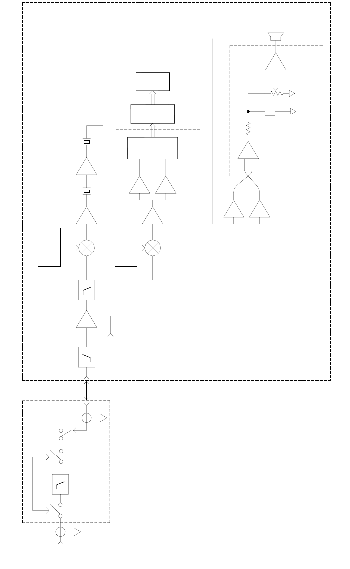
5.2.1 BLOCK DIAGRAM
Figure 5.2.1 shows the block diagram of the receive mode. The received RF signal
is routed from the rear panel antenna jack to a low pass filter selected by a relay
bank on the PA/Filter Assembly (ASY-0245-02). The output of the filter is routed
from J4 on the PA/Filter Assembly through a coaxial cable to the receiver input
circuitry on the Mainboard Assembly (ASY-0245-01). The signal is further
bandpass filtered to reject interfering signals and input to the RF
preamplifier/attenuator, Q2. In the "on" state, the amplifier provides some 3-4 dB of
low-noise preamplifier gain. In the "off" state, the stage becomes an attenuator that
provides approximately 10 dB of signal attenuation. The use of this switched gain
stage improves the weak signal sensitivity of the receiver and provides a front-end
attenuator that is used to insure that large signals do not swamp the ADC in the DSP
engine. The preamplifier/attenuator stage output is routed to the first mixer and the
signal is upconverted to the first IF at 45 MHz.
The 45 MHz IF signal passes through a low noise MMIC gain stage to a 4-pole
crystal "topping" filter with approximately 8 kHz bandwidth, a second MMIC
amplifier stage and a second two-pole crystal filter into the second mixer. In the
second mixer the signal is combined with the second Local Oscillator frequency of
45040 kHz. The mixer output signal is buffered by low-noise amplifier U3,
converted to a push-pull signal by U5 and then applied to the input of the A/D
converter U34. U34 digitizes the signal and passes it to the DSP engine, which
provides all baseband filtering, fine-tuning, demodulation and AGC functions. The
audio signal is converted to balanced format for transmission over the SEABUSS
audio lines to the Front Panel/Controller board (ASY-0245-03). The Controller
provides squelch processing, volume control and a speaker amplifier.
5.2.2 RECEIVE RF CIRCUITRY AND FIRST MIXER
As previously discussed, an incoming signal is first passed through some shared
circuitry on the PA/Filter Board (ASY-0245-02). This consists of a bandswitched
array of low pass filters, a T/R relay and a PIN diode signal limiter which prevents
damage to receiver input circuitry in the presence of extremely large signals. The
received signal is then sent through a coaxial cable to the receiver input on the
Mainboard Assembly (ASY-0245-01). On the Mainboard, a high-pass filter
consisting of C1, L1 and C7 further filters the signal.
Diode CR1 is forward biased in the receive mode from the +12VRX rail and
reversed biased in the transmit mode from the +12VTX rail through CR2. This T/R
switching circuitry provides extra isolation between the low-level transmitter signal
and any signal leakage through the PA/Filter Board T/R switches. From CR1, the
received signal passes through a low-pass filter (C5, L2 and C6) to the
preamplifier/attenuator stage. This stage is a low noise, low gain (+4 dB) broadband
common-gate JFET amplifier. A gain step is provided by switching the
preamplifier supply voltage on and off through Q6. When Q6 is OFF, the stage
ta8man.doc Page 5-4 FCCID: BZ6SEA245
becomes an attenuator with a loss of approximately 10 dB. The output of the
preamplifier is then applied to double-balanced mixer MIX1. The use of a hot
carrier diode mixer assures minimal cross modulation and intermodulation
distortion in the receiver front end.
5.2.3 THE 45 MHz IF
The output from mixer MIX1 contains the desired signal upconverted to 45 MHz.
This signal is amplified by a low noise, high dynamic range MMIC amplifier that
establishes a good low noise 50-ohm termination for the mixer. Output of the first
IF amplifier is filtered by FIL1, a four-pole monolithic crystal filter of approximately
8 kHz bandwidth. This is the "topping" filter, which serves to remove the unwanted
secondary image, RF, and LO leakage as well as other unwanted upconverted HF
signals that fall outside the filter bandwidth. Following the topping filter is a second
MMIC amplifier stage and a second 2-pole filter. The total gain between the
receiver input and the 45 MHz output is approximately 12 dB. The maximum
allowable input signal with preamplifier on is approximately -3 dBm. Switching in
the attenuator raises this level to approximately +10 dBm.
5.2.4 THE SECOND MIXER/POST AMPLIFIER
The second mixer converts the 45 MHz IF signal down to the second IF frequency
of approximately 40 kHz. This mixer is a +13 dBm type, necessary to handle the
somewhat higher signal levels present at this point. Following the mixer, the signal
is passed through a low noise operational amplifier with a stage gain of 10 to a
phase splitter circuit with stage gain of unity. The phase splitter output drives the
differentially configured A/D input.
5.2.5 THE A/D CONVERTER
In IF/DSP receivers, system performance is highly dependent upon the
characteristics of the A/D converter that moves the signal from the analog to the
digital realm. In the SEA 245, A/D Converter U34 is a 24-bit, 96 kHz stereo ADC
with a dynamic range of 110 dB and greater than 100 dB signal-to-noise ratio. The
inputs to the ADC are full differential and the chip includes a reference filter and a
digital decimation filter, which minimizes requirements for anti-aliasing filtering.
The 40 kHz second IF signal from the main receiver and the 14.583 kHz second IF
signal from the 2187.5 kHz monitor receiver are each connected to one of the stereo
inputs of the ADC. The resulting digitized signals are then passed on to the system
DSP that is located on the CPU Board (ASY-0245-04).
5.2.6 THE CODEC
The CODEC is part of the CPU Board Assembly (ASY-0245-04) and uses AC'97
REV 1.03 architecture in a 18-bit sigma/delta configuration. The CODEC contains
both an A/D and a D/A converter. The A/D converter is used to convert transmitter
baseband signals into a digital bit stream suitable for processing in the DSP.

ta8man.doc Page 5-5 FCCID: BZ6SEA245
The D/A converter works in both receive and transmit modes. While receiving,
digitally processed receiver signals from the DSP engine are converted back into the
analog realm for processing through the amplifier/loudspeaker system. When
transmitting, digitally processed (and generated) baseband signals from the DSP
engine become the analog input signals to I/Q modulator chip U6 on the Mainboard
Assembly.
5.2.7 THE DIGITAL SIGNAL PROCESSOR
The main DSP engine in the SEA 245 consists of U7 on the CPU Board Assembly.
This is a TMS320VC5402, a specialized type of microprocessor which includes
such features as a 40-bit ALU, data bus with Bus-Holder feature, extended
addressing mode for 1Mx16-bit maximum external program space and many other
specialized features intended to facilitate the specialized math functions necessary
for DSP.
In the SEA 245, the DSP circuitry and firmware perform most of the signal
processing functions necessary to convert a radio signal into an audio signal and
vice-versa. These functions include frequency conversion, filtering, demodulation
and gain control in the receive mode and baseband signal processing, filtering and
generation in the transmit mode.
Since the DSP engine is actually a highly specialized type of microprocessor many,
indeed most, of the characteristics of the receiver and transmitter functions are
controlled by firmware algorithms embedded in the CPU Board memory. It is thus
possible to use the same system digital hardware to generate (and demodulate) voice
signals, TELEX signals, Digital Selective Calling signals or essentially any signal
format up to the bandwidth limitations of the system analog hardware. Receiver
AGC characteristics, transmitter bandwidth shaping and ALC functions are all
determined in firmware.
5.2.8 THE RECEIVER AGC SYSTEM
There is only one variable gain element in the receiver AGC system, JFET
preamplifier Q2. The amplifier passes signals whether or not it is enabled but, when
disabled, there is approximately 10 dB of attenuation with respect to the enabled
state. The actual AGC parameters are determined by the DSP algorithm and are
tailored to suit the mode selected. When receiving SSB signals, the AGC has the
usual fast attack-slow release characteristics suitable for SSB. The DSP software
monitors signal level and disables the preamplifier when necessary to protect the
A/D input from overload.
5.2.9 THE RECEIVER AUDIO CIRCUITY
The received signal is processed through the DSP engine and converted to an audio
baseband signal in the system CODEC. This signal then exits the CPU Board as the
SPKR.AF signal on pin 19 of J3 on the Mainboard and then passes through audio
gate U30C to the audio SEABUSS driver stage consisting of U31B and U31C.
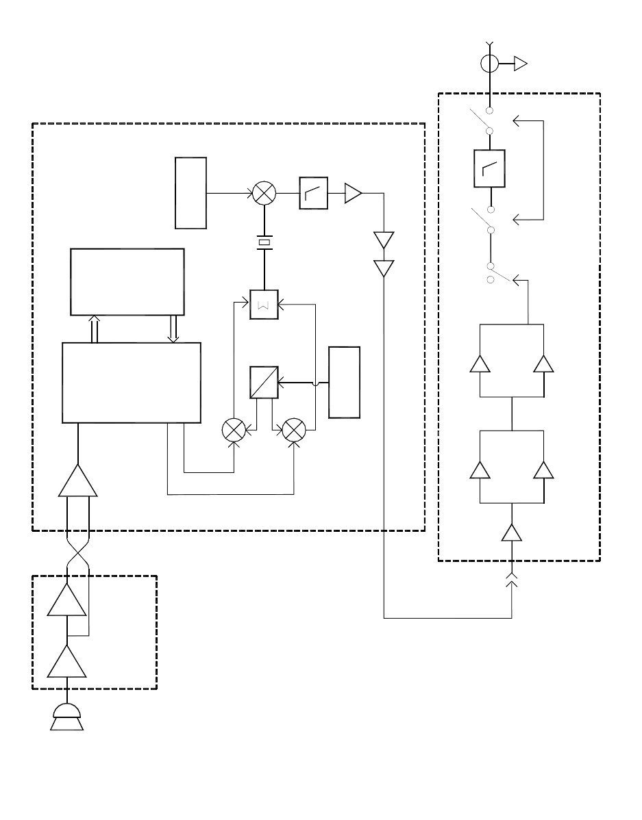
ta8man.doc Page 5-6 FCCID: BZ6SEA245
Transmitter Block Diagram
Figure 5.3.1
SEA 245
I
MIC
U10/DC
CONTROLLER
ASY-0245-03
U31A
DSP
U1
CODEC
U7
45-75 MHz
1st LO
Q
MAINBOARD
ASY-0245-01
PA/FILTER
Q1
Q2
Q3
45.016 MHz
90°
2nd LO
Q6
Q7
LOW
PASS
Q3
45MHz
FL1
Q5 Q4
MIX-1
TX/RX
PA/FILTER
ASY-0245-02
BAND SELECT
ANT
ta8man.doc Page 5-7 FCCID: BZ6SEA245
The audio signal then leaves the Mainboard Assembly (ASY-0245-01) as a 600
ohm balanced 0 dBm level and is received by the SEABUSS audio receiver in the
Front Panel/Controller Assembly consisting of balanced line amplifier U10A.
After passing through U10A, the signal is then sent to the VOLUME control and the
squelch limiter U8A and U8B. The signal from the VOLUME control wiper then
goes to AF Power Amplifier U14 where it is amplified to a 4-Watt level and is then
sent to the loudspeaker.
The limited audio signal from U8A is sent to an input of the Controller
microprocessor (U1) where it is used to generate the SQL signal. An algorithm in
U1 senses the presence (or absence) of a voice signal in the limited audio signal and,
when the Squelch function is activated, generates a SQL OUT signal. The SQL
OUT signal is used to turn on the squelch gate transistor Q6 to silence the
loudspeaker.
5.3 THE TRANSMITTER
5.3.1 BLOCK DIAGRAM
Figure 5.3.1 shows the block diagram of the SEA 245 in the transmit mode.
Microphone audio is amplified and converted to a balanced format for transmission
from the Front Panel/Controller Assembly to the Mainboard Assembly (ASY-0245-
01) via the SEAbuss audio lines. On the -01 board it is converted back to
unbalanced format and then digitally sampled by CODEC U1 on the CPU board
(ASY-0245-04). The CODEC transfers the data serially to the DSP, U7. The DSP
generates a SSB signal at the (nominal) subcarrier frequency of 16 kHz. The
CODEC converts the digital sample stream back to analog format. The resulting I
and Q SSB signals are fed back to the Mainboard and into the inputs of quadrature
modulator U6. The modulator mixes the I and Q signals with in-phase and
quadrature 45.016 MHz local oscillator signals. This results in a single sideband
signal at the 45 MHz intermediate frequency. This IF signal is passed through the
bilateral 45 MHz crystal filter into the IF port of mixer MIX1. This mixer
downconverts the IF signal into the MF/HF RF band. The RF signal is low-pass
filtered and amplified before being passed on to the PA/Filter Assembly (ASY-
0245-02) via a coaxial cable. Transmitter preamplifier Q1 boosts the signal level
sufficiently to drive the push-pull driver stage consisting of Q2 and Q3. The driver
output is then routed to the push-pull power amplifiers, Q6 and Q7. The output of
the amplifier is then routed through the T/R relay to a low pass filter that is relay
selected for the desired band of operation. The filtered output is fed to the antenna
jack on the SEA 245 rear panel.
5.3.2 THE MICROPHONE AUDIO CIRCUITRY
The 600 ohm dynamic microphone output is terminated by 620 ohm resistor R8 and
then passes through R94 and C13X to the input of the amplifier/phase splitter stage
ta8man.doc Page 5-8 FCCID: BZ6SEA245
consisting of operational amplifiers U10C and U10D. MOSFET Q5 is connected
between the junction of R94 and C13X and ground and serves to mute the
microphone circuitry in the receive mode. The balanced audio output from U10C
and U10D passes through analog gates U13A and U13D to the SEAbuss audio line.
The SEABUSS audio interconnection between the Front Panel/Controller
Assembly (ASY-0245-03) and the Mainboard Assembly (ASY-0245-01) is through
the 8-pin ribbon cable between P2 on the Controller board and J4 on the Mainboard.
These 8-pin DIP interconnections constitute an internal SEABUSS interface
between the two assemblies.
5.3.3 THE AUDIO LINE RECEIVER/TRANSMITTERS
SEABUSS audio is bidirectional and passes through audio line receiver/transmitters
at both ends of the path.
The receiver/transmitter circuitry consists of a balanced input line receiver and a
balanced output line driver or transmitter. The line driver is connected to the
SEAbuss(c) line through analog gates. These gates disconnect the line driver from
the SEABUSS when the receiver/transmitter is in the receive mode. In the receive
mode, balanced audio is presented to the input of an operational amplifier connected
as a differential amplifier. Balanced operation permits a high degree of common
mode rejection, insuring good noise rejection. The output of the line receiver is
unbalanced audio which is then passed on to the internal radiotelephone circuitry.
When the receiver/transmitter circuitry is in the transmit mode, the analog gates are
turned on, connecting the balanced output of the two amplifier line driver to the
SEABUSS.
SEABUSS audio level is nominally 2 volts peak-to-peak balanced (0 dBm).
5.3.4 THE CODEC AND DIGITAL SIGNAL PROCESSOR
CODEC, U1, digitizes audio from the microphone circuitry at a rate of 96
kilosamples each second. The samples are transferred to the DSP U7 for
processing. The DSP performs audio processing to maintain a relatively uniform
audio level and to reduce the peak-to-average ratio of the audio. This facilitates
more efficient use of the RF power amplifier. The audio is also bandpass filtered to
remove unwanted components, particularly above 2900 Hz. The audio is then
converted to a single sideband signal at the (nominal 16 kHz) subcarrier frequency.
This SSB signal is then passed through the CODEC and converted to I and Q analog
signals.
5.3.5 THE QUADRATURE MODULATOR
The I and Q signals from the CODEC are sent to quadrature modulator U6 on the
Mainboard. This modulator consists of a PLL based LO phase shifter, two mixers
and a combiner. A 45.016 MHz local oscillator (LO) signal from the synthesizer is
AC coupled into the modulator. The internal PLL circuit regenerates the 45.016
ta8man.doc Page 5-9 FCCID: BZ6SEA245
MHz LO and produces two 45.016 MHz LO signals with a 90 degree phase
differential. These are used as the two local oscillators for the mixers. One is
mixed with the I component and the other is mixed with the Q component. The two
mixer outputs are summed to complete the single sideband mixer. In the summer
the desired sideband adds constructively while the undesired sideband cancels out,
producing a single sideband signal with a center frequency of 45 MHz. A DC bias
network with three trimpots (R77, R78, and R85) allows adjustment of opposite
(image) sideband and carrier suppression.
5.3.6 45 MHz IF AND SIGNAL MIXER
The 45 MHz signal from the quadrature modulator passes through switching
diode/attenuator CR6 to topping filter FIL1A/FIL1B. When in the transmit mode,
CR6 is biased on by the +12VTX rail through resistors R48 and R66. Bias current
is approximately 10 mA, resulting in a low loss switch. Monolithic filter
FIL1A/FIL1B is matched to the low impedances of the quadrature modulator and
mixer by the two "L" networks, L10/C39 and L9/C38. The filter output is passed
through CR5 to a attenuator consisting of R34, R35 and R36 and then through CR4
to the IF port of MIX1
5.3.7 THE LOW PASS FILTER AND TRANSMITTER PREAMPLIER
The downconverted transmitter signal from MIX1 is passed through a seven section
elliptical function low pass filter which provides some 50 dB of rejection for the
image and IF frequencies above 30 MHz. The filtered MF/HF signal is then passed
through diode switch CR3 to the input of the transmitter preamplifier. L6, A 27 μH
choke, serves as a simple high pass filter to restrict signal into the preamplifier to the
MF/HF spectrum. The transmitter preamplifier is a two-stage wide band amplifier.
The first stage consists of transistors Q3 and Q4 in a negative feedback voltage
amplifier. The output of this stage is taken from the low impedance emitter of Q4
and further amplified by Q5. Q5 is a transformer coupled power amplifier which is
used to boost the power output level of the SSB signal to the approximately 4 mW
(+6 dBm) required by the PA/Filter Assembly (ASY-0245-02). The signal exits the
Main Board via coaxial cable and enters the PA/Filter board on J1.
5.3.8 THE TRANSMITTER PREDRIVER
The low level transmitter signal is routed from J1 through a 3 dB pad and a
wideband transformer (T1) to the base of Q1. Q1 is a 2N3866 connected in the
common emitter configuration and is transformer coupled to the push-pull driver
stage. Bias for Q1 is provided by the base resistor network with R6 used to adjust
the idling (no signal) current in the device to 60 mA (0.275 volts across R7/R8).
The emitter resistor (R7/R8) is used together with press-on heat sink to provide
thermal stability for Q1.
ta8man.doc Page 5-10 FCCID: BZ6SEA245
5.3.9 THE TRANSMITTER DRIVER
Transistors Q2 and Q3 are small plastic RF power devices connected as a push-pull
common emitter amplifier. Transformer T2 provides push-pull base drive from the
predriver, while transformers T3 and T4 provide DC power isolation and collector
to load impedance matching, respectively. Gain/bandwidth compensation is
provided by the collector/base feedback networks and the various peaking capacitors
and terminating resistors. Temperature tracking bias is provided for Q2 and Q3 by
the circuitry associated with Q4 and Q5. Q4 is a small silicon power transistor
connected as a voltage amplifier and buffered by power emitter follower Q5. The
current in Q4 is proportional to temperature. This causes the collector voltage to
drop as heat sink temperature rises. The collector voltage is the source of base drive
for the bias buffer emitter follower Q5. Bias current for Q2 and Q3 is adjusted to
140 mA by the potentiometer, R14, in the emitter circuit of Q4. Collector voltage
for Q4 is derived from the +10VTX bus, while collector voltage for Q5 is derived
from the +12VTX rail.
5.3.10 THE TRANSMITTER POWER AMPLIFIER
The power amplifier in the SEA 245 is a push-pull common emitter design with a
temperature stabilized bias source. The amplifier runs from the +24 volt input and
has the collector voltage present at all times. The amplifier is activated by turning
on the various bias supplies when in the transmit mode.
Since the +24 volt power source is isolated from the chassis, the power amplifier
bias generator must be powered from the +24 volt rail. The bias generator circuitry
consists of Q8, Q9 and regulator U4. +24 volt power for U4 and Q8 is switched by
the +12VTX rail through Q12 by optical isolator U5. When the +12VTX rail is
high U5 turns on Q12, energizing the bias generator circuitry. Q8 serves as a power
emitter follower to buffer the voltage generated by the temperature-tracking
amplifier, Q9. Q9 is a small power transistor that is thermally linked to the power
amplifier heat sink. To insure stability in the presence of varying line voltages, the
collector voltage for Q9 is obtained from 9 volt regulator U4. R28 permits
adjustment of the idling (no signal) current in Q6 and Q7 to 150 mA.
5.3.11 THE OUTPUT LOW PASS FILTERS
Five low pass filters are provided to cover the frequency range from 1.6 - 30 MHz.
Note that the highest frequency filter, which covers the-26 - 30 MHz spectrum, is a
3-pole elliptical function design, while the lower frequency filters are 7 pole
elliptical function types. This is possible because of the natural drop in spurious
outputs from the power amplifier at higher frequencies. Filter selection is through
small power relays, which are operated by the Mainboard controller computer
through a serially loaded relay driver consisting of shift register U2 and buffer-
driver U3.
ta8man.doc Page 5-11 FCCID: BZ6SEA245
5.3.12 THE ALC CIRCUITRY
The transmitter ALC circuitry is DSP based. The control signals for the ALC
system are derived from the dual directional coupler consisting of transformers T13
and T14 and termination resistors R44, R47 and R48. The forward power signal is
detected by CR3 and scaled by resistors R49 and R50 before being buffered by
U1B. The reflected power signal is detected by CR4 and buffered by U1A. The
buffered analog voltages corresponding to forward and reflected power levels are
then routed through the Mainboard to A/D converter inputs on the CPU board
microprocessor, U5.
5.4 THE MASTER CLOCK OSCILLATOR AND SYNTHESIZER SYSTEM
5.4.1 BLOCK DIAGRAM
Figure 5.4.1 shows the block diagram of the local oscillator system of the SEA 245.
The block diagram illustrates a total of two synthesizers. The first local oscillator
operates from 45 to 75 MHz and uses three bandswitched VCOs. These are
controlled by synthesizer chip, U21, which contains a dual modulus divide-by-N
counter, a variable modulus reference counter and a phase detector. The basic
reference rate for the phase detector is 8 kHz, which sets the "coarse" step size for
the first local oscillator to 4 kHz. (The VCO signal tunes from 90 to 150 MHz and
is divided by two before being applied to the first mixer.)
The second local oscillator synthesizer operates at 45.040 MHz with a reference rate
of 8 kHz.
5.4.2 THE MASTER CLOCK OSCILLATOR
Primary frequency control is maintained through a master temperature-stable crystal
oscillator (TCXO) operating at 12.288 MHz. Clock stability is achieved through a
combination of temperature control and temperature compensation. The Master
Clock Oscillator crystal Y2 is mounted in a proportional oven to insure stability.
Unbuffered HCMOS U9 and U25 gates are used for both oscillator and buffer
amplifier functions. Trimmer capacitor C56 is used to set the clock frequency.
5.4.3 THE FIRST LOCAL OSCILLATOR SYNTHESIZER
The first LO synthesizer consists of three switched VCOs, a buffer amplifier and a
phase locked loop circuit. The synthesizer generates local oscillator frequencies
from 45.4 - 75.0 MHz corresponding to operating frequencies of 0.4 - 30.0 MHz.
The oscillators themselves operate at twice the desired output frequency, however.
Operation of a typical VCO is described below. Q23 is configured as a Colpitts
oscillator with inductor L35 and varactor diode CR15 serving as the frequency
determining elements. Q24 buffers the VCO to prevent load pulling. These
components make up the highest frequency VCO, which tunes from approximately
ta8man.doc Page 5-12 FCCID: BZ6SEA245
130 to 150 MHz.
Switch transistors Q16, Q17 and Q18 provide power to the selected VCO. The base
of Q18 is pulled low through R146 supplying 10 volts to the HIGHBAND VCO,
Q23-Q24. When the MIDBAND VCO is selected, Q13 will be turned on by a high
on pin 16 of U21. This will pull the base of Q17 low, energizing Q21 and Q22. At
the same time the base of Q18 is pulled high through diode CR10 switching OFF
the HIGHBAND VCO. Similarly, selection of the LOWBAND VCO is
accomplished by a high on pin 15 of U21, which turns on Q14/Q16, supplying
power to Q19/Q20 and
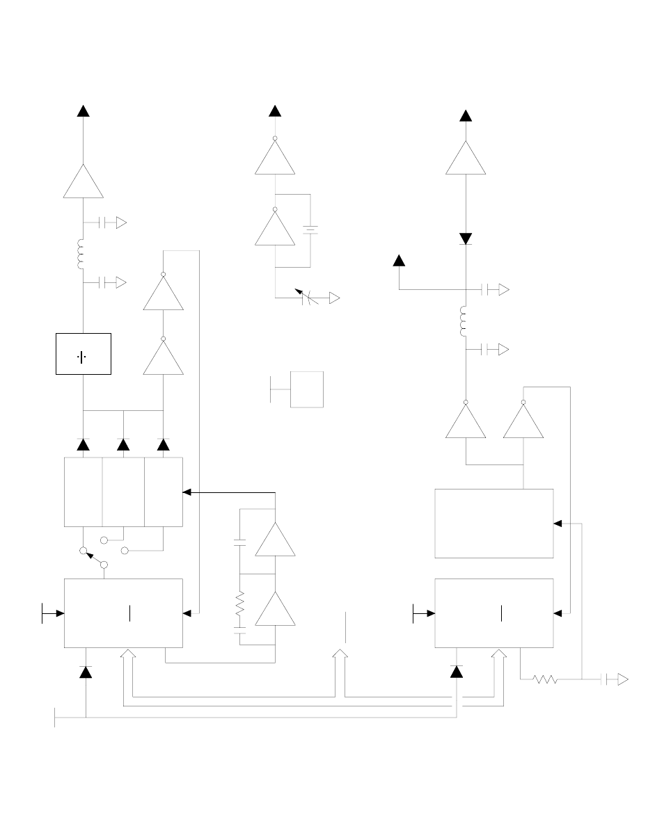
ta8man.doc Page 5-13 FCCID: BZ6SEA245
SEA 245
Synthesizer Block Diagram
Figure 5.4.1
U21
12.288MHz
Q19,Q20
SWITCH
Q21,Q22
Q23,Q24
BAND
SYNDATA
CS2
SYNCLK
UNLK
U17
SYNCLK
CS1
SYNDATA
12.288MHz
U22A/B
TO CPU
U24
U39A/B
90-150MHz
245-75MHz
1st LO
TO MIX-1
U23
Q12
Q13
U18A
U18B CR24
45.04/45.016MHz
Q33
TX ENABLE
45.04MHz
TO MIX-2
2nd LO
U25
MASTER CLK
12.288MHz
TRIM
CLK
Y2
U9
C56
+12VS
OVE1
45.016MHz
TO I/Q MODULATOR, U6
ta8man.doc Page 5-14 FCCID: BZ6SEA245
holding OFF the HIGHBAND VCO through diode CR10. Steering diodes CR17
and CR18 are used to provide isolation between the two OFF VCOs and the active
output.
The output from the selected VCO is passed through prescaler, U23 where the
signal is divided by two. The prescaler output is buffered by MMIC, U24, before
being sent to the first mixer. The VCO output is also passed through dual buffer
amplifiers U39A and U39B. The output signal from U39B provides the VCO signal
to the synthesizer chip U21. Using separate amplifiers in this fashion improves the
isolation between the receiver mixer circuitry and the input to the synthesizer chip.
Serially loaded PLL chip U21 provides a reference counter, divide-by-N counter, a
phase/frequency detector and the VCO control register. The PLL reference
frequency is derived from the 12.288 MHz Master Clock. Loop filtering and level
shifting of the PLL phase detector output is accomplished by active filters U22A/B.
5.4.4 THE SECOND LOCAL OSCILLATOR SYNTHESIZER
The second local oscillator synthesizer consists of PLL chip U17, 45.040 MHz
Colpitts oscillator FET Q12, and buffer amplifier Q13, U18A, U18B and Q33.
Buffer amplifier U18A provides a sample of the 45.040 MHz VCO signal for the
synthesizer chip while U18B provides 45.040 MHz drive for the second mixer.
5.5 THE 2187.5 kHz MONITOR RECEIVER
5.5.1 BLOCK DIAGRAM
Figure 5.5.1 shows the block diagram of the 2187.5 kHz monitor receiver, required
for GMDSS applications is Sea Area 2. The receiver is a single channel, dual
conversion design which uses a single crystal to provide both conversion signals.
The first IF frequency is 455 kHz, the second IF frequency is nominally 14.583 kHz.
As in the SEA 245 Main Receiver, the DSP engine provides all channel selectivity,
signal demodulation, and AGC.
5.5.2 RECEIVER RF CIRCUITRY AND FIRST MIXER
Antenna input to the 2187.5 monitor receiver is on pins 13 (signal) and 14 (ground)
of the rear panel Accessory Connector. The impedance is 50 ohms and provisions
have been made to support the SEA 7002 Active Antenna, should this be desired.
The RF signal first passes through a high pass filter and a low pass filter to Q9, the
preamplifier. The preamplifier is a grounded-gate JFET with tuned drain circuit.
The nominal gain of this stage is about 8 dB with the drain voltage on. As in the
main receiver, switching the drain voltage off under control of the AGC software in
the DSP provides a gain step. The combination of the front end 5-section low pass
filter and the low pass response of the preamplifier drain circuitry combine to
provide the receiver with better than 75 dB rejection of the 3097.5 kHz primary
ta8man.doc Page 5-15 FCCID: BZ6SEA245
image.
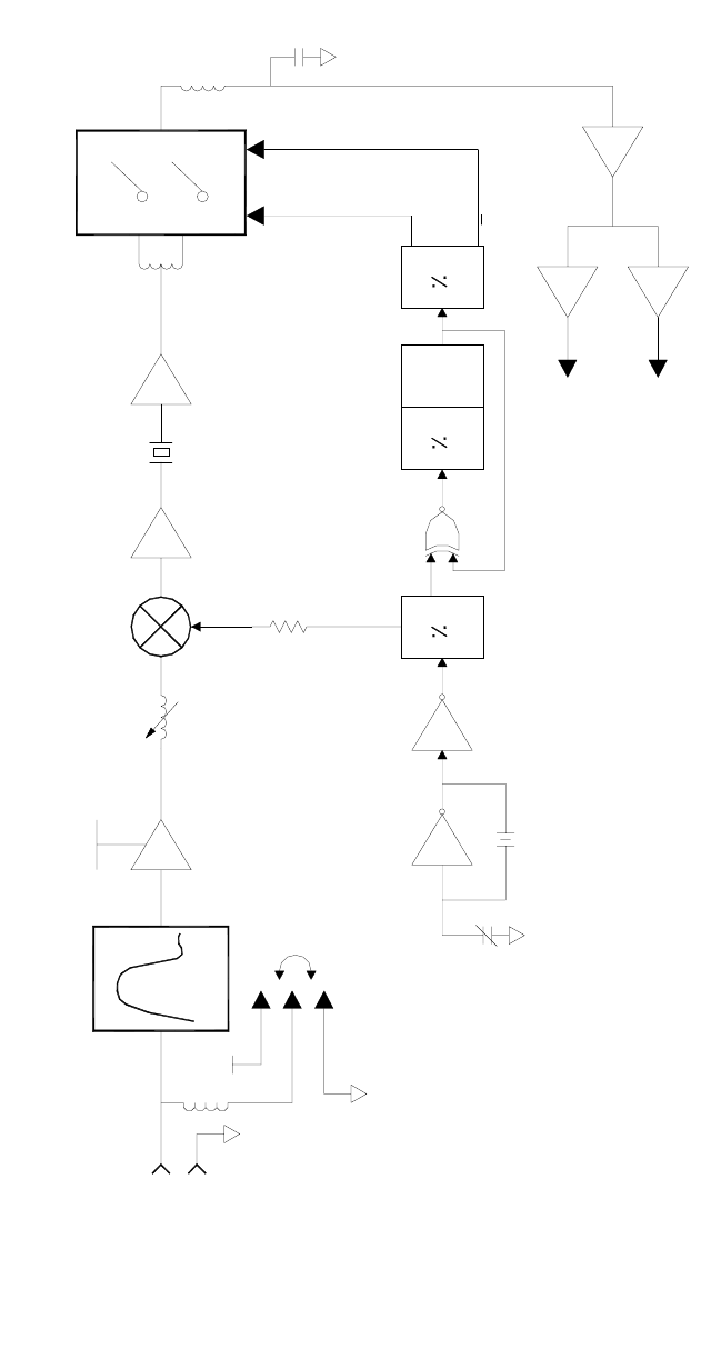
ta8man.doc Page 5-16 FCCID: BZ6SEA245
Figure 5.5.1
SEA 245
2187.5 KHz MONITOR BLOCK DIAGRAM
FILTER
BANDPASS
ANTENNA
SEA 7002 or
2187.5KHz
+12VRX
Q9
GAIN CONTROL
L20
MIX-3 Q10 FL-3 Q11
MIX-4
L26
C107
U15
U7A/B
TO ADC @
14.583KHz
2
U10B
Q
Q
U10A
U12B
3
U12A
U13U14
C116
ADJ
CLK
Y1
5285.0 KHz 880.833 KHz
U11
2642.5 KHz
7002
ANT.
455KHz
2440.4167
KHz
ta8man.doc Page 5-17 FCCID: BZ6SEA245
The first mixer is a conventional +7 dBm double balanced type, which provides
excellent dynamic range in this application.
5.5.3 THE 455 kHz IF AMPLIFIER
The first 455 kHz IF amplifier is Q10, a grounded-gate JFET which provides some
gain and serves as a wideband 50 ohm termination for the mixer. The output from
the amplifier is passed through FL3, a 6-pole ceramic bandpass filter with a nominal
bandwidth of 4 kHz. Output from the filter is then passed through emitter follower
Q11 to the second mixer.
5.5.4 THE SECOND MIXER/POST AMPLIFIER
The second mixer is a double balanced commutation mixer, which uses a quad
HCMOS analog gate (U16) as the switching element. Push-pull signal drive is
provided to the two switch arms through a wideband transformer. (Note that two
gate elements are used in each switch arm.) Push-pull local oscillator drive is
applied to the switch actuator pins from the output of the local oscillator divider
chain. Both output arms of the switch are summed together, resulting in a double-
balanced switching mixer with excellent dynamic range and good local oscillator
balance.
Output from the mixer is passed through a low pass filter consisting of L26 and
C107 to a low noise operational amplifier stage with gain of 10 and a phase splitter,
which, as in the Main Receiver, drives the A/D input.
5.5.5 THE LOCAL OSCILLATOR CIRCUITRY
Both conversion oscillator frequencies are derived from the same crystal controlled
source in the following fashion. Crystal oscillator U14 operates at 5285.0 kHz. This
oscillator is temperature compensated and maintains a frequency stability of less
than ±4 ppm over the voltage and temperature range of the equipment. Trimmer
capacitor C116 is used to set the oscillator frequency to exactly 5285.0 kHz at TP10.
Output from the oscillator is buffered by gate U13 and then divided to 2642.5 kHz
by U12A. This signal is sent to both the first mixer and the second local oscillator
divider chain. The difference frequency between the first local oscillator and the
2187.5 kHz signal frequency is 455 kHz.
U11, U12B and U10A form a symmetrical divide-by-three counter. The resulting
880.3333 kHz signal is then further divided by two in U10B. The Q and notQ
outputs of U10B are at 440.4167 kHz and, when mixed in MIX-4 with the 455 kHz
IF signal, results in the 14.5833 kHz last IF frequency which is amplified by U3 and
U5A/B and then sent through the A/D converter to the DSP for further filtering and
demodulation.
ta8man.doc Page 5-18 FCCID: BZ6SEA245
5.6 THE POWER SUPPLY CIRCUIT
5.6.1 GENERAL
The basic supply voltage for the SEA 245 is a floating ground 24 Volt DC source.
Line voltage regulation of ±15% or better is required, with a current capacity of at
least 15-20 amperes. From this raw source are derived the necessary regulated
operating voltages for the SEA 245 circuitry.
5.6.2 BLOCK DIAGRAM
Figure 5.6.1 shows a simplified schematic diagram of the power supply circuitry.
Once the basic 24 Volt DC power is provided, it is connected to the set through the
heavy-duty power plug on the transceiver rear panel. A variety of internally
mounted fuses are provided to protect the set in the event of malfunction. The
primary line fuses are equipped with a polarity protection diode that will blow the
line fuses in the event of reversed line polarity.
As illustrated in Figure 5.6.1, the 24 Volt DC power from the rear panel mounted
connector passes through a ferrite line filter to the PA/Filter Board (ASY-0245-02)
where the power is distributed to the internal circuitry through fuses F1 and F2.
15 ampere fuse F1 serves to protect the circuitry associated with the output stage of
the power amplifier. 5 ampere fuse F2 protects the primary circuitry for the isolated
24/12 volt DC/DC converter which provides the regulated, chassis referenced, +12
volt rail. The +12 volt rail powers the low level circuitry in the SEA 245. Each fuse
is individually protected from reverse polarity by power diodes CR1 and CR2 and
each power rail is individually filtered by 470 μF capacitors C29 and C47. Note that
these rails are NOT switched. Power is present on the power amplifier module and
the DC/DC converter input AT ALL TIMES.
5 ampere fuse F3 protects the regulated +12 volt primary power distribution system
in the SEA 245. Capacitors C75, C76 and C78 serve as line filters. The fused,
filtered +12 volt regulated rail is designated the +12VSW line and is distributed to
the SEA 245 circuitry through pins 5 and 6 of J8 on the PA/Filter Assembly.
(Ground and negative rail use pins 7 and 8).
5.6.3 THE MAIN POWER CONTROL CIRCUITRY
The main power switch in the SEA 245 is the ON/OFF switch located on the front
panel VOLUME control. Wires from the switch connect to J9 on the PA board
(ASY-0245-02). When the front panel switch is closed by rotating the VOLUME
control to the right from the stop, a connection is made between J10 pins 1 and 3.
This turns the 24/12 volt DC/DC converter ON and powers up the +12VSW rail in
the SEA 245.
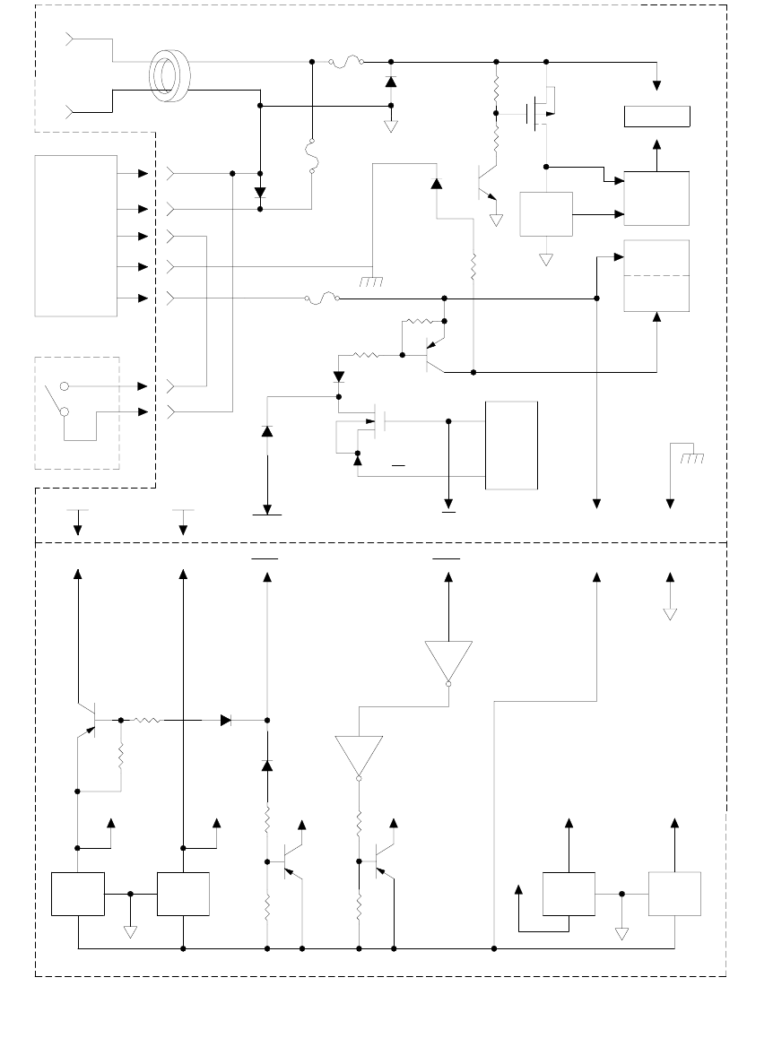
ta8man.doc Page 5-19 FCCID: BZ6SEA245
U36U38 U37
Power Distribution Block Diagram
Figure 5.6.1
SEA 245
Q26
12VSW
Q29
U35
Q6,Q7
-
+3.3V
+12TX(PA)
Q12
14
+10V
J6 13
J8
+10VTX
+10VTX
+5V
+5V
Q30
+12VRX
+12TX
+5V
Q28
9MAINBOARD
(ASY-0245-01)
TXINT
TXEN
10
RXEN
RX
+
ASY-0245-03
ON/OFF J9
+
-
CONTROL
2
1
3
-
DC/DC
24/12V
CONV.
5
4
J10
Q15
F3,5A
TX
U3
CHASSIS
PA GND
-12VSW
+12VSW
CR2
F2,5A
U4
+12VSW
~
U5
CHASSIS
5,6 7,8
GND
12VSW
+12VSW
PA/FILTER
CHASSIS
(ASY-0245-02)
+9V
Q8,Q9
BIAS
BIAS
J6
+24VDC
J7
+F1,15A
CR1
+24VCC
Q2,Q3
Q1,Q4,Q5
Q14
+5VAD
+5V

ta8man.doc Page 5-20 FCCID: BZ6SEA245
5.6.4 +10 VOLT REGULATOR AND THE +10VTX SWITCH
The internal +10V rails are derived from the +12VSW bus through regulator U38.
The +10VTX rail is generated by inverted switch Q27. Grounding the notTXEN
line will turn on Q27, enabling the +10VTX rail. The notTXEN line comes from
the PA/Filter Assembly through pin 9 of J6.
5.6.5 +12 VOLT RAIL AND THE +12VTX/+12VRX SWITCHES
Transistors Q26 on the mainboard generate the mainboard +12VTX rail. The
+12VTX rail is energized when the notTXEN line from pin 9 of J6 goes low,
switching Q26 on.
The +12VRX rail is energized when the notRXEN line from pin 10 of J6 goes low.
This turns Q30 off which turns Q28 on, switching Q29 on.
The use of transistor switches to generate the TX and RX rails eliminates any
problems with relay contacts or T/R timing.
5.6.6 +5 VOLT REGULATORS
The +5 volt rail for the Mainboard Assembly and the PA/Filter Assembly is derived
from the +12VSW rail through regulator U37.
In the Front Panel/Controller Assembly (ASY-0245-03) a separate 5 volt regulator,
U16, provides the regulated rail for the controller circuitry. Note that the controller
+12VSW rail comes through the standard SEABUSS interconnection.
5.6.7 +3.3 VOLT REGULATOR
U36 on the Mainboard Assembly provides the +3.3V rail which is used in the
CPU/DSP Board (ASY-0245-04) to power the main control computer hardware.
5.6.8 +12VTX RAIL
The transmitter predriver circuitry and the bias systems for the transmitter driver are
supplied with a relatively high current +12VTX rail through Q14. Q14 is a PNP
power transistor, operated as an inverted switch. Base drive for Q14 is provided by
the INTERLOCKED notTX line. This line is obtained through the "safety clamp'
transistor, Q15, from the notTX and notRX ports generated by the controller
computer through the shift register U2 and the buffer chip, U3. When the notTX
port from pin 16 of U3 is LOW and the notRX port from pin 5 of U2 is HIGH, the
INTERLOCKED notTX line is LOW. This will cause Q14 to be ON, energizing
the +12VTX rail.
Note that the INTERLOCKED notTX line is also used to control Q26 and Q27, the
+12VTX and +10VTX switch transistors respectively, on the Mainboard Assembly.
The use of the INTERLOCKED NOT TX line in this fashion prevents the
simultaneous application of +12VTX and +12VRX to the low level transceiver
ta8man.doc Page 5-21 FCCID: BZ6SEA245
circuitry.
5.6.9 THE +24VTX RAIL AND PA BIAS SYSTEM
Bias for the PA output transistors is generated from the +24VTX rail. Since the
entire +24 volt power source is isolated from the chassis, an optical isolator, U5 on
the PA/Filter Assembly (ASY-0245-02) is used to switch on a P-channel FET (Q12)
when the +12VTX rail is energized. This +24VTX line is then used to power bias
regulator transistor Q8 and the +9V PA bias supply regulator U4. The output from
U4 powers bias tracking amplifier transistor Q9. Q9 is a small power device which
is bonded to the same heat sink as the RF power transistors to provide thermal
feedback.
5.7 THE MAINBOARD CONTROLLER AND DSP PROCESSORS
5.7.1 GENERAL
The Mainboard microcontroller and digital signal processor (DSP) are contained on
a separate assembly (ASY-0245-04). The microcontroller is a Motorola
MC68C812A4 operating from a 6.144 MHz clock. This is a low voltage (3.3V) 16-
bit processor with two asynchronous serial ports, a serial peripheral interface (SPI),
a timer and pulse accumulator module, an 8-channel 8-bit A/D converter, 1 Kbyte of
RAM, 4 Kbytes of EEPROM and memory expansion logic with chip selects. It also
has many bidirectional ports for general purpose I/O. The DSP is a TI
TMS32OVC5402. This is a 32-bit fixed-point DSP capable of 100 MIPS operation.
It includes 16 Kwords (16-bit) of internal RAM, two sophisticated multichannel
serial ports and a parallel host port interface.
5.7.2 BLOCK DIAGRAM
Figure 5.7.1 shows a block diagram of the processor assembly.
5.7.3 CLOCK DISTRIBUTION
The 12.288 MHz master clock is supplied through P2 to the processor assembly
(ASY-0245-04). U11A divides this clock by two to provide a 6.144 MHz clock to
the microcontroller, U5. U9 buffers the clock and converts it to a 1.8 volt level
suitable for the DSP, U7. The DSP has an internal PLL which generates a 98.304
MHz clock phase locked to the 12.288 MHz reference. The 98.304 MHz clock is
used as the cycle clock for the DSP and is also divided by 4 by U10 to produce a
24.576 MHz clock for the CODEC, U1. This clock divider can be reset by the DSP
in order to insure a known phase relationship between the CODEC clock and the
DSP clock. This is necessary for reliable communication between the CODEC and
the DSP.
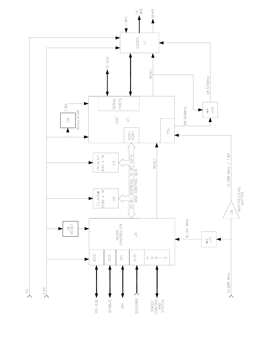
ta8man.doc Page 5-22 FCCID: BZ6SEA245
SEA 245 Processor Assembly
Block Diagram
Figure 5.7.1
ta8man.doc Page 5-23 FCCID: BZ6SEA245
5.7.4 MICROCONTROLLER OPERATION
Reset generator, U8 provides a reset pulse to microcontroller U5 at startup or if
there is a dip in the power supply. At startup the microcontroller has access only to
the internal resources. It runs software contained in the internal EEPROM. This
software configures the chip and either boots a program from the RS-232 port
(Useful for service and reprogramming functions) or transfers control to the flash
memory. The flash memory contains most of the software for running the radio.
The radio channel list also resides in flash as well as software to be downloaded to
the DSP. A 64 kword external RAM is provided for workspace and stack space.
Additional memory for scratchpad channel storage and radio configuration
parameters is contained in the nonvolatile internal EEPROM. The microcontroller
may also communicate with the DSP as a memory-mapped device on the bus.
The processor has two asynchronous serial interfaces (SCI's). SCI0 is used to
provide an RS-232 interface to the radio which can be used for computer control or
for reprogramming the flash memory. SCI1 is used to provide a SEABUSS
interface to the front panel or a remote controller. The processor also has a serial
peripheral interface (SPI) which is used to communicate with the synthesizers as
well as a shift register which provides control signals to the PA/Filter Assembly.
The processor has an 8-channel analog to digital converter port. Not all of these
A/D converter channels are in use but some of them are used to read temperature
sensors, power sensors and synthesizer lock detection signal ports.
Finally there are quite a few general purpose I/O ports used to control the radio. For
example these are used to control gates to route audio signals, to communicate with
an Automatic Antenna Tuner, to control receiver gain steps, to switch the cooling
fan and the reset the DSP.
5.7.5 DSP OPERATION
At startup the DSP, U7, is reset by a port signal from the microcontroller, U5. The
microcontroller then transfers the firmware from the flash memory, U4, to the DSP
via the host port interface on the microcontroller's bus. This firmware runs out of
the DSP's internal RAM.
The DSP has two serial ports. One of these is used to communicate with the
previously described A/D converter on the Mainboard. This stereo 24-bit converter
samples signals from the Main Receiver and the Watch Receiver 96000 times per
second. During each sample two 24-bit words (One for each receiver) are
transferred over the serial port to the DSP. The DSP generates the 96KHz clock
which provides a framing signal to the A/D to select between the two channels. The
other serial port is connected to the CODEC, U1, which is described further below.
The interface is similar to the A/D interface but the sample rate is 48 KHz.
The operation of the DSP depends on whether the radio is receiving or transmitting.
When receiving the DSP reads receiver samples from the A/D. The digitized SSB
ta8man.doc Page 5-24 FCCID: BZ6SEA245
samples are processed to convert them to the audio band, filter out undesired signals
and provide gain control and noise blanking. Watch Receiver signals are also FSK
demodulated in order to detect Digital Selective Calling (DSC) data. Audio samples
from the Main Receiver are passed to the speaker audio circuit through the CODEC
monophonic output. DSC data is passed to the microcontroller over the host port
for further data decoding. In transmit mode microphone audio samples are read by
the DSP from the CODEC, U1. the DSP performs speech processing on these
samples and converts them to inphase and quadrature signals at an IF of
approximately 15 KHz. These I and Q samples are transferred to the I/Q Modulator
through the CODEC.
In both transmit and receive modes, the DSP also communicates regularly with the
microcontroller over the host port. In receive mode the DSP regularly sends gain
information to the microcontroller as well as DSC data. In the transmit mode the
DSP must obtain power sensor data from the microcontroller in order to implement
Automatic power Level Control (ALC). The DSP also receives mode information
from the microcontroller which determines operating parameters of the DSC such
as PTT status, transmitter power level and receiver bandwidth.
5.7.6 CODEC OPERATION
U1 is an AC '97 compliant 18-bit stereo CODEC operating with a 48 KHz sample
rate. On board multiplexers can select between two stereo inputs and three mono
inputs. It also has selectable stereo or mono outputs. Each channel has independent
gain and mute controls. All of the control and status as well as the stereo input and
output sample data is passed over the serial connection to the DSP. the stereo
output is used for transmit I and Q samples for the modulator. The mono output is
used for speaker audio. Two of the inputs are used for microphone audio and an
alternate low level audio input. The other input channels are not used.
ta8man.doc Page 6-1 FCCID: BZ6SEA245
6 THE SEA 245 FRONT PANEL/CONTROLLER SYSTEM
6.1 GENERAL
The SEA 245 Front Panel/Controller unit is a complete SEABUSS controller and is
designed in such a manner as to permit direct installation on the front of a standard
SEA 245 as well as in remote installations. The SEA 245 will support a SINGLE
remote controller and a SEABUSS compatible Antenna Tuner such as the SEA
1631. The maximum TOTAL length of SEABUSS cable not to exceed 200 feet (60
meters). The stand-alone Controller (SEA 2450) is designed for shipboard
mounting. Keypad and display are backlighted for operator convenience
Figure 6.1 shows the outline dimensions of the SEA 2450 with mounting bracket.
For information regarding flush mounting, contact the SEA, Inc. factory.
Interconnection between the Front Panel/Controller and the SEA 245 Mainboard
Assembly (ASY-0245-01) when the Controller is directly attached to the
radiotelephone is through an 8-pin DIP connector which carries the standard
SEABUSS interface connections (See Front Panel/Controller (ASY-0245-03)
schematic diagram). This connector (P1) connects to connector J3 on the
Mainboard Assembly (ASY-0235-01) through a short, 8 conductor ribbon cable.
Remotely located Controllers use the standard 9-pin Phoenix style SEABUSS
connector and interconnection is, as stated above, through standard SEABUSS cable
(CAB-2350-XX). The recommended cable is designed to provide adequate
interconnection for the +12VSW line and the PTT line, as well as providing two
shielded, twisted pairs to support the SEABUSS audio circuit and the SEABUSS
data circuit. Note that all SEABUSS cable interconnections are pin-for-pin and that
the shielded twisted pairs are used for audio and data interconnection. See Figures
4.5 and 4.6 for details regarding system interconnections.
6.2 THEORY OF OPERATION
Figure 6.2 shows a block diagram of the Front Panel/Controller Assembly.
The controller(s) are essentially "dumb terminals" configured specifically as the
front panel of a Single Sideband Transceiver. Radiotelephone functions are
controlled by the keypad, transceiver parameters are indicated by the liquid crystal
display (LCD), microphone audio is processed by the circuitry on the Front
Panel/Controller PC board and then routed to the transceiver circuitry through the
SEABUSS audio interconnection, and receiver audio is received from the
transceiver through the SEABUSS audio interconnection and then processed
through the volume control, squelch gate and loudspeaker amplifier to the
loudspeaker.
The controller circuitry is contained on the Front Panel/Controller PC assembly
(ASY-0245-03). This printed circuit board contains the keyboard interface,
ta8man.doc Page 6-2 FCCID: BZ6SEA245
microphone audio to SEABUSS and SEABUSS to loudspeaker audio circuitry, the
LCD display and display driver circuitry and the controller CPU.
The primary power source for the Front Panel/Controller Assembly is the +12VSW
bus from the SEA 245 Mainboard Assembly. This power bus is part of the
SEABUSS interconnection.
Most of the Front Panel/Controller circuitry operates from a +5 volt regulated line
derived from the +12VSW rail through regulator, U16. The SEABUSS PTT line is
a buffered output from the Front Panel/Controller board CPU. When the controller
microphone requests PTT, the controller CPU processes this request and signals the
SEA 245 Mainboard Assembly through buffer amplifier Q7.
6.2.1 KEYBOARD SUPPORT
The SEA 245/SEA 2450 keyboard has a total of 19 keys. Key status is determined
by scanning the matrix through control lines from the CPU chip, U1.
6.2.2 THE LCD DISPLAY AND DISPLAY LIGHTING
DISPLAY: The front panel display is a LED backlighted LCD graphic module.
Various display configurations are provided which permit the operator to monitor all
the various radiotelephone parameters such as channel number, power level,
memory mode, etc. The display is controlled by the Front Panel/Controller
microprocessor, U1. Display contrast is controlled through U1 by a voltage level
from D/A converter chip U6 and operational amplifier U17A. This trimming
voltage is applied to Vo (Pin 3 on connector P7).
BACKLIGHTING: Similarly, the backlighting level is controlled through
microprocessor U1 by a voltage level from D/A converter chip U6 and emitter
follower Q2. This control voltage is applied to the base of control transistors Q3
and Q4. Varying the control voltage will vary the current through the backlighting
LEDs, thus adjusting the backlight level.
6.2.3 THE SQUELCH FUNCTION
In the SEA 245/SEA 2450, the squelch function is a software voice-operated
"constant SINAD" squelch system which functions by examining the audio stream
to determine the presence of a voice signal.
A sample of the receiver audio from the SEABUSS audio receiver (U10A) is
amplified and limited by U9A/B, processed by the software routine running in U1
and used to control the audio to the volume control. When the squelch program
senses that a signal is present, the control signal to the gate of shunt transistor Q6
goes LOW, permitting audio to pass. Although the computer controlled squelch is
relatively immune to changing noise conditions, in some cases it may be
advantageous to reset the squelch trigger threshold. This is a software function and
may be accomplished through the keypad. (See operator's instructions).
ta8man.doc Page 6-3 FCCID: BZ6SEA245
6.2.4 BILATERAL AUDIO CIRCUITRY
The receiver audio path in the Front Panel/Controller Assembly is from the bilateral,
balanced SEABUSS audio terminals (P1, Pins 6 and 7), through the balanced to
unbalanced audio line receiver (U10A), the squelch gate (Q6), the volume control
(R2) and the audio power amplifier (U14) to the loudspeaker. The squelch limiter
(U9A and U9B) connects to the audio upstream of the squelch gate. The hard
limited output of the limiter is connected to the input of the controller CPU, U1.
The transmitter audio path is from the microphone to the microphone mute
transistor (Q5) and from there on to the microphone amplifier/SEABUSS driver
consisting of U10C and U10D. SEABUSS audio level is nominally 2.0 volts peak-
to-peak (0dBm).
6.2.5 SEABUSS DATA CIRCUITRY
The serial data stream which links the controller(s) and the transceiver connects to
the controller(s) at P1, Pins 4 and 5. The data transducer is a bidirectional data
transceiver (U6) which uses a bi-phase data format similar to RS485. On each end
of the data path, the data transceivers are connected to the system CPU boards
through the Sout and Sin pins on the data transceiver. Communications between the
controller(s) and the SEA 245 Mainboard Assembly are bidirectional and fully
interactive. This means that when the SEA 2450 Remote Controller is used, the
status of the SEA 245 is reflected at both operating stations. Controller-SEA 245
data is sent in packets and is error checked. Collision protection is provided for all
data sources. Baud rate is 9600 bps. For further data on the format of the
SEABUSS command structure used in the SEA 245, contact SEA, INC. at 7030
220th St. S.W., Mountlake Terrace, WA, 98043. Or call (425) 771-2182.