SENA TECHNOLOGIES IW03 BLUETOOTH MODULE User Manual
Sena Technologies,Inc. BLUETOOTH MODULE Users Manual
UserManual.wiki
>
SENA TECHNOLOGIES
>
IW03 User Manual
Users Manual
Navigation menu
Upload a User Manual
Namespaces
Wiki Guide
HTML
PDF
Info
Views
User Manual
Discussion / Help
Navigation
![BBlluueettooootthh MMuullttiimmeeddiiaa MMoodduullee AApppplliiccaattiioonn NNoottee Sena Technologies, Inc. http://www.sena.com Page 8 of 24 2. Electrical characteristics 2.1 Absolute maximum ratings Ratings Min Max Unit Storage Temperature -40 +85 °C Operating Temperature -40 +85 °C Supply voltage VCC -0.4 3.6 V VREG_EN -0.4 4.9 V VBAT -0.4 4.4 V LED[1:0] -0.4 4.4 V VCHG -0.4 6.5 V Other terminal voltages GND – 0.4 VCC + 0.4 V 2.2 Recommended operating conditions Ratings Min Typ Max Unit Operating Temperature -30 20 +70 °C Supply voltage VCC 3.1 3.3 3.5 V VREG_EN 2.8 4.2 4.4 V VBAT 2.8 4.2 4.4 V LED[1:0] 2.8 4.2 4.4 V VCHG 4.5 5.0 5.5 V 2.3 Power Consumption](https://usermanual.wiki/SENA-TECHNOLOGIES/IW03/User-Guide-1695758-Page-8.png)
![BBlluueettooootthh MMuullttiimmeeddiiaa MMoodduullee AApppplliiccaattiioonn NNoottee Sena Technologies, Inc. http://www.sena.com Page 13 of 24 4. Device Terminal Descriptions 4.1 UART Interface This is a standard UART interface for communicating with other serial devices. BCD210 UART interface provides a simple mechanism for communicating with other serial device using the RS232 protocol. When BCD210 is connected to another digital device, UART_RX and UART_TX transfer data between the two devices. The remaining two signals, UART_CTS, UART_RTS, can be used to implement RS232 hardware flow control where both are active low indicators. All UART connections are implemented using CMOS technology and have signaling levels of 0V and 3.3V Parameter Possible Values Baud Rate Minimum 1200 baud (2%Error) Maximum 4M baud (1%Error) Flow Control RTS/CTS or None Parity None, Odd or Even Number of Stop Bits 1 or 2 Bits per Channel 8 [Possible UART Settings] 4.2 USB Interface BCD210 USB devices contain a full speed (12Mbits/s) USB interface that is capable of driving of a USB cable directly. No external USB transceiver is required. The device operates as a USB peripheral, responding to requests from a master host controller such as a PC. Both the OHCI and the UHCI standards are supported. The set of USB endpoints implemented behave as specified in the USB section of the Bluetooth specification v2.0+EDR or alternatively can appear as a set of endpoints appropriate to USB audio devices such as speakers.](https://usermanual.wiki/SENA-TECHNOLOGIES/IW03/User-Guide-1695758-Page-13.png)
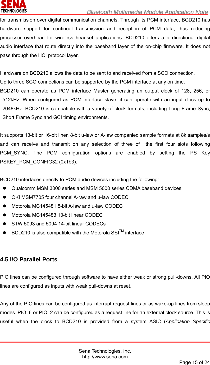
![BBlluueettooootthh MMuullttiimmeeddiiaa MMoodduullee AApppplliiccaattiioonn NNoottee Sena Technologies, Inc. http://www.sena.com Page 14 of 24 As USB is a Master/Slave oriented system (in common with other USB peripherals), BCD210 only supports USB slave operation. The USB data lines emerge as pins USB_DP and USB_DN. These terminals are connected to the internal USB I/O buffers of the BCD210, therefore, have low output impedance. To match the connection to the characteristic of the USB cable, resistors must be placed in series with USB_DP/USB_DN and the cable. BCD210 features an internal USB pull-up resistor. This pulls the USB_DP pin weakly high when BCD210 is ready to enumerate. It signals to the PC that it is a full speed (12Mbit/s) USB device. The USB internal pull-up is implemented as a current source, and is compliant with section 7.1.5 of the USB specification v1.2. The internal pull-up pulls USB_DP high to at least 2.8V when loaded with a 15KΩ±5% pull-down resistor (in the hub/host) when VDD_PADS=3.1V. This presents a Thevenin resistance to the host of at least 900Ω. Alternatively, an external 1.5KΩ pull-up resistor can be placed between a PIO line and D+ on the USB cable. The firmware must be alerted to which mode is used by PS key PSKEY_USB_PIO_PULLUP appropriately. The default setting uses the internal pull-up resistor. 4.3 I2C Interface PIO[8:6] can be used to form a mater I2C interface. The interface is formed using software to drive these lines. Therefore, it is suited only to relatively slow functions such as driving a dot matrix LCD (Liquid Crystal Display), keyboard scanner or EEPROM. Notes: PIO lines need to be pull-up through 2.2KΩ resistors. PIO[7:6] dual functions, UART bypass and EEPROM support, therefore, devices using an EEPROM cannot support UART bypass mode. For connection to EEPROMs, refer to CSR documentation on I2C EEPROM for use with BlueCore. This provides information on the type of devices currently supported. 4.4 PCM CODEC Interface PCM (Pulse Code Modulation) is a standard method used to digitize audio (particularly voice)](https://usermanual.wiki/SENA-TECHNOLOGIES/IW03/User-Guide-1695758-Page-14.png)

![BBlluueettooootthh MMuullttiimmeeddiiaa MMoodduullee AApppplliiccaattiioonn NNoottee Sena Technologies, Inc. http://www.sena.com Page 17 of 24 5. Application Schematic [Power Supply and Reset Interface] [Serial Interface for Host PC]](https://usermanual.wiki/SENA-TECHNOLOGIES/IW03/User-Guide-1695758-Page-17.png)
![BBlluueettooootthh MMuullttiimmeeddiiaa MMoodduullee AApppplliiccaattiioonn NNoottee Sena Technologies, Inc. http://www.sena.com Page 18 of 24 [USB Interface] [I2C Interface] [PCM Interface]](https://usermanual.wiki/SENA-TECHNOLOGIES/IW03/User-Guide-1695758-Page-18.png)
![BBlluueettooootthh MMuullttiimmeeddiiaa MMoodduullee AApppplliiccaattiioonn NNoottee Sena Technologies, Inc. http://www.sena.com Page 19 of 24 7. Solder Profiles The soldering profile depends on various parameters necessitating a set up for each application. The data here is given only for guidance on solder re-flow. There are four zones: Preheat Zone – This zone raises the temperature at a controlled rate, typically 1-2.5°C/s Equilibrium Zone – This zone brings the board to a uniform temperature and also activates the flux. The duration in this zone (typically 2-3 minutes) will need to be adjusted to optimize the out gassing of the flux. Reflow Zone – The peak temperature should be high enough to achieve good wetting but not so high as to cause component discoloration or damage. Excessive soldering time can lead to intermetal growth which can result in a brittle joint. Cooling Zone – The cooling rate should be fast, to keep the solder grains small which will give a longer lasting joint. Typical rates will be 2-5°C/s [Typical Lead-Free Re-flow Solder Profile] Key features of the profile: Initial Ramp = 1-2.5°C/sec to 175°C±25°C equilibrium Equilibrium time = 60 to 180 seconds Ramp to Maximum temperature (245°C) = 3°C/sec max. Time above liquids temperature (217°C): 45~90 seconds Device absolute maximum reflow temperature: 260°C Devices will withstand the specified profile. Lead-free devices will withstand up to three reflows to a maximum temperature of 260°C](https://usermanual.wiki/SENA-TECHNOLOGIES/IW03/User-Guide-1695758-Page-19.png)