SENA TECHNOLOGIES IW03 BLUETOOTH MODULE User Manual
Sena Technologies,Inc. BLUETOOTH MODULE Users Manual
Users Manual

B
Bl
lu
ue
et
to
oo
ot
th
h
M
Mu
ul
lt
ti
im
me
ed
di
ia
a
M
Mo
od
du
ul
le
e
A
Ap
pp
pl
li
ic
ca
at
ti
io
on
n
N
No
ot
te
e
Sena Technologies, Inc.
http://www.sena.com
Page 1 of 24
Bluetooth® Serial Module
Application Note
Bluetooth Class 2 OEM Module
Model: Parani-BCD210
Ver 1.0

B
Bl
lu
ue
et
to
oo
ot
th
h
M
Mu
ul
lt
ti
im
me
ed
di
ia
a
M
Mo
od
du
ul
le
e
A
Ap
pp
pl
li
ic
ca
at
ti
io
on
n
N
No
ot
te
e
Sena Technologies, Inc.
http://www.sena.com
Page 2 of 24
1. General
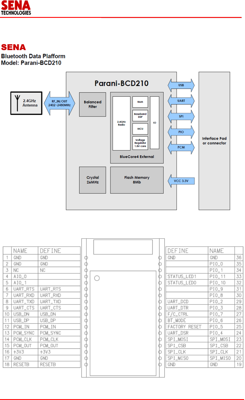
The Parani-BCD210 is a Bluetooth Class 2 OEM module for OEM manufacturers who want to
implement Bluetooth Class 2 functionality with their products cost effectively and also in timely
manner. Users can build their own antenna circuit around the BCD210 to lower the overall cost
while benefit from the BCD210’s field-proven standard SPP (Serial Port Profile) firmware
provided with no additional cost.
The BCD210 supports Class 1 Bluetooth transmission level for longer communication distance
typically ranges from 100 m up to 1 km. The BCD210 supports UART, USB, I2C, PCM, PIO
interfaces for the communication with the OEM products.
The BCD210 is provided with Bluetooth v2.0 compatible firmware runs internally for SPP (Serial
Port Profile) applications by default. The SPP firmware supports up to 4 simultaneous multiple
connections and is designed to work out-of-box for real world SPP applications such as POS
(Point-of-sales), industrial automation, remote metering and other various applications.
Optionally, the BCD210 can be supplied with only software stack up to HCI level so entire
Bluetooth stack runs on the host side for the application such as USB dongles for computers, or
OEM manufacturers can even develop and embed their own firmware into the BCD210.
The BCD210 is fully qualified with Bluetooth v.2.0+EDR specification so OEM manufacturers
can save cost and time for overall OEM product certifications, which makes the BCD210 ideal
solution for larger volume and cost sensitive applications.
To comply with FCC RF exposure compliance requirements, the antenna used for this
transmitter must be installed to provide a separation distance of at least 20 cm from all persons
and must not be co-located or operate in conjunction with any other antenna or transmitter.”
As such, the radio component of this device is intended only for OEM integrators under the
following two conditions: The antenna must be installed such that 20 cm is maintained between
the antenna and users.
The transmitter module may not be co-located with any other transmitter or antenna.
As long as the two conditions above are met, further transmitter testing will not be required.
However, the OEM integrator is still responsible for testing their end product for any additional
compliance requirements required with this module installed (e.g., digital device emissions, PC
peripheral requirements).
In the event that these conditions cannot be met (for example, co-location with another
transmitter), then the FCC authorization is no longer considered valid and the FCC ID cannot be
used on the final product. In these circumstances, the OEM integrator will be responsible for re-
evaluating the end product (including the transmitter) and obtaining a separate FCC

B
Bl
lu
ue
et
to
oo
ot
th
h
M
Mu
ul
lt
ti
im
me
ed
di
ia
a
M
Mo
od
du
ul
le
e
A
Ap
pp
pl
li
ic
ca
at
ti
io
on
n
N
No
ot
te
e
Sena Technologies, Inc.
http://www.sena.com
Page 3 of 24
authorization.
End Product Labeling
The final end product must be labeled in a visible area with the following :
“Contains Transmitter Module FCC ID: S7AIW03”.
The radio component is an integral part of the Parani-BCD210DU and cannot be removed.
1.1 Features
■ Fully qualified Bluetooth v2.0 + EDR
■ Full-speed Bluetooth operation
■ Full piconet and scatternet support
■ Minimum external components
■ Low-power 1.8V operation
■ 1.8V core, 1.8 to 3.6V I/O
■ Integrated 1.8V regulator
■ 8 x 8mm, 96-ball TFBGA and 6 x 6mm, 96-ball, VFBGA package options
■ USB v2.0 and dual UART ports
■ Support for IEEE 802.11 coexistence
■ Support for 8Mbit external Flash
■ Green (RoHS and no antimony or halogenated flame retardants)
1.2 Applications
■ PCs
■ PDAs
■ Computer accessories (compact Flash cards, PCMCIA cards, SD cards and USB dongles)
■ Access points
■ Digital cameras

B
Bl
lu
ue
et
to
oo
ot
th
h
M
Mu
ul
lt
ti
im
me
ed
di
ia
a
M
Mo
od
du
ul
le
e
A
Ap
pp
pl
li
ic
ca
at
ti
io
on
n
N
No
ot
te
e
Sena Technologies, Inc.
http://www.sena.com
Page 4 of 24
Model despription
Model name Interface Connector Antenna
Type1 Type2 Type3
Parani-BCD210DU DIP, pin U.FL 5dBi dipole 3dBi dipole 1dBi stub
Parani-BCD210DS DIP, pin RPSMA 5dBi dipole 3dBi dipole 1dBi stub
Parani-BCD210DC DIP, pin CHIP 0dBi Chip
Parani-BCD210SU SMD, pad U.FL 5dBi dipole 3dBi dipole 1dBi stub
Parani-BCD210SC SMD, pad CHIP 0dBi Chip
Use Antenna
Dipole antenna (M/N: R-AN2400-1901RS) Max Gain 5.37 dBi
Dipole antenna (M/N: R-AN2400-5801RS) Max Gain 3.27 dBi
Dipole antenna (M/N: AN2400-3306RS) Max Gain 1.40 dBi
Chip antenna (SENA_F0615) Max Gain: 0.2dBi
B
Bl
lu
ue
et
to
oo
ot
th
h
M
Mu
ul
lt
ti
im
me
ed
di
ia
a
M
Mo
od
du
ul
le
e
A
Ap
pp
pl
li
ic
ca
at
ti
io
on
n
N
No
ot
te
e
Sena Technologies, Inc.
http://www.sena.com
Page 5 of 24
1.3 Device Diagram
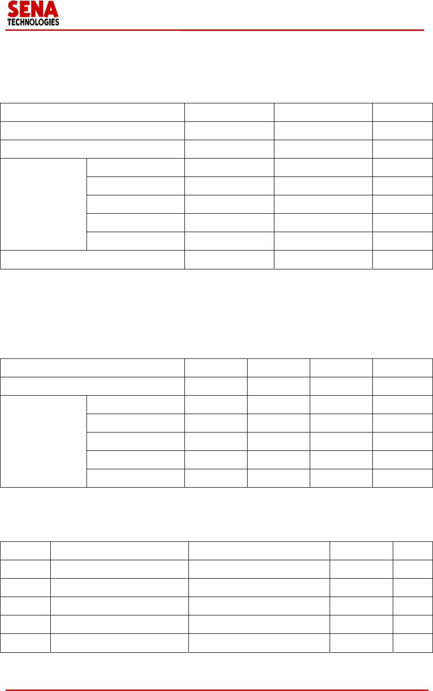
1.4 Pin Diagram

B
Bl
lu
ue
et
to
oo
ot
th
h
M
Mu
ul
lt
ti
im
me
ed
di
ia
a
M
Mo
od
du
ul
le
e
A
Ap
pp
pl
li
ic
ca
at
ti
io
on
n
N
No
ot
te
e
Sena Technologies, Inc.
http://www.sena.com
Page 6 of 24
1.5 Pin Descriptions
Function Pin Name Pin Number Description
USB Interface USB_DP 8 USB data plus
USB_DN 7 USB data minus
UART Interface UART_TXD 11 UART data output
UART_RXD 12 UART data input
UART_RTS 10 UART request to send active low
UART_CTS 9 UART clear to send active low
PCM Interface PCM_OUT 25 Synchronous data output
PCM_IN 24 Synchronous data input
PCM_SYNC 23 Synchronous data sync
PCM_CLK 22 Synchronous data clock
SPI Interface SPI_MISO 30 SPI data output
SPI_MOSI 32 SPI data input
SPI_CSB 29 Chip select for SPI, active low
SPI_CLK 31 SPI clock
PIO Interface
PIO_0 50 Programmable input/output line
PIO_1 49 Programmable input/output line
PIO_2 52 Programmable input/output line
PIO_3 51 Programmable input/output line
PIO_4 1 Programmable input/output line
PIO_5 20 Programmable input/output line
PIO_6 4 Programmable input/output line
PIO_7 3 Programmable input/output line
PIO_8 19 Programmable input/output line
PIO_9 13 Programmable input/output line
PIO_10 6 Programmable input/output line
PIO_11 14 Programmable input/output line
PIO_12 2 Programmable input/output line
PIO_13 15 Programmable input/output line
PIO_14 5 Programmable input/output line
PIO_15 21 Programmable input/output line
AIO_0 54 Analogue programmable input/output line

B
Bl
lu
ue
et
to
oo
ot
th
h
M
Mu
ul
lt
ti
im
me
ed
di
ia
a
M
Mo
od
du
ul
le
e
A
Ap
pp
pl
li
ic
ca
at
ti
io
on
n
N
No
ot
te
e
Sena Technologies, Inc.
http://www.sena.com
Page 7 of 24
AIO_1 55 Analogue programmable input/output line
Power VCC 16 Power supply for system, I/O, 3.3V
VCHG 35 Lithium ion/polymer battery charger input
VBAT 34 Lithium ion/polymer battery positive terminal
VREG_EN 33 Take high to enable internal regulators
GND 17 Ground
GND 18 Ground
GND 28 Ground
GND 36 Ground
GND 46 Ground
GND 48 Ground
GND 56 Ground
LED Drivers LED_0 26 LED driver
LED_1 27 LED driver
Others RF_I/O 47 Transmitter output/receiver input
RESETB 53 Reset, active low, > 5ms to cause a reset
B
Bl
lu
ue
et
to
oo
ot
th
h
M
Mu
ul
lt
ti
im
me
ed
di
ia
a
M
Mo
od
du
ul
le
e
A
Ap
pp
pl
li
ic
ca
at
ti
io
on
n
N
No
ot
te
e
Sena Technologies, Inc.
http://www.sena.com
Page 8 of 24
2. Electrical characteristics
2.1 Absolute maximum ratings
Ratings Min Max Unit
Storage Temperature -40 +85 °C
Operating Temperature -40 +85 °C
Supply voltage VCC -0.4 3.6 V
VREG_EN -0.4 4.9 V
VBAT -0.4 4.4 V
LED[1:0] -0.4 4.4 V
VCHG -0.4 6.5 V
Other terminal voltages GND – 0.4 VCC + 0.4 V
2.2 Recommended operating conditions
Ratings Min Typ Max Unit
Operating Temperature -30 20 +70 °C
Supply voltage VCC 3.1 3.3 3.5 V
VREG_EN 2.8 4.2 4.4 V
VBAT 2.8 4.2 4.4 V
LED[1:0] 2.8 4.2 4.4 V
VCHG 4.5 5.0 5.5 V
2.3 Power Consumption

B
Bl
lu
ue
et
to
oo
ot
th
h
M
Mu
ul
lt
ti
im
me
ed
di
ia
a
M
Mo
od
du
ul
le
e
A
Ap
pp
pl
li
ic
ca
at
ti
io
on
n
N
No
ot
te
e
Sena Technologies, Inc.
http://www.sena.com
Page 9 of 24
3. RF Characteristics
3.1 Basic Data Rate
3.1.1 Transmitter Performance
RF Characteristics
VCC = 3.3V, 20°C
Min Typ Max Bluetooth
Specification
Unit
Output power 2 4 6 20 dBm
Power Density 2 4 6 20 dBm
Power Control 2 4 6 2 ≤ step ≤ 8 dB
TX Output Spectrum-Frequency range - - - 2400 ~2483.5 MHz
TX Output Spectrum-20dB Bandwidth - 940 1000 ≤ 1000 kHz
Adjacent
Channel Power
F = F0 ± 2MHz - -36 -20 ≤ -20 dBm
F = F0 ± 3MHz - -45 -40 ≤ -40 dBm
F = F0 ± > 3MHz - -50 -40 ≤ -40 dBm
Modulation
Characteristics
∆f1avg 140 165 175 140 ≤ ∆f1avg ≤ 175 kHz
∆f2avg 115 142 - ∆f2avg ≥ 115 kHz
∆f2avg/∆f1avg 0.80 0.92 - (∆f1avg/∆f2avg) ≥ 0.8
Initial Carrier Frequency Tolerance -75 ±20 75 ≤ ±75 kHz
Carrier
Frequency Drift
Drift rate -20 - 20 ≤ ±20 kHz/50µs
1 slot Freq Drift -25 - 25 ≤ ±25 kHz
5 slot Freq Drift -40 - 40 ≤ ±40 kHz
B
Bl
lu
ue
et
to
oo
ot
th
h
M
Mu
ul
lt
ti
im
me
ed
di
ia
a
M
Mo
od
du
ul
le
e
A
Ap
pp
pl
li
ic
ca
at
ti
io
on
n
N
No
ot
te
e
Sena Technologies, Inc.
http://www.sena.com
Page 10 of 24
3.1.2 Transceiver
RF Characteristics
VCC = 3.3V, 20°C
Min Typ Max Specification Unit
Out of band
Spurious
Emissions
0.030-1.000GHz - - -36 ≤ -36 dBm
1.000-12.75GHz - - -30 ≤ -30 dBm
1.800-5.100GHz - - -47 ≤ -47 dBm
5.100-5.300GHz - - -47 ≤ -47 dBm
3.1.3 Receiver Performance
RF Characteristics
VCC = 3.3V, 20°C
Min Typ Max Bluetooth
Specification
Unit
Sensitivity - Single slot packets (0.1%) -88 -85 -82 ≤ -70 dBm
Sensitivity - Multi slot packets (0.1%) -88 -85 -82 ≤ -70 dBm
C/I performance
at 0.1% BER
co-channel - - 11 ≤ -11 dB
F = F0 + 1MHz - - 0 ≤ 0 kHz
F = F0 – 1MHz - - 0 ≤ 0 dB
F = F0 + 2MHz - - -20 ≤ -20 dB
F = F0 – 2MHz - - -30 ≤ -30 dB
F = F0 – 3MHz - - -40 ≤ -40 dB
F = F0 + 5MHz - - -40 ≤ -40 dB
F = FImage - - -9 ≤ -9 dB
Blocking
performance
0.030-2.000GHz -10 - - -10 dBm
2.000-2.400GHz -27 - - -27 dBm
2.500-3.000GHz -27 - - -27 dBm
3.000-12.75GHz -10 - - -10 dBm
Inter-modulation performance -39 - - ≥ -39 dBm
Maximum input level at 0.1% BER -20 - - ≥ -20 dBm

B
Bl
lu
ue
et
to
oo
ot
th
h
M
Mu
ul
lt
ti
im
me
ed
di
ia
a
M
Mo
od
du
ul
le
e
A
Ap
pp
pl
li
ic
ca
at
ti
io
on
n
N
No
ot
te
e
Sena Technologies, Inc.
http://www.sena.com
Page 11 of 24
3.2 Enhanced Data Rate
3.2.1 Transmitter performance
RF Characteristics
VCC = 3.3V, 20°C
Min Typ Max Bluetooth
Specification
Unit
Maximum RF Transmit Power 0 2 4 -6 to +4 dB
Relative Transmit Power -4 -1 1 -4 to +1 dB
Carrier
Frequency
Stability
π/4
DQPSK
| ω0 | -10 - 10 ≤ ±10 for all blocks kHz
| ωi | -75 - 75 ≤ ±75 for all packets kHz
| ω0 + ωi | -75 - 75
≤ ±75 for all blocks kHz
8DPSK | ω0 | -10 - 10 ≤ ±10 for all blocks kHz
| ωi | -75 - 75 ≤ ±75 for all packets kHz
| ω0 + ωi | -75 - 75
≤ ±75 for all blocks kHz
Modulation
Accuracy
π/4
DQPSK
RMS DEVM - - 20 ≤ 20 %
99% DEVM - - 30 ≤ 30 %
Peak DEVM - - 35 ≤ 35 %
8DPSK RMS DEVM - - 13 ≤ 13 %
99% DEVM - - 20 ≤ 20 %
Peak DEVM - - 25 ≤ 25 %
EDR Differential Phase Encoding 99 - - ≥ 99 %
In-band
Spurious
Emissions
(8DPSK)
F ≥ F0 + 3MHz - - -40 ≥ -40 dBm
F < F0 + 3MHz - - -40 ≥ -40 dBm
F = F0 – 3MHz - - -40 ≥ -40 dBm
F = F0 – 2MHz - - -20 ≥ -20 dBm
F = F0 – 1MHz - - -26 ≥ -26 dB
F = F0 + 1MHz - - -26 ≥ -26 dB
F = F0 + 2MHz - - -20 ≥ -20 dBm
F = F0 + 3MHz - - -40 ≥ -40 dBm

B
Bl
lu
ue
et
to
oo
ot
th
h
M
Mu
ul
lt
ti
im
me
ed
di
ia
a
M
Mo
od
du
ul
le
e
A
Ap
pp
pl
li
ic
ca
at
ti
io
on
n
N
No
ot
te
e
Sena Technologies, Inc.
http://www.sena.com
Page 12 of 24
3.2.2 Receiver performance
RF Characteristics
VCC = 3.3V, 25°C
Min Typ Max Bluetooth
Specification
Unit
Sensitivity
at 0.01% BER
π/4 DQPSK -87 -84 -81 ≤ -70 dBm
8DPSK -87 -84 -81 ≤ -70 dBm
BER floor performance - - -60 ≤ -60 dBm
C/I Performance
(co-channel at 0.1% BER)
π/4 DQPSK - - 13 ≤ +13 dB
8DPSK - - 21 ≤ +21 dB
C/I
Performance
(Adjacent
Channel
Selectivity)
F = F0 + 1MHz π/4 DQPSK - - 0 ≤ 0 dB
8DPSK - - 5 ≤ +5 dB
F = F0 – 1MHz π/4 DQPSK - - 0 ≤ 0 dB
8DPSK - - 5 ≤ +5 dB
F = F0 + 2MHz π/4 DQPSK - - -30 ≤ -30 dB
8DPSK - - -25 ≤ -25 dB
F = F0 – 2MHz π/4 DQPSK - - -20 ≤ -20 dB
8DPSK - - -13 ≤ -13 dB
F ≥ F0 + 3MHz π/4 DQPSK - - -40 ≤ -40 dB
8DPSK - - -33 ≤ -33 dB
F ≤ F0 – 5MHz π/4 DQPSK - - -40 ≤ -40 dB
8DPSK - - -33 ≤ -33 dB
F = FImage π/4 DQPSK - - -7 ≤ -7 dB
8DPSK - - 0 ≤ 0 dB
Maximum input level
at 0.1% BER
π/4 DQPSK -20 - - ≥ -20 dBm
8DPSK -20 - - ≥ -20 dBm
B
Bl
lu
ue
et
to
oo
ot
th
h
M
Mu
ul
lt
ti
im
me
ed
di
ia
a
M
Mo
od
du
ul
le
e
A
Ap
pp
pl
li
ic
ca
at
ti
io
on
n
N
No
ot
te
e
Sena Technologies, Inc.
http://www.sena.com
Page 13 of 24
4. Device Terminal Descriptions
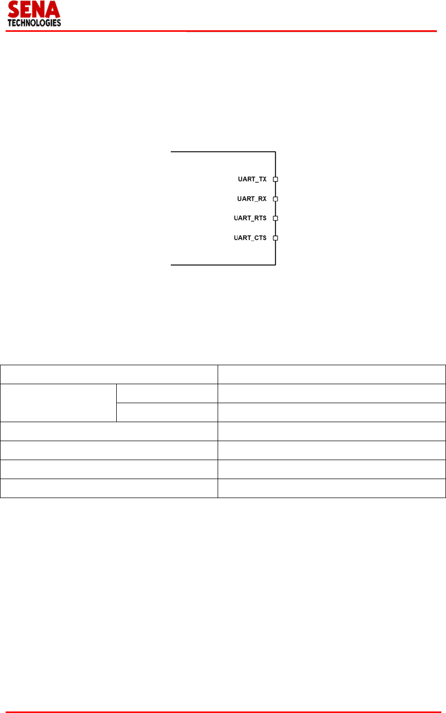
4.1 UART Interface
This is a standard UART interface for communicating with other serial devices.
BCD210 UART interface provides a simple mechanism for communicating with other serial
device using the RS232 protocol.
When BCD210 is connected to another digital device, UART_RX and UART_TX transfer data
between the two devices. The remaining two signals, UART_CTS, UART_RTS, can be used to
implement RS232 hardware flow control where both are active low indicators. All UART
connections are implemented using CMOS technology and have signaling levels of 0V and 3.3V
Parameter Possible Values
Baud Rate Minimum 1200 baud (2%Error)
Maximum 4M baud (1%Error)
Flow Control RTS/CTS or None
Parity None, Odd or Even
Number of Stop Bits 1 or 2
Bits per Channel 8
[Possible UART Settings]
4.2 USB Interface
BCD210 USB devices contain a full speed (12Mbits/s) USB interface that is capable of driving
of a USB cable directly. No external USB transceiver is required. The device operates as a USB
peripheral, responding to requests from a master host controller such as a PC. Both the OHCI
and the UHCI standards are supported. The set of USB endpoints implemented behave as
specified in the USB section of the Bluetooth specification v2.0+EDR or alternatively can appear
as a set of endpoints appropriate to USB audio devices such as speakers.

B
Bl
lu
ue
et
to
oo
ot
th
h
M
Mu
ul
lt
ti
im
me
ed
di
ia
a
M
Mo
od
du
ul
le
e
A
Ap
pp
pl
li
ic
ca
at
ti
io
on
n
N
No
ot
te
e
Sena Technologies, Inc.
http://www.sena.com
Page 14 of 24
As USB is a Master/Slave oriented system (in common with other USB peripherals), BCD210
only supports USB slave operation.
The USB data lines emerge as pins USB_DP and USB_DN. These terminals are connected to
the internal USB I/O buffers of the BCD210, therefore, have low output impedance. To match
the connection to the characteristic of the USB cable, resistors must be placed in series with
USB_DP/USB_DN and the cable.
BCD210 features an internal USB pull-up resistor. This pulls the USB_DP pin weakly high when
BCD210 is ready to enumerate. It signals to the PC that it is a full speed (12Mbit/s) USB device.
The USB internal pull-up is implemented as a current source, and is compliant with section
7.1.5 of the USB specification v1.2. The internal pull-up pulls USB_DP high to at least 2.8V
when loaded with a 15KΩ±5% pull-down resistor (in the hub/host) when VDD_PADS=3.1V. This
presents a Thevenin resistance to the host of at least 900Ω. Alternatively, an external 1.5KΩ
pull-up resistor can be placed between a PIO line and D+ on the USB cable. The firmware must
be alerted to which mode is used by PS key PSKEY_USB_PIO_PULLUP appropriately. The
default setting uses the internal pull-up resistor.
4.3 I2C Interface
PIO[8:6] can be used to form a mater I2C interface. The interface is formed using software to
drive these lines. Therefore, it is suited only to relatively slow functions such as driving a dot
matrix LCD (Liquid Crystal Display), keyboard scanner or EEPROM.
Notes:
PIO lines need to be pull-up through 2.2KΩ resistors.
PIO[7:6] dual functions, UART bypass and EEPROM support, therefore, devices using an
EEPROM cannot support UART bypass mode.
For connection to EEPROMs, refer to CSR documentation on I2C EEPROM for use with
BlueCore. This provides information on the type of devices currently supported.
4.4 PCM CODEC Interface
PCM (Pulse Code Modulation) is a standard method used to digitize audio (particularly voice)

B
Bl
lu
ue
et
to
oo
ot
th
h
M
Mu
ul
lt
ti
im
me
ed
di
ia
a
M
Mo
od
du
ul
le
e
A
Ap
pp
pl
li
ic
ca
at
ti
io
on
n
N
No
ot
te
e
Sena Technologies, Inc.
http://www.sena.com
Page 15 of 24
for transmission over digital communication channels. Through its PCM interface, BCD210 has
hardware support for continual transmission and reception of PCM data, thus reducing
processor overhead for wireless headset applications. BCD210 offers a bi-directional digital
audio interface that route directly into the baseband layer of the on-chip firmware. It does not
pass through the HCI protocol layer.
Hardware on BCD210 allows the data to be sent to and received from a SCO connection.
Up to three SCO connections can be supported by the PCM interface at any on time.
BCD210 can operate as PCM interface Master generating an output clock of 128, 256, or
512kHz. When configured as PCM interface slave, it can operate with an input clock up to
2048kHz. BCD210 is compatible with a variety of clock formats, including Long Frame Sync,
Short Frame Sync and GCI timing environments.
It supports 13-bit or 16-bit liner, 8-bit u-law or A-law companied sample formats at 8k samples/s
and can receive and transmit on any selection of three of the first four slots following
PCM_SYNC. The PCM configuration options are enabled by setting the PS Key
PSKEY_PCM_CONFIG32 (0x1b3).
BCD210 interfaces directly to PCM audio devices including the following:
Qualcomm MSM 3000 series and MSM 5000 series CDMA baseband devices
OKI MSM7705 four channel A-raw and u-law CODEC
Motorola MC145481 8-bit A-law and u-law CODEC
Motorola MC145483 13-bit linear CODEC
STW 5093 and 5094 14-bit linear CODECs
BCD210 is also compatible with the Motorola SSITM interface
4.5 I/O Parallel Ports
PIO lines can be configured through software to have either weak or strong pull-downs. All PIO
lines are configured as inputs with weak pull-downs at reset.
Any of the PIO lines can be configured as interrupt request lines or as wake-up lines from sleep
modes. PIO_6 or PIO_2 can be configured as a request line for an external clock source. This is
useful when the clock to BCD210 is provided from a system ASIC (Application Specific

B
Bl
lu
ue
et
to
oo
ot
th
h
M
Mu
ul
lt
ti
im
me
ed
di
ia
a
M
Mo
od
du
ul
le
e
A
Ap
pp
pl
li
ic
ca
at
ti
io
on
n
N
No
ot
te
e
Sena Technologies, Inc.
http://www.sena.com
Page 16 of 24
Integrated Circuit). Using PSKEY_CLOCK_REQUEST_ENABLE (0x246), this terminal can be
configured to be low when BCD210 is in Deep Sleep and high when a clock is required. The
clock must be supplied within 4ms of the rising edge of PIO_6 or PIO_2 to avoid losing timing
accuracy in certain Bluetooth operating modes.
BCD210 has three general purpose analogue interface pins, AIO_0, AIO_1 and AIO_2. These
are used to access internal circuitry and control signals. One pin is allocated to decoupling for
the on-chip band gap reference voltage, the other two may be configured to provide additional
functionality.
4.6 Reset Interface
BCD210 may be reset from several sources: RESETB pin, power on reset, a UART break
character or via a software configured watchdog timer.
The RESETB pin is an active low reset and is internally filtered using the internal low frequency
clock oscillator. A reset will be performed between 1.5 and 4.0ms following RESETB being
active. It is recommended that RESETB be applied for a period greater than 5ms.
The power on reset occurs when the VDD_CORE supply falls below typically 1.5V and is
released when VDD_CORE rises above typically 1.6V.
At reset the digital I/O pins are set to inputs for bi-directional pins and outputs are tri-state. The
PIOs have weak pull-downs.
B
Bl
lu
ue
et
to
oo
ot
th
h
M
Mu
ul
lt
ti
im
me
ed
di
ia
a
M
Mo
od
du
ul
le
e
A
Ap
pp
pl
li
ic
ca
at
ti
io
on
n
N
No
ot
te
e
Sena Technologies, Inc.
http://www.sena.com
Page 17 of 24
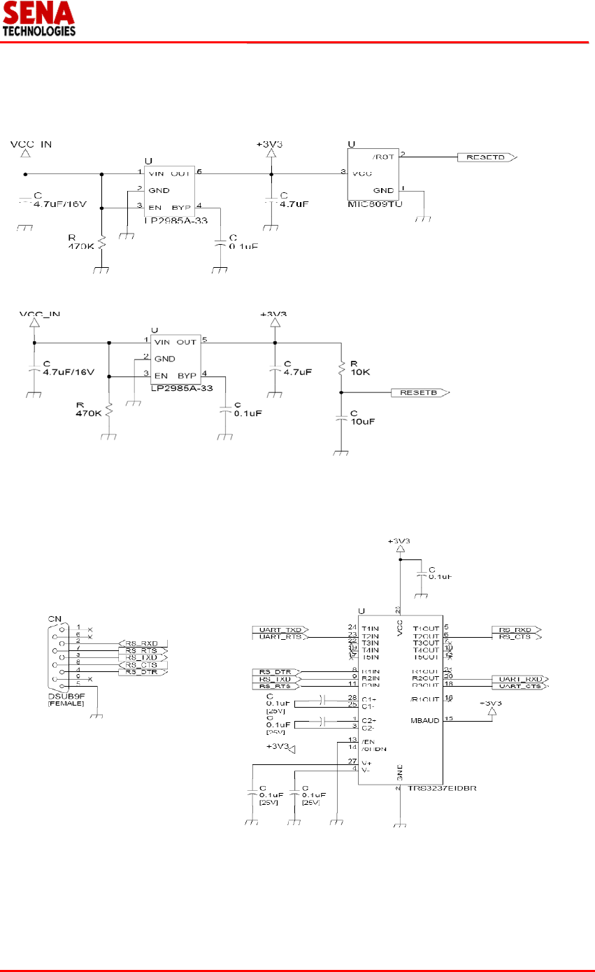
5. Application Schematic
[Power Supply and Reset Interface]
[Serial Interface for Host PC]
B
Bl
lu
ue
et
to
oo
ot
th
h
M
Mu
ul
lt
ti
im
me
ed
di
ia
a
M
Mo
od
du
ul
le
e
A
Ap
pp
pl
li
ic
ca
at
ti
io
on
n
N
No
ot
te
e
Sena Technologies, Inc.
http://www.sena.com
Page 18 of 24
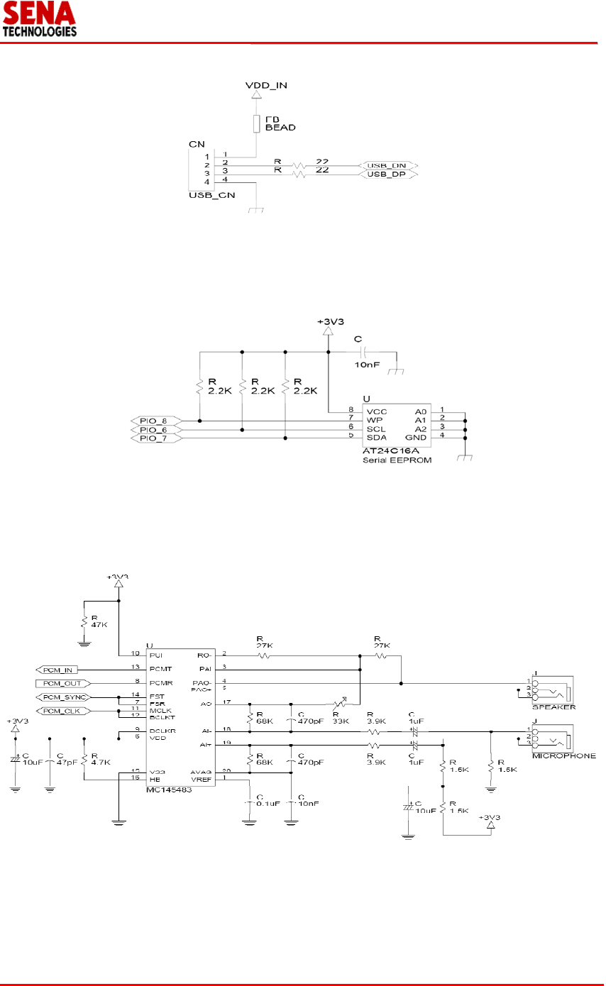
[USB Interface]
[I2C Interface]
[PCM Interface]
B
Bl
lu
ue
et
to
oo
ot
th
h
M
Mu
ul
lt
ti
im
me
ed
di
ia
a
M
Mo
od
du
ul
le
e
A
Ap
pp
pl
li
ic
ca
at
ti
io
on
n
N
No
ot
te
e
Sena Technologies, Inc.
http://www.sena.com
Page 19 of 24
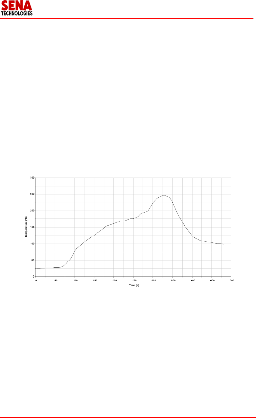
7. Solder Profiles
The soldering profile depends on various parameters necessitating a set up for each application.
The data here is given only for guidance on solder re-flow. There are four zones:
Preheat Zone – This zone raises the temperature at a controlled rate, typically 1-2.5°C/s
Equilibrium Zone – This zone brings the board to a uniform temperature and also
activates the flux. The duration in this zone (typically 2-3 minutes) will need to be adjusted
to optimize the out gassing of the flux.
Reflow Zone – The peak temperature should be high enough to achieve good wetting but
not so high as to cause component discoloration or damage. Excessive soldering time can
lead to intermetal growth which can result in a brittle joint.
Cooling Zone – The cooling rate should be fast, to keep the solder grains small which will
give a longer lasting joint. Typical rates will be 2-5°C/s
[Typical Lead-Free Re-flow Solder Profile]
Key features of the profile:
Initial Ramp = 1-2.5°C/sec to 175°C±25°C equilibrium
Equilibrium time = 60 to 180 seconds
Ramp to Maximum temperature (245°C) = 3°C/sec max.
Time above liquids temperature (217°C): 45~90 seconds
Device absolute maximum reflow temperature: 260°C
Devices will withstand the specified profile.
Lead-free devices will withstand up to three reflows to a maximum temperature of 260°C

B
Bl
lu
ue
et
to
oo
ot
th
h
M
Mu
ul
lt
ti
im
me
ed
di
ia
a
M
Mo
od
du
ul
le
e
A
Ap
pp
pl
li
ic
ca
at
ti
io
on
n
N
No
ot
te
e
Sena Technologies, Inc.
http://www.sena.com
Page 20 of 24
8. Packaging Information
TBD

B
Bl
lu
ue
et
to
oo
ot
th
h
M
Mu
ul
lt
ti
im
me
ed
di
ia
a
M
Mo
od
du
ul
le
e
A
Ap
pp
pl
li
ic
ca
at
ti
io
on
n
N
No
ot
te
e
Sena Technologies, Inc.
http://www.sena.com
Page 21 of 24
9. Contact Information
Technical Support
Sena Technologies, Inc.
210 Yangjae-dong, Seocho-gu
Seoul 137-130, Korea
Tel: (+82-2) 573-5422
Fax: (+82-2) 573-7710
E-Mail: support@sena.com
Website: http://www.sena.com
11. Document History
Date Revision Reason of Change

B
Bl
lu
ue
et
to
oo
ot
th
h
M
Mu
ul
lt
ti
im
me
ed
di
ia
a
M
Mo
od
du
ul
le
e
A
Ap
pp
pl
li
ic
ca
at
ti
io
on
n
N
No
ot
te
e
Sena Technologies, Inc.
http://www.sena.com
Page 22 of 24
12. Certificate Information
12.1 FCC
FCC Rule: Part 15 Subpart C Section 15.247
FCCID: S7AIW03
12.1.1 FCC Compliance Statement
This device complies with part 15 of the FCC Rules. Operation is subject to the following two
conditions:
(1) This device may not cause harmful interference, and
(2) This device must accept any interference received,
Including interference that may cause undesired operation
Information to User
This equipment has been tested and found to comply with limits for a Class B digital device,
Pursuant to Part 15 of the FCC Rules. These limits are designed to provide reasonable
protection against harmful interference in a residential installation.
This equipment generate, uses and can radiate radio frequency energy and, if not installed and
used in accordance with the instructions, may cause harmful interference to radio
communications.
However, there is no guarantee that interference will not occur in a particular installation. If this
equipment does cause harmful interference to radio or television reception, which can be
determined by turning the equipment off and on, the user is encouraged to try to correct the
interference by on or more of the following measures:
- Reorient or relocate the receiving antenna.
- Increase the separation between the equipment and receiver-Connect the equipment
into an outlet a circuit different form that to which the receiver is connected.
- Consult the dealer or an experienced radio/TV technician for help.
12.1.2 RF Exposure Statement
The equipment complies with FCC RF radiation exposure limits set forth for an uncontrolled
environment. This device and its antenna must not be co-located or operation in conjunction
with any other antenna or transmitter.
12.1.3 Do not
Any changes or modifications to the equipment not expressly approved by the party
responsible for compliance could void user’s authority to operate the equipment.
To comply with FCC RF exposure compliance requirements, the antenna used for this
transmitter must be installed to provide a separation distance of at least 20 cm from all persons
and must not be co-located or operate in conjunction with any other antenna or transmitter.”
As such, the radio component of this device is intended only for OEM integrators under the
following two conditions: The antenna must be installed such that 20 cm is maintained between
the antenna and users.
The transmitter module may not be co-located with any other transmitter or antenna.
As long as the two conditions above are met, further transmitter testing will not be required.
However, the OEM integrator is still responsible for testing their end product for any additional
compliance requirements required with this module installed (e.g., digital device emissions, PC
peripheral requirements).

B
Bl
lu
ue
et
to
oo
ot
th
h
M
Mu
ul
lt
ti
im
me
ed
di
ia
a
M
Mo
od
du
ul
le
e
A
Ap
pp
pl
li
ic
ca
at
ti
io
on
n
N
No
ot
te
e
Sena Technologies, Inc.
http://www.sena.com
Page 23 of 24
In the event that these conditions cannot be met (for example, co-location with another
transmitter), then the FCC authorization is no longer considered valid and the FCC ID cannot be
used on the final product. In these circumstances, the OEM integrator will be responsible for re-
evaluating the end product (including the transmitter) and obtaining a separate FCC
authorization.
End Product Labeling
The final end product must be labeled in a visible area with the following :
“Contains Transmitter Module FCC ID: S7AIW03”.
The radio component is an integral part of the Parani-BCD210DU and cannot be removed.
12.2 CE
1177
Declare under our own responsibility that the product
Bluetooth Module
Brand name: SENA
Model No.: Parani-BCD210DU / Parani-BCD210DC / Parani-BCD210DS
Parani-BCD210SU / Parani-BCD210SC
To which this declaration refers conforms with the relevant standards or other standardizing
documents
EN 60950-1
ETSI EN 301 489-1
ETSI EN 301 489-17
ETSI EN 300 328
According to the regulations in Directive 1999/5/EC
12.3 IC
“This device complies with Industry Canada licence-exempt RSS standard(s). Operation is
subject to the following two conditions: (1) this device may not cause interference, and (2) this
device must accept any interference, including interference that may cause undesired operation
of the device.”
Le présent appareil est conforme aux CNR d'Industrie Canada applicables aux appareils radio
exempts de licence. L'exploitation est autorisée aux deux conditions suivantes : (1) l'appareil ne
doit pas produire de brouillage, et (2) l'utilisateur de l'appareil doit accepter tout brouillage
radioélectrique subi, même si le brouillage est susceptible d'en compromettre le fonctionnement.
Radio Cert. No.: IC: 8154A-IW03
12.4 KC
Type Registration
Certification No: KCC-CRM-SNA-IW03

B
Bl
lu
ue
et
to
oo
ot
th
h
M
Mu
ul
lt
ti
im
me
ed
di
ia
a
M
Mo
od
du
ul
le
e
A
Ap
pp
pl
li
ic
ca
at
ti
io
on
n
N
No
ot
te
e
Sena Technologies, Inc.
http://www.sena.com
Page 24 of 24
12.5 JAPAN MIC
Technical Regulations for Specified Radio Equipment Article 2, Section 1 (19)
Certification No:
12.6 SIG
QDID: B016862
Model Name: Parani-BCD210
Core Version: 2.0+EDR
Product Type: End Product
Declared Specifications: Baseband Conformance, Radio, Service Discovery Protocol,
Logical Link Control and Adaption Protocol, Generic Access Profile, Link Manager,
RFCOMM,
Serial Port Profile, Host Controller Interface, Summary ICS, Product Type