SIMCom Wireless Solutions SIM7000A LTE CAT-M1(eMTC) and NB-IoT Module User Manual SIM7000A V1 00
Shanghai SIMCom Wireless Solutions Limited LTE CAT-M1(eMTC) and NB-IoT Module SIM7000A V1 00
Contents
- 1. TempConfidential_SIM7000A__User Manual_V1 00_20170728
- 2. SIM7000A__User Manual_V1 00
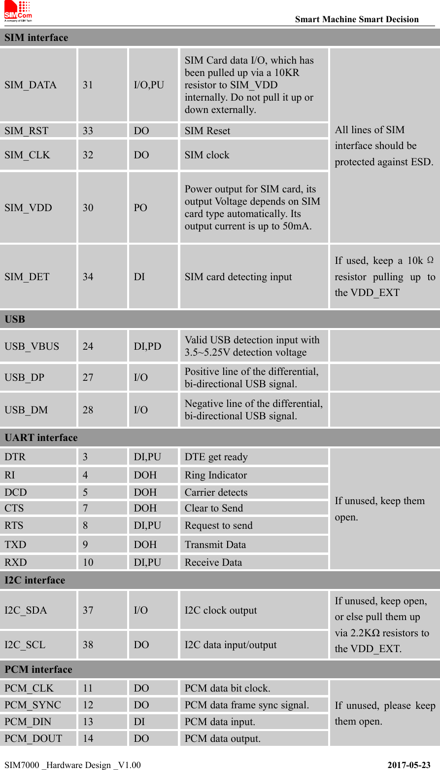
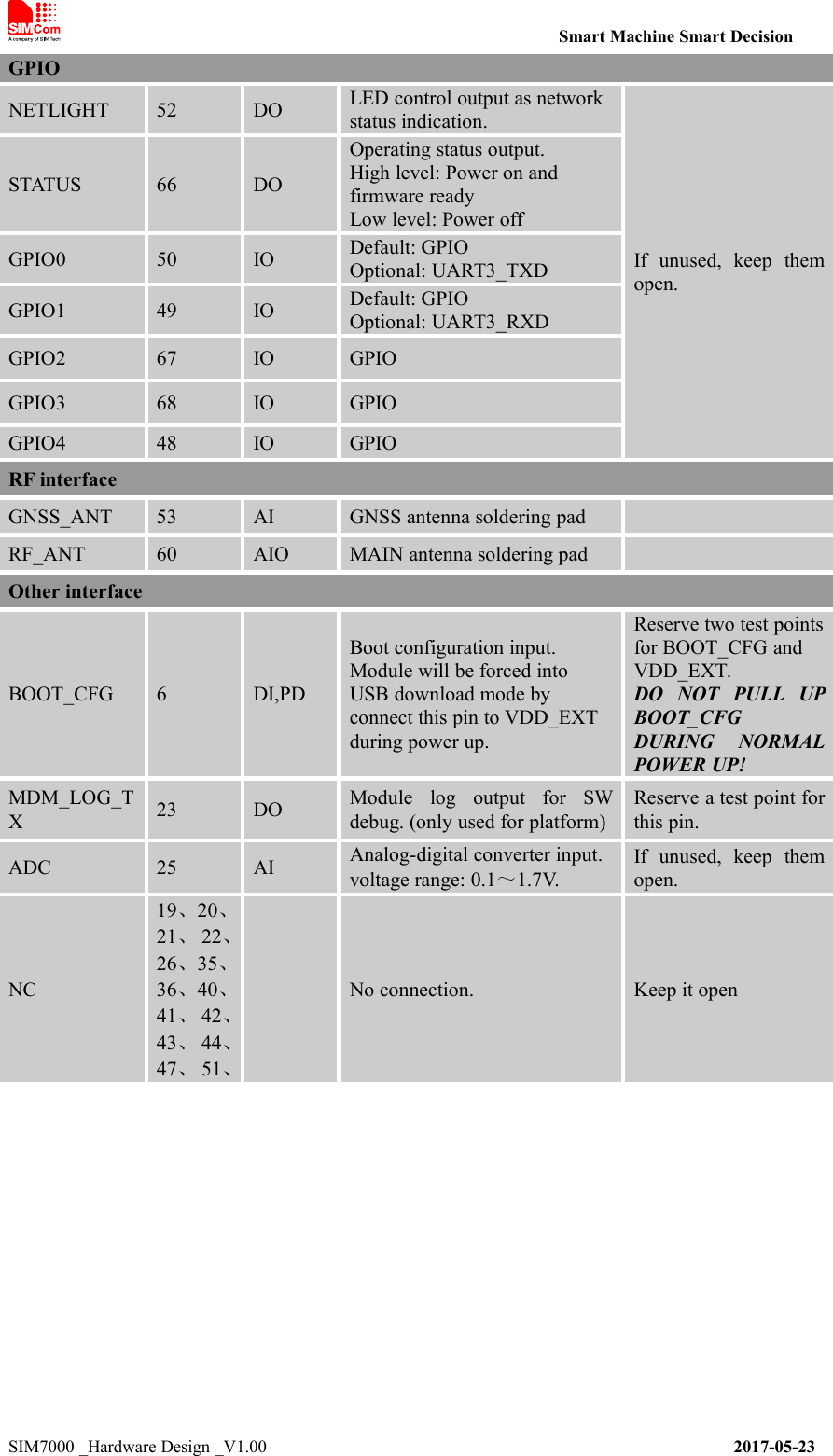
SIM7000A__User Manual_V1 00
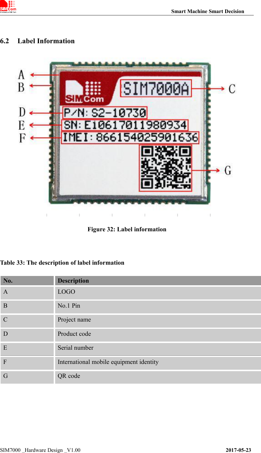
![Smart Machine Smart DecisionSIM7000 _Hardware Design _V1.00 2017-05-23The following figure shows the linear regulator reference circuit with 5V input and 3.8V output.Figure 7: Linear regulator reference circuitIf there is a big voltage difference between input and output for VBAT power supply, or theefficiency is extremely important, then a switching mode power supply will be preferable. Thefollowing figure shows the switching mode power supply reference circuit.Figure 8: Switching mode power supply reference circuitNote: The Switching Mode power supply solution for VBAT must be chosen carefully againstElectro Magnetic Interference and ripple current from depraving RF performance.3.1.3 Voltage MonitorTo monitor the VBAT voltage, the AT command “AT+CBC” can be used.To monitor whether the VBAT voltage is inside a special range, the AT command“AT+CBATCHK” can be used to enable the overvoltage warning function and the under-voltagewarning function. The default value of the overvoltage warning function in the software is 4.3V,and the default value of the under-voltage warning function is 3.1V.When the VBAT voltage is out of the range, the module will be power off. If users need to poweroff SIM7000 when the VBAT voltage is out of the range, the AT command “AT+CBATCHK” canbe used to enable the overvoltage power-off function and the under-voltage power-off function. Thedefault value of the overvoltage power-off function in the software is 4.4V, and the default value ofthe under-voltage power-off function is 2.9V.Note: Under-voltage warning function and under-voltage power-off function are disabled bydefault. For more information about these AT commands, please refer to Document [1].](https://usermanual.wiki/SIMCom-Wireless-Solutions/SIM7000A.SIM7000A-User-Manual-V1-00/User-Guide-4125651-Page-23.png)
![Smart Machine Smart DecisionSIM7000 _Hardware Design _V1.00 2017-05-23Table 8: Power on timing and electronic characteristicSymbolParameterMin.Typ.Max.UnitTonThe time of active low level impulse of PWRKEYpin to power on module72--msTon(status)The time from power-on issue to STATUS pinoutput high level(indicating power up ready )4.2--sTon(uart)The time from power-on issue to UART port ready3.5--sTon(usb)The time from power-on issue to USB port ready3.5--sVIHInput high level voltage on PWRKEY pin0.60.81.8VVILInput low level voltage on PWRKEY pin-0.300.5V3.2.2 Power offThe following methods can be used to power off SIM7000.●Method 1: Power off SIM7000 by pulling the PWRKEY pin to ground.●Method 2: Power off SIM7000 by AT command “AT+CPOWD”.●Method 3: over-voltage or under-voltage automatic power off. The voltage range can be set byAT command “AT+CBATCHK”.●Method 4: over-temperature or under-temperature automatic power off.Note: If the temperature is outside the range of -30~+80℃, some warning will be reported viaAT port. If the temperature is outside the range of -40~+85℃, SIM7000 will be powered offautomatically.For details about “AT+CPOWD” and “AT+CBATCHK”, please refer to Document [1].These procedures will make modules disconnect from the network and allow the software to enter asafe state, and save data before module be powered off completely.The power off scenario by pulling down the PWRKEY pin is illustrated in the following figure.Figure 11: Power off timing sequence](https://usermanual.wiki/SIMCom-Wireless-Solutions/SIM7000A.SIM7000A-User-Manual-V1-00/User-Guide-4125651-Page-25.png)
![Smart Machine Smart DecisionSIM7000 _Hardware Design _V1.00 2017-05-23Normally RI will be kept at a high level until a voice call, then it will output periodic rectangularwave with 5900ms low level and 100ms high level. It will output this kind of periodic rectangularwave until the call is answered or hung up.Figure 17: RI behaviour(voice call)Note: For more details of AT commands about UART, please refer to document [1] and [22].The DTR pin description:After setting the AT command “AT+CSCLK=1”, SIM7000 will enter sleep mode by pulling up theDTR pin when module is in the idle mode. In sleep mode, the UART is unavailable. WhenSIM7000 enters sleep mode, pulling down DTR can wake up module.3.4 USB InterfaceThe SIM7000 contains a USB interface compliant with the USB2.0 specification as a peripheral,but the USB charging function is not supported.SIM7000 supports the USB suspend and resume mechanism which can reduce power consumption.If there is no data transmission on the USB bus, SIM7000 will enter suspend mode automatically,and will be resumed by some events such as voice call, receiving SMS, etc.Figure 18: USB reference circuitBecause of the high speed on USB bus, more attention should be paid to the influence of thejunction capacitance of the ESD component on USB data lines. Typically, the capacitance of the D1and D2 should be less than 1pF.D3 is suggested to select the diode with anti-ESD and voltage surge function, or customer couldadd a ZENER diode for surge clamping.Note:The USB_DM and USB_DP nets must be traced by 90Ohm+/-10% differential impedance.](https://usermanual.wiki/SIMCom-Wireless-Solutions/SIM7000A.SIM7000A-User-Manual-V1-00/User-Guide-4125651-Page-29.png)
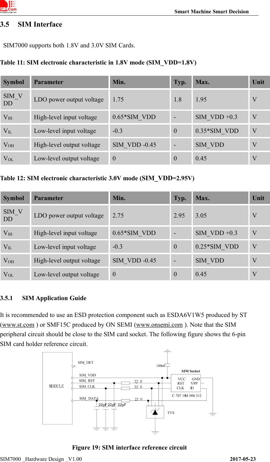
![Smart Machine Smart DecisionSIM7000 _Hardware Design _V1.00 2017-05-23Note: SIM_DATA has been pulled up with a 10KΩ resistor to SIM_VDD in module. A 100nFcapacitor on SIM_VDD is used to reduce interference. For more details of AT commands aboutSIM, please refer to document [1].SIM_CLK is very important signal, the rise time and fall timeof SIM_CLK should be less than 40ns, otherwise the SIM card might not be initialized correctly.If SIM_DET is used, a 10KΩ resistor is necessary to pulling up to the power VDD_EXT.3.5.2 Recommended SIM Card HolderIt is recommended to use the 6-pin SIM socket such as C707 10M006 512 produced by Amphenol.User can visit http://www.amphenol.com for more information about the holder.Figure 20: Amphenol SIM card socketTable 13: Amphenol SIM socket pin descriptionPinSignalDescriptionC1SIM_VDDSIM Card Power supply.C2SIM_RSTSIM Card Reset.C3SIM_CLKSIM Card Clock.C5GNDConnect to GND.C6VPPC7SIM_DATASIM Card data I/O.](https://usermanual.wiki/SIMCom-Wireless-Solutions/SIM7000A.SIM7000A-User-Manual-V1-00/User-Guide-4125651-Page-31.png)
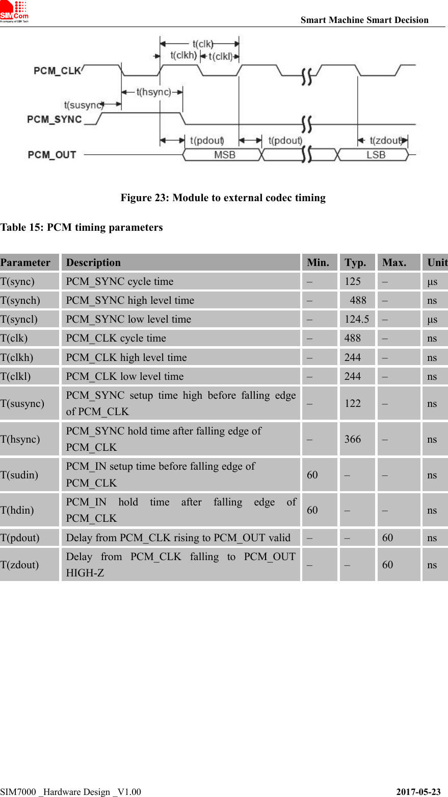
![3.6 PCM InterfaceSIM7000 provides a PCM interface for external codec, which can be used in master mode withshort sync and 16 bits linear format.Table 14: PCM formatNote: For more details about PCM AT commands, please refer to document [1].3.6.1 PCM timingSIM7000 supports 2.048 MHz PCM data and sync timing for 16 bits linear format codec.Figure 21: PCM_SYNC timingFigure 22: External codec to module timingCharacteristicsSpecificationLine Interface FormatLinear(Fixed)Data length16bits(Fixed)PCM Clock/Sync SourceMaster Mode(Fixed)PCM Clock Rate2048 KHz (Fixed)PCM Sync FormatShort sync(Fixed)Data OrderingMSB](https://usermanual.wiki/SIMCom-Wireless-Solutions/SIM7000A.SIM7000A-User-Manual-V1-00/User-Guide-4125651-Page-32.png)
![Smart Machine Smart DecisionSIM7000 _Hardware Design _V1.00 2017-05-233.6.2 PCM Application GuideThe following figure shows the external codec reference design.Figure 24: Audio codec reference circuit3.7 I2C InterfaceSIM7000 provides a I2C interface compatible with I2C specification, version 5.0, with clock rateup to 400 kbps. Its operation voltage is 1.8V.The following figure shows the I2C bus reference design.Figure 25: I2C reference circuitNote:I2C_SDA and I2C_SCL do not have pull-up resistors in module. So the two externalpulling up resistors are needed in application circuit.“AT+CRIIC and AT+CWIIC” AT commands could be used to read/write register values of theI2C peripheral devices. For more details about AT commands please refer to document [1].3.8 Network statusThe NETLIGHT pin is used to control Network Status LED, its reference circuit is shown in the](https://usermanual.wiki/SIMCom-Wireless-Solutions/SIM7000A.SIM7000A-User-Manual-V1-00/User-Guide-4125651-Page-34.png)
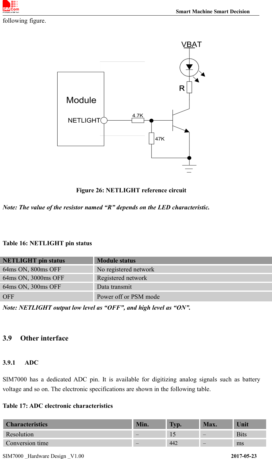
![Smart Machine Smart DecisionSIM7000 _Hardware Design _V1.00 2017-05-23Input Range0.11.7VInput serial resistance1––MΩNote: “AT+CADC” can be used to read the voltage of the ADC pin, for more details, please referto document [1].3.9.2 LDOSIM7000 has a LDO power output named VDD_EXT. The output voltage is 1.8V.Figure 27:Power on sequence of the VDD_EXTTable 18: Electronic characteristicSymbolDescriptionMin.Typ.Max.UnitVVDD_EXTOutput voltage1.71.81.9VIOOutput current--50mANote:The VDD_EXT is used to the IO power in the module. The Output voltage is not supportedto set.](https://usermanual.wiki/SIMCom-Wireless-Solutions/SIM7000A.SIM7000A-User-Manual-V1-00/User-Guide-4125651-Page-36.png)
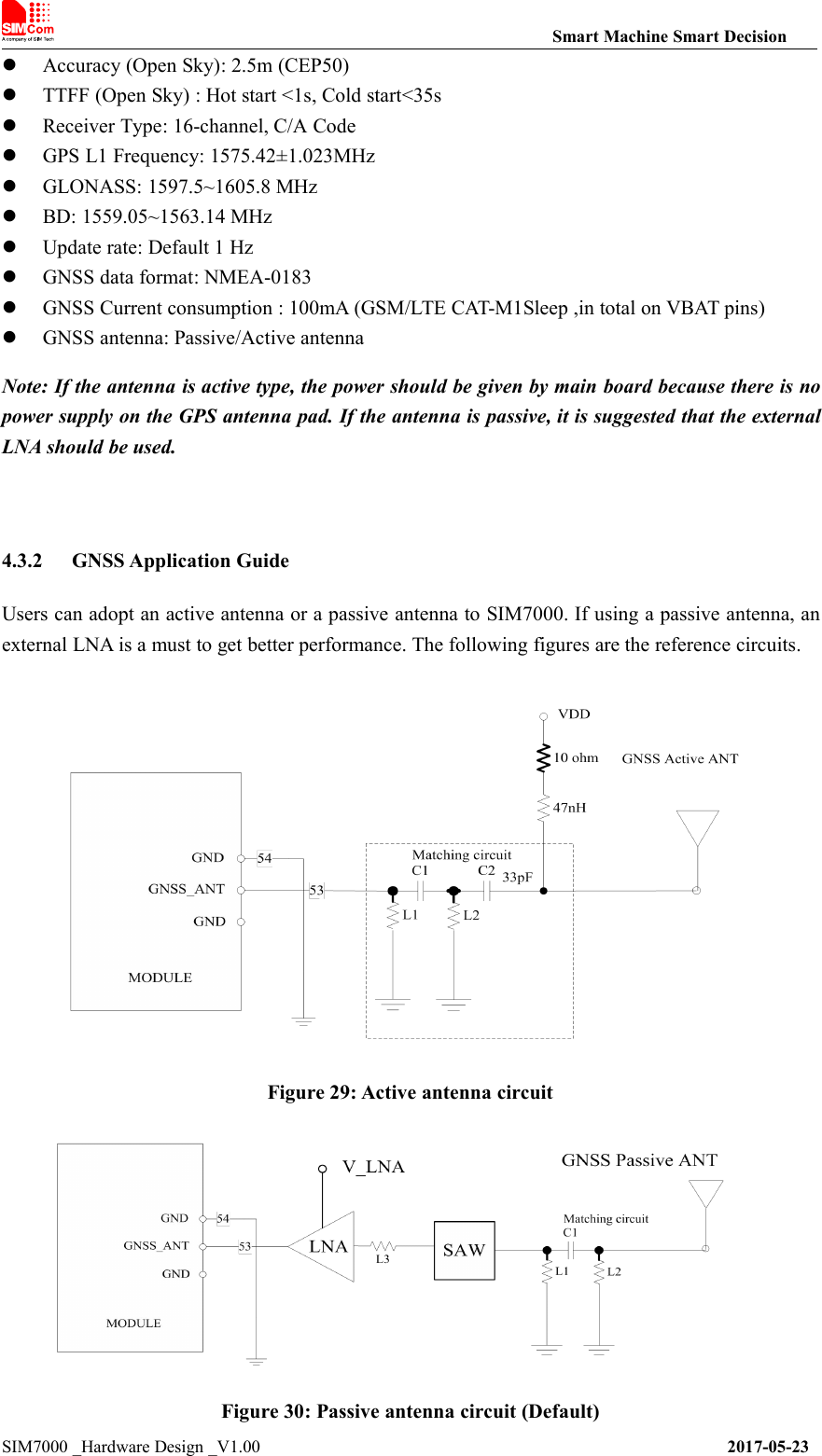
![Smart Machine Smart DecisionSIM7000 _Hardware Design _V1.00 2017-05-23In above figures, the components C1, L1 and L2 are used for antenna matching. Usually, the valuesof the components can only be achieved after antenna tuning and usually provided by antennavendor. C2 is used for DC blocking. L3 is the matching component of the external LNA, and thevalue of L3 is determined by the LNA characteristic and PCB layout. Both VDD of active antennaand V_LNA need external power supplies which should be considered according to active antennaand LNA characteristic. LDO/DCDC is recommended to get lower current consuming by shuttingdown active antennas and LNA when GNSS is not working.GNSS can be tested by NMEA port. NMEA sentences can be obtained through UART or USBautomatically. NMEA sentences include GSV, GGA, RMC, GSA, and VTG. Before using GNSS,user should configure SIM7000 in proper operating mode by AT command. Please refer to relateddocuments for details. SIM7000 can also get position location information through AT directly.Note:1. GNSS is closed by default and can be started by “AT+CGNSPWR=1”. The AT command hastwo parameters, the first is on/off, and the second is GNSS mode. Default mode is standalonemode.AGPS mode needs more support from the mobile telecommunication network. Please refer todocument [24] for more details.2. If the passive antenna is used, put the LNA close to the antenna.3. Make sure there are no noise signals around GNSS antenna.](https://usermanual.wiki/SIMCom-Wireless-Solutions/SIM7000A.SIM7000A-User-Manual-V1-00/User-Guide-4125651-Page-43.png)
![Smart Machine Smart DecisionSIM7000 _Hardware Design _V1.00 2017-05-23than normal mode.Flight modeAT command “AT+CFUN=4” can be used to set the module to flightmode without removing the power supply. In this mode, the RF partof the module will not work, but the serial port and USB port are stillaccessible. The power consumption in this mode is lower than normalmode.PSM modeSetting the timer of the software can be entered PSM mode. In thismode, the module will be the least current consumption. Meanwhile,all the output of the LDO and DCDC in the module will be closedexcept the RTC power. And also all of the functions will beunavailable except the RTC function. RTC timer can wake up themodule.Power off modeModule will go into power off mode by sending the AT command“AT+CPOWD” or pull down the PWRKEY pin, normally. In thismode the power management unit shuts down the power supply, andsoftware is not active. The serial port and USB are is not accessible.5.3.2 Sleep modeIn sleep mode, the current consumption of module will be reduced to the minimal level, andmodule can still receive paging message and SMS.Several hardware and software conditions must be satisfied together in order to let SIM7000 entersleep mode:1. UART condition2. USB condition3. Software conditionNote: Before designing, pay attention to how to realize sleeping/waking function and refer toDocument [26] for more details.5.3.3 Minimum functionality mode and Flight modeMinimum functionality mode ceases a majority function of the module, thus minimizing the powerconsumption. This mode is set by the AT command which provides a choice of the functionalitylevels.●AT+CFUN=0: Minimum functionality●AT+CFUN=1: Full functionality (Default)●AT+CFUN=4: Flight modeIf SIM7000 has been set to minimum functionality mode, the RF function and SIM card functionwill be closed. In this case, the serial port and USB are still accessible, but RF function and SIMcard will be unavailable.If SIM7000 has been set to flight mode, the RF function will be closed. In this case, the serial portand USB are still accessible, but RF function will be unavailable.](https://usermanual.wiki/SIMCom-Wireless-Solutions/SIM7000A.SIM7000A-User-Manual-V1-00/User-Guide-4125651-Page-46.png)
![Smart Machine Smart DecisionSIM7000 _Hardware Design _V1.00 2017-05-236.3 Typical SMT Reflow ProfileSIMCom provides a typical soldering profile. Therefore the soldering profile shown below is onlya generic recommendation and should be adjusted to the specific application and manufacturingconstraints.Figure 33: The ramp-soak-spike reflow profile of SIM7000Note: For more details about secondary SMT, please refer to the document [21].6.4 Moisture Sensitivity Level (MSL)SIM7000 is qualified to Moisture Sensitivity Level (MSL) 3 in accordance with JEDEC J-STD-033.If the prescribed time limit is exceeded, users should bake modules for 192 hours in dryingequipment (<5% RH) at 40+5/-0°C, or 72 hours at 85+5/-5°C. Note that plastic tray is notheat-resistant, and only can be baked at 45° C.Table 34: Moisture Sensitivity Level and Floor LifeMoisture Sensitivity Level(MSL)Floor Life (out of bag) at factory ambient≤30°C/60% RH or asstated1Unlimited at ≦30℃/85% RH21 year2a4 weeks3168 hours472 hours548 hours5a24 hours6Mandatory bake before use. After bake, it must be reflowed within the](https://usermanual.wiki/SIMCom-Wireless-Solutions/SIM7000A.SIM7000A-User-Manual-V1-00/User-Guide-4125651-Page-51.png)
![Smart Machine Smart DecisionSIM7000 _Hardware Design _V1.00 2017-05-23B. Related DocumentsTable 38: Related DocumentsNO.TitleDescription[1]SIM7X00 Series_ATCommand Manual_V1.xxAT Command Manual[2]ITU-T Draft newrecommendationV.25terSerial asynchronous automatic dialing and control[3]GSM 07.07Digital cellular telecommunications (Phase 2+); AT commandset for GSM Mobile Equipment (ME)[4]GSM 07.10Support GSM 07.10 multiplexing protocol[5]GSM 07.05Digital cellular telecommunications (Phase 2+); Use of DataTerminal Equipment – Data Circuit terminating Equipment(DTE – DCE) interface for Short Message Service (SMS)and Cell Broadcast Service (CBS)[6]GSM 11.14Digital cellular telecommunications system (Phase 2+);Specification of the SIM Application Toolkit for theSubscriber Identity Module – Mobile Equipment (SIM – ME)interface[7]GSM 11.11Digital cellular telecommunications system (Phase 2+);Specification of the Subscriber Identity Module – MobileEquipment (SIM – ME) interface[8]GSM 03.38Digital cellular telecommunications system (Phase 2+);Alphabets and language-specific information[9]GSM 11.10Digital cellular telecommunications system (Phase 2) ;Mobile Station (MS) conformance specification ;Part 1:Conformance specification[10]3GPP TS 51.010-1Digital cellular telecommunications system (Release 5);Mobile Station (MS) conformance specification[11]3GPP TS 34.124Electromagnetic Compatibility (EMC) for mobile terminalsand ancillary equipment.[12]3GPP TS 34.121Electromagnetic Compatibility (EMC) for mobile terminalsand ancillary equipment.[13]3GPP TS 34.123-1Technical Specification Group Radio Access Network;Terminal conformance specification; Radio transmission andreception (FDD)[14]3GPP TS 34.123-3User Equipment (UE) conformance specification; Part 3:Abstract Test Suites.[15]EN 301 908-02 V2.2.1Electromagnetic compatibility and Radio spectrum Matters(ERM); Base Stations (BS) and User Equipment (UE) forIMT-2000. Third Generation cellular networks; Part 2:Harmonized EN for IMT-2000, CDMA Direct Spread(UTRA FDD) (UE) covering essential requirements of article3.2 of the R&TTE Directive[16]EN 301 489-24 V1.2.1Electromagnetic compatibility and Radio Spectrum Matters(ERM); Electromagnetic Compatibility (EMC) standard forradio equipment and services; Part 24: Specific conditions forIMT-2000 CDMA Direct Spread (UTRA) for Mobile andportable (UE) radio and ancillary equipment[17]IEC/EN60950-1(2001)Safety of information technology equipment (2000)](https://usermanual.wiki/SIMCom-Wireless-Solutions/SIM7000A.SIM7000A-User-Manual-V1-00/User-Guide-4125651-Page-57.png)
![Smart Machine Smart DecisionSIM7000 _Hardware Design _V1.00 2017-05-23[18]3GPP TS 51.010-1Digital cellular telecommunications system (Release 5);Mobile Station (MS) conformance specification[19]GCF-CC V3.23.1Global Certification Forum - Certification Criteria[20]2002/95/ECDirective of the European Parliament and of the Council of27 January 2003 on the restriction of the use of certainhazardous substances in electrical and electronic equipment(RoHS)[21]Modulesecondary-SMT-UGD-V1.xxModule secondary SMT Guidelines[22]SIM7X00Series_UART_ApplicationNote_V1.xxThis document describes how to use UART interface ofSIMCom modules.[23]SIM7X00 Series_USBAUDIO_ApplicationNote_V1.xxUSB AUDIO Application Note[24]SIM7X00Series_GPS_ApplicationNote_V1.xxGPS Application Note[25]Antenna design guidelines fordiversity receiver systemAntenna design guidelines for diversity receiver system[26]SIM7X00 Series_Sleep Mode_Application Note_V1.xxSleep Mode Application Note](https://usermanual.wiki/SIMCom-Wireless-Solutions/SIM7000A.SIM7000A-User-Manual-V1-00/User-Guide-4125651-Page-58.png)