ST Microelectronics S R L SP1ML SPIRIT1 915 MHz Low Power RF Module User Manual Spirit 1 Module Datasheet
ST Microelectronics S.R.L. SPIRIT1 915 MHz Low Power RF Module Spirit 1 Module Datasheet
Users Manual
ST CONFIDENTIAL
February 2014
Doc ID TBD Rev 0.8 Rev 0.8
1/19
www.st.com
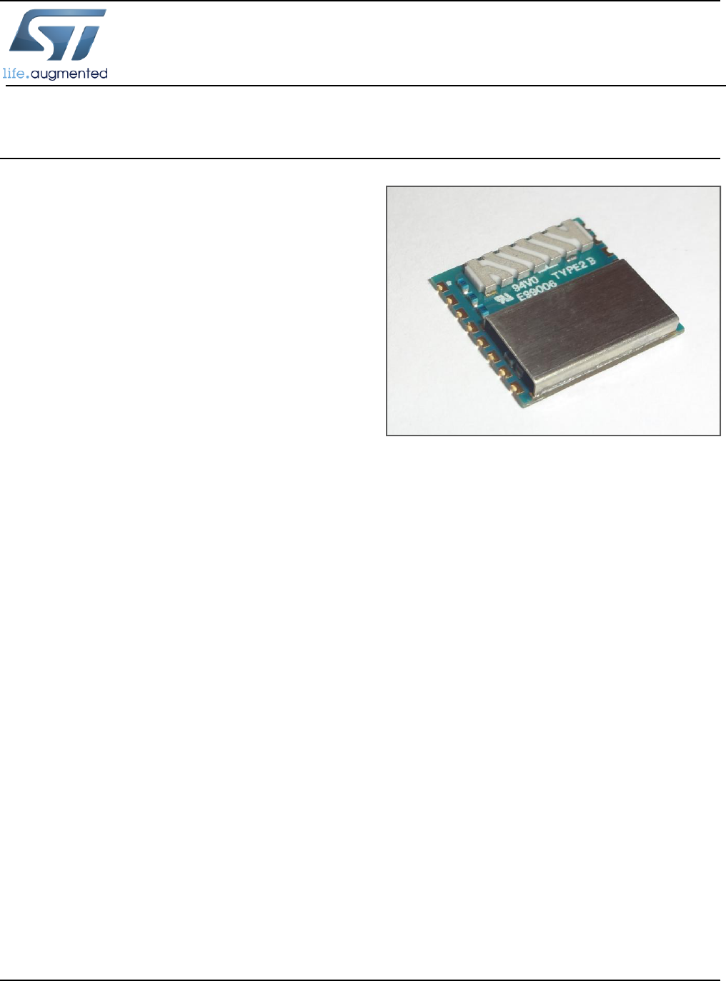
SPLML-868 and SP1ML-915
SPIRIT1 868 and 915 MHz Low Power RF Modules
PRELIMINARY DATASHEET
Features
Complete RF ready Spirit1 module
Integrated antenna and crystal
STM32L microcontroller up to 32 MHz
Low power consumption
UART interface with AT command set
Operates from a single 1.8V to 3.6V supply
863 to 870 MHz operation (SP1ML-868)
902 to 928 MHz operation (SP1ML-915)
Output power up to +11.6dBm
Data rates up to 500kbps
Modulation schemes: 2-FSK, GFSK, GMSK,
OOK, and ASK
Compact size: 14mm x 13.4mm x 2.5mm
Operating temperature: -40 °C to 85 °C
FCC and CE regulatory approvals
Applications
Serial cable replacement
Home automation
M2M industrial control
Service diagnostic
Data acquisition equipment
Machine control
Sensor monitoring
Security systems
Mobile health and medical

2/19
Doc ID TBD Rev 0.8 Rev 0.1
www.st.com
Contents
1 Description ........................................................................................... 4
2 Hardware specification........................................................................ 5
2.1 Recommended operating conditions ......................................................................... 5
2.2 Absolute maximum ratings ........................................................................................ 5
2.3 I/O operating characteristics ..................................................................................... 5
2.4 Current consumption ................................................................................................. 6
2.5 RF compliance limits ................................................................................................. 6
2.6 Pin assignment ......................................................................................................... 7
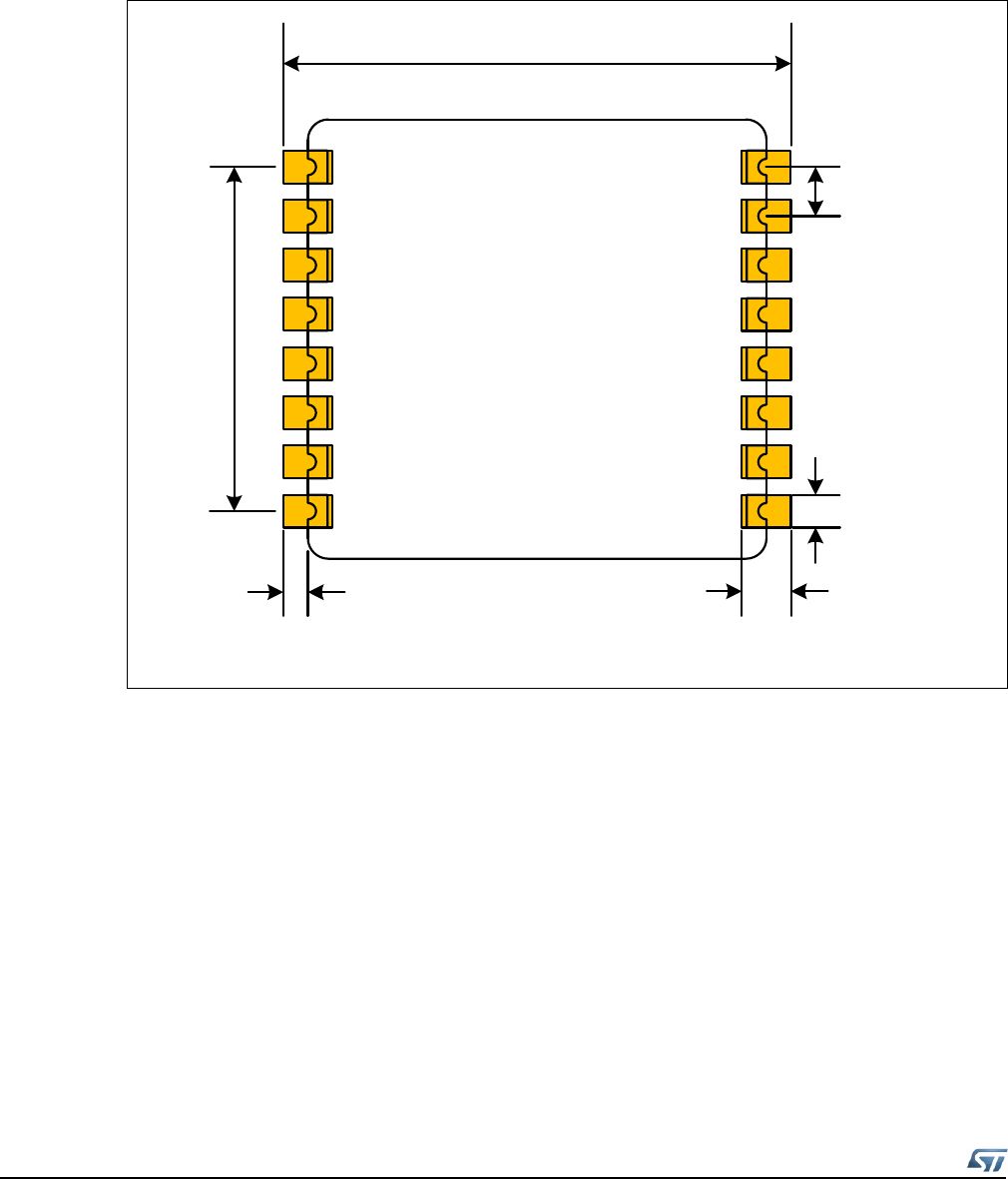
2.7 Pin placement ........................................................................................................... 8
2.8 Hardware block diagram ........................................................................................... 8
3 Hardware design .................................................................................. 9
3.1 Pin usage .................................................................................................................. 9
3.2 Typical application circuit ........................................................................................ 10
3.3 Layout guidelines .................................................................................................... 11
3.4 Recommended footprint .......................................................................................... 12
3.5 Module reflow installation ........................................................................................ 13
4 Mechanical data ................................................................................. 14
4.1 RoHS compliance ................................................................................................... 14
5 Regulatory compliance ..................................................................... 15
5.1 FCC certification ..................................................................................................... 15
5.2 CE certification ........................................................................................................ 15
5.3 Labeling instructions ............................................................................................... 16
5.4 Product manual instructions .................................................................................... 16
6 Ordering Information ......................................................................... 18

Doc ID TBD Rev 0.8 Rev 0.1
3/19
www.st.com
List of tables
Table 1. Recommended operating conditions .................................................................................... 5
Table 2. Absolute maximum ratings ................................................................................................... 5
Table 3. I/O operating characteristics ................................................................................................. 5
Table 4. Current consumption ............................................................................................................ 6
Table 5. RF compliance limits ............................................................................................................ 6
Table 6. Pin assignment ..................................................................................................................... 7
Table 7. Module pin usage ................................................................................................................. 9
Table 8. Soldering profile ................................................................................................................. 13
Table 12. Ordering information ....................................................................................................... 18
List of figures
Figure 1. Pin placement ...................................................................................................................... 8
Figure 2. Hardware block diagram ...................................................................................................... 8
Figure 3. Typical application circuit ................................................................................................... 10
Figure 4. Layout guidelines ............................................................................................................... 11
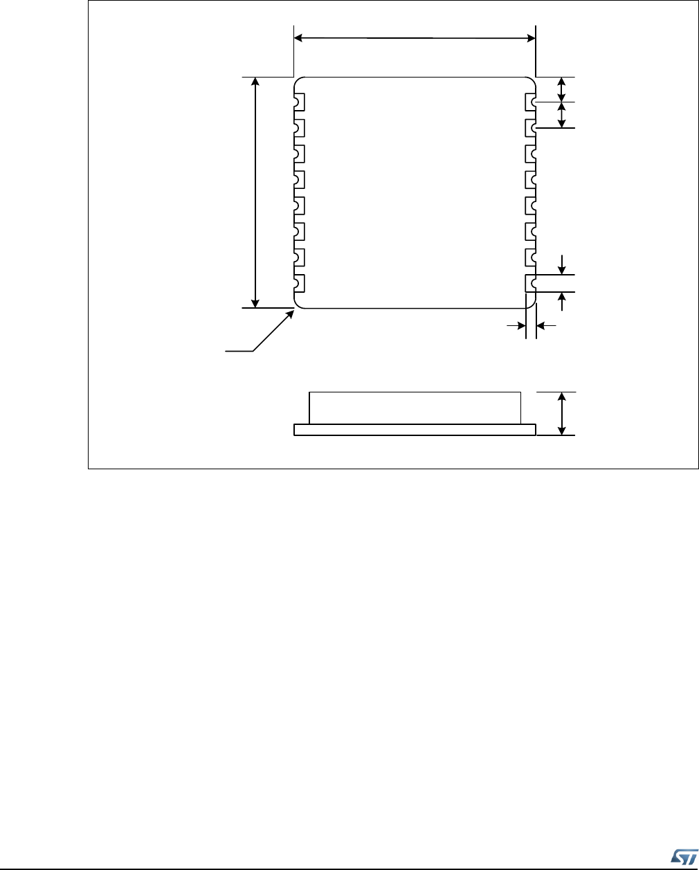
Figure 5. Recommended footprint ..................................................................................................... 12
Figure 6. Soldering profile ................................................................................................................. 13
Figure 7. Mechanical data ................................................................................................................. 14

4/19
Doc ID TBD Rev 0.8 Rev 0.1
www.st.com
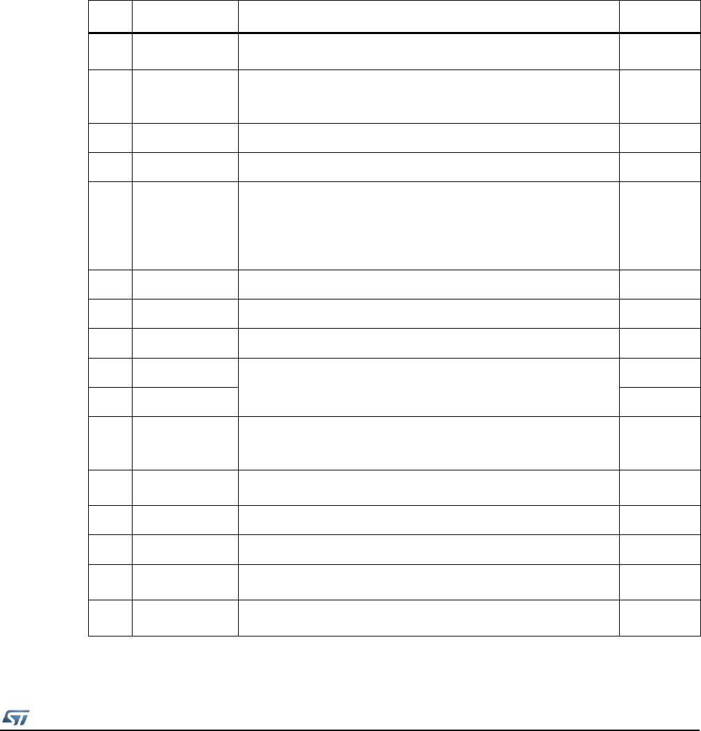
1 Description
The SP1ML-868 and SP1ML-915 are low power RF modules based on the SPIRIT1 radio,
with integrated voltage regulation, antenna, crystal and microcontroller in a compact
surface mount module form-factor. The module allows OEMs to easily add wireless
capability to any electronic device without requiring in-depth RF experience, and has the
necessary FCC modular approvals and CE compliance to reduce time to market.
The UART host interface allows simple connection to an external microcontroller. Access
to module features is provided through an extended AT command set. A simple cable
replacement model allows the module to be used similarly to a standard serial interface.
The microcontroller serial wire debug signals are available and allow the standard
firmware to be replaced by a user application, enabling use as a wireless application
module where no external microprocessor system is required. Select STM32L GPIO and
peripherals are available for interfacing to external devices in the user application, and
advanced features of the SPIRIT1 radio are also accessible.
Doc ID TBD Rev 0.8 Rev 0.1
5/19
www.st.com
2 Hardware specification
General conditions (VIN = 3 V and TA = 25˚C).
2.1 Recommended operating conditions
Table 1. Recommended operating conditions
Symbol
Parameter
Min.
Typ.
Max.
Unit
TA
Operating ambient temperature range
-40
-
85
˚C
VDD
Operating supply voltage
1.8
3
3.6
V
FREQ
RF frequency (SP1ML-868)
863
-
870
MHz
FREQ
RF frequency (SP1ML-915)
902
-
928
MHz
2.2 Absolute maximum ratings
Table 2. Absolute maximum ratings
Symbol
Parameter
Min.
Typ.
Max.
Unit
TSTG
Storage temperature range
-40
-
85
˚C
VDD
Operating supply voltage
-0.3
-
3.9
V
VIO
I/O pin voltage
-0.3
-
5.5
V
2.3 I/O operating characteristics
Table 3. I/O operating characteristics
Symbol
Parameter
Min.
Typ.
Max.
Unit
VIL(1)
I/O input low level voltage
-0.3
-
0.3 VDD
V
VIH(1)
I/O input high level voltage
0.7 VIN
-
VDD+0.3
V
1. For more details see the STM32L151RB datasheet, I/O port characteristics.
6/19
Doc ID TBD Rev 0.8 Rev 0.1
www.st.com
2.4 Current consumption
Table 4. Current consumption
Symbol
Parameter
Test Conditions
Typ.
Unit
IDD
Supply current
Operating mode
Tx, +11dBm, 2-FSK, 915 MHz
20
mA
Operating mode
Tx, -7dBm, 2-FSK, 915 MHz
8
mA
Operating mode
Rx, 915 MHz
11
mA
Operating mode – Idle
800
µA
Command mode
1.3
mA
Standby
1.4
µA
2.5 RF compliance limits
The RF compliance limits are those tested for FCC and CE certification. These limits are
enforced by the factory loaded firmware.
Table 5. RF compliance limits
Modulation
Standards
Parameter
Max.
Unit
2-FSK
GFSK
MSK
FCC Part 15.207 (1)
FCC Part 15.247 (1)
EN 300 220-2 V2.4.1 (2)
EN 301 489-01 V1.9.2 (2)
EN 301 489-03 V1.4.1 (2)
Data rate
500
kbps
Output power
+11.6
dBm
OOK
ASK
FCC Part 15.207 (1)
FCC Part 15.249 (1)
EN 300 220-2 V2.4.1 (2)
EN 301 489-01 V1.9.2 (2)
EN 301 489-03 V1.4.1 (2)
Data rate
250
kbps
Output power
+8.5
dBm
1. FCC standards are only applicable to the SP1ML-915 module.
2. EN standards are only applicable to the SP1ML-868 module.
Doc ID TBD Rev 0.8 Rev 0.1
7/19
www.st.com
2.6 Pin assignment
Table 6. Pin assignment
Pin
Name
Type
Description
STM32L pin(1)
1
TXRXLED
O
Active low Tx/Rx LED drive
PA2
2
WKUP
I/O
Wake up module from shutdown
PA0
3
GPIO0
I/O
General purpose input/output 0
PB15
4
GPIO1
I/O
General purpose input/output 1
PB14
5
MODE0
I/O
Protocol mode selection 0(2)
PB13
6
MODE1
I/O
Protocol mode selection 1(2)
PB12
7
VDD
Power
Supply input voltage
-
8
GND
Power
Ground
-
9
SWDIO
I/O
Serial wire I/O
PA13
10
SWCLK
I
Serial wire clock
PA14
11
BOOTMODE
I
Boot mode selection
BOOT0
12
RESET
I
Reset input, active low
NRST
13
TXD
O
UART transmit data
PA9
14
RXD
I
UART receive data
PA10
15
RTS
O
UART request to send
PB6
16
CTS
I
UART clear to send
PB7
1. For more details see the STM32L151RB datasheet, Pin descriptions section. Alternate functions of any
given pin are dependent on the user application firmware that is loaded into the module and is beyond the
scope of the document.
2. Refer to Hardware design section for details of protocol mode selection.
Doc ID TBD Rev 0.8 Rev 0.1
9/19
www.st.com
3 Hardware design
3.1 Pin usage
If used with the default firmware and interfaced to a host MCU, at a minimum the SP1ML
module requires power, ground and UART transmit and receive signals to be connected.
Other signals are optional and provide additional functionality. These signals are outlined
in the following table. Unused signals must not be connected.
Table 7. Module pin usage
Pin
Name
Description
Optional
1
TXRXLED
An active-low open drain output that can drive an
external LED for TX/RX activity status indication.
Yes
2
WKUP
Drive this signal low to put the module into a low
power shutdown mode. Float or drive the signal high
to wake the module.
Yes
3
GPIO0
Reserved for future use, do not connect.
Yes
4
GPIO1
Reserved for future use, do not connect.
Yes
5
MODE0
Drive this signal low to force the module into
operating mode. Drive this signal high to force the
module into command mode. This enables faster
switching between modes and obviates the need for
escape sequences.
Yes
6
MODE1
Reserved for future use, do not connect.
Yes
7
VDD
Connect to power supply, 1.8V to 3.6V.
No
8
GND
Connect to system ground.
No
9
SWDIO
These signals are the serial wire debug (SWD)
interface to the STM32L microcontroller, supporting
the development and loading of custom firmware.
Yes
10
SWCLK
Yes
11
BOOTMODE
Drive this signal high at power up or reset to start the
boot loader and allow device firmware update over
the UART interface.
Yes
12
RESET
Drive this signal low to hold the module in reset. Drive
this signal high to release the module from reset.
Yes
13
TXD
Connect to the host system UART RXD input.
No
14
RXD
Connect to the host system UART TXD output.
No
15
RTS
Connect to the host system UART CTS output if flow
control is required.
Yes
16
CTS
Connect to the host system UART RTS input if flow
control is required.
Yes
10/19
Doc ID TBD Rev 0.8 Rev 0.1
www.st.com
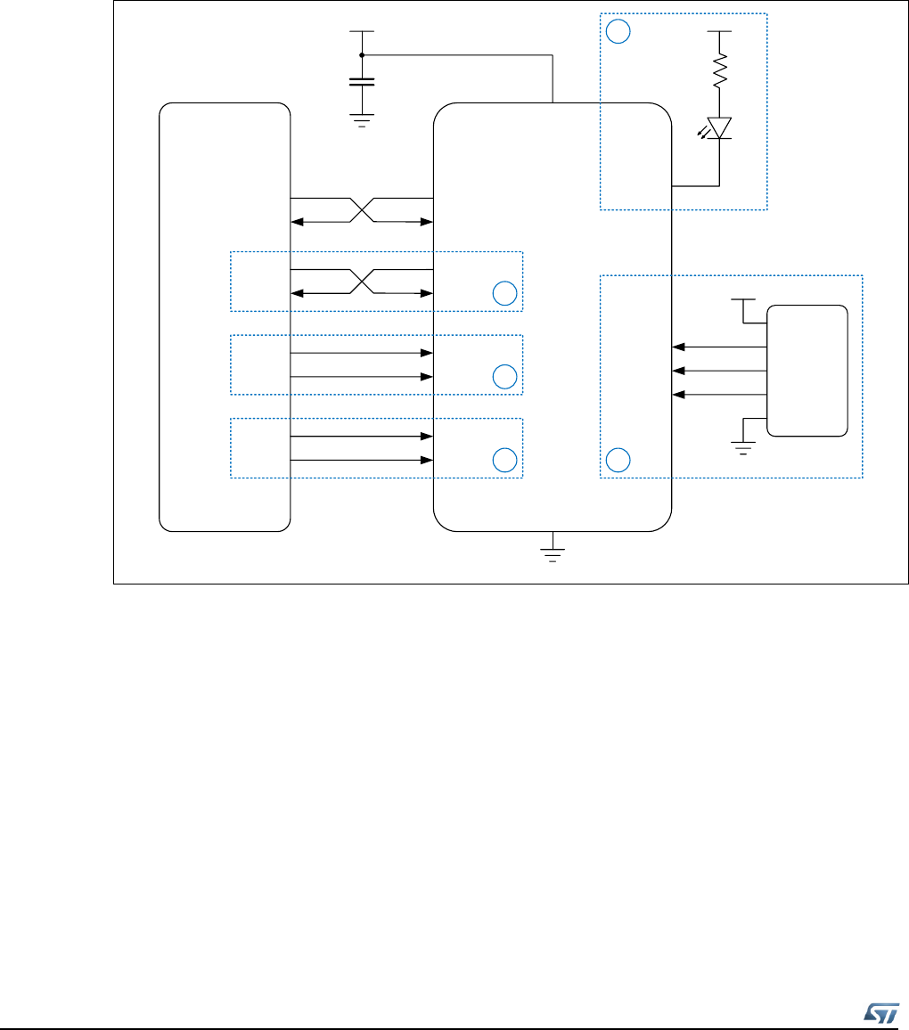
3.2 Typical application circuit
In a typical application the SP1ML module is connected to a host MCU using a standard
UART, with transmit and receive signals. This is illustrated in the following diagram.
Figure 3. Typical application circuit
SP1ML
MODULE
HOST
MCU
TXD TXD
RXD RXD
RTS RTS
CTS CTS
GPIO
GPIO
BOOTMODE
RESET
GPIO
GPIO
MODE0
WKUP
TXRXLED
1
2
3
4
VDD
RESET
SWCLK
SWDIO
5
SWD
HEADER
VDD
VDD
VDD
GND
10uF
Optional Functionality
1. The TXRXLED signal is an active-low open drain output that can be used to drive an
external LED for status indication when data is sent or received.
2. The RTS and CTS signals can be connected to the host UART interface if hardware
flow control is required.
3. The MODE0 signal provides a hardware method for switching between command and
operating modes. The WKUP signal allows the module to be placed into a low power
shutdown mode and woken up again.
4. The BOOTMODE AND RESET signals should be connected if module firmware will
need to be updated over the UART interface.
5. To support custom module firmware, the serial wire debug signals need to be
accessible for programming and debugging.
Doc ID TBD Rev 0.8 Rev 0.1
11/19
www.st.com
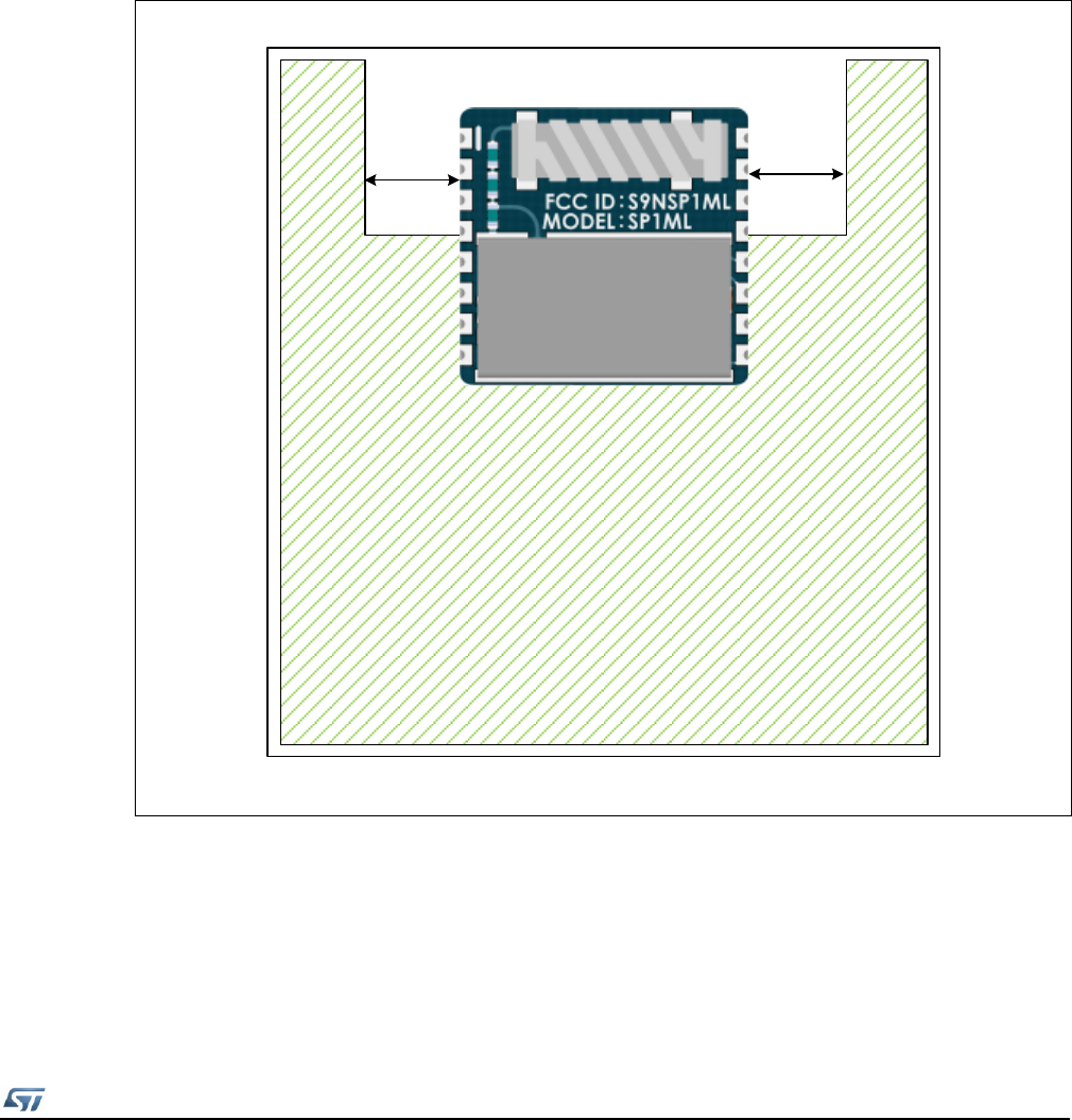
3.3 Layout guidelines
The application PCB requires a flooded ground plane. Care must be taken to ensure
there are no traces or ground planes under the area surrounding the antenna, with the
exception of minimal width traces from pins 1,2,3,4,13,14,15 and 16 of the module if these
are used. It is appropriate to place the module toward the edge of the PCB with no traces
or ground planes from the antenna to the board edge.
Figure 4. Layout guidelines
Application PCB
No copper on any layer surrounding antenna, except
minimal traces from pins 1,2,3,4,13,14,15 and 16
Flooded ground plane required
(signal traces allowed)
min .
6 mm min .
6 mm
Doc ID TBD Rev 0.8 Rev 0.1
13/19
www.st.com
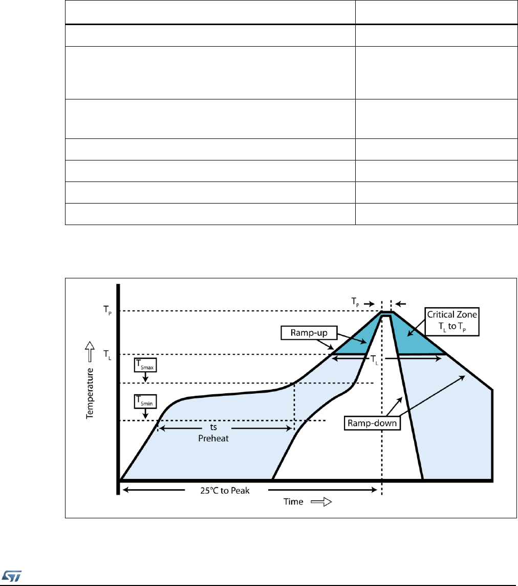
3.5 Module reflow installation
The SP1ML is a surface mount module supplied on a 16-pin, 4-layer PCB. The final
assembly recommended reflow profile is indicated below, based on IPC/JEDEC JSTD-
020C, July 2004 recommendations.
Table 8. Soldering profile
Profile feature
Lead-free assembly
Average ramp-up rate (TSMAX to TP)
3 °C/sec max
Preheat:
– Temperature min. (TS min.)
– Temperature max. (TS max.)
– Time (ts min. to ts max.)(ts)
150 °C
200 °C
60-100 sec
Time maintained above:
– Temperature TL
– Temperature TL
217 °C
60-70 sec
Peak temperature (TP)
240 °C
Time within 5 °C of actual peak temperature (TP)
10-20 sec
Ramp-down rate
6 °C/sec
Time from 25 °C to peak temperature
8 minutes max.
Figure 6. Soldering profile

Doc ID TBD Rev 0.8 Rev 0.1
15/19
www.st.com
5 Regulatory compliance
5.1 FCC certification
This module has been tested and found to comply with the FCC part 15 rules. These limits
are designed to provide reasonable protection against harmful interference in approved
installations. This equipment generates, uses, and can radiate radio frequency energy
and, if not installed and used in accordance with the instructions, may cause harmful
interference to radio communications.
However, there is no guarantee that interference may not occur in a particular installation.
This device complies with part 15 of the FCC rules. Operation is subject to the following
two conditions: (1) This device may not cause harmful interference, and (2) this device
must accept any interference received, including interference that may cause undesired
operation.
Modifications or changes to this equipment not expressly approved by STMicroelectronics
may render void the user's authority to operate this equipment.
Modular approval
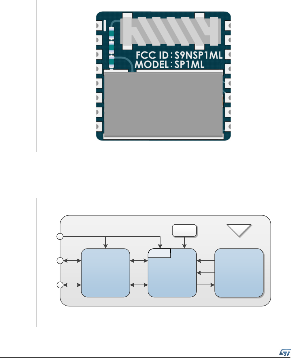
FCC ID: S9NSP1ML
In accordance with FCC part 15, the SP1ML-915 is listed as a modular transmitter device.
This module is evaluated for stand-alone use only. Finished products incorporating
multiple transmitters must comply with colocation and RF exposure requirements in
accordance with FCC multi-transmitter product procedures. Collocated transmitters
operating in portable RF Exposure conditions (e.g. <20cm from persons including but not
limited to body worn and hand held devices) may require separate approval.
5.2 CE certification
The module has been certified according to the following standards:
EN 300 220-2 V2.4.1
EN 301 489-01 V1.9.2
EN 301 489-03 V1.4.1

16/19
Doc ID TBD Rev 0.8 Rev 0.1
www.st.com
5.3 Labeling instructions
When integrating the SP1ML-915 into the final product, the OEM must ensure that the
FCC labeling requirements are satisfied. A statement must be included on the exterior of
the final product which indicates the product includes a certified module. The label should
state the following (or similar wording that conveys the same meaning):
Contains FCC ID: S9NSP1ML
OR This product contains FCC ID: S9NSP1ML
The OEM must include the following statements on the exterior of the final product unless
the product is too small (e.g. less than 4 x 4 inches):
This device complies with Part 15 of the FCC Rules. Operation is subject to the
following two conditions: (1) this device may not cause harmful interference, and
(2) this device must accept any interference received, including any interference
that may cause undesired operation.
5.4 Product manual instructions
This section applies to OEM final products containing the SP1ML-915 module, subject to
FCC compliance. The final product manual must contain the following statement (or a
similar statement that conveys the same meaning):
WARNING: Changes or modifications not expressly approved by the party
responsible for compliance could void the user’s authority to operate the equipment
In the case where an OEM seeks Class B (residential) limits for the final product, the
following statement must be included in the final product manual:
NOTE: This equipment has been tested and found to comply with the limits for a
Class B digital device, pursuant to part 15 of the FCC Rules. These limits are
designed to provide reasonable protection against harmful interference in a
residential installation. This equipment generates, uses and can radiate radio
frequency energy and, if not installed and used in accordance with the instructions,
may cause harmful interference to radio communications. However, there is no
guarantee that interference will not occur in a particular installation. If this
equipment does cause harmful interference to radio or television reception, which
can be determined by turning the equipment off and on, the user is encouraged to
try to correct the interference by one or more of the following measures:
Reorient or relocate the receiving antenna.
Increase the separation between the equipment and receiver.
Connect the equipment into an outlet on a circuit different from that to which the
receiver is connected.
Consult the dealer or an experienced radio/TV technician for help.

Doc ID TBD Rev 0.8 Rev 0.1
17/19
www.st.com
In the case where an OEM seeks the lesser category of a Class A digital device for the
final product, the following statement must be included in the final product manual:
NOTE: This equipment has been tested and found to comply with the limits for a
Class A digital device, pursuant to part 15 of the FCC Rules. These limits are
designed to provide reasonable protection against harmful interference when the
equipment is operated in a commercial environment. This equipment generates,
uses, and can radiate radio frequency energy and, if not installed and used in
accordance with the instruction manual, may cause harmful interference to radio
communications. Operation of this equipment in a residential area is likely to cause
harmful interference in which case the user will be required to correct the
interference at his expense.


Doc ID TBD Rev 0.8 Rev 0.1
19/19
www.st.com
Please Read Carefully:
Information in this document is provided solely in connection with ST products. STMicroelectronics NV and its subsidiaries (“ST”) reserve the
right to make changes, corrections, modifications or improvements, to this document, and the products and services described herein at any
time, without notice.
All ST products are sold pursuant to ST’s terms and conditions of sale.
Purchasers are solely responsible for the choice, selection and use of the ST products and services described herein, and ST assumes no
liability whatsoever relating to the choice, selection or use of the ST products and services described herein.
No license, express or implied, by estoppel or otherwise, to any intellectual property rights is granted under this document. If any part of this
document refers to any third party products or services it shall not be deemed a license grant by ST for the use of such third party products or
services, or any intellectual property contained therein or considered as a warranty covering the use in any manner whatsoever of such third
party products or services or any intellectual property contained therein.
UNLESS OTHERWISE SET FORTH IN ST’S TERMS AND CONDITIONS OF SALE ST DISCLAIMS ANY EXPRESS OR IMPLIED
WARRANTY WITH RESPECT TO THE USE AND/OR SALE OF ST PRODUCTS INCLUDING WITHOUT LIMITATION IMPLIED
WARRANTIES OF MERCHANTABILITY, FITNESS FOR A PARTICULAR PURPOSE (AND THEIR EQUIVALENTS UNDER THE LAWS OF
ANY JURISDICTION), OR INFRINGEMENT OF ANY PATENT, COPYRIGHT OR OTHER INTELLECTUAL PROPERTY RIGHT.
UNLESS EXPRESSLY APPROVED IN WRITING BY TWO AUTHORIZED ST REPRESENTATIVES, ST PRODUCTS ARE NOT
RECOMMENDED, AUTHORIZED OR WARRANTED FOR USE IN MILITARY, AIR CRAFT, SPACE, LIFE SAVING, OR LIFE SUSTAINING
APPLICATIONS, NOR IN PRODUCTS OR SYSTEMS WHERE FAILURE OR MALFUNCTION MAY RESULT IN PERSONAL INJURY,
DEATH, OR SEVERE PROPERTY OR ENVIRONMENTAL DAMAGE. ST PRODUCTS WHICH ARE NOT SPECIFIED AS "AUTOMOTIVE
GRADE" MAY ONLY BE USED IN AUTOMOTIVE APPLICATIONS AT USER’S OWN RISK.
Resale of ST products with provisions different from the statements and/or technical features set forth in this document shall immediately void
any warranty granted by ST for the ST product or service described herein and shall not create or extend in any manner whatsoever, any
liability of ST.
ST and the ST logo are trademarks or registered trademarks of ST in various countries.
Information in this document supersedes and replaces all information previously supplied.
The ST logo is a registered trademark of STMicroelectronics. All other names are the property of their respective owners.
© 2014 STMicroelectronics - All rights reserved
STMicroelectronics group of companies
Australia - Belgium - Brazil - Canada - China - Czech Republic - Finland - France - Germany - Hong Kong - India - Israel - Italy - Japan -
Malaysia - Malta - Morocco - Philippines - Singapore - Spain - Sweden - Switzerland - United Kingdom - United States of America
www.st.com