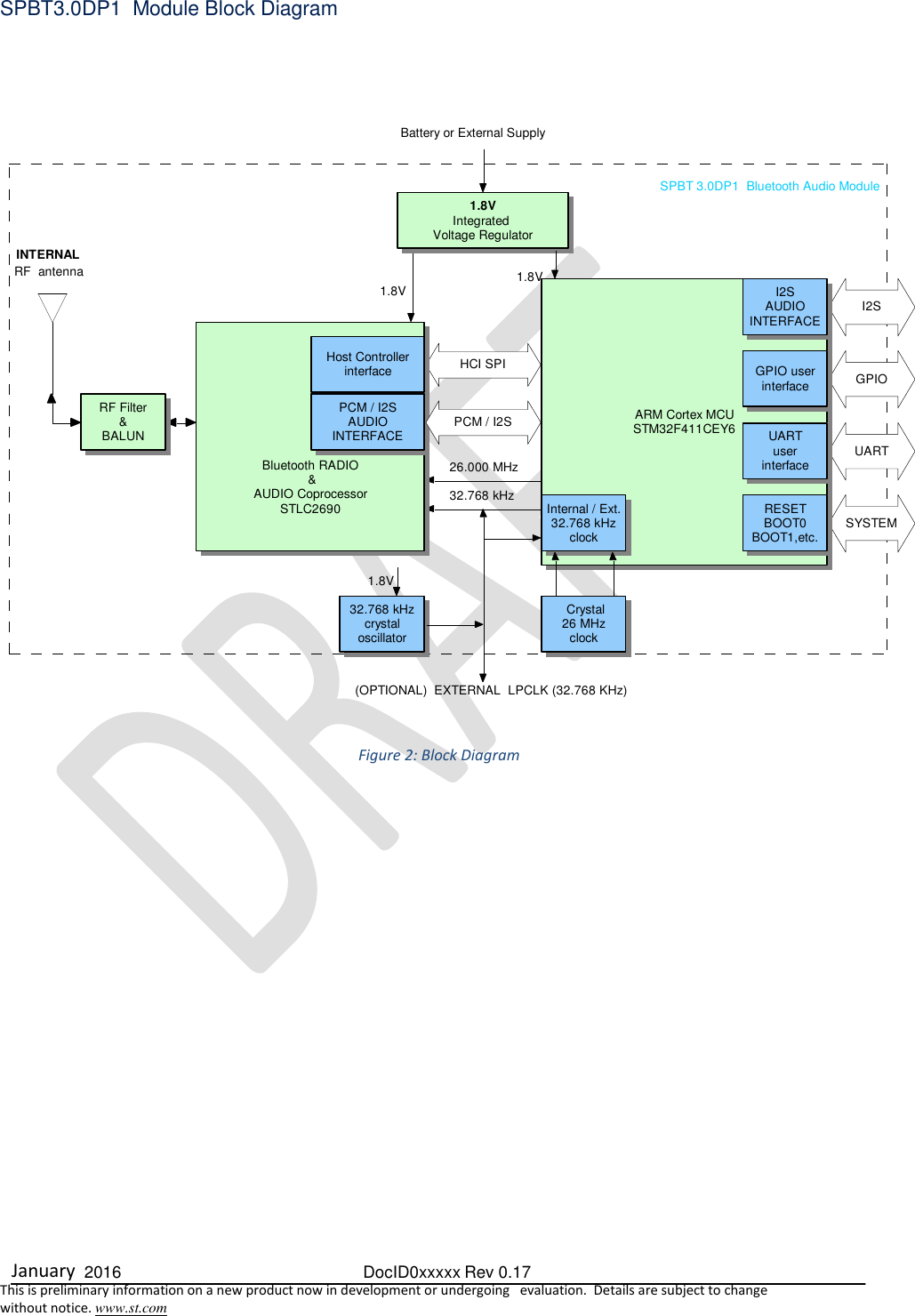
ST Microelectronics S R L SPBT30DP1 SPBT3.0DP1 Bluetooth Module User Manual Bluetooth technology class 2 module
ST Microelectronics S.R.L. SPBT3.0DP1 Bluetooth Module Bluetooth technology class 2 module
UserManual.wiki
>
ST Microelectronics S R L
>
SPBT30DP1 User Manual
Users manual
Navigation menu
Upload a User Manual
Namespaces
Wiki Guide
HTML
PDF
Info
Views
User Manual
Discussion / Help
Navigation
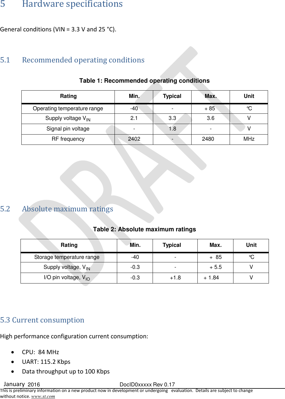
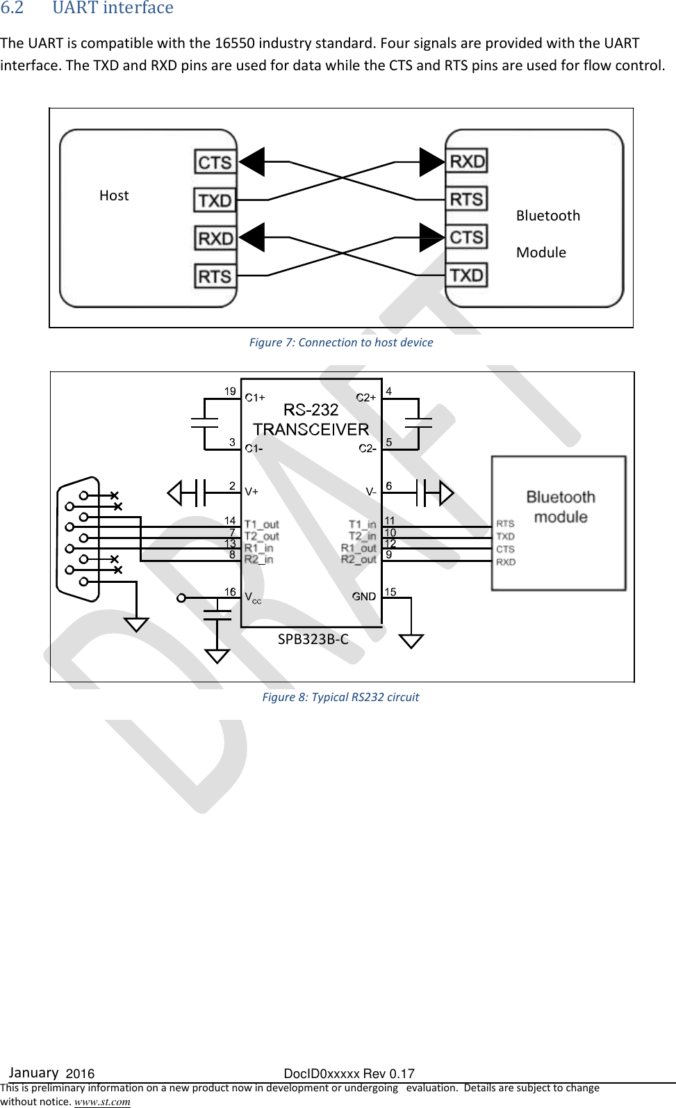
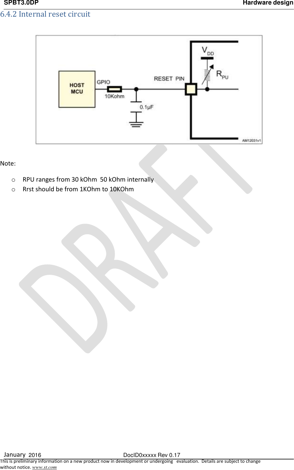
![SPBT3.0DP Hardware design January 2016 DocID0xxxxx Rev 0.17 This is preliminary information on a new product now in development or undergoing evaluation. Details are subject to change without notice. www.st.com 6.3 GPIO interface All GPIOs are capable of sinking and sourcing 4 mA of I/O current. Module GPIO configuration depends on the FW embedded. GPIO1: Bluetooth Connection Status: o 0: BT connection not present o 1: BT connection is present GPIO4: Module Power Status: o 1: module is in Active Mode; o Blinking: module is in Deep Sleep Mode GPIOs can be reconfigured with the following commands o At+ab gpioconfig [GPIO pin] [I/O] o At+ab gpioRead [GPIO pin] o At+ab gpioWrite [GPIO pin] [1/0] For more details refer to the User Manual xxxx. 6.4 Reset circuit Two types of system reset circuits are detailed below. The maximum voltage that can be supplied to the RESET pin is 3.6V. As shown in Figure 10 and Figure 11 the RESET is active low, in absence of a reset circuit the pin is internally pulled up and therefore inactive. 6.4.1 External reset circuit Figure 9: External reset circuit Note: RPU ranges from 30 kOhm to 50 kOhm internally provided ](https://usermanual.wiki/ST-Microelectronics-S-R-L/SPBT30DP1/User-Guide-3028379-Page-16.png)