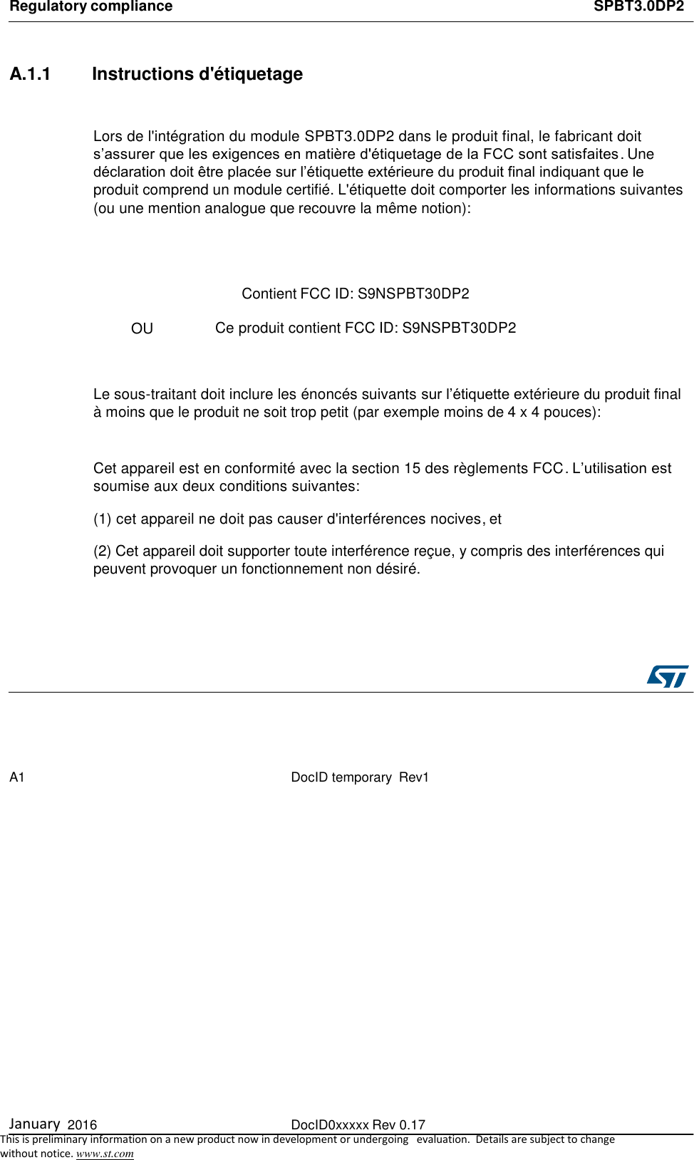
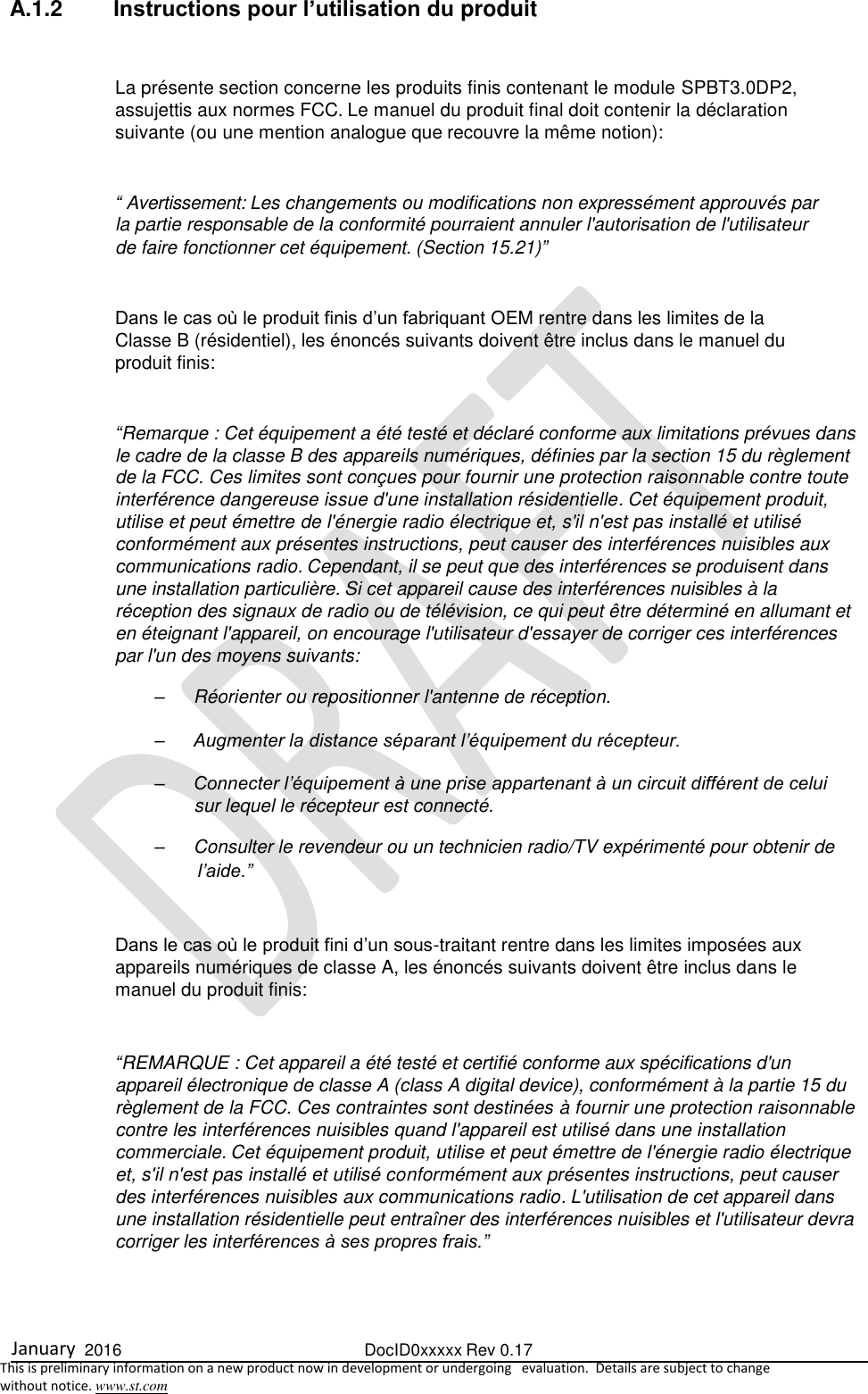
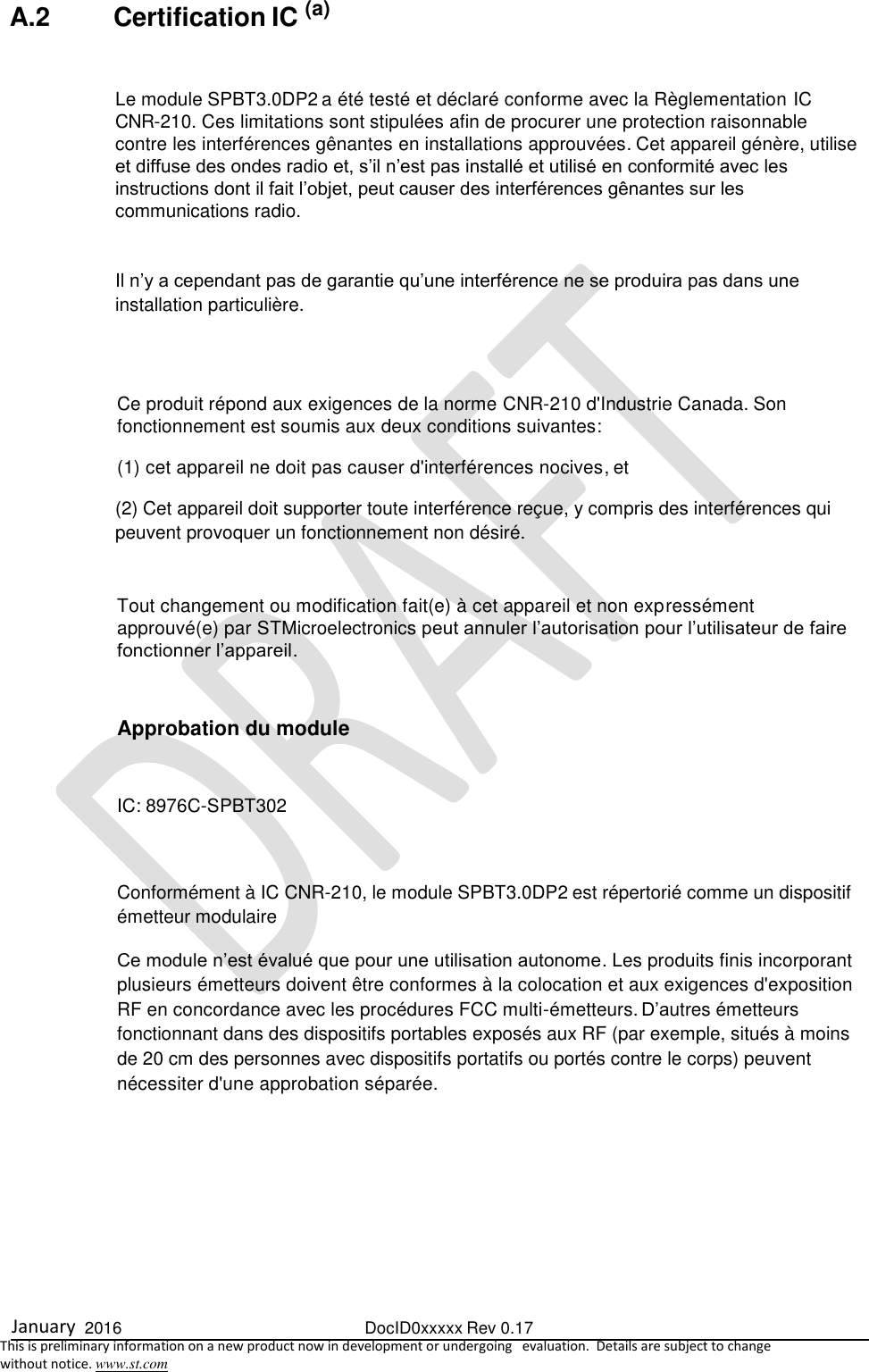
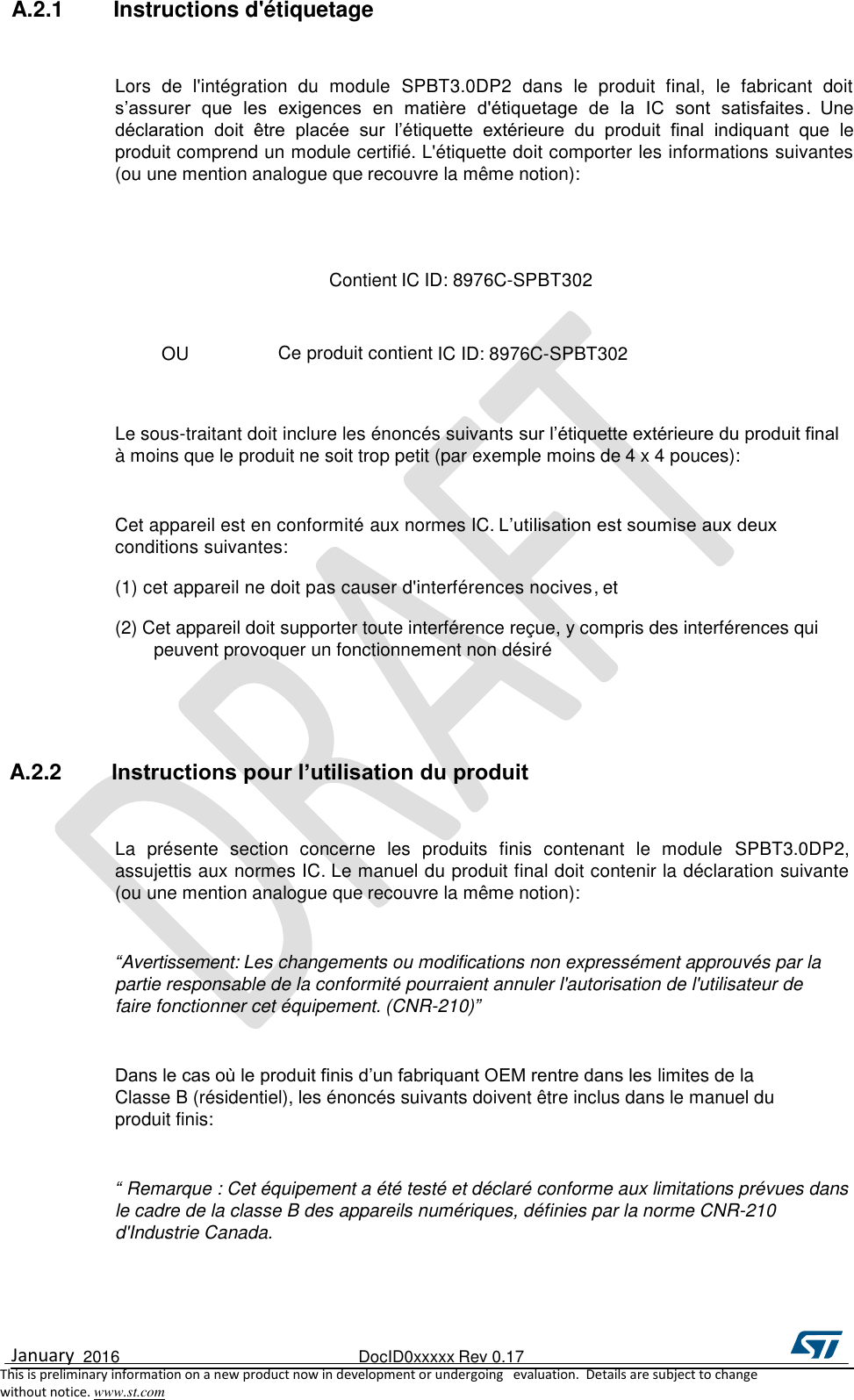
ST Microelectronics S R L SPBT30DP2 SPBT3.0DP2 Bluetooth Module User Manual Bluetooth technology class 2 module

ST Microelectronics S.R.L. SPBT3.0DP2 Bluetooth Module Bluetooth technology class 2 module

Users manual

 January  2016  DocID0xxxxx Rev 0.17   This is preliminary information on a new product now in development or undergoing   evaluation.  Details are subject to change  without notice. www.st.com SPBT3.0DP2    Bluetooth® Classic module    Datasheet – preliminary data  Features  •  Bluetooth® radio o  Fully  embedded  Bluetooth®  v3.0  with SPP and HID profiles o  Embedded support for MFI iAP2 profile o  Class 2 module o  Complete RF ready module o 128-bit encryption security o  Integrated antenna •  ST micro Cortex-M4 microprocessor  o  up to 100 MHz  o 512 KB Flash o  128 KB RAM memory •  Supported transmission speed with SPP o  Up to 800KBits •  General I/O o  8 general purpose I/Os •  User interface o  AT command Data Package (DP) o  Firmware upgrade over UART •  ETSI, FCC, IC and Bluetooth® qualified •  Single voltage supply: 3.3 V typical •  Micro-sized form factor: 11.6 x 13.5 x 2.9 mm •  Operating temperature range: -40 °C to 85 °C
List of tables  January  2016  DocID0xxxxx Rev 0.17   This is preliminary information on a new product now in development or undergoing   evaluation.  Details are subject to change  without notice. www.st.com  Contents 1 Description .......................................................................................................................................... 5 2 RoHS compliance ............................................................................................................................... 6 3 Applications ........................................................................................................................................ 6 4 Software architecture ........................................................................................................................ 7 4.1 BT stack layers ................................................................................................................................ 7 4.2 Supported Profile ........................................................................................................................... 8 4.3 AT Command set: DATA PACKAGE .......................................................................................... 8 5 Hardware specifications ................................................................................................................... 8 5.1 Recommended operating conditions ........................................................................................ 8 5.2 Absolute maximum ratings .......................................................................................................... 8 5.3 High performance current consumption .................................................................................. 9 5.4 Balanced performance current consumption ......................................................................... 9 5.5 Pin assignment ............................................................................................................................. 10 5.6  Mechanical dimensions .............................................................................................................. 11 6 Hardware design ...................................................................................................................................... 13 6.1 Reflow soldering ................................................................................................................................ 13 6.2 UART interface .............................................................................................................................. 15 7 Regulatory compliance ................................................................................................................... 16 7.1 FCC  certification .......................................................................................................................... 16 7.1.1 Labeling instructions ................................................................................................................. 16 7.1.2 Product manual instructions ..................................................................................................... 17 7.2 IC certification .................................................................................................................................. 18 7.2.1 Labeling instructions ................................................................................................................. 18 7.2.2 Product manual instructions ..................................................................................................... 19 7.3 Bluetooth certification ................................................................................................................. 19 7.4 CE certification .............................................................................................................................. 20 8 Traceability ......................................................................................................................................... 21 9 Ordering information ....................................................................................................................... 22 10 Revision history ................................................................................................................................ 23
List of tables  January  2016  DocID0xxxxx Rev 0.17   This is preliminary information on a new product now in development or undergoing   evaluation.  Details are subject to change  without notice. www.st.com    List of tables   Table 1: Recommended operating conditions ................................................................................... 8 Table 2: Absolute maximum ratings ..................................................................................................... 8 Table 3: High Performance Power Consumption .............................................................................. 9 Table 4: Balanced Performance Power Consumption ..................................................................... 9 Table 4: Pin assignment ......................................................................................................................... 10 Table 5: Soldering .................................................................................................................................... 13 Table 6: Traceability information ......................................................................................................... 21 Table 7: Ordering information .............................................................................................................. 22 Table 8: Document revision history .................................................................................................... 23
List of figures  January  2016  DocID0xxxxx Rev 0.17   This is preliminary information on a new product now in development or undergoing   evaluation.  Details are subject to change  without notice. www.st.com  List of figures  Figure 1: Software Architecture Overview .......................................................................................... 7 Figure 2: Pin connection ........................................................................................................................ 10 Figure 3: Mechanical dimensions ........................................................................................................ 11 Figure 4: Recommend land pattern top view .................................................................................... 12 Figure 5: Soldering profile ..................................................................................................................... 14 Figure 6: Connection to host device ................................................................................................... 15 Figure 7: Typical RS232 circuit ............................................................................................................ 15
 January  2016  DocID0xxxxx Rev 0.17   This is preliminary information on a new product now in development or undergoing   evaluation.  Details are subject to change  without notice. www.st.com 1  Description   The SPBT3.0DP2 is an easy to use Bluetooth module, compliant with Bluetooth v3.0.  The module is among the smallest form factor available which provides a complete RF platform. The SPBT3.0DP2 enables electronic devices with wireless connectivity, not requiring any RF experience or expertise for integration into the final product. The SPBT3.0DP2 module, being a certified solution, optimizes the time to market of the final applications.  The module is designed for maximum performance in a minimal space including fast speed UART and 8 general purpose I/O lines, several serial interface options, and up to 800 kbps transmission speed with SPP service active, 250kbps with iAP2 service active.  Optimized design allows the integration of a complete working Bluetooth modem, including antenna, in the minimum possible size;   Deep Sleep Modes allows to reduce power consumption when a Bluetooth connection is not established. Current consumption in Deep Sleep Mode can be reduce even more adding an external LPO (low power oscillator).   The SPBT3.0DP2 is a surface mount PCB module that provides fully embedded, ready to use Bluetooth wireless technology. The reprogrammable Flash memory contains embedded firmware for serial cable replacement using the Bluetooth SPP profile. Embedded Bluetooth DATA PACKAGE (DP) firmware is a friendly interface, which realizes a simple control for cable replacement, enabling communication with most Bluetooth enabled devices, provided that the devices support the SPP profile. The SPBT3.0DP2, supporting iAP2 profile, provides communication with Android, smartphone, and the newest Apple® iOS Bluetooth enabled devices.  An Apple authentication IC is required to exchange data with an Apple device or access an Apple device application. The DP FW includes the Bluetooth iAP2 profile capable of recognizing the Apple authentication chip.  Customers using the Apple authentication IC must register as developers to become an Apple certified MFI member. License fees may apply, for additional information visit: http://developer.apple.com/programs/which-program/index.html.  Certified MFI developers developing electronic accessories that connect to the iPod®, iPhone®, and iPad® gain access to technical documentation, hardware components, technical support and certification logos.  Customized firmware for peripheral device interaction, power optimization, security, and other proprietary features may be supported and can be ordered pre-loaded and configured.
 January  2016  DocID0xxxxx Rev 0.17   This is preliminary information on a new product now in development or undergoing   evaluation.  Details are subject to change  without notice. www.st.com  2  RoHS compliance   ST Bluetooth modules comply with the ECOPACK2 level of RoHS compliance grade.     3  Applications  The SPBT3.0DP2 is suitable for a wide range of application like:  •  Serial cable replacement •  M2M industrial control •  Service diagnostic •  Data acquisition equipment •  Machine control •  Sensor monitoring •  Security system •  Mobile health
 January  2016  DocID0xxxxx Rev 0.17   This is preliminary information on a new product now in development or undergoing   evaluation.  Details are subject to change  without notice. www.st.com  4  Software architecture                                            4.1  BT stack layers  •  Bluetooth v3.0 •  Device power modes: active, deep sleep •  Connection modes: active, sniff •  Wake on Bluetooth feature optimized power consumption of host CPU •  Authentication and encryption •  Encryption key length from 8 bits to 128 bits •  Persistent Flash memory for BD address and user parameter storage •  All ACL (asynchronous connection less) packet types •  Sniff mode: fully supported to maximum allowed intervals  Radio Baseband Link Manager Bluetooth Controller   Bluetooth ProfilesSTM32 Hardware Abstraction Layer Operating System  HCI L2CAP RFCOMM SDP Bluetooth Stack Bluetooth Profiles SPP HID iAP2 STM32F4 controller   Bluetooth ProfilesData Package with AT Command  Application Figure 1: Software Architecture Overview
 January  2016  DocID0xxxxx Rev 0.17   This is preliminary information on a new product now in development or undergoing   evaluation.  Details are subject to change  without notice. www.st.com •  Master slave switch supported during connection and post connection •  Dedicated inquiry access code for improved inquiry scan performance •  Dynamic packet selection channel quality driven data rate to optimize link performance •  Dynamic power control •  Bluetooth radio natively supports 802.11b co-existence AFH •  RFCOMM, SDP, and L2CAP supported   4.2  Supported Profile  •  Serial Port Profile (SPP) •  Human Interface Device (HID) •  iPhone Accessory Profile 2  (iAP2)   4.3  AT Command set: DATA PACKAGE  The complete command list  is reported in the AT Command DATA PACKAGE user manual.   5  Hardware specifications   General conditions (VIN = 3.3 V and 25 °C).   5.1  Recommended operating conditions    Table 1: Recommended operating conditions Rating Min. Typical Max. Unit Operating temperature range -40 -          + 85 °C Supply voltage VIN 2.1 3.3 3.6 V Signal pin voltage - 1.8 - V RF frequency 2402 - 2480 MHz   5.2  Absolute maximum ratings    Table 2: Absolute maximum ratings Rating Min. Typical Max. Unit Storage temperature range -40 - +  85 °C Supply voltage, VIN -0.3 - + 5.5 V I/O pin voltage, VIO -0.3 +1.8   + 1.84 V RF max. input power GFSK - - 10 dBm RF max. input power DQPSK - - 6 dBm RF max. input power DPSK - - -3 dBm
 January  2016  DocID0xxxxx Rev 0.17   This is preliminary information on a new product now in development or undergoing   evaluation.  Details are subject to change  without notice. www.st.com   5.3 High performance current consumption  High performance configuration current consumption:   CPU:  84 MHz    UART: 115.2 Kbps    Data throughput up to 100 Kbps   Temperature: 25 °C  Table 3: High Performance Power Consumption Modes (typical power consumption) Average Unit No connection, Page/Inquiry Scan, no external LPO, Deep Sleep Mode 4.75 mA No connection, Page/Inquiry Scan, with external LPO, Deep Sleep Mode 95 µA No connection, Page/Inquiry Scan, no external LPO, Active Mode 7.9 mA No connection, Page/Inquiry Scan, with external LPO, Active Mode 7.85 mA No connection, No Page/Inquiry Scan, no external LPO, Active Mode 7.65 mA Connection, no data traffic, Master 8.85 mA Connection, no data traffic, Slave 11.45 mA Connection, Master, TX data  17.4 mA Connection, Master, RX data 18.2 mA Connection, Master, TX-RX data  20.8 mA     5.4 Balanced performance current consumption  Balanced performance configuration current consumption:   CPU:  16 MHz    UART: 115.2 Kbps    Data throughput up to 100 Kbps   Temperature: 25 °C   Table 4: Balanced Performance Power Consumption Modes (typical power consumption) Average Unit No connection, Page/Inquiry Scan, no external LPO, Deep Sleep Mode 1.6 mA No connection, Page/Inquiry Scan, with external LPO, Deep Sleep Mode 85 µA No connection, Page/Inquiry Scan, no external LPO, Active Mode 4.1 mA No connection, Page/Inquiry Scan, with external LPO, Active Mode 4.1 mA No connection, No Page/Inquiry Scan, no external LPO, Active Mode 3.9 mA Connection, no data traffic, Master 5.43 mA Connection, no data traffic, Slave 6.95 mA Connection, Master, TX data  14.5 mA Connection, Master, RX data 15.1 mA Connection, Master, TX-RX data  18.3 mA
 January  2016  DocID0xxxxx Rev 0.17   This is preliminary information on a new product now in development or undergoing   evaluation.  Details are subject to change  without notice. www.st.com  5.5  Pin assignment                                   Table 5: Pin assignment Pin Name Description I/O Note 1 GPIO1_BTCS GPIO indicating BT Connection Status -  When high, BT connection is active -  When low, BT connection is not active O  2 GPIO2 General purpose I/O I/O 5V tolerant 3 GPIO3 General purpose I/O I/O 5V tolerant 4 GPIO4_MLPS GPIO indicating Module Low Power Status -  When high, device is in active mode -  When low, device is in low power mode O  5 GPIO5 /  I2C SDA General purpose I/O or I2C_SDA line for MFI chip I/O 5V tolerant 6 GPIO6 / I2C SCL General purpose I/O or I2C_SCL line for MFI chip I/O 5V tolerant 7 GND Reference ground NA  8 Vin Main power supply input  NA  9 Boot 0 Boot 0 pin I 5V tolerant 10 RESETn Reset input (active low for 5ms) I  11 CTS Request to send (active low) I  12 RTS Clear to send (active low) O 5V tolerant 13 RXD Receive Data I 5V tolerant 14 TXD Transmit Data O  15 LPO Low power 32KHz oscillator input I  16 GPIO7 General purpose I/O I/O 5V tolerant 17 GPIO8 General purpose I/O I/O 5V tolerant 18 +1.8V OUT +1.8V out (max 10mA) NA     Figure 2: Pin connection
 January  2016  DocID0xxxxx Rev 0.17   This is preliminary information on a new product now in development or undergoing   evaluation.  Details are subject to change  without notice. www.st.com  5.6   Mechanical dimensions  Figure 3: Mechanical dimensions
 January  2016  DocID0xxxxx Rev 0.17   This is preliminary information on a new product now in development or undergoing   evaluation.  Details are subject to change  without notice. www.st.com Figure 4: Recommend land pattern top view
 January  2016  DocID0xxxxx Rev 0.17   This is preliminary information on a new product now in development or undergoing   evaluation.  Details are subject to change  without notice. www.st.com 6 Hardware design  SPBT3.0DP2 module with DP command embedded FW supports UART, I2C and GPIO hardware interfaces.  Note: -  All unused pins should be left floating; do not ground.  • All GND pins must be well grounded.  • The area around the module should be free of any ground planes, power planes, trace routings, or metal for 6 mm from the module antenna position, in all directions.  • Traces should not be routed underneath the module.   6.1 Reflow soldering  The SPBT3.0DP2 is a high temperature strength surface mount Bluetooth® module supplied on  an  18  pin,  6-layer  PCB.  The  final  assembly  recommended  reflow  profiles  are  indicated here below.  Soldering  phase  must  be  executed  with  care:  in  order  to  avoid  undesired  melting phenomenon, particular attention must be paid to the set-up of the peak temperature.  Here  following  some  suggestions  for  the  temperature  profile  based  on  the  following recommendations.   Table 6: Soldering Profile feature PB-free assembly Average ramp-up rate (TSMAX to TP) 3 °C/sec max Preheat: – Temperature min. (TS min.) – Temperature max. (TS max.) – Time (ts min. to ts max.)(ts)  150 °C 200 °C 60-100 sec Time maintained above: – Temperature TL – Temperature TL  217 °C 60-70 sec Peak temperature (TP) 240 + 0 °C Time within 5 °C of actual peak temperature (TP) 10-20 sec Ramp-down rate 6 °C/sec Time from 25 °C to peak temperature 8 minutes max.
 January  2016  DocID0xxxxx Rev 0.17   This is preliminary information on a new product now in development or undergoing   evaluation.  Details are subject to change  without notice. www.st.com                            $012026Y1                                     Figure 5: Soldering profile
 January  2016  DocID0xxxxx Rev 0.17   This is preliminary information on a new product now in development or undergoing   evaluation.  Details are subject to change  without notice. www.st.com  6.2  UART interface  The UART is compatible with the 16550 industry standard. Four signals are provided with the UART interface. The TXD and RXD pins are used for data while the CTS and RTS pins are used for flow control.          Host Bluetooth module      $012027Y1                        $012028Y1                   Figure 6: Connection to host device Figure 7: Typical RS232 circuit
 January  2016  DocID0xxxxx Rev 0.17   This is preliminary information on a new product now in development or undergoing   evaluation.  Details are subject to change  without notice. www.st.com  7  Regulatory compliance   7.1  FCC  certification  This module has been tested and found to comply with the FCC part 15 rules. These limits are designed to provide reasonable protection against harmful interference in approved installations. This equipment generates, uses, and can radiate radio frequency energy and, if not installed and used in accordance with the instructions, may cause harmful interference to radio communications.  However, there is no guarantee that interference may not occur in a particular installation.  This device complies with part 15 of the FCC rules. Operation is subject to the following two conditions:  1  This device may not cause harmful interference,  and  2  this device must accept any interference received, including interference that may cause undesired operation.  Modifications or changes to this equipment not expressly approved by STMicroelectronics may render void the user's authority to operate this equipment.  The safe user distance, for RF Exposure, is ≥ 5mm (in compliance with 447498 D01 General RF Exposure Guidance v06). Modular approval  FCC ID: S9NSPBT30DP2  In accordance with FCC part 15, the SPBT3.0DP2 is listed as a modular transmitter device.  This module is evaluated for stand-alone use only. Finished products incorporating multiple transmitters must comply with colocation and RF exposure requirements in accordance with FCC multi-transmitter product procedures. Collocated transmitters operating in portable RF Exposure conditions (e.g. <20 cm from persons including but not limited to body worn and hand held devices) may require separate approval.  7.1.1 Labeling instructions  When integrating the SPBT3.0DP2 into the final product, the OEM must ensure that the FCC labeling requirements are satisfied. A statement must be included on the exterior of the final product which indicates the product includes a certified module. The label should state the following (or similar wording that conveys the same meaning):  Contains FCC ID: S9NSPBT30DP2  OR  This product contains FCC ID: S9NSPBT30DP2  The OEM must include the following statements on the exterior of the final product unless the product is too small (e.g. less than 4 x 4 inches)This device complies with Part 15 of the FCC Rules. Operation is subject to the following two conditions:  1  this device may not cause harmful interference, and  2  this device must accept any interference received, including any interference that may cause undesired operation.
 January  2016  DocID0xxxxx Rev 0.17   This is preliminary information on a new product now in development or undergoing   evaluation.  Details are subject to change  without notice. www.st.com 7.1.2 Product manual instructions  This section applies to OEM final products containing the SPBT3.0DP2 module, subject to FCC compliance. The final product manual must contain the following statement (or a similar statement that conveys the same meaning):  Warning: Changes or modifications not expressly approved by the party responsible for compliance could void the user's authority to operate the equipment. (Part. 15.21)  In the case where an OEM seeks Class B (residential) limits for the final product, the following statement must be included in the final product manual:  Note:       This equipment has been tested and found to comply with the limits for a Class B digital device, pursuant to part 15 of the FCC Rules. These limits are designed to provide reasonable protection against harmful interference in a residential installation. This equipment generates, uses and can radiate radio frequency energy and, if not installed and used in accordance with the instructions, may cause harmful interference to radio communications. However, there is no guarantee that interference will not occur in a particular installation. If this equipment does cause harmful interference to radio or television reception, which can be determined by turning the equipment off and on, the user is encouraged to try to correct the interference by one or more of the following measures:  •  Reorient or relocate the receiving antenna.  •  Increase the separation between the equipment and receiver.  •  Connect the equipment into an outlet on a circuit different from that to which the receiver is connected.  •  Consult the dealer or an experienced radio/TV technician for help.   In the case where an OEM seeks the lesser category of a Class A digital device for the final product, the following statement must be included in the final product manual:  Note:       This equipment has been tested and found to comply with the limits for a Class A digital device, pursuant to part 15 of the FCC Rules. These limits are designed to provide reasonable protection against harmful interference when the equipment is operated in a commercial environment. This equipment generates, uses, and can radiate radio frequency energy and, if not installed and used in accordance with the instruction manual, may cause harmful interference to radio communications. Operation of this equipment in a residential area is likely to cause harmful interference in which case the user will be required to correct the interference at his expense.
 January  2016  DocID0xxxxx Rev 0.17   This is preliminary information on a new product now in development or undergoing   evaluation.  Details are subject to change  without notice. www.st.com  7.2 IC certification  The SPBT3.0DP2 module has been tested and found compliant with the IC RSS-247 rules. These limits are designed to provide reasonable protection against harmful interference in approved installations. This equipment generates, uses, and can radiate radio frequency energy and, if not installed and used in accordance with the instructions, may cause harmful interference to radio communications.  However, there is no guarantee that interference may not occur in a particular installation.  This device complies with RSS-247 of the IC rules. Operation is subject to the following two conditions:  1  this device may not cause harmful interference, and  2  this device must accept any interference received, including interference that may cause undesired operation.   Modifications or changes to this equipment not expressly approved by STMicroelectronics may render void the user's authority to operate this equipment.  The safe user distance, for RF Exposure, is ≥ 15mm (in compliance with RSS-102 Issue 5). Modular approval  IC: 8976C-SPBT302 In accordance with IC RSS-247, the SPBT3.0DP2 is listed as a modular transmitter device.  This module is evaluated for stand-alone use only. Finished products incorporating multiple transmitters must comply with colocation and RF exposure requirements in accordance with IC multi-transmitter product procedures. Collocated transmitters operating in portable RF Exposure conditions (e.g. <20cm from persons including but not limited to body worn and hand held devices) may require separate approval.    7.2.1 Labeling instructions  When integrating the SPBT3.0DP2 into the final product, the OEM must ensure that the IC labeling requirements are satisfied. A statement must be included on the exterior of the final product which indicates that the product includes a certified module. The label should state the following (or similar wording that conveys the same meaning):  Contains IC: 8976C-SPBT302 OR This product contains IC: 8976C-SPBT302  The OEM must include the following statements on the exterior of the final product unless the product is too small (e.g. less than 4 x 4 inches):  This device complies with RSS-247 of the IC Rules. Operation is subject to the following two conditions:  1  this device may not cause harmful interference, and  2  this device must accept any interference received, including any interference that may cause undesired operation.
 January  2016  DocID0xxxxx Rev 0.17   This is preliminary information on a new product now in development or undergoing   evaluation.  Details are subject to change  without notice. www.st.com  7.2.2 Product manual instructions  This section applies to OEM final products containing the SPBT3.0DP2 module, subject to IC compliance. The final product manual must contain the following statement (or a similar statement that conveys the same meaning):  Warning: Changes or modifications not expressly approved by the party responsible for compliance could void the user's authority to operate the equipment. (RSS-247)  In the case where an OEM seeks Class B (residential) limits for the final product, the following statement must be included in the final product manual:  Note:       This equipment has been tested and found to comply with the limits for a Class B digital device, pursuant to RSS-247 of the IC Rules. These limits are designed to provide reasonable protection against harmful interference in a residential installation. This equipment generates, uses and can radiate radio frequency energy and, if not installed and used in accordance with the instructions, may cause harmful interference to radio communications. However, there is no guarantee that interference will not occur in a particular installation. If this equipment does cause harmful interference to radio or television reception, which can be determined by turning the equipment off and on, the user is encouraged to try to correct the interference by one or more of the following measures:  •  Reorient or relocate the receiving antenna.  • Increase the separation between the equipment and receiver.  •  Connect the equipment into an outlet on a circuit different from that to which the receiver is connected.  •  Consult the dealer or an experienced radio/TV technician for help.   In the case where an OEM seeks the lesser category of a Class A digital device for the final product, the following statement must be included in the final product manual:  Note:       This equipment has been tested and found to comply with the limits for a Class A digital device, pursuant to RSS-247 of the IC Rules. These limits are designed to provide reasonable protection against harmful interference when the equipment is operated in a commercial environment. This equipment generates, uses, and can radiate radio frequency energy and, if not installed and used in accordance with the instruction manual, may cause harmful interference to radio communications. Operation of this equipment in a residential area is likely to cause harmful interference in which case the user will be required to correct the interference at his expense.          7.3 Bluetooth certification  Module with embedded stack and profile has been qualified according to SIG qualification
 January  2016  DocID0xxxxx Rev 0.17   This is preliminary information on a new product now in development or undergoing   evaluation.  Details are subject to change  without notice. www.st.com rules: –  Bluetooth SIG Declaration ID: zzzzzz –  Product type: End Product –  Core spec version: 3.0 –  Product descriptions: Bluetooth module, spec V3.0   7.4  CE certification  Module has been certified according to following certification rules: – CE Expert opinion: vvvvvv – Measurements have been performed in accordance with (report available on request): –  EN 300 328  –  EN 301 489 -–  EN 301 489  -–  EN60950- CE certified:                   (See the A.1 at the bottom of this document for the French translation)
 January  2016  DocID0xxxxx Rev 0.17   This is preliminary information on a new product now in development or undergoing   evaluation.  Details are subject to change  without notice. www.st.com  8 Traceability   Each module is univocally identified by serial number stored in a 2D data matrix laser marked on the bottom side of the module itself.  The serial number has the following format:  WW YY D FF NNN    Table 7: Traceability information Letter Meaning  WW week YY year D Product ID number FF Production panel coordinate identification  NN Progressive serial number    Each module bulk is identified by a bulk ID. BULK ID and module 2D data matrix are linked by a reciprocal traceability link. The module 2D data matrix traces the lot number of any raw material used.
 January  2016  DocID0xxxxx Rev 0.17   This is preliminary information on a new product now in development or undergoing   evaluation.  Details are subject to change  without notice. www.st.com 9  Ordering information      Table 8: Ordering information Order code Description Packing MOQ SPBT3.0DP2 Class 2 OEM Bluetooth antenna module Jedec tray 2448 pcs
Regulatory compliance SPBT3.0DP2   January  2016  DocID0xxxxx Rev 0.17   This is preliminary information on a new product now in development or undergoing   evaluation.  Details are subject to change  without notice. www.st.com  10  Revision history   Table 9: Document revision history Date Revision Changes  07- July - 2015 0.14 First release 31 – July - 2015 0.15 Fixed typo (CTS,RTS) in table 3 08 - January - 2016 0.16 Added FW Architecture picture, Power Consumption tables 08 - January - 2016 0.17 Updated to SPBT3.0DP2
Regulatory compliance SPBT3.0DP2   January  2016  DocID0xxxxx Rev 0.17   This is preliminary information on a new product now in development or undergoing   evaluation.  Details are subject to change  without notice. www.st.com   Déclaration de conformité   A.1  Certification FCC   Le module SPBT3.0DP2 a été testé et déclaré conforme avec la section 15 de la Règlementation FCC. Ces limitations sont stipulées afin de procurer une protection raisonnable contre les interférences gênantes dans les installations approuvées. Cet appareil génère, utilise et diffuse des ondes radio et, s’il n’est pas installé et utilisé en conformité avec les instructions dont il fait l’objet, peut causer des interférences gênantes sur les communications radio.   Il n’y a cependant pas de garantie qu’une interférence ne se produira pas dans une installation particulière.  Cet appareil est en conformité avec la section 15 des règlements FCC. L’utilisation est soumise aux deux conditions suivantes: (1) cet appareil ne doit pas causer d'interférences nocives, et (2) Cet appareil doit supporter toute interférence reçue, y compris des interférences qui peuvent provoquer un fonctionnement non désiré.  Tout changement ou modification fait(e) à cet appareil et non expressément approuvé(e) par STMicroelectronics peut annuler l’autorisation pour l’utilisateur de faire fonctionner l’appareil.  Approbation du module  FCC ID: S9NSPBT30DP2  Conformément à la section 15 des règlements FCC, le module SPBT3.0DP2 est répertorié comme un dispositif émetteur modulaire.   Ce module n’est évalué que pour une utilisation autonome. Les produits finis incorporant plusieurs émetteurs doivent être conformes à la colocation et aux exigences d'exposition  RF en concordance avec les procédures FCC multi-émetteurs. D’autres émetteurs fonctionnant dans des dispositifs portables exposés aux RF (par exemple, situés à moins de 20 cm des personnes avec dispositifs portatifs ou portés contre le corps) peuvent nécessiter d'une approbation séparée.
Regulatory compliance SPBT3.0DP2   January  2016  DocID0xxxxx Rev 0.17   This is preliminary information on a new product now in development or undergoing   evaluation.  Details are subject to change  without notice. www.st.com  A.1.1  Instructions d'étiquetage  Lors de l'intégration du module SPBT3.0DP2 dans le produit final, le fabricant doit s’assurer que les exigences en matière d'étiquetage de la FCC sont satisfaites . Une déclaration doit être placée sur l’étiquette extérieure du produit final indiquant que le produit comprend un module certifié. L'étiquette doit comporter les informations suivantes (ou une mention analogue que recouvre la même notion):   Contient FCC ID: S9NSPBT30DP2 OU Ce produit contient FCC ID: S9NSPBT30DP2  Le sous-traitant doit inclure les énoncés suivants sur l’étiquette extérieure du produit final à moins que le produit ne soit trop petit (par exemple moins de 4 x 4 pouces):  Cet appareil est en conformité avec la section 15 des règlements FCC. L’utilisation est soumise aux deux conditions suivantes:  (1) cet appareil ne doit pas causer d'interférences nocives, et  (2) Cet appareil doit supporter toute interférence reçue, y compris des interférences qui peuvent provoquer un fonctionnement non désiré.       A1  DocID temporary  Rev1
 January  2016  DocID0xxxxx Rev 0.17   This is preliminary information on a new product now in development or undergoing   evaluation.  Details are subject to change  without notice. www.st.com  A.1.2  Instructions pour l’utilisation du produit  La présente section concerne les produits finis contenant le module SPBT3.0DP2, assujettis aux normes FCC. Le manuel du produit final doit contenir la déclaration suivante (ou une mention analogue que recouvre la même notion):  “ Avertissement: Les changements ou modifications non expressément approuvés par la partie responsable de la conformité pourraient annuler l'autorisation de l'utilisateur de faire fonctionner cet équipement. (Section 15.21)”  Dans le cas où le produit finis d’un fabriquant OEM rentre dans les limites de la Classe B (résidentiel), les énoncés suivants doivent être inclus dans le manuel du produit finis:  “Remarque : Cet équipement a été testé et déclaré conforme aux limitations prévues dans le cadre de la classe B des appareils numériques, définies par la section 15 du règlement de la FCC. Ces limites sont conçues pour fournir une protection raisonnable contre toute interférence dangereuse issue d'une installation résidentielle. Cet équipement produit, utilise et peut émettre de l'énergie radio électrique et, s'il n'est pas installé et utilisé conformément aux présentes instructions, peut causer des interférences nuisibles aux communications radio. Cependant, il se peut que des interférences se produisent dans une installation particulière. Si cet appareil cause des interférences nuisibles à la réception des signaux de radio ou de télévision, ce qui peut être déterminé en allumant et en éteignant l'appareil, on encourage l'utilisateur d'essayer de corriger ces interférences par l'un des moyens suivants: –  Réorienter ou repositionner l'antenne de réception. – Augmenter la distance séparant l’équipement du récepteur. – Connecter l’équipement à une prise appartenant à un circuit différent de celui sur lequel le récepteur est connecté. –  Consulter le revendeur ou un technicien radio/TV expérimenté pour obtenir de l’aide.”  Dans le cas où le produit fini d’un sous-traitant rentre dans les limites imposées aux appareils numériques de classe A, les énoncés suivants doivent être inclus dans le manuel du produit finis:  “REMARQUE : Cet appareil a été testé et certifié conforme aux spécifications d'un appareil électronique de classe A (class A digital device), conformément à la partie 15 du règlement de la FCC. Ces contraintes sont destinées à fournir une protection raisonnable contre les interférences nuisibles quand l'appareil est utilisé dans une installation commerciale. Cet équipement produit, utilise et peut émettre de l'énergie radio électrique et, s'il n'est pas installé et utilisé conformément aux présentes instructions, peut causer des interférences nuisibles aux communications radio. L'utilisation de cet appareil dans une installation résidentielle peut entraîner des interférences nuisibles et l'utilisateur devra corriger les interférences à ses propres frais.”
 January  2016  DocID0xxxxx Rev 0.17   This is preliminary information on a new product now in development or undergoing   evaluation.  Details are subject to change  without notice. www.st.com  A.2  Certification IC (a)  Le module SPBT3.0DP2 a été testé et déclaré conforme avec la Règlementation IC CNR-210. Ces limitations sont stipulées afin de procurer une protection raisonnable contre les interférences gênantes en installations approuvées. Cet appareil génère, utilise et diffuse des ondes radio et, s’il n’est pas installé et utilisé en conformité avec les instructions dont il fait l’objet, peut causer des interférences gênantes sur les communications radio.  Il n’y a cependant pas de garantie qu’une interférence ne se produira pas dans une installation particulière.    Ce produit répond aux exigences de la norme CNR-210 d'Industrie Canada. Son fonctionnement est soumis aux deux conditions suivantes:  (1) cet appareil ne doit pas causer d'interférences nocives, et  (2) Cet appareil doit supporter toute interférence reçue, y compris des interférences qui peuvent provoquer un fonctionnement non désiré.  Tout changement ou modification fait(e) à cet appareil et non expressément approuvé(e) par STMicroelectronics peut annuler l’autorisation pour l’utilisateur de faire fonctionner l’appareil.  Approbation du module  IC: 8976C-SPBT302  Conformément à IC CNR-210, le module SPBT3.0DP2 est répertorié comme un dispositif émetteur modulaire  Ce module n’est évalué que pour une utilisation autonome. Les produits finis incorporant plusieurs émetteurs doivent être conformes à la colocation et aux exigences d'exposition  RF en concordance avec les procédures FCC multi-émetteurs. D’autres émetteurs fonctionnant dans des dispositifs portables exposés aux RF (par exemple, situés à moins de 20 cm des personnes avec dispositifs portatifs ou portés contre le corps) peuvent nécessiter d'une approbation séparée.
 January  2016  DocID0xxxxx Rev 0.17   This is preliminary information on a new product now in development or undergoing   evaluation.  Details are subject to change  without notice. www.st.com A.2.1  Instructions d'étiquetage  Lors  de  l'intégration  du  module  SPBT3.0DP2  dans  le  produit  final,  le  fabricant  doit s’assurer  que  les  exigences  en  matière  d'étiquetage  de  la  IC  sont  satisfaites .  Une déclaration  doit  être  placée  sur  l’étiquette  extérieure  du  produit  final  indiquant  que  le produit comprend un module certifié. L'étiquette doit comporter les informations suivantes (ou une mention analogue que recouvre la même notion):   Contient IC ID: 8976C-SPBT302  OU Ce produit contient IC ID: 8976C-SPBT302  Le sous-traitant doit inclure les énoncés suivants sur l’étiquette extérieure du produit final à moins que le produit ne soit trop petit (par exemple moins de 4 x 4 pouces):  Cet appareil est en conformité aux normes IC. L’utilisation est soumise aux deux conditions suivantes:  (1) cet appareil ne doit pas causer d'interférences nocives, et  (2) Cet appareil doit supporter toute interférence reçue, y compris des interférences qui peuvent provoquer un fonctionnement non désiré   A.2.2  Instructions pour l’utilisation du produit  La  présente  section  concerne  les  produits  finis  contenant  le  module  SPBT3.0DP2, assujettis aux normes IC. Le manuel du produit final doit contenir la déclaration suivante (ou une mention analogue que recouvre la même notion):  “Avertissement: Les changements ou modifications non expressément approuvés par la partie responsable de la conformité pourraient annuler l'autorisation de l'utilisateur de faire fonctionner cet équipement. (CNR-210)”  Dans le cas où le produit finis d’un fabriquant OEM rentre dans les limites de la Classe B (résidentiel), les énoncés suivants doivent être inclus dans le manuel du produit finis:  “ Remarque : Cet équipement a été testé et déclaré conforme aux limitations prévues dans le cadre de la classe B des appareils numériques, définies par la norme CNR-210 d'Industrie Canada.
 January  2016  DocID0xxxxx Rev 0.17   This is preliminary information on a new product now in development or undergoing   evaluation.  Details are subject to change  without notice. www.st.com Ces limites sont conçues pour fournir une protection raisonnable contre toute interférence dangereuse issue d'une installation résidentielle. Cet équipement produit, utilise et peut émettre de l'énergie radio électrique et, s'il n'est pas installé et utilisé conformément aux présentes instructions, peut causer des interférences nuisibles aux communications radio. Cependant, il se peut que des interférences se produisent dans une installation particulière. Si cet appareil cause des interférences nuisibles à la réception des signaux de radio ou de télévision, ce qui peut être déterminé en allumant et en éteignant l'appareil, nous encourageons l'utilisateur à essayer de corriger ces interférences par l'un des moyens suivants: –  Réorienter ou repositionner l'antenne de réception. – Augmenter la distance séparant l’équipement du récepteur. – Connecter l’équipement à une prise appartenant à un circuit différent de celui sur lequel le récepteur est connecté. –  Consulter le revendeur ou un technicien radio/TV expérimenté pour obtenir de l’aide.”  Dans le cas où le produit finis d’un fabriquant OEM rentre dans le cadre des limites imposées aux appareils numériques de classe A, les énoncés suivants doivent être inclus dans le manuel du produit finis:  “ REMARQUE: Cet appareil a été testé et certifié conforme aux spécifications d'un appareil électronique de classe A (class A digital device), conformément à la norme CNR-210 d'Industrie Canada. Ces contraintes sont destinées à fournir une protection raisonnable contre les interférences nuisibles quand l'appareil est utilisé dans une installation commerciale. Cet équipement produit, utilise et peut émettre de l'énergie radio électrique et, s'il n'est pas installé et utilisé conformément aux présentes instructions, peut causer des interférences nuisibles aux communications radio. L'utilisation de cet appareil dans une installation résidentielle peut entraîner des interférences nuisibles et l'utilisateur devra corriger les interférences à ses propres frais.”              A.3  Certification CE
 January  2016  DocID0xxxxx Rev 0.17   This is preliminary information on a new product now in development or undergoing   evaluation.  Details are subject to change  without notice. www.st.com Le module SPBT3.0DP2 a obtenu une certification de conformité aux normes suivantes: –  EN 300 328  V1.8.1 :2012 –  EN 300 328  V1.9.1 :2015 –  EN 301 489-17 V2.2.1 :2009 –  EN 301 489-1 V1.9.2:2011 –  EN 62479 :2010 –  EN60950-1:2006 + A11:2009 + A1:2010 + A12:2011 + A2 :2013  Le module est certifié CE:
 January  2016  DocID0xxxxx Rev 0.17   This is preliminary information on a new product now in development or undergoing   evaluation.  Details are subject to change  without notice. www.st.com                        IMPORTANT NOTICE  - PLEASE READ CAREFULLY:    STMicroelectronics NV and its subsidiaries (“ST”) reserve the right to make changes, corrections, enhancements, modifications, and improvements to ST products and/or to this document at any time without notice. Purchasers should obtain the latest relevant information on ST products before placing orders. ST products are sold pursuant to ST’s terms and conditions of sale in place at the time of order acknowledgement  Purchasers are solely responsible for the choice, selection, and use of ST products and ST assumes no liability for application assistance or the design of Purchasers’ products   No license, express or implied, to any intellectual property rights is granted by ST herein.   Resale of ST products with provisions different from the information set forth herein shall void any warranty granted by ST for such product.   ST and the ST logo are trademarks of ST. All other product or service names are the property of their respective owners.   Information in this document supersedes and replaces information previously supplied in any prior versions of this document.   © 2015 STMicroelectronics - All rights reserved    www.st.com

Navigation menu