ST Microelectronics S R L SPBT40DP SPBT4.0DP Bluetooth Dual Radio Module User Manual SPBT40DP Datasheet r0 15 Rizzoli
ST Microelectronics S.R.L. SPBT4.0DP Bluetooth Dual Radio Module SPBT40DP Datasheet r0 15 Rizzoli
Datasheet
July
2015 DocID0xxxxx Rev 0.15
This is preliminary information on a new product now in development or undergoing evaluation. Details are subject to change
without notice. www.st.com
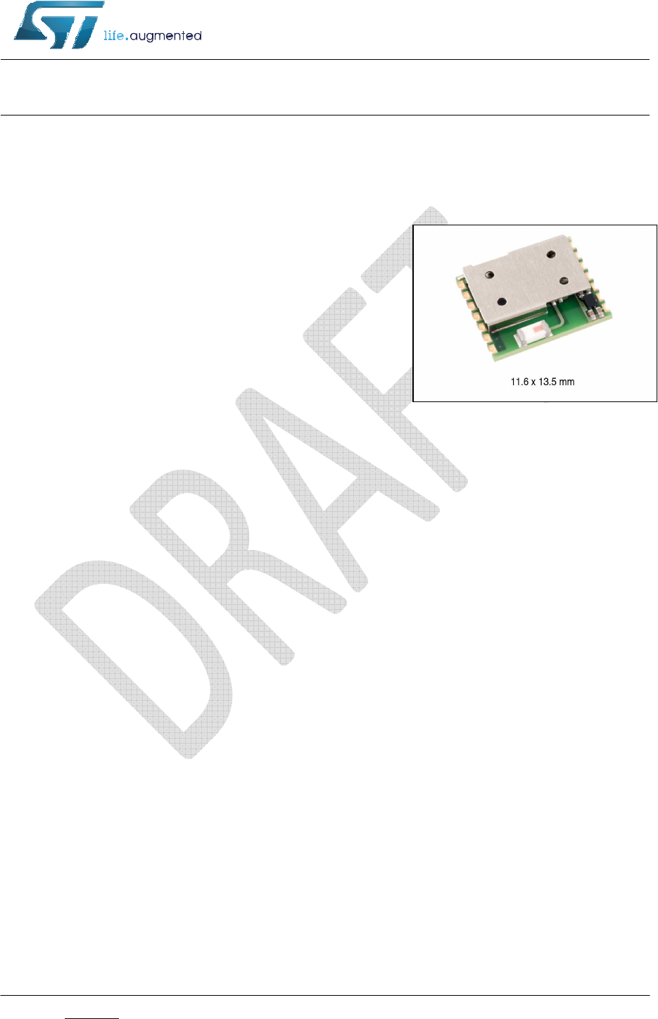
SPBT4.0DP
Bluetooth® Smart Ready
module
Datasheet – preliminary data
Features
•
•
Bluetooth® radio
o Fully embedded Bluetooth® v4.0
with SPP and Low Energy profiles
o Embedded support for MFI iAP2 profile
o Class 2 module
o Complete RF ready module
o 128-bit encryption security
o Integrated antenna
• ST micro Cortex-M4 microprocessor
o up to 104 MHz
o 512 KB Flash
o 128 KB RAM memory
• Supported transmission speed with SPP
o Up to 800KBits
• General I/O
o 8 general purpose I/Os
• User interface
o AT command Data Package (DP)
o Firmware upgrade over UART
• ETSI, FCC, IC and Bluetooth® qualified
• Single voltage supply: 3.3 V typical
• Micro-sized form factor: 11.6 x 13.5 x 2.9 mm
• Operating temperature range: -40 °C to 85 °C

Contents
1 Description .......................................................................................................................... 5
2 RoHS compliance ................................................................................................................ 6
3 Applications ......................................................................................................................... 6
4 Software architecture .......................................................................................................... 7
4.1 BT stack layers ................................................................................................................. 7
4.2 Supported Profile ............................................................................................................. 7
4.3 AT Command DATA PACKAGE ....................................................................................... 7
5 Hardware specifications...................................................................................................... 8
5.1 Recommended operating conditions .............................................................................. 8
5.2 Absolute maximum ratings .............................................................................................. 8
5.3 Modulei current absorption ............................................................................................. 8
5.4 Pin assignment ................................................................................................................. 9
5.5 Mechanical dimensions ................................................................................................. 10
6 Hardware design .................................................................................................................... 12
6.1 Reflow soldering ............................................................................................................. 12
6.2 UART interface ............................................................................................................... 14
7 Regulatory compliance ..................................................................................................... 15
7.1 FCC certification ............................................................................................................ 15
7.1.1 Labeling instructions ............................................................................................... 15
7.1.2 Product manual instructions ................................................................................... 16
7.2 IC certification ................................................................................................................. 17
7.2.1 Labeling instructions ............................................................................................... 17
7.2.2 Product manual instructions ................................................................................... 18
7.3 Bluetooth certification .................................................................................................... 19
7.4 CE certification ............................................................................................................... 19
8
Traceability
......................................................................................................................... 20
9 Ordering information ......................................................................................................... 21
10 Revision history ................................................................................................................. 22

List
of
tables
3 | P a g e
List of tables
Table 1. Recommended operating conditions . . . . . . . . . . . . . . . . . . . . . . . . . . . . . . . . . . . . . . . . . 8
Table 2. Absolute maximum ratings . . . . . . . . . . . . . . . . . . . . . . . . . . . . . . . . . . . . . . . . . . . . . . . . . 8
Table 3. Pin
assignment
. . . . . . . . . . . . . . . . . . . . . . . . . . . . . . . . . . . . . . . . . . . . . . . . . . . . . . . . . . 9
Table 4. Soldering . . . . . . . . . . . . . . . . . . . . . . . . . . . . . . . . . . . . . . . . . . . . . . . . . . . . . . . . . . . . . .12
Table 5. Traceability information. . . . . . . . . . . . . . . . . . . . . . . . . . . . . . . . . . . . . . . . . . . . . . . . . . . 20
Table 6. Ordering
information
. . . . . . . . . . . . . . . . . . . . . . . . . . . . . . . . . . . . . . . . . . . . . . . . . . . . . . 21
Table 7. Document revision history . . . . . . . . . . . . . . . . . . . . . . . . . . . . . . . . . . . . . . . . . . . . . . . . . 22

List
of
figu
r
es
4 | P a g e
List of figures
Figure 1. Pin connection . . . . . . . . . . . . . . . . . . . . . . . . . . . . . . . . . . . . . . . . . . . . . . . . . . . . . . . . . . 9
Figure 2. Mechanical dimensions . . . . . . . . . . . . . . . . . . . . . . . . . . . . . . . . . . . . . . . . . . . . . . . . . . . 10
Figure 3. Recommend land pattern top view . . . . . . . . . . . . . . . . . . . . . . . . . . . . . . . . . . . . . . . . . . 11
Figure 4. Soldering profile . . . . . . . . . . . . . . . . . . . . . . . . . . . . . . . . . . . . . . . . . . . . . . . . . . . . . . . . . 13
Figure 5. Connection to host device . . . . . . . . . . . . . . . . . . . . . . . . . . . . . . . . . . . . . . . . . . . . . . . . . 14
Figure 6. Typical RS232 circuit . . . . . . . . . . . . . . . . . . . . . . . . . . . . . . . . . . . . . . . . . . . . . . . . . . . . . 14

5 | P a g e
1 Description
The SPBT4.0DP is an easy to use Bluetooth Smart Ready module, compliant with Bluetooth
v4.0.
The module is among the smallest form factor available which provides a complete RF
platform. The SPBT4.0DP enables electronic devices with wireless connectivity, not
requiring any RF experience or expertise for integration into the final product. The
SPBT4.0DP module, being a certified solution, optimizes the time to market of the final
applications.
The module is designed for maximum performance in a minimal space including fast speed
UART and 8 general purpose I/O lines, several serial interface options, and up to 800 kbps
transmission speed with SPP service active, 250kbps with iAP2 service active.
Optimized design allows the integration of a complete working Bluetooth modem, including
antenna, in the minimum possible size; only an additional external LPO (low power
oscillator) is required to enable low power mode capability.
The SPBT4.0DP is a surface mount PCB module that provides fully embedded, ready to
use Bluetooth wireless technology. The reprogrammable Flash memory contains
embedded firmware for serial cable replacement using the Bluetooth SPP profile.
Embedded Bluetooth DATA PACKAGE (DP) firmware is a friendly interface, which realizes a
simple control for cable replacement. The SPBT4.0DP supporting SPP, iAP2 and Bluetooth
Low Energy proprietary Data Exchange profiles, it provides communication with Android,
smartphone, and the newest Apple
®
iOS Bluetooth enabled devices.
An Apple authentication IC is required to exchange data with an Apple device or access an
Apple device application. The DP FW includes the Bluetooth iAP2 profile capable of
recognizing the Apple authentication chip.
Customers using the Apple authentication IC must register as developers to become an
Apple certified MFI member. License fees may apply, for additional information visit:
http://developer.apple.com/programs/which-program/index.html.
Certified MFI developers developing electronic accessories that connect to the iPod
®
,
iPhone
®
, and iPad
®
gain access to technical documentation, hardware components,
technical support and certification logos.
Customized firmware for peripheral device interaction, power optimization, security, and
other proprietary features may be supported and can be ordered pre-loaded and configured.

6 | P a g e
2 RoHS compliance
ST Bluetooth modules comply with the ECOPACK2 level of RoHS compliance grade.
3 Applications
The SPBT4.0DP is suitable for a wide range of application like:
•
Serial cable replacement
•
M2M industrial control
•
Service diagnostic
•
Data acquisition equipment
•
Machine control
•
Sensor monitoring
•
Security system
•
Mobile health

7 | P a g e
4 Software architecture
4.1 BT stack layers
•
Bluetooth v4.0
•
Device power modes: active, sleep and deep sleep
•
Wake on Bluetooth feature optimized power consumption of host CPU
•
Authentication and encryption
•
Encryption key length from 8 bits to 128 bits
•
Persistent Flash memory for BD address and user parameter storage
•
All ACL (asynchronous connection less) packet types
•
Sniff mode: fully supported to maximum allowed intervals
•
Master slave switch supported during connection and post connection
•
Dedicated inquiry access code for improved inquiry scan performance
•
Dynamic packet selection channel quality driven data rate to optimize link performance
•
Dynamic power control
•
Bluetooth radio natively supports 802.11b co-existence AFH
•
RFCOMM, SDP, and L2CAP supported
4.2 Supported Profile
Bluetooth Classic:
• Serial Port Profile (SPP)
• iPOD Accessory Protocol 2 (iAP2)
Bluetooth Low Energy:
•
Proprietary Data Exchange Profile (DEP)
4.3 AT Command DATA PACKAGE
The complete command list is reported in the AT Command DATA PACKAGE user manual.

8 | P a g e
5 Hardware specifications
General conditions (V
IN
= 3.3 V and 25
°C).
5.1 Recommended operating conditions
Table 1. Recommended operating conditions
Rating
Min.
Typical
Max.
Unit
Operating temperature range
-40
-
+ 85
°C
Supply voltage
V
IN
2.3
3.3
3.6
V
Signal pin voltage
-
2.1
-
V
RF frequency
2402
-
2480
MHz
5.2 Absolute maximum ratings
Table 2. Absolute maximum ratings
Rating
Min.
Typical
Max.
Unit
Storage temperature range
-40
-
+ 85
°C
Supply voltage,
V
IN
-0.3
-
+
5.5
V
I/O pin voltage,
V
IO
-0.3
+2.1 +5
V
RF max. input power GFSK
-
-
10
dBm
RF max. input power DQPSK
-
-
6
dBm
RF max. input power DPSK
-
-
-3
dBm
5.3 Module current absorption (Average & Typical)
Table 3. Module average D.C. current absorption
Test Conditions
Min.
Typical
Max.
Unit
CPU = 84Mhz
IDLE STATE
(WAIT FOR COMMANDS)
10.62
mA
CPU = 84Mhz
Tx (65500kb/s)
Transmission state
(Continuos Transmission)
37
mA
CPU = 84Mhz
Rx (35500kb/s)
Receiving state
27
mA
9 | P a g e
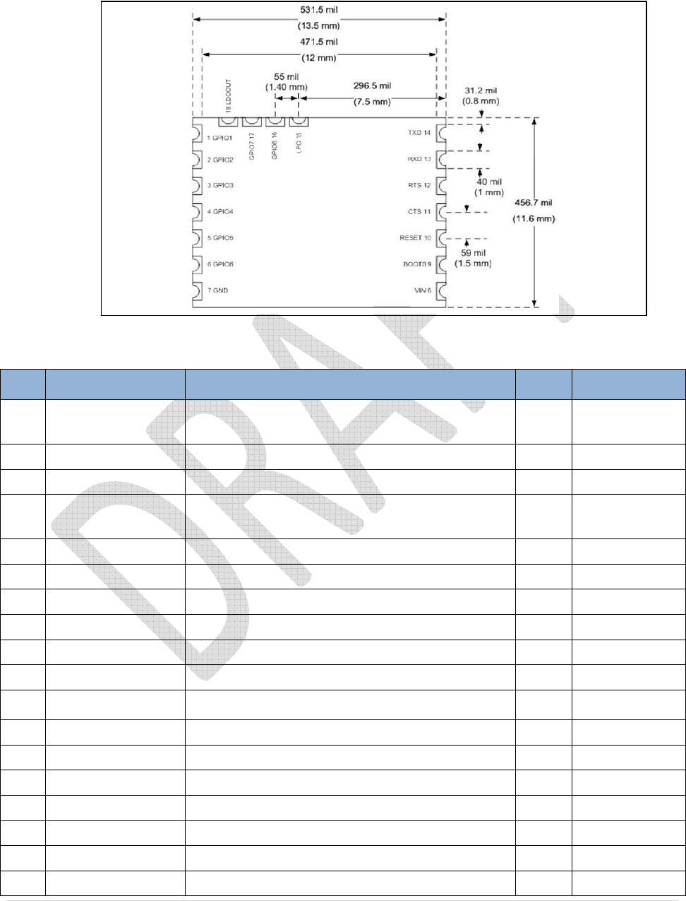
5.4 Pin assignment
Figure 1. Pin connection
Table 4. Pin
assignment
Pin Name Description I/O Note
1 GPIO1_BTCS GPIO indicating BT Connection Status
- When high, BT connection is active
- When low, BT connection is not active
O
2 GPIO2 General purpose I/O I/O 5V tolerant
3 GPIO3 General purpose I/O I/O 5V tolerant
4 GPIO4_MLPS GPIO indicating Module Low Power Status
- When high, device is in active mode
- When low, device is in low power mode
O
5 GPIO5 General purpose I/O I/O 5V tolerant
6 GPIO6 General purpose I/O I/O 5V tolerant
7 GND Reference ground NA
8 Vin Main power supply input NA
9 Boot 0 Boot 0 pin I 5V tolerant
10 RESETn Reset input (active low for 5ms) I
11 CTS / I2C SCL Request to send (active low) or I2C_SCL line for MFI
chip I
12 RTS / I2C SDA Clear to send (active low) or I2C_SDA line for MFI chip O 5V tolerant
13 RXD Receive Data I 5V tolerant
14 TXD Transmit Data O
15 LPO Low power 32KHz oscillator input I
16 GPIO7 General purpose I/O I/O 5V tolerant
17 GPIO8 General purpose I/O I/O 5V tolerant
18 +2.1V OUT +2.1V out (max 10mA) NA
10 | P a g e
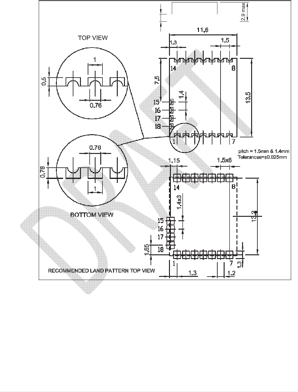
5.5 Mechanical dimensions
Figure 2. Mechanical dimensions
11 | P a g e
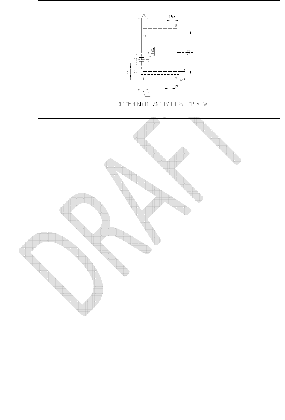
Figure 3. Recommend land pattern top view
12 | P a g e
6 Hardware design
SPBT4.0DP module with DP command embedded FW supports UART, I
2
C and GPIO
hardware interfaces.
Note: - All unused pins should be left floating; do not ground.
• All GND pins must be well grounded.
• The area around the module should be free of any ground planes, power planes, trace
routings, or metal for 6 mm from the module antenna position, in all directions.
• Traces should not be routed underneath the module.
6.1 Reflow soldering
The SPBT4.0DP is a high temperature strength surface mount Bluetooth
®
module supplied on
an 18 pin, 6-layer PCB. The final assembly recommended reflow profiles are indicated here
below.
Soldering phase must be executed with care: in order to avoid undesired melting
phenomenon, particular attention must be paid to the set-up of the peak temperature.
Here following some suggestions for the temperature profile based on the following
recommendations.
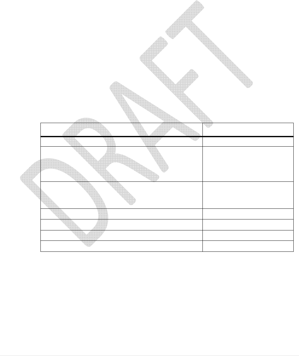
Table 5.
Soldering
Profile
feature
PB-free assembly
Average ramp-up rate (T
SMAX
to
T
P
)
3 °C/sec max
Preheat:
– Temperature min. (T
S
min.)
– Temperature max. (T
S
max.)
– Time (t
s
min. to t
s
max.)(t
s
)
150
°C
200
°C
60-100
sec
Time maintained above:
– Temperature
T
L
– Temperature
T
L
217
°C
60-70
sec
Peak temperature (T
P
) 240 + 0
°C
Time within 5 °C of actual peak temperature (T
P
) 10-20
sec
Ramp-down rate 6
°C/sec
Time from 25 °C to peak temperature 8 minutes max.
13 | P a g e
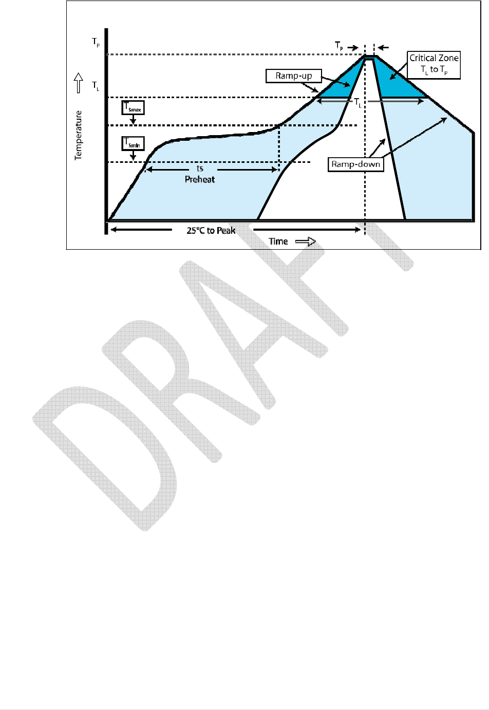
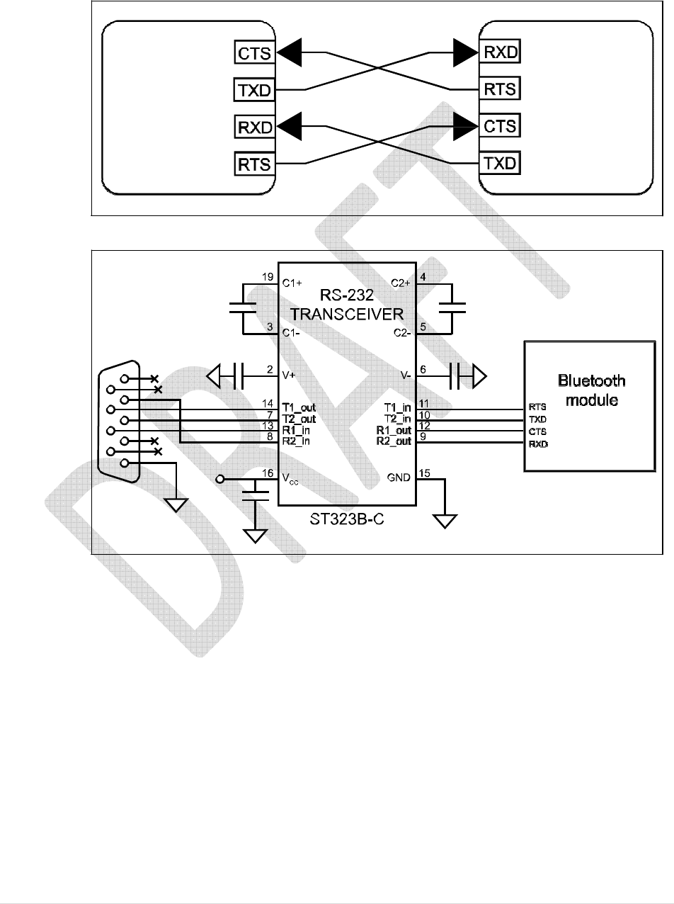
Figure 4. Soldering profile
$012026Y1
14 | P a g e
6.2 UART interface
The UART is compatible with the 16550 industry standard. Four signals are provided with
the UART interface. The TXD and RXD pins are used for data while the CTS and RTS pins
are used for flow control.
Figure 5. Connection to host device
Host
Bluetooth
module
$012027Y1
Figure 6. Typical RS232 circuit
$012028Y1

15 | P a g e
7 Regulatory compliance
7.1 FCC certification
This module has been tested and found to comply with the FCC part 15 rules. These limits are
designed to provide reasonable protection against harmful interference in approved
installations. This equipment generates, uses, and can radiate radio frequency energy and, if
not installed and used in accordance with the instructions, may cause harmful interference to
radio communications.
However, there is no guarantee that interference may not occur in a particular installation.
This device complies with part 15 of the FCC rules. Operation is subject to the following two
conditions:
1 This device may not cause harmful interference,
and
2 this device must accept any interference received, including interference that may cause
undesired operation.
Modifications or changes to this equipment not expressly approved by STMicroelectronics
may render void the user's authority to operate this equipment.
Modular approval
FCC ID: S9NSPBT40DP
In accordance with FCC part 15, the SPBT4.0DP is listed as a modular transmitter device.
This module is evaluated for stand-alone use only. Finished products incorporating multiple
transmitters must comply with colocation and RF exposure requirements in accordance with
FCC multi-transmitter product procedures. Collocated transmitters operating in portable RF
Exposure conditions (e.g. <20 cm from persons including but not limited to body worn and
hand held devices) may require separate approval.
7.1.1 Labeling instructions
When integrating the SPBT4.0DP into the final product, the OEM must ensure that the FCC
labeling requirements are satisfied. A statement must be included on the exterior of the final
product which indicates the product includes a certified module. The label should state the
following (or similar wording that conveys the same meaning):
Contains FCC ID: S9NSPBT40DP
OR
This product contains FCC ID: S9NSPBT40DP
The OEM must include the following statements on the exterior of the final product unless
the product is too small (e.g. less than 4 x 4 inches)This device complies with Part 15 of the
FCC Rules. Operation is subject to the following two conditions:
1 this device may not cause harmful interference, and
2 this device must accept any interference received, including any interference that may
cause undesired operation.

16 | P a g e
7.1.2 Product manual instructions
This section applies to OEM final products containing the SPBT4.0DP module, subject to
FCC compliance. The final product manual must contain the following statement (or a similar
statement that conveys the same meaning):
Warning: Changes or modifications not expressly approved by the party responsible for
compliance could void the user's authority to operate the equipment. (Part. 15.21)
In the case where an OEM seeks Class B (residential) limits for the final product, the
following statement must be included in the final product manual:
Note: This equipment has been tested and found to comply with the limits for a Class B digital device,
pursuant to part 15 of the FCC Rules. These limits are designed to provide reasonable
protection against harmful interference in a residential installation. This equipment generates,
uses and can radiate radio frequency energy and, if not installed and used in accordance with
the instructions, may cause harmful interference to radio communications. However, there is
no guarantee that interference will not occur in a particular installation. If this equipment does
cause harmful interference to radio or television reception, which can be determined by
turning the equipment off and on, the user is encouraged to try to correct the interference by
one or more of the following measures:
• Reorient or relocate the receiving antenna.
• Increase the separation between the equipment and receiver.
• Connect the equipment into an outlet on a circuit different from that to which the receiver is
connected.
• Consult the dealer or an experienced radio/TV technician for help.
In the case where an OEM seeks the lesser category of a Class A digital device for the final
product, the following statement must be included in the final product manual:
Note: This equipment has been tested and found to comply with the limits for a Class A digital device,
pursuant to part 15 of the FCC Rules. These limits are designed to provide reasonable
protection against harmful interference when the equipment is operated in a commercial
environment. This equipment generates, uses, and can radiate radio frequency energy and, if
not installed and used in accordance with the instruction manual, may cause harmful
interference to radio communications. Operation of this equipment in a residential area is
likely to cause harmful interference in which case the user will be required to correct the
interference at his expense.

17 | P a g e
7.2 IC certification
The SPBT4.0DP module has been tested and found compliant with the IC RSS-210 rules.
These limits are designed to provide reasonable protection against harmful interference in
approved installations. This equipment generates, uses, and can radiate radio frequency
energy and, if not installed and used in accordance with the instructions, may cause harmful
interference to radio communications.
However, there is no guarantee that interference may not occur in a particular installation.
This device complies with RSS-210 of the IC rules. Operation is subject to the following two
conditions:
1 this device may not cause harmful interference, and
2 this device must accept any interference received, including interference that may cause
undesired operation.
Modifications or changes to this equipment not expressly approved by STMicroelectronics
may render void the user's authority to operate this equipment.
Modular approval
IC: 8976C-SPBT40DP
In accordance with IC RSS-210, the SPBT4.0DP is listed as a modular transmitter device.
This module is evaluated for stand-alone use only. Finished products incorporating multiple
transmitters must comply with colocation and RF exposure requirements in accordance with
IC multi-transmitter product procedures. Collocated transmitters operating in portable RF
Exposure conditions (e.g. <20cm from persons including but not limited to body worn and
hand held devices) may require separate approval.
7.2.1 Labeling instructions
When integrating the SPBT4.0DP into the final product, the OEM must ensure that the IC
labeling requirements are satisfied. A statement must be included on the exterior of the final
product which indicates that the product includes a certified module. The label should state
the following (or similar wording that conveys the same meaning):
Contains IC: 8976C-SPBT40DP OR This product contains IC: 8976C-SPBT40DP
The OEM must include the following statements on the exterior of the final product unless
the product is too small (e.g. less than 4 x 4 inches):
This device complies with RSS-210 of the IC Rules. Operation is subject to the following two
conditions:
1 this device may not cause harmful interference, and
2 this device must accept any interference received, including any interference that may
cause undesired operation.

18 | P a g e
7.2.2 Product manual instructions
This section applies to OEM final products containing the SPBT4.0DP module, subject to IC
compliance. The final product manual must contain the following statement (or a similar
statement that conveys the same meaning):
Warning: Changes or modifications not expressly approved by the party responsible for
compliance could void the user's authority to operate the equipment. (RSS-210)
In the case where an OEM seeks Class B (residential) limits for the final product, the
following statement must be included in the final product manual:
Note: This equipment has been tested and found to comply with the limits for a Class B digital device,
pursuant to RSS-210 of the IC Rules. These limits are designed to provide reasonable
protection against harmful interference in a residential installation. This equipment generates,
uses and can radiate radio frequency energy and, if not installed and used in accordance with
the instructions, may cause harmful interference to radio communications. However, there is
no guarantee that interference will not occur in a particular installation. If this equipment does
cause harmful interference to radio or television reception, which can be determined by
turning the equipment off and on, the user is encouraged to try to correct the interference by
one or more of the following measures:
• Reorient or relocate the receiving antenna.
• Increase the separation between the equipment and receiver.
• Connect the equipment into an outlet on a circuit different from that to which the receiver is
connected.
• Consult the dealer or an experienced radio/TV technician for help.
In the case where an OEM seeks the lesser category of a Class A digital device for the final
product, the following statement must be included in the final product manual:
Note: This equipment has been tested and found to comply with the limits for a Class A digital device,
pursuant to RSS-210 of the IC Rules. These limits are designed to provide reasonable
protection against harmful interference when the equipment is operated in a commercial
environment. This equipment generates, uses, and can radiate radio frequency energy and, if
not installed and used in accordance with the instruction manual, may cause harmful
interference to radio communications. Operation of this equipment in a residential area is
likely to cause harmful interference in which case the user will be required to correct the
interference at his expense.
19 | P a g e
7.3 Bluetooth certification
Module with embedded stack and profile has been qualified according to SIG qualification
rules:
– Bluetooth SIG Declaration ID: zzzzzz
– Product type: End Product
– Core spec version: 4.0
– Product descriptions: Bluetooth module, spec V4.0
7.4 CE certification
Module has been certified according to following certification rules:
– CE Expert opinion: 0564-ARSP00100
– Measurements have been performed in accordance with (report available on
request):
– EN 300 328 v 1.8.1 (2012-06) ; v1.9.1 (2015-02)
– EN 301 489-17 V 2.2.1 (2012-09)
-– EN 62479 (2010-09)
-– EN60950- 1:2006 + A11:2009 + A1:2010 + A12:2011 + A2:2013
CE certified:

20 | P a g e
8
Traceability
Each module is univocally identified by serial number stored in a 2D data matrix laser
marked on the bottom side of the module itself.
The serial number has the following format: WW YY D FF NNN
Table 5. Traceability information
Letter Meaning
WW week
YY year
D Product ID number
FF Production panel coordinate identification
NN Progressive serial number
Each module bulk is identified by a bulk ID.
BULK ID and module 2D data matrix are linked by a reciprocal traceability link.
The module 2D data matrix traces the lot number of any raw material used.

21 | P a g e
9 Ordering information
Table 6. Ordering information
Order code
Description
Packing
MOQ
SPBT4.0DP Class 2 OEM Bluetooth antenna module
Jedec tray 2448 pcs

22 | P a g e
10 Revision history
Table 7. Document revision history
Date
Revision
Changes
07-July- 2015
0.14
First release.
31 – July - 2015
0.15
Modified table 3

23 | P a g e
IMPORTANT NOTICE - PLEASE READ CAREFULLY:
STMicroelectronics NV and its subsidiaries (“ST”) reserve the right to make changes, corrections, enhancements, modifications, and
improvements to ST products and/or to this document at any time without notice. Purchasers should obtain the latest relevant information
on
ST products before placing orders. ST products are sold pursuant to ST’s terms and conditions of sale in place at the time of order
acknowledgement
Purchasers are solely responsible for the choice, selection, and use of ST products and ST assumes no liability for application assistance or
the design of Purchasers’ products
No license, express or implied, to any intellectual property rights is granted by ST herein.
Resale of ST products with provisions different from the information set forth herein shall void any warranty granted by ST for such product.
ST and the ST logo are trademarks of ST. All other product or service names are the property of their respective owner
s.
Information in this document supersedes and replaces information previously supplied in any prior versions of this document.
© 2015 STMicroelectronics - All rights
reserved
www.st.com