ST Microelectronics S R L SPSGRF SPSGRF-915 series / SubGiga Module User Manual SPSGRF 868 or 915 Datasheet 2014 12 18
ST Microelectronics S.R.L. SPSGRF-915 series / SubGiga Module SPSGRF 868 or 915 Datasheet 2014 12 18
UserManual.wiki
>
ST Microelectronics S R L
>
SPSGRF User Manual
User Manual
Navigation menu
Upload a User Manual
Namespaces
Wiki Guide
HTML
PDF
Info
Views
User Manual
Discussion / Help
Navigation
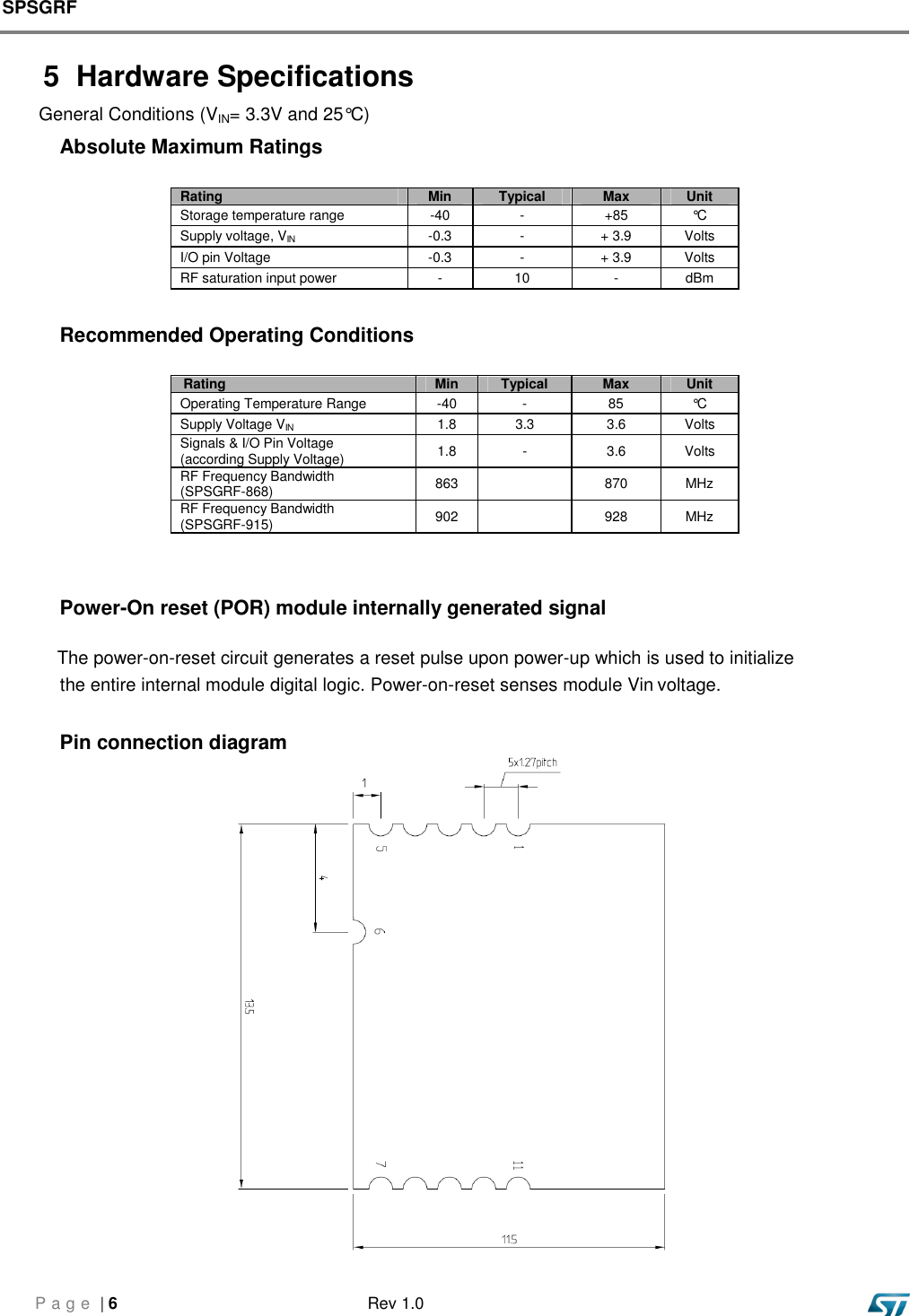
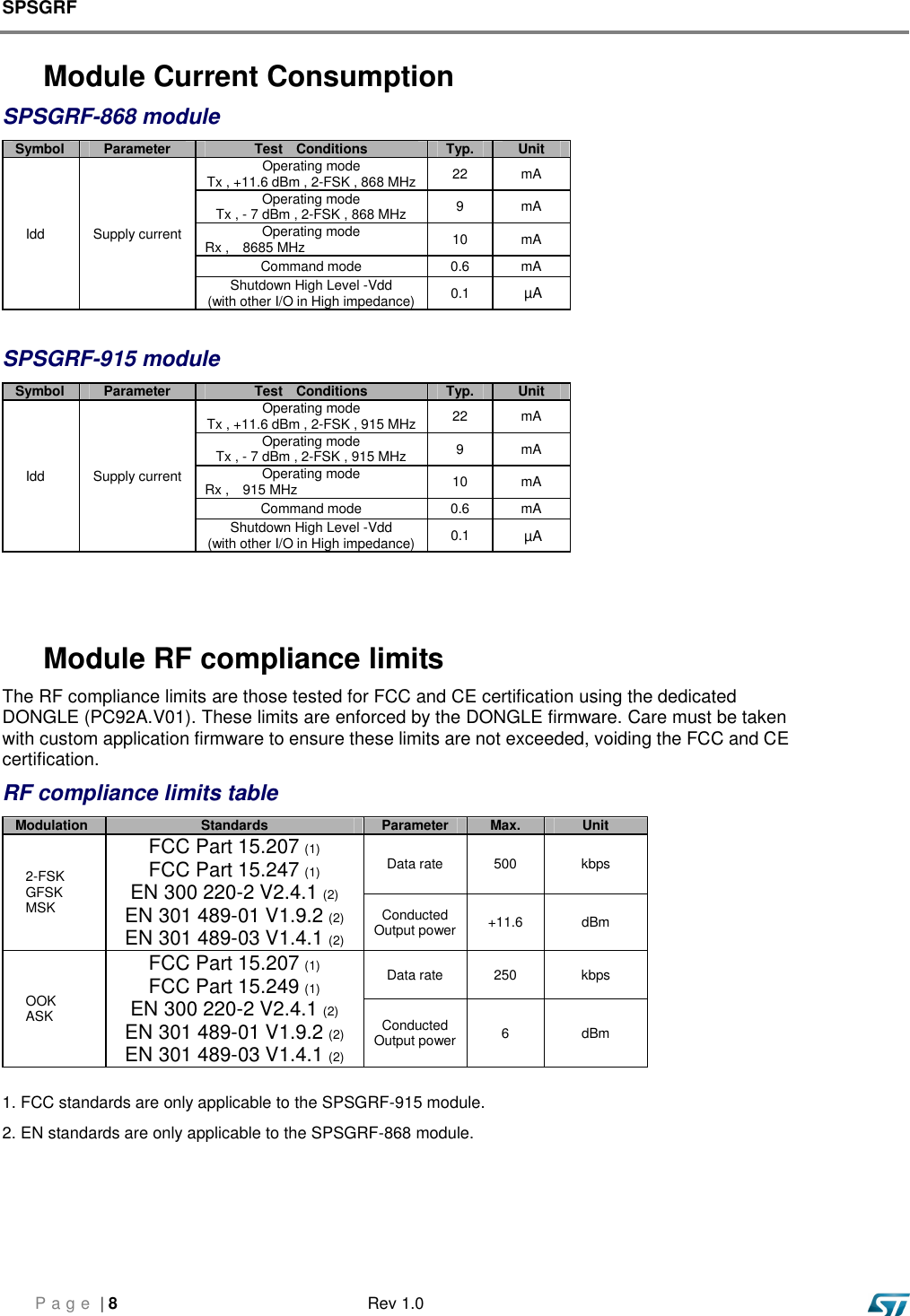
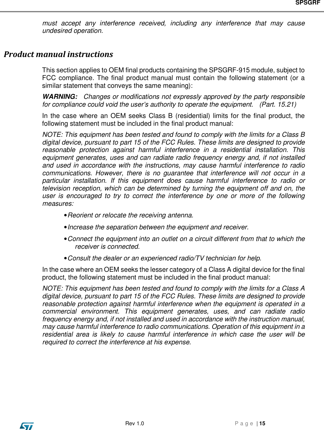
![SPSGRF Rev 1.0 P a g e | 7 Pin Assignment Name Type Pin # Description ALT Function V max. Tolerant Initial State SPI Interface SPI_CLK I 7 SPI CLOCK (Max. 8 MHz) Vin SPI_MOSI I 9 SPI MOSI (MASTER out SLAVE in) Vin SPI_MISO O 8 SPI MISO (MASTER in / SLAVE out) Vin SPI_CS I 10 SPI “Chip Select” (SPI slave select) Vin Power and Ground Vin 5 Vin (1.8V + 3.6V max.) GND 6 GND Module SHUTDOWN SDN I 11 SHUTDOWN input (active high.) (1.8V + Vin max). GPIO – General Purpose Input/Output GPIO [0] I/O 4 Programmable Input / Output & Analog Temperature output (1.8V + Vin max.). Digital Output. Low Power GPIO [1] I/O 3 Programmable Input / Output (1.8V + Vin max.). Digital Output. Low Power GPIO [2] I/O 2 Programmable Input / Output (1.8V + Vin max.). Digital Output. Low Power GPIO [3] I/O 1 Programmable Input / Output (1.8V + Vin max.). Digital Output. Low Power Pin1 = GPIO_3 (TBD) Pin11 = SDN Pin2 = GPIO_2 (TBD) Pin10 = SPI_CS Pin3 = GPIO_1 (TBD) Pin9 = SPI_MOSI Pin4 = GPIO_0 (TBD) Pin8 = SPI_MISO Pin5 = Vin Pin7 = SPI_CLK Pin6 = GND](https://usermanual.wiki/ST-Microelectronics-S-R-L/SPSGRF/User-Guide-2523193-Page-4.png)