ST Microelectronics S R L SPSGRF SPSGRF-915 series / SubGiga Module User Manual SPSGRF 868 or 915 Datasheet 2014 12 18
ST Microelectronics S.R.L. SPSGRF-915 series / SubGiga Module SPSGRF 868 or 915 Datasheet 2014 12 18
User Manual

SPSGRF-868 / 915
SubGiga (868 or 915 MHz) programmable
transceiver module
Datasheet
April 2014 rev 0.1
This is preliminary information on a new product now in development or undergoing evaluation. Details are subject
to change without notice. www.st.com
www.st.com
Features
• Programmable Radio features
- Modulation schemes: 2-FSK, GFSK,
MSK, GMSK, OOk, ASK
- Air data rate from 1 to 500 kbps
- On board antenna
• RF features
- Receiver sensitivity: -118 dBm
- Programmable RF output power
• Host Interface
- SPI
• General I/O
- Up to 32 programmable I/O functions on
4 GPIO programmable module pins
• Two Carrier Frequency versions
- 868 MHz tuned antenna (Europe)
- 915 MHz tuned antenna (USA)
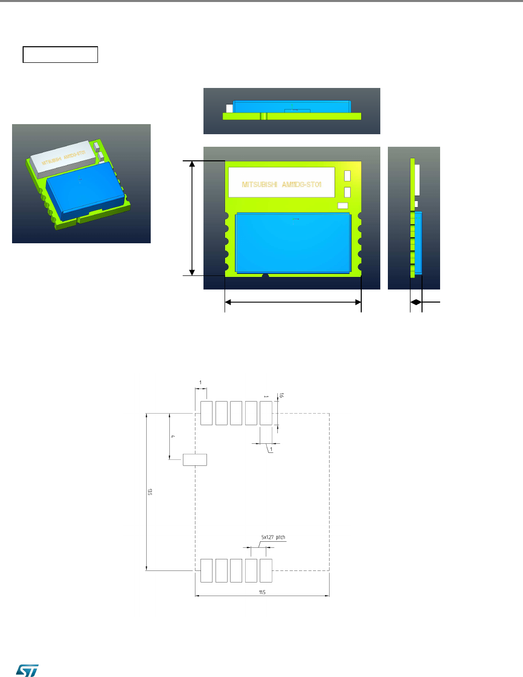
Preliminary module picture
11.5 mm x 13.5 mm x 2.0 mm

SPSGRF
P a g e | 2 Rev 1.0
1 Description
The SPSGRF is an easy to use sub-gigahertz transceiver module, with many programmable
features. The module provides a complete RF platform in a tiny form factor.
The SPSGRF enables electronic devices with wireless connectivity, not requiring any RF
experience or expertise for integration into the final product. The SPSGRF, being a certified
solution, optimizes the time to market of the final applications.
The module is designed for maximum performance in a minimal space including 4
programmable I/O pin and SPI serial interface.
2 Applications
• M2M industrial control
• Service diagnostic
• Data acquisition equipment
• Machine control
• Sensor monitoring
• Security system
• Mobile health
SPSGRF
P a g e | 6 Rev 1.0
5 Hardware Specifications
General Conditions (V
IN
= 3.3V and 25°C)
Absolute Maximum Ratings
Rating
Min
T
ypical
Max
Unit
Storage temperature range -40 - +85 °C
Supply voltage, V
IN
-0.3 - + 3.9 Volts
I/O pin Voltage -0.3 - + 3.9 Volts
RF saturation input power - 10 - dBm
Recommended Operating Conditions
Rating
Min
Typical
Max
Unit
Operating Temperature Range -40 - 85 °C
Supply Voltage V
IN
1.8 3.3 3.6 Volts
Signals & I/O Pin Voltage
(according Supply Voltage) 1.8 - 3.6 Volts
RF Frequency Bandwidth
(SPSGRF-868) 863 870 MHz
RF Frequency Bandwidth
(SPSGRF-915) 902 928 MHz
Power-On reset (POR) module internally generated signal
The power-on-reset circuit generates a reset pulse upon power-up which is used to initialize
the entire internal module digital logic. Power-on-reset senses module Vin
voltage.
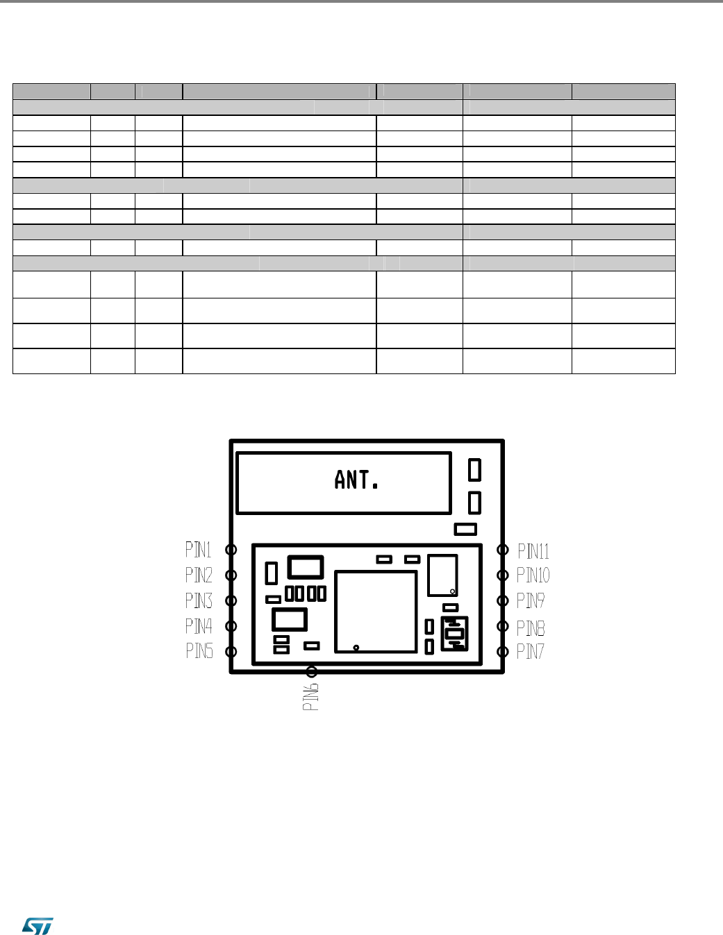
Pin connection diagram
SP
SGRF
Rev 1.0 P a g e | 7
Pin Assignment
Name Type Pin # Description
ALT Function
V
max.
Tolerant
Initial State
SPI Interface
SPI_CLK I 7 SPI CLOCK (Max. 8 MHz) V
in
SPI_MOSI I 9 SPI MOSI (MASTER out SLAVE in) V
in
SPI_MISO O 8 SPI MISO (MASTER in / SLAVE out) V
in
SPI_CS I 10 SPI “Chip Select” (SPI slave select) V
in
Power and Ground
V
in
5 V
in
(1.8V + 3.6V max.)
GND 6 GND
Module SHUTDOWN
SDN I 11 SHUTDOWN input (active high.) (1.8V + V
in
max).
GPIO – General Purpose Input/Output
GPIO [0] I/O 4 Programmable Input / Output
& Analog Temperature output
(1.8V + V
in
max.).
Digital Output
.
Low Power
GPIO [1] I/O 3 Programmable Input / Output (1.8V + V
in
max.).
Digital Output
.
Low Power
GPIO [2] I/O 2 Programmable Input / Output (1.8V + V
in
max.).
Digital Output
.
Low Power
GPIO [3] I/O 1 Programmable Input / Output (1.8V + V
in
max.).
Digital Output
.
Low Power
Pin1 = GPIO_3 (TBD) Pin11 = SDN
Pin2 = GPIO_2 (TBD) Pin10 = SPI_CS
Pin3 = GPIO_1 (TBD) Pin9 = SPI_MOSI
Pin4 = GPIO_0 (TBD) Pin8 = SPI_MISO
Pin5 = Vin Pin7 = SPI_CLK
Pin6 = GND

SPSGRF
P a g e | 8 Rev 1.0
Module Current Consumption
SPSGRF-868 module
Symbol
Parameter
T
est Conditions
Typ.
Unit
Idd Supply current
Operating mode
Tx , +11.6 dBm , 2-FSK , 868 MHz 22 mA
Operating mode
Tx , - 7 dBm , 2-FSK , 868 MHz 9 mA
Operating mode
Rx , 8685 MHz 10 mA
Command mode 0.6 mA
Shutdown High Level -Vdd
(with other I/O in High impedance) 0.1
µA
SPSGRF-915 module
Symbol
Parameter
T
est Conditions
Typ.
Unit
Idd Supply current
Operating mode
Tx , +11.6 dBm , 2-FSK , 915 MHz 22 mA
Operating mode
Tx , - 7 dBm , 2-FSK , 915 MHz 9 mA
Operating mode
Rx , 915 MHz 10 mA
Command mode 0.6 mA
Shutdown High Level -Vdd
(with other I/O in High impedance) 0.1
µA
Module RF compliance limits
The RF compliance limits are those tested for FCC and CE certification using the dedicated
DONGLE (PC92A.V01). These limits are enforced by the DONGLE firmware. Care must be taken
with custom application firmware to ensure these limits are not exceeded, voiding the FCC and CE
certification.
RF compliance limits table
Modulation
Standards
Parameter
Max.
Unit
2-FSK
GFSK
MSK
FCC Part 15.207
(1)
FCC Part 15.247
(1)
EN 300 220-2 V2.4.1
(2)
EN 301 489-01 V1.9.2
(2)
EN 301 489-03 V1.4.1
(2)
Data rate 500 kbps
Conducted
Output power +11.6 dBm
OOK
ASK
FCC Part 15.207
(1)
FCC Part 15.249
(1)
EN 300 220-2 V2.4.1
(2)
EN 301 489-01 V1.9.2
(2)
EN 301 489-03 V1.4.1
(2)
Data rate
250
kbps
Conducted
Output power 6 dBm
1. FCC standards are only applicable to the SPSGRF-915 module.
2. EN standards are only applicable to the SPSGRF-868 module.
SP
SGRF
Rev 1.0 P a g e | 9
Module RF typical performances
The RF performances of the SPSGRF-868 and SPSGRF-915 modules are depending from many
factors, related to the Customer hardware application board where the module is connected and
also to the Customer application firmware. To give some basic information to the Customer which
will be the module integrator, may be useful to furnish the RF measures taken in an anechoic
chamber using a dongle with inside connected the SPSGRF-868 or the SPSGRF-915 module.
SPSGRF-868 or 915 modules radiated typical performances
Symbol
Parameter
T
est Conditions
Typ.
Unit
Tx RF
power RF radiated
power
Operating mode
Tx , +11.6 dBm , 2-FSK , 868,0-868,6 MHz
5.3 dBm
Operating mode
Tx , +11.6 dBm , 2-FSK , 902-928 MHz 2.2 dBm
SPSGRF-868 or 915 modules conducted typical performances before the RF
antennas circuits (positive RF power signal values measured)
Parameter Test Condition
Conducted
Programmable
Value
Measured
conducted value
Typ. Unit
Tx RF
Conducted
Power
(before the
Antennas
circuits)
Operating mode
Tx , +11.6 dBm , 2-FSK , 868 MHz
Tx , +11.6 dBm , 2-FSK , 915 MHz 11.6 11.2 dBm
Operating mode
Tx , +11 dBm , 2-FSK , 868 MHz
Tx , +11 dBm , 2-FSK , 915 MHz 11.0 10.8 dBm
Operating mode
Tx , +10 dBm , 2-FSK , 868 MHz
Tx , +10 dBm , 2-FSK , 915 MHz 10.0 9.7 dBm
Operating mode
Tx , +9 dBm , 2-FSK , 868 MHz
Tx , +9 dBm , 2-FSK , 915 MHz 9.0 8.5 dBm
Operating mode
Tx , +8 dBm , 2-FSK , 868 MHz
Tx , +8 dBm , 2-FSK , 915 MHz 8.0 7.6 dBm
Operating mode
Tx , +7 dBm , 2-FSK , 868 MHz
Tx , +7 dBm , 2-FSK , 915 MHz 7.0 7.2 dBm
Operating mode
Tx , +6 dBm , 2-FSK , 868 MHz
Tx , +6 dBm , 2-FSK , 915 MHz 6.0 6.2 dBm
Operating mode
Tx , +5 dBm , 2-FSK , 868 MHz
Tx , +5 dBm , 2-FSK , 915 MHz 5.0 5.4 dBm
Operating mode
Tx , +4 dBm , 2-FSK , 868 MHz
Tx , +4 dBm , 2-FSK , 915 MHz 4.0 4.0 dBm
Operating mode
Tx , +3 dBm , 2-FSK , 868 MHz
Tx , +3 dBm , 2-FSK , 915 MHz 3.0 3.1 dBm
Operating mode
Tx , +2 dBm , 2-FSK , 868 MHz
Tx , +2 dBm , 2-FSK , 915 MHz 2.0 2.1 dBm
Operating mode
Tx , +1 dBm , 2-FSK , 868 MHz
Tx , +1 dBm , 2-FSK , 915 MHz
1.0
1.2 dBm
Operating mode
Tx , +0 dBm , 2-FSK , 868 MHz
Tx , +0 dBm , 2-FSK , 915 MHz 0.0 0.6 dBm
SPSGRF
P a g e | 10 Rev 1.0
SPSGRF-868 or 915 modules conducted typical performances before the RF
antennas circuits (negative RF power signal values measured)
Parameter Test Condition
Conducted
Programmable
Value
Measured
conducted value
Typ. Unit
Tx RF
Conducted
Power
(before the
Antennas
circuits)
Operating mode
Tx , -1 dBm , 2-FSK , 868 MHz
Tx , -1 dBm , 2-FSK , 915 MHz -1.0 -1.1 dBm
Operating mode
Tx , -2 dBm , 2-FSK , 868 MHz
Tx , -2 dBm , 2-FSK , 915 MHz -2.0 -2.3 dBm
Operating mode
Tx , -3 dBm , 2-FSK , 868 MHz
Tx , -3 dBm , 2-FSK , 915 MHz -3.0 -3.4 dBm
Operating mode
Tx , -4 dBm , 2-FSK , 868 MHz
Tx , -4 dBm , 2-FSK , 915 MHz -4.0 -4.9 dBm
Operating mode
Tx , -5 dBm , 2-FSK , 868 MHz
Tx , -5 dBm , 2-FSK , 915 MHz -5.0 -5.8 dBm
Operating mode
Tx , -6 dBm , 2-FSK , 868 MHz
Tx , -6 dBm , 2-FSK , 915 MHz
-6.0
-6.9 dBm
Operating mode
Tx , -7 dBm , 2-FSK , 868 MHz
Tx , -7 dBm , 2-FSK , 915 MHz
-7.0
-6.5 dBm
Operating mode
Tx , -8 dBm , 2-FSK , 868 MHz
Tx , -8 dBm , 2-FSK , 915 MHz
-8.0
-7.3 dBm
Operating mode
Tx , -9 dBm , 2-FSK , 868 MHz
Tx , -9 dBm , 2-FSK , 915 MHz
-9.0
-8.2 dBm
Operating mode
Tx , -10 dBm , 2-FSK , 868 MHz
Tx , -10 dBm , 2-FSK , 915 MHz
-10.0
-9.7 dBm
Operating mode
Tx , -15 dBm , 2-FSK , 868 MHz
Tx , -15 dBm , 2-FSK , 915 MHz
-15.0
-14,6 dBm
Operating mode
Tx , -20 dBm , 2-FSK , 868 MHz
Tx , -20 dBm , 2-FSK , 915 MHz
-20.0
-19.2 dBm
Operating mode
Tx , -25 dBm , 2-FSK , 868 MHz
Tx , -25 dBm , 2-FSK , 915 MHz
-25.0
-23.3 dBm
Operating mode
Tx , -30 dBm , 2-FSK , 868 MHz
Tx , -30 dBm , 2-FSK , 915 MHz
-30.0
-26.2 dBm
Operating mode
Tx , -35 dBm , 2-FSK , 868 MHz
Tx , -35 dBm , 2-FSK , 915 MHz
-35.0
-27.8 dBm
SP
SGRF
Rev 1.0 P a g e | 11
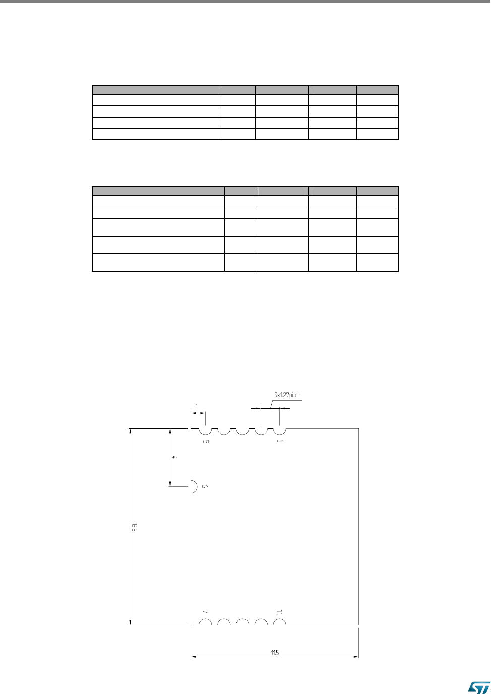
Mechanical dimensions
Recommend land pattern
PRELIMINARY
13.5 mm 2 mm
11.5 mm
Recommended land pattern top view
SPSGRF
P a g e | 12 Rev 1.0
6 Hardware design notes
SPSGRF-868 and SPSGRF-915 modules support SPI hardware interfaces.
Notes
All unused pins should be left floating; do not ground.
All GND pins must be well grounded.
The area around the module should be free of any ground planes, power planes, trace
routings, or metal for 6 mm from the module antenna position, in all directions.
Traces should not be routed underneath the module.
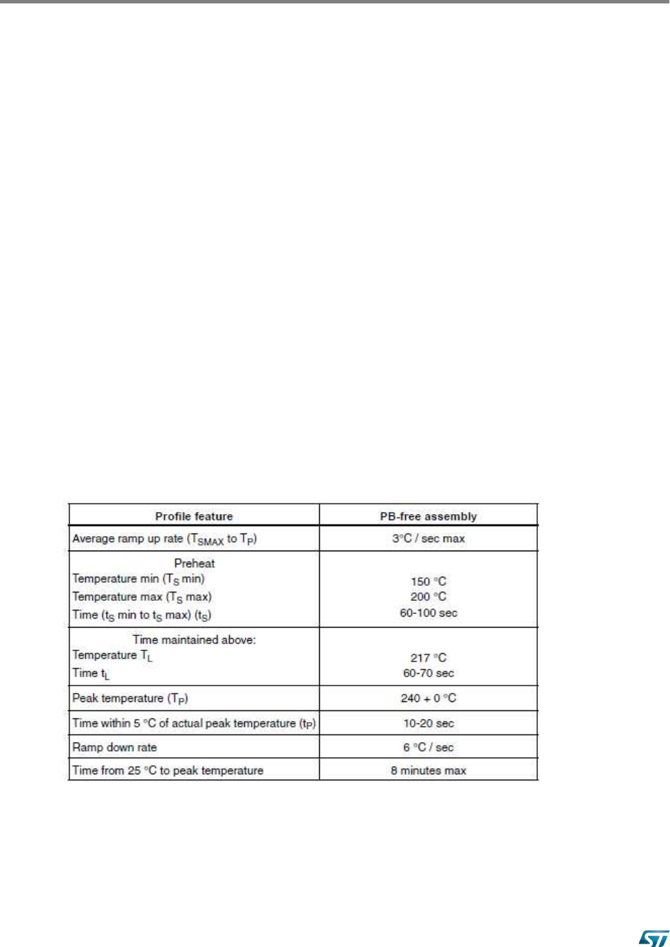
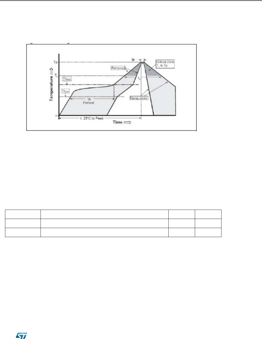
7 Reflow soldering
The SPSGRF is a surface mount SubGiga Transceiver module supplied on a 11 pin, 4-layer
PCB. The final assembly recommended reflow profiles are indicated here below.
Soldering phase has to be executed with care: In order to avoid undesired melting
phenomenon, particular attention has to be taken on the set up of the peak temperature.
Here following some suggestions for the temperature profile based on IPC/JEDEC
J-STD-020C, July 2004 recommendations.
Soldering
SP
SGRF
Rev 1.0 P a g e | 13
Soldering profiles
8 RoHS compliance
ST Bluetooth modules comply with the ECOPACK2 level of RoHS compliance grade.
9 Ordering Information
Order code Description Packing MOQ
SPSGRF-868 868 MHz Spirit1 transceiver module (Region 1,Europe) Jedec tray 2448 pcs
SPSGRF-915 915 MHz Spirit1 transceiver module (Region 2,The Americas) Jedec tray 2448 pcs

SPSGRF
P a g e | 14 Rev 1.0
10 Regulatory compliance
FCC certification
This module has been tested and found to comply with the FCC part 15 rules. These limits
are designed to provide reasonable protection against harmful interference in approved
installations. This equipment generates, uses, and can radiate radio frequency energy
and, if not installed and used in accordance with the instructions, may cause harmful
interference to radio communications.
However, there is no guarantee that interference may not occur in a particular installation.
This device complies with part 15 of the FCC rules. Operation is subject to the following
two conditions: (1) This device may not cause harmful interference, and (2) this device
must accept any interference received, including interference that may cause undesired
operation.
Modifications or changes to this equipment not expressly approved by STMicroelectronics
may render void the user's authority to operate this equipment.
Modular approval
FCC ID: S9NSPSGRF
In accordance with FCC part 15, the SPSGRF-915 is listed as a modular transmitter
device.
This module is evaluated for stand-alone use only. Finished products incorporating
multiple transmitters must comply with colocation and RF exposure requirements in
accordance with FCC multi-transmitter product procedures. Collocated transmitters
operating in portable RF Exposure conditions (e.g. <20cm from persons including but not
limited to body worn and hand held devices) may require separate approval.
Labeling instructions
When integrating the SPSGRF-915 into the final product, the OEM must ensure that the
FCC labeling requirements are satisfied. A statement must be included on the exterior of
the final product which indicates the product includes a certified module. The label should
state the following (or similar wording that conveys the same meaning):
Contains FCC ID: S9NSPSGRF
OR This product contains FCC ID: S9NSPSGRF
The OEM must include the following statements on the exterior of the final product unless
the product is too small (e.g. less than 4 x 4 inches):
This device complies with Part 15 of the FCC Rules. Operation is subject to the following
two conditions: (1) this device may not cause harmful interference, and (2) this device

SP
SGRF
Rev 1.0 P a g e | 15
must accept any interference received, including any interference that may cause
undesired operation.
Product manual instructions
This section applies to OEM final products containing the SPSGRF-915 module, subject to
FCC compliance. The final product manual must contain the following statement (or a
similar statement that conveys the same meaning):
WARNING: Changes or modifications not expressly approved by the party responsible
for compliance could void the user’s authority to operate the equipment. (Part. 15.21)
In the case where an OEM seeks Class B (residential) limits for the final product, the
following statement must be included in the final product manual:
NOTE: This equipment has been tested and found to comply with the limits for a Class B
digital device, pursuant to part 15 of the FCC Rules. These limits are designed to provide
reasonable protection against harmful interference in a residential installation. This
equipment generates, uses and can radiate radio frequency energy and, if not installed
and used in accordance with the instructions, may cause harmful interference to radio
communications. However, there is no guarantee that interference will not occur in a
particular installation. If this equipment does cause harmful interference to radio or
television reception, which can be determined by turning the equipment off and on, the
user is encouraged to try to correct the interference by one or more of the following
measures:
• Reorient or relocate the receiving antenna.
• Increase the separation between the equipment and receiver.
• Connect the equipment into an outlet on a circuit different from that to which the
receiver is connected.
• Consult the dealer or an experienced radio/TV technician for help.
In the case where an OEM seeks the lesser category of a Class A digital device for the final
product, the following statement must be included in the final product manual:
NOTE: This equipment has been tested and found to comply with the limits for a Class A
digital device, pursuant to part 15 of the FCC Rules. These limits are designed to provide
reasonable protection against harmful interference when the equipment is operated in a
commercial environment. This equipment generates, uses, and can radiate radio
frequency energy and, if not installed and used in accordance with the instruction manual,
may cause harmful interference to radio communications. Operation of this equipment in a
residential area is likely to cause harmful interference in which case the user will be
required to correct the interference at his expense.
SPSGRF
P a g e | 16 Rev 1.0
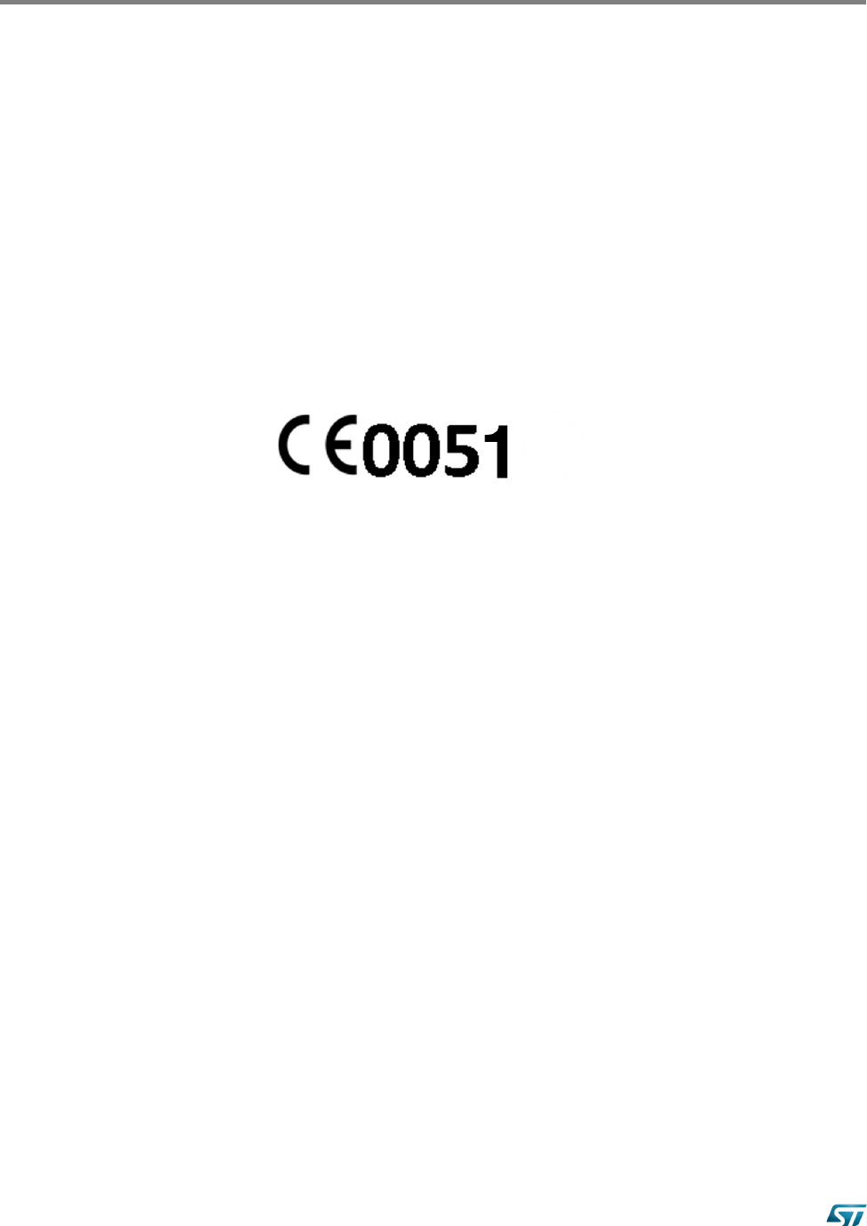
CE certification for SPSGRF-868 module
The SPSGRF-868 module has been certified according to the following standards:
EN 300 220-2 V2.4.1
EN 301 489-01 V1.9.2
EN 301 489-03 V1.4.1
EN60950-1:2006 + A11:2009 + A1:2010 + A12:2011
The module is CE certified:

SP
SGRF
Rev 1.0 P a g e | 17
Please Read Carefully:
Information in this document is provided solely in connection with ST products. STMicroelectronics NV and its subsidiaries (“ST”) reserve the
right to make changes, corrections, modifications or improvements, to this document, and the products and services described herein at any
time, without notice.
All ST products are sold pursuant to ST’s terms and conditions of sale.
Purchasers are solely responsible for the choice, selection and use of the ST products and services described herein, and ST assumes no
liability whatsoever relating to the choice, selection or use of the ST products and services described herein.
No license, express or implied, by estoppel or otherwise, to any intellectual property rights is granted under this document. If any part of this
document refers to any third party products or services it shall not be deemed a license grant by ST for the use of such third party products or
services, or any intellectual property contained therein or considered as a warranty covering the use in any manner whatsoever of such third
party products or services or any intellectual property contained therein.
UNLESS OTHERWISE SET FORTH IN ST’S TERMS AND CONDITIONS OF SALE ST DISCLAIMS ANY EXPRESS OR IMPLIED
WARRANTY WITH RESPECT TO THE USE AND/OR SALE OF ST PRODUCTS INCLUDING WITHOUT LIMITATION IMPLIED
WARRANTIES OF MERCHANTABILITY, FITNESS FOR A PARTICULAR PURPOSE (AND THEIR EQUIVALENTS UNDER THE LAWS
OF ANY JURISDICTION), OR INFRINGEMENT OF ANY PATENT, COPYRIGHT OR OTHER INTELLECTUAL PROPERTY RIGHT.
ST PRODUCTS ARE NOT DESIGNED OR AUTHORIZED FOR USE IN: (A) SAFETY CRITICAL APPLICATIONS SUCH AS LIFE
SUPPORTING, ACTIVE IMPLANTED DEVICES OR SYSTEMS WITH PRODUCT FUNCTIONAL SAFETY REQUIREMENTS; (B)
AERONAUTIC APPLICATIONS; (C) AUTOMOTIVE APPLICATIONS OR ENVIRONMENTS, AND/OR (D) AEROSPACE APPLICATIONS
OR ENVIRONMENTS. WHERE ST PRODUCTS ARE NOT DESIGNED FOR SUCH USE, THE PURCHASER SHALL USE PRODUCTS AT
PURCHASER’S SOLE RISK, EVEN IF ST HAS BEEN INFORMED IN WRITING OF SUCH USAGE, UNLESS A PRODUCT IS EXPRESSLY
DESIGNATED BY ST AS BEING INTENDED FOR “AUTOMOTIVE, AUTOMOTIVE SAFETY OR MEDICAL” INDUSTRY DOMAINS
ACCORDING TO ST PRODUCT DESIGN SPECIFICATIONS. PRODUCTS FORMALLY ESCC, QML OR JAN QUALIFIED ARE DEEMED
SUITABLE FOR USE IN AEROSPACE BY THE CORRESPONDING GOVERNMENTAL AGENCY.
Resale of ST products with provisions different from the statements and/or technical features set forth in this document shall immediately void
any warranty granted by ST for the ST product or service described herein and shall not create or extend in any manner whatsoever, any
liability of ST.
ST and the ST logo are trademarks or registered trademarks of ST in various countries.
Information in this document supersedes and replaces all information previously supplied.
The ST logo is a registered trademark of STMicroelectronics. All other names are the property of their respective owners.
© 2013 STMicroelectronics - All rights reserved
STMicroelectronics group of companies
Australia - Belgium - Brazil - Canada - China - Czech Republic - Finland - France - Germany - Hong Kong - India - Israel - Italy - Japan -
Malaysia - Malta - Morocco - Philippines - Singapore - Spain - Sweden - Switzerland - United Kingdom - United States of America
www.st.com