ST Microelectronics S R L SPWFS04 SPWF04SA / C Wi-Fi Module User Manual Serial to Wi Fi b g n intelligent modules
ST Microelectronics S.R.L. SPWF04SA / C Wi-Fi Module Serial to Wi Fi b g n intelligent modules
UserManual.wiki
>
ST Microelectronics S R L
>
SPWFS04 User Manual
Users manual
Navigation menu
Upload a User Manual
Namespaces
Wiki Guide
HTML
PDF
Info
Views
User Manual
Discussion / Help
Navigation
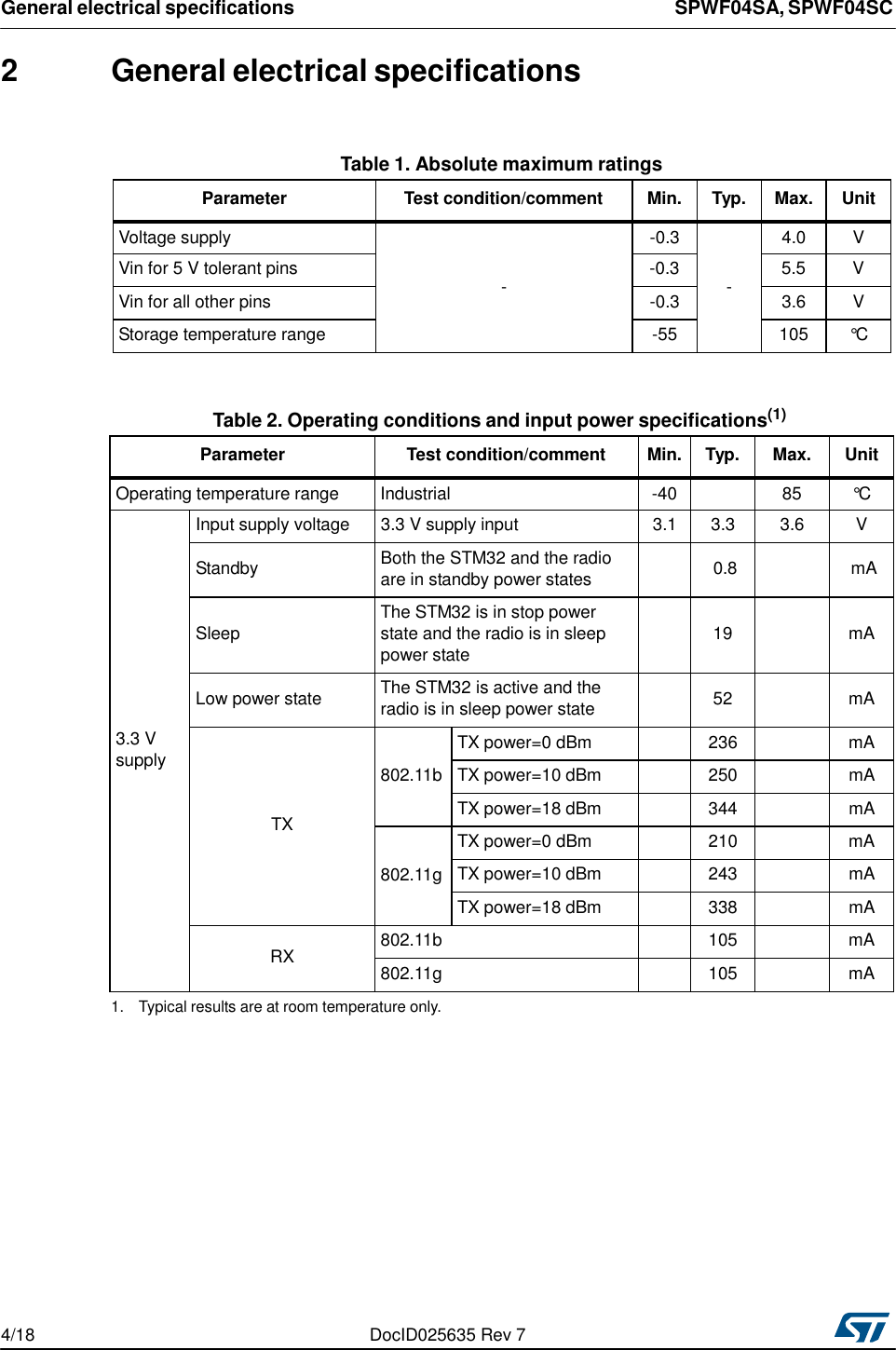
![SPWF04SA, SPWF04SC Pinout description 5 Pinout description Table 5. Pinout description Signal name Type Pin number Main function Alternate functions(1) Notes GPIO - general purpose input/output GPIO[0] I/O 16 General purpose input/output Restore to factory settings(2) Input pull down and 5V tolerant GPIO[1] I/O 17 General purpose input/output/ADC Input pull down and 5V tolerant GPIO[2] I/O 19 General purpose input/output/PWM Floating and 5V tolerant GPIO[3] I/O 1 General purpose input/output Input pull down and 5V tolerant GPIO[6] I/O 22 General purpose input/output Wake Up/Sleep Inhibit(3) Input pull down and 5V tolerant GPIO[4] I/O 18 General purpose input/output GPIO[5] I/O 20 General purpose input/output GPIO[7] I/O 13 General purpose input/output STA/Mini AP Switch/WPS Pushbutton (4) GPIO[8] I/O 4 General purpose input/output GPIO[9] I/O 7 General purpose input/output/SPI nHostInterrupt GPIO[11] I/O 11 GPIO[12] I/O 12 General purpose input/output GPIO[15] I/O 21 General purpose input/output/DAC Monitoring purpose with no alternate function GPIO[10] I/O 5 Drives LED, Blinks while running GPIO[13] I/O 15 Drives LED, Wi-Fi link up DocID025635 Rev 7 7/18](https://usermanual.wiki/ST-Microelectronics-S-R-L/SPWFS04/User-Guide-3029968-Page-7.png)
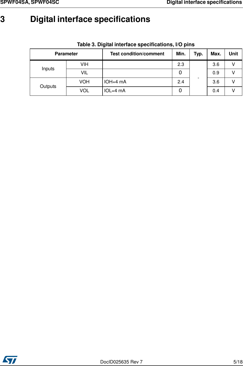
![Pinout description SPWF04SA, SPWF04SC Table 5. Pinout description (continued) Signal name Type Pin number Main function Alternate functions(1) Notes GPIO[14] I/O 14 LED drive, Power up UART pins RXD / MOSI I 8 5V tolerant TXD / MISO 6 5V Tolerant CTS / nCS I 9 Active low, 5V tolerant RTS / CLK O 10 5V tolerant Reset RESETn I 3 Reset input Active low for 5 ms with pull up to 2.5VDC. Not 5V tolerant Supply pins and paddle 3.3 V 24 Voltage supply Decouple with 10uF capacitor Ground 23 Ground LSE 34 HSE 35 SWD I/O 26 SWD CLK 29 GPIO16 27 Not available GPIO17 28 Not available GPIO18 30 Not available SDIO CLK / SPI CLK 31 SDIO D0 / SPI MISO 32 SDIO CMD / SPI MOSI 33 Ground Paddle 25 Ground Add plenty of ground vias for thermal dissipation and ground return Boot loader BOOT0 I 2 Boot loader (5) 1. The activation of ALT function depends upon the firmware version or upon the variable configuration. 2. To perform the factory reset of the variables, pin GPIO0 must be high during powerup. 3. GPIO function running when low power mode variable is enabled. 4. Introduced with the release 3.0 of AT Full stack. To enable the STAToMiniAP switch the GPIO[7] needs to be put low together with the HW reset 8/18 DocID025635 Rev 7](https://usermanual.wiki/ST-Microelectronics-S-R-L/SPWFS04/User-Guide-3029968-Page-8.png)