STMicroelectronicsS DEMOCR95HF RFID Reader User Manual UM1589
STMicroelectronics RFID Reader UM1589
UserManual.wiki
>
STMicroelectronicsS
>
DEMOCR95HF User Manual
User Manual
Navigation menu
Upload a User Manual
Namespaces
Wiki Guide
HTML
PDF
Info
Views
User Manual
Discussion / Help
Navigation
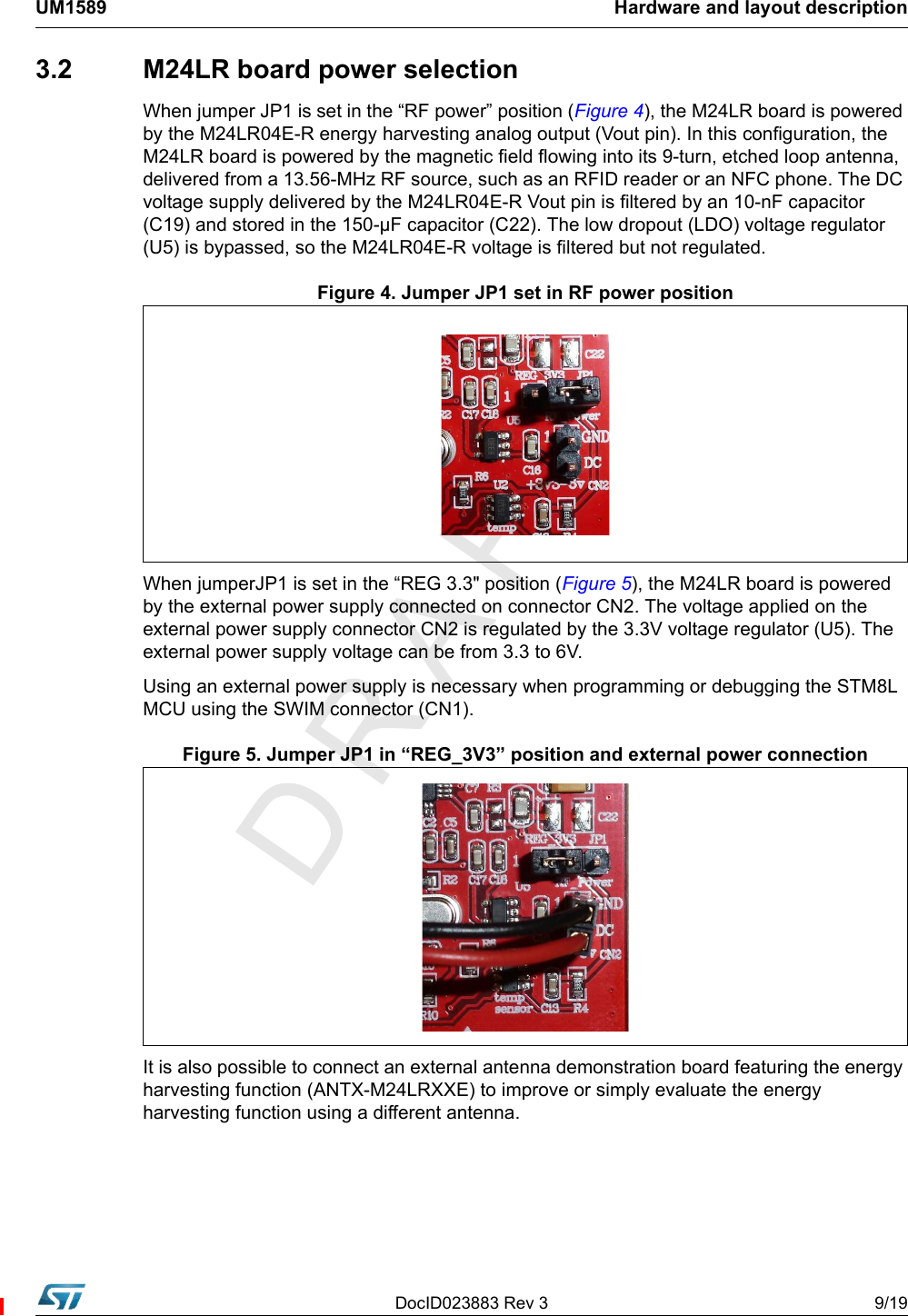
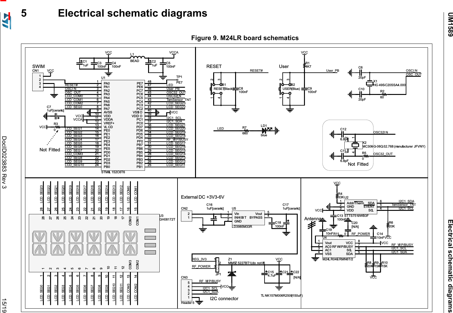
![DocID023883 Rev 3 5/19UM1589 Quick start1 Quick startThe M24LR-DISCOVERY kit is a low-cost and ready-to-use development kit used to evaluate the functions and performance of the M24LR Dual Interface EEPROM family and its energy harvesting capability.For more information on the M24LR-DISCOVERY kit and associated demonstration software, please visit www.st.com/m24lr04e-discovery.1.1 Getting started with the M24LR04E Dual Interface EEPROM1. On the M24LR board, ensure that a jumper is placed on connector JP1 in the RF power position (jumper on the right side as shown in Figure 4). 2. Download and install the M24LR/CR95 application software setup file [STSW-M24LR011] available at www.st.com/m24lr04e-discovery.3. Connect the RF transceiver demo board to a PC with a USB cable.4. Launch setup.exe, and select CR95HF Demo Kit. Then, open the Demo NDEF messages menu and select Show Demo NDEF & Energy Harvesting.5. Place the M24LR board antenna close to the RF transceiver demo board antenna.6. The M24LR board starts in Message Display mode (The “M24LR04E-DISCOVERY” message scrolls across the screen from right to left).You can read the current NDEF message stored in the M24LR04E-R by clicking the Read NDEF message button of the PC software.You can also write an new NDEF message: it will be automatically displayed on the M24LR board LCD screen after programming.7. To change the user mode, press push button B2 (blue button on the left side of the board). Table 2 lists the user modes available. To study or modify the M24LR board application project related to this demo, please visit dedicated webpages on www.st.com/m24lr04e-discovery.Table 2. Available user modesMode Description1 Displays the NDEF text message stored in the M24LR04E Dual Interface EEPROM.2 Displays the voltage powering the M24LR board.3 Displays the ambient temperature, measured using the temperature sensor.](https://usermanual.wiki/STMicroelectronicsS/DEMOCR95HF/User-Guide-2539324-Page-5.png)
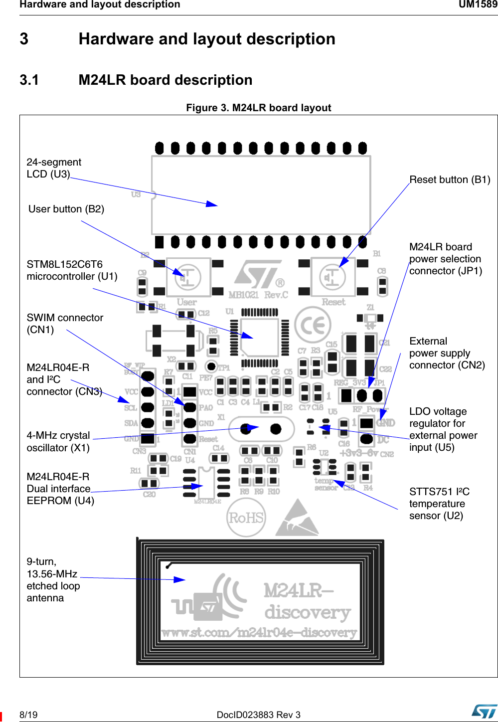
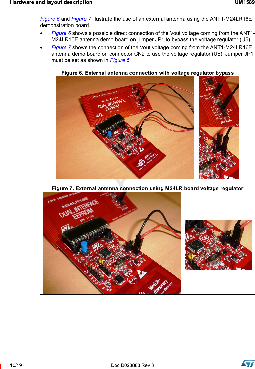
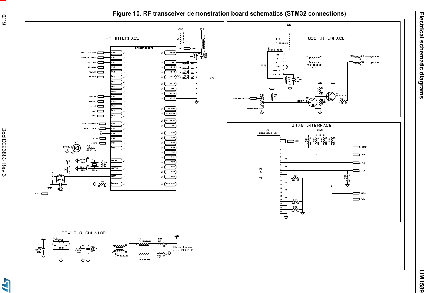
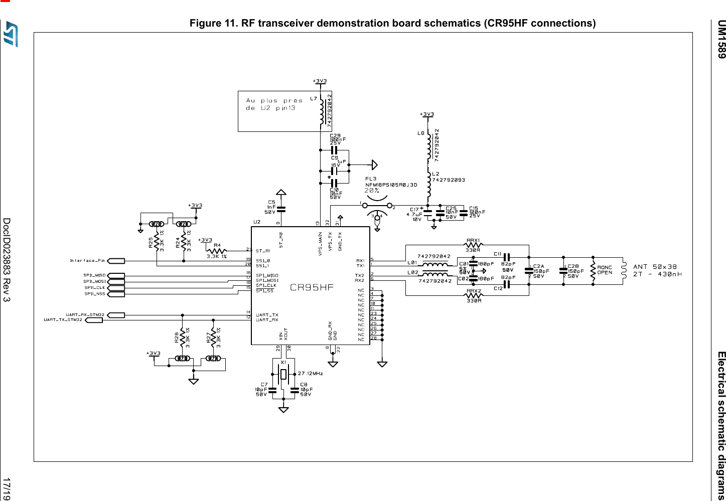
![DocID023883 Rev 3 11/19UM1589 Hardware and layout description3.3 RF transceiver board descriptionFigure 8. RF transceiver board layout (top and bottom)3.4 RF transceiver demonstration board powering and startupThe RF transceiver demonstration board is powered by the USB bus.When powered up, the CR95HF starts in an autonomous mode called “tag hunting”: the red LED 1 lights up every time a tag is recognized. During Tag Hunting mode, the RF transceiver demonstration board switches ON and OFF the magnetic field at each RF protocol change. A constant magnetic field is naturally more appropriate to evaluate and develop battery-less applications based on the Energy Harvesting capability of the M24LRXXE-R EEPROM Family.Tag Hunting mode persists until the M24LR/CR95 application software setup file [STSW-M24LR011] is launched and the CR95HF is initialized by the software. At this moment, both Tag Hunting mode and the RF field stop. To activate a constant magnetic field emission, it possible either to open the Demo NDEF messages menu and select Show Demo NDEF & Energy Harvesting or send a single ISO/IEC15693 RF command (Inventory, Read.). 2-turn,13.56-MHzloop antennaReset button27.12-MHzcrystal oscillator20-pin JTAGconnector (J3)STM32F103CBT6User LED 1LDO regulatorUSB connector (J1)CR95HF RF IC](https://usermanual.wiki/STMicroelectronicsS/DEMOCR95HF/User-Guide-2539324-Page-11.png)
![Revision history UM158918/19 DocID023883 Rev 36 Revision history Table 4. Document revision historyDate Revision Changes06-Nov-2012 1Initial release.11-Mar-2013 2Replaced “M24LR/CR95HF demonstration software " by "M24LR/CR95 application software setup file [STSW-M24LR011]" in Section 1.1 and Section 3.4.Replaced “M24LRxx_Application_Software.exe” by “setup.exe” in Section 1.1.dd-Feb-2015 3Updated Figure 1: M24LR evaluation board andFigure 2: RF transceiver demonstration board. Added Section 4: Federal Communications Commission (FCC) and Industry Canada (IC) Compliance Statements.](https://usermanual.wiki/STMicroelectronicsS/DEMOCR95HF/User-Guide-2539324-Page-18.png)