STMicroelectronicsS DEMOCR95HF RFID Reader User Manual UM1589
STMicroelectronics RFID Reader UM1589
User Manual
13 February 2015 DocID023883 Rev 3 1/19
UM1589
User manual
M24LR-DISCOVERY kit user guide
Introduction
The M24LR-DISCOVERY kit helps you evaluate the M24LRXX-E Dual Interface EEPROM that features
an energy harvesting analog output, as well as a user-configurable digital output.
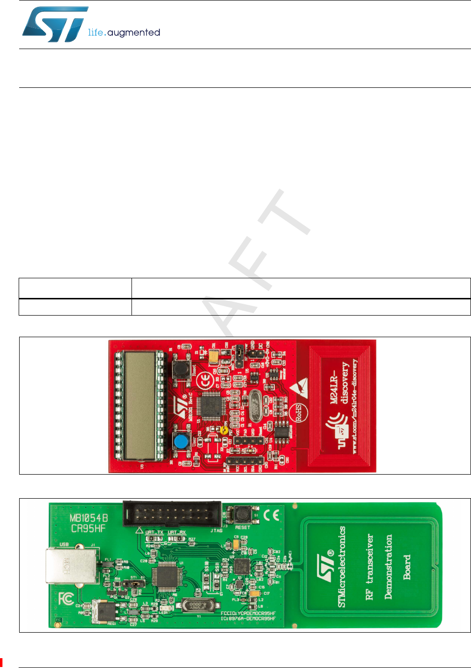
The M24LR-DISCOVERY kit is delivered with a battery-less M24LR board that can be powered by RFID
readers or NFC phones supporting the ISO/IEC15693 protocol. It is based on an M24LR04E-R I²C -
ISO/IEC15693 Dual Interface EEPROM, an 8-bit STM8L152C6T6 ultralow power microcontroller, and
includes an STTS751 temperature sensor, a 24-segment LCD, and 2 push buttons.
The M24LR-DISCOVERY kit also comes with an USB RF transceiver demonstration board that includes
the CR95HF 13.56-MHz multi-protocol contactless transceiver. It is based on a 32-bit, STM32F103CBT6
performance line microcontroller and is connected to a computer host via its USB connector.
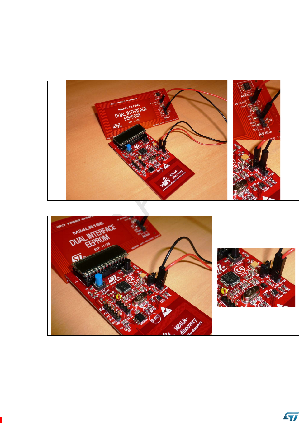
Figure 1. M24LR evaluation board
Figure 2. RF transceiver demonstration board
Table 1. Applicable tools
Type Applicable tool
Evaluation tools M24LR-DISCOVERY
www.st.com

Contents UM1589
2/19 DocID023883 Rev 3
Contents
1 Quick start . . . . . . . . . . . . . . . . . . . . . . . . . . . . . . . . . . . . . . . . . . . . . . . . . 5
1.1 Getting started with the M24LR04E Dual Interface EEPROM . . . . . . . . . . 5
1.2 Using the M24LR board with Android NFC phones . . . . . . . . . . . . . . . . . . 6
1.3 System requirements . . . . . . . . . . . . . . . . . . . . . . . . . . . . . . . . . . . . . . . . . 6
1.4 Development toolchain . . . . . . . . . . . . . . . . . . . . . . . . . . . . . . . . . . . . . . . . 6
2 Features . . . . . . . . . . . . . . . . . . . . . . . . . . . . . . . . . . . . . . . . . . . . . . . . . . . 7
3 Hardware and layout description . . . . . . . . . . . . . . . . . . . . . . . . . . . . . . . 8
3.1 M24LR board description . . . . . . . . . . . . . . . . . . . . . . . . . . . . . . . . . . . . . . 8
3.2 M24LR board power selection . . . . . . . . . . . . . . . . . . . . . . . . . . . . . . . . . . 9
3.3 RF transceiver board description . . . . . . . . . . . . . . . . . . . . . . . . . . . . . . . .11
3.4 RF transceiver demonstration board powering and startup . . . . . . . . . . . .11
3.5 Program/debug the M24LR board . . . . . . . . . . . . . . . . . . . . . . . . . . . . . . 12
3.6 Program/debug the RF transceiver demo board . . . . . . . . . . . . . . . . . . . 12
4 Federal Communications Commission (FCC) and Industry Canada (IC)
Compliance Statements 13
4.1 FCC Compliance Statement . . . . . . . . . . . . . . . . . . . . . . . . . . . . . . . . . . . 13
4.1.1 Part 15.19 . . . . . . . . . . . . . . . . . . . . . . . . . . . . . . . . . . . . . . . . . . . . . . . 13
4.1.2 Part 15.105 . . . . . . . . . . . . . . . . . . . . . . . . . . . . . . . . . . . . . . . . . . . . . . 13
4.1.3 Part 15.21 . . . . . . . . . . . . . . . . . . . . . . . . . . . . . . . . . . . . . . . . . . . . . . . 13
4.2 IC Compliance Statement . . . . . . . . . . . . . . . . . . . . . . . . . . . . . . . . . . . . . 13
4.3 IC Déclaration de conformité . . . . . . . . . . . . . . . . . . . . . . . . . . . . . . . . . . 13
5 Electrical schematic diagrams . . . . . . . . . . . . . . . . . . . . . . . . . . . . . . . . 15
6 Revision history . . . . . . . . . . . . . . . . . . . . . . . . . . . . . . . . . . . . . . . . . . . 18

DocID023883 Rev 3 3/19
UM1589 List of tables
3
List of tables
Table 1. Applicable tools. . . . . . . . . . . . . . . . . . . . . . . . . . . . . . . . . . . . . . . . . . . . . . . . . . . . . . . . . . . 1
Table 2. Available user modes . . . . . . . . . . . . . . . . . . . . . . . . . . . . . . . . . . . . . . . . . . . . . . . . . . . . . . 5
Table 3. M24LR board programming and debug connector . . . . . . . . . . . . . . . . . . . . . . . . . . . . . . . 12
Table 4. Document revision history . . . . . . . . . . . . . . . . . . . . . . . . . . . . . . . . . . . . . . . . . . . . . . . . . 18

List of figures UM1589
4/19 DocID023883 Rev 3
List of figures
Figure 1. M24LR evaluation board. . . . . . . . . . . . . . . . . . . . . . . . . . . . . . . . . . . . . . . . . . . . . . . . . . . . 1
Figure 2. RF transceiver demonstration board . . . . . . . . . . . . . . . . . . . . . . . . . . . . . . . . . . . . . . . . . . 1
Figure 3. M24LR board layout . . . . . . . . . . . . . . . . . . . . . . . . . . . . . . . . . . . . . . . . . . . . . . . . . . . . . . . 8
Figure 4. Jumper JP1 set in RF power position . . . . . . . . . . . . . . . . . . . . . . . . . . . . . . . . . . . . . . . . . . 9
Figure 5. Jumper JP1 in “REG_3V3” position and external power connection . . . . . . . . . . . . . . . . . . 9
Figure 6. External antenna connection with voltage regulator bypass. . . . . . . . . . . . . . . . . . . . . . . . 10
Figure 7. External antenna connection using M24LR board voltage regulator . . . . . . . . . . . . . . . . . 10
Figure 8. RF transceiver board layout (top and bottom) . . . . . . . . . . . . . . . . . . . . . . . . . . . . . . . . . . 11
Figure 9. M24LR board schematics . . . . . . . . . . . . . . . . . . . . . . . . . . . . . . . . . . . . . . . . . . . . . . . . . . 15
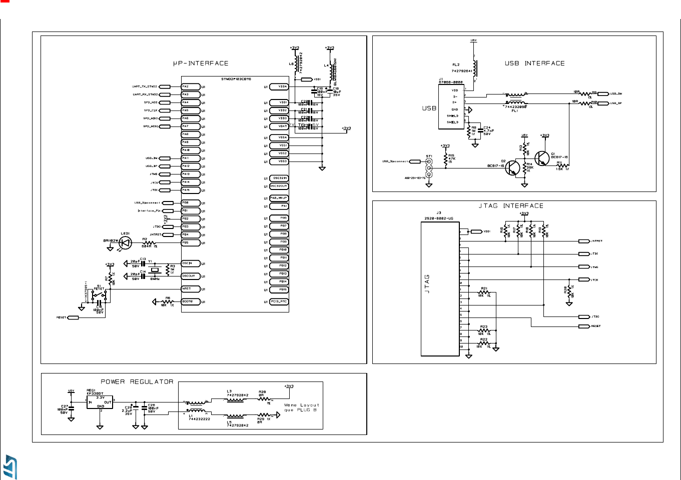
Figure 10. RF transceiver demonstration board schematics (STM32 connections) . . . . . . . . . . . . . . 16
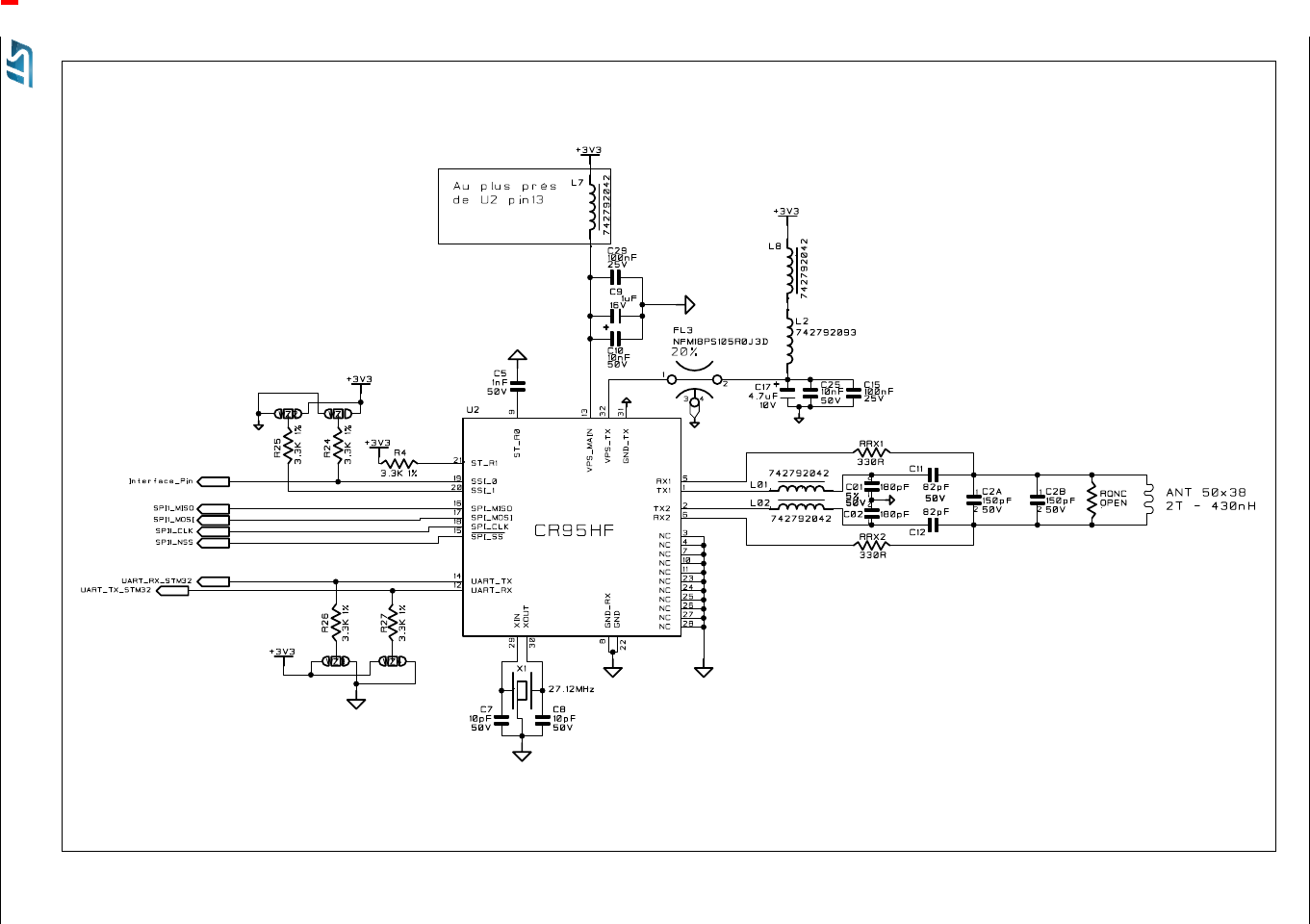
Figure 11. RF transceiver demonstration board schematics (CR95HF connections) . . . . . . . . . . . . . 17
DocID023883 Rev 3 5/19
UM1589 Quick start
1 Quick start
The M24LR-DISCOVERY kit is a low-cost and ready-to-use development kit used to
evaluate the functions and performance of the M24LR Dual Interface EEPROM family and
its energy harvesting capability.
For more information on the M24LR-DISCOVERY kit and associated demonstration
software, please visit www.st.com/m24lr04e-discovery.
1.1 Getting started with the M24LR04E Dual Interface EEPROM
1. On the M24LR board, ensure that a jumper is placed on connector JP1 in the RF power
position (jumper on the right side as shown in Figure 4).
2. Download and install the M24LR/CR95 application software setup file [STSW-
M24LR011] available at www.st.com/m24lr04e-discovery.
3. Connect the RF transceiver demo board to a PC with a USB cable.
4. Launch setup.exe, and select CR95HF Demo Kit. Then, open the Demo NDEF
messages menu and select Show Demo NDEF & Energy Harvesting.
5. Place the M24LR board antenna close to the RF transceiver demo board antenna.
6. The M24LR board starts in Message Display mode (The “M24LR04E-DISCOVERY”
message scrolls across the screen from right to left).
You can read the current NDEF message stored in the M24LR04E-R by clicking the
Read NDEF message button of the PC software.
You can also write an new NDEF message: it will be automatically displayed on the
M24LR board LCD screen after programming.
7. To change the user mode, press push button B2 (blue button on the left side of the
board). Table 2 lists the user modes available.
To study or modify the M24LR board application project related to this demo, please visit
dedicated webpages on www.st.com/m24lr04e-discovery.
Table 2. Available user modes
Mode Description
1 Displays the NDEF text message stored in the M24LR04E Dual Interface EEPROM.
2 Displays the voltage powering the M24LR board.
3 Displays the ambient temperature, measured using the temperature sensor.

Quick start UM1589
6/19 DocID023883 Rev 3
1.2 Using the M24LR board with Android NFC phones
1. Enable NFC communication on your phone (Settings >Wireless and Networks>NFC).
2. Download the NfcV-Reader Application from Google Play Store.
3. Launch the NfcV-Reader application.
4. Place the phone's NFC antenna close to the M24LR board antenna.
The phone powers the M24LR board.
The text message can be changed in the M24LR04E using the NFC phone (select NDEF
function in the NfcV-Reader application and open the Write NDEF message menu).
Please note that performance may vary depending on the NFC phone and its RF
management system.
1.3 System requirements
•Windows® PC (XP or Vista)
•Two USB cables
1.4 Development toolchain
•Cosmic CXSTM8 compiler
•STMicroelectronics ST Visual Develop (STVD) integrated development environment
•STMicroelectronics STLINK/V2 in-circuit debugger and programmer

DocID023883 Rev 3 7/19
UM1589 Features
2 Features
The M24LR-DISCOVERY kit includes M24LR board and the RF transceiver board
which offer the following features.
M24LR board
•M24LR04E-R, a 4-Kbit EEPROM with an I²C-ISO/IEC 15693 dual interface and an
energy harvesting analog output (Vout pin) and a user-configurable digital output (RF
Write-in-progress or Busy pin) in an SO8N package
•9-turn, 13.56-MHz etched antenna (20mm x 40mm) for RF powering and
communication
•STM8L152C6T6, 8-bit ultralow power microcontroller with up to 32 Kbytes of Flash
memory, 2 Kbytes of RAM, and 1 Kbyte of Data EEPROM in a 48-pin LQFP package
•STTS751 I²C low power temperature sensor
•28-pin LCD on DIP24 socket (24 segments, 4 commons)
•Two push buttons (User and Reset)
•HC-49S-C20SSA, a 4-MHz crystal oscillator (not used in demonstration firmware)
•4-pin connector (CN1) for STM8L programming and debug (SWIM)
•2-pin connector (CN2) for external power supply source (3 to 6V)
•5-pin connector (CN3) for M24LR04E-R and I²C bus probing
•3-pin switch (JP1) to select M24LR board power source (M24LR04E Vout pin or
external)
RF transceiver board
•CR95HF, a 13.56-MHz multi-protocol contactless transceiver IC with SPI and UART
serial access communication
•2-turn, 13.56-MHz etched loop antenna (47mm x 34 mm) with associated tuning circuit
and lowpass filter
•STM32F103CBT6, a 32-bit microcontroller with 128 Kbytes of Flash memory and USB
interface in a 48-pin LQFP package
•KF33BDT, a 3.3V low dropout (LDO) voltage regulator
•USB connector
•NX2520SA, a 27.12-MHz EXS00A-CS01206 crystal oscillator for CR95HF transceiver
•HC-49XA-C20QQA-8.000MHz for STM32
•20-pin JTAG connector for STM32 programming and debugging
•1 push button (Reset)
Hardware and layout description UM1589
8/19 DocID023883 Rev 3
3 Hardware and layout description
3.1 M24LR board description
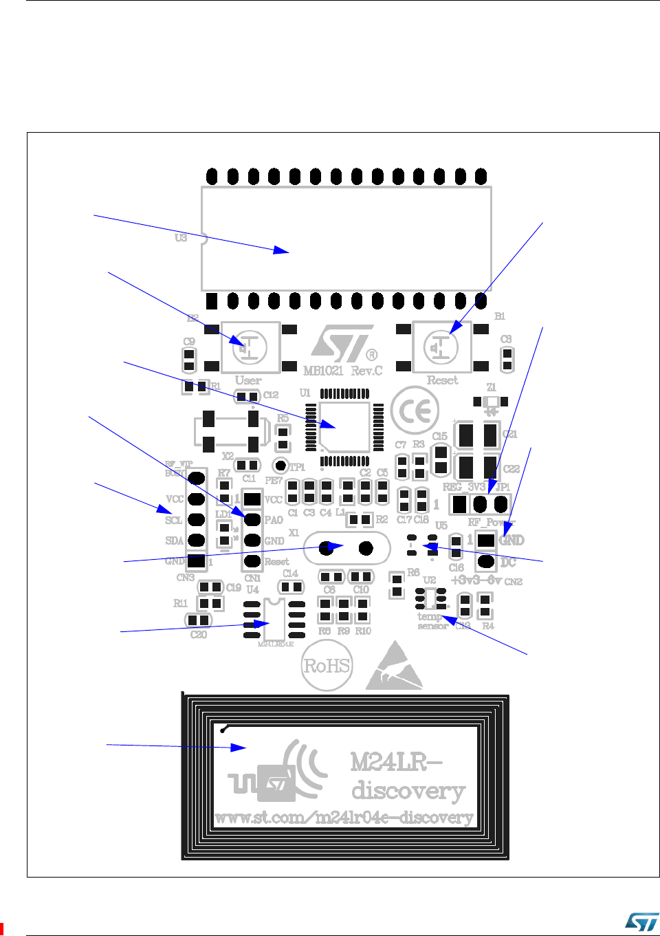
Figure 3. M24LR board layout
STM8L152C6T6
SWIM connector
M24LR04E-R
4-MHz crystal
M24LR04E-R
9-turn,
Reset button (B1)
M24LR board
External
LDO voltage
STTS751 I²C
temperature
sensor (U2)
regulator for
external power
input (U5)
power supply
connector (CN2)
power selection
connector (JP1)
13.56-MHz
etched loop
antenna
Dual interface
EEPROM (U4)
oscillator (X1)
and I²C
connector (CN3)
(CN1)
microcontroller (U1)
24-segment
LCD (U3)
User button (B2)
DocID023883 Rev 3 9/19
UM1589 Hardware and layout description
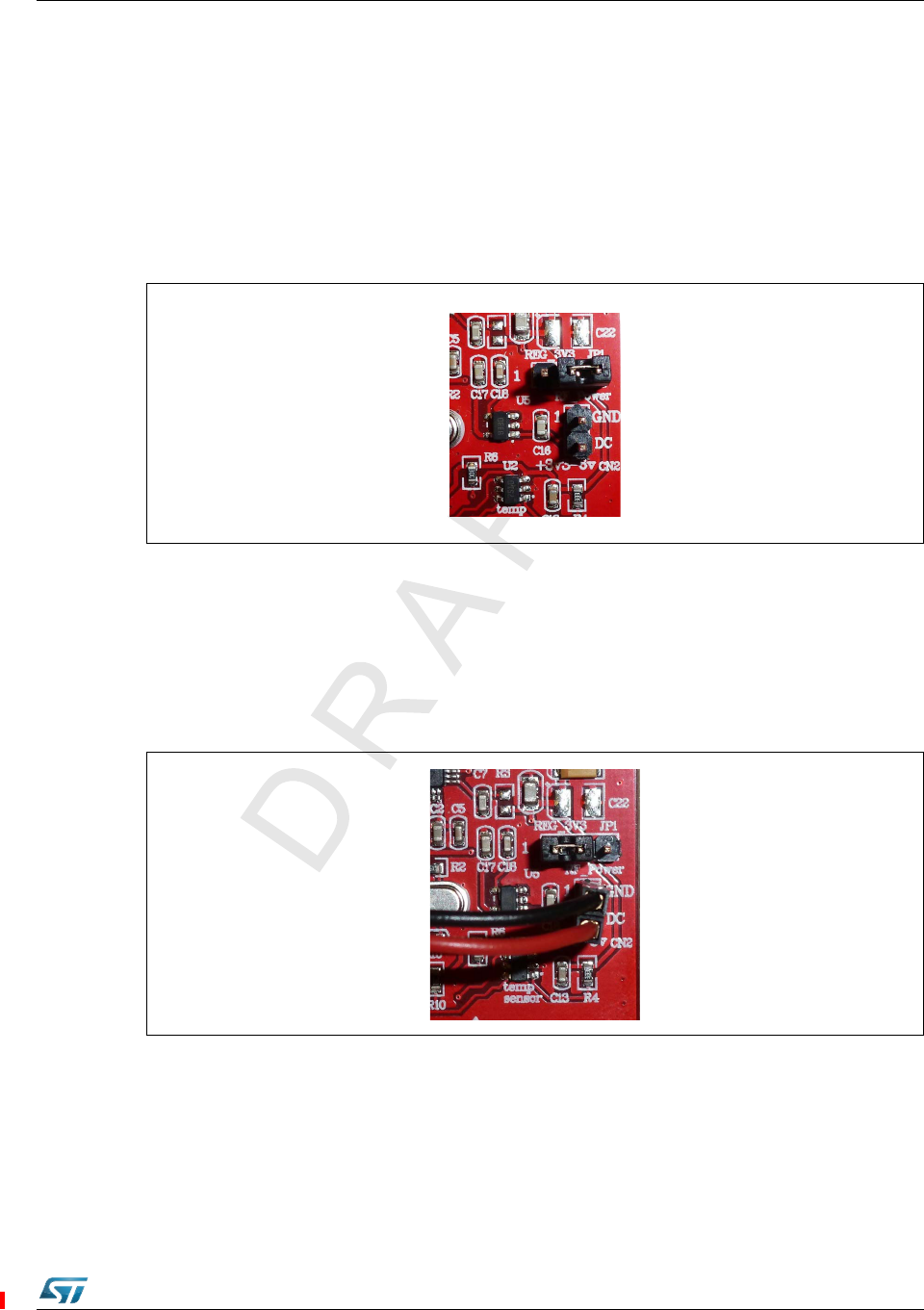
3.2 M24LR board power selection
When jumper JP1 is set in the “RF power” position (Figure 4), the M24LR board is powered
by the M24LR04E-R energy harvesting analog output (Vout pin). In this configuration, the
M24LR board is powered by the magnetic field flowing into its 9-turn, etched loop antenna,
delivered from a 13.56-MHz RF source, such as an RFID reader or an NFC phone. The DC
voltage supply delivered by the M24LR04E-R Vout pin is filtered by an 10-nF capacitor
(C19) and stored in the 150-µF capacitor (C22). The low dropout (LDO) voltage regulator
(U5) is bypassed, so the M24LR04E-R voltage is filtered but not regulated.
Figure 4. Jumper JP1 set in RF power position
When jumperJP1 is set in the “REG 3.3" position (Figure 5), the M24LR board is powered
by the external power supply connected on connector CN2. The voltage applied on the
external power supply connector CN2 is regulated by the 3.3V voltage regulator (U5). The
external power supply voltage can be from 3.3 to 6V.
Using an external power supply is necessary when programming or debugging the STM8L
MCU using the SWIM connector (CN1).
Figure 5. Jumper JP1 in “REG_3V3” position and external power connection
It is also possible to connect an external antenna demonstration board featuring the energy
harvesting function (ANTX-M24LRXXE) to improve or simply evaluate the energy
harvesting function using a different antenna.
Hardware and layout description UM1589
10/19 DocID023883 Rev 3
Figure 6 and Figure 7 illustrate the use of an external antenna using the ANT1-M24LR16E
demonstration board.
•Figure 6 shows a possible direct connection of the Vout voltage coming from the ANT1-
M24LR16E antenna demo board on jumper JP1 to bypass the voltage regulator (U5).
•Figure 7 shows the connection of the Vout voltage coming from the ANT1-M24LR16E
antenna demo board on connector CN2 to use the voltage regulator (U5). Jumper JP1
must be set as shown in Figure 5.
Figure 6. External antenna connection with voltage regulator bypass
Figure 7. External antenna connection using M24LR board voltage regulator
DocID023883 Rev 3 11/19
UM1589 Hardware and layout description
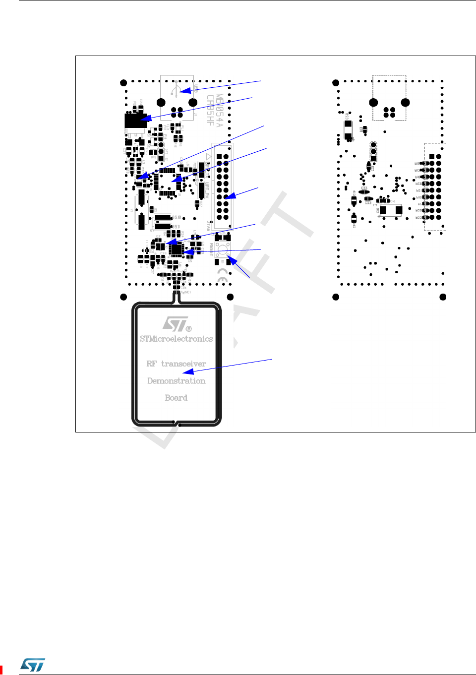
3.3 RF transceiver board description
Figure 8. RF transceiver board layout (top and bottom)
3.4 RF transceiver demonstration board powering and startup
The RF transceiver demonstration board is powered by the USB bus.
When powered up, the CR95HF starts in an autonomous mode called “tag hunting”: the red
LED 1 lights up every time a tag is recognized. During Tag Hunting mode, the RF
transceiver demonstration board switches ON and OFF the magnetic field at each RF
protocol change. A constant magnetic field is naturally more appropriate to evaluate and
develop battery-less applications based on the Energy Harvesting capability of the
M24LRXXE-R EEPROM Family.
Tag Hunting mode persists until the M24LR/CR95 application software setup file [STSW-
M24LR011] is launched and the CR95HF is initialized by the software. At this moment, both
Tag Hunting mode and the RF field stop. To activate a constant magnetic field emission, it
possible either to open the Demo NDEF messages menu and select Show Demo NDEF &
Energy Harvesting or send a single ISO/IEC15693 RF command (Inventory, Read.).
2-turn,13.56-MHz
loop antenna
Reset button
27.12-MHz
crystal oscillator
20-pin JTAG
connector (J3)
STM32F103CBT6
User LED 1
LDO regulator
USB
connector (J1)
CR95HF RF IC
Hardware and layout description UM1589
12/19 DocID023883 Rev 3
3.5 Program/debug the M24LR board
To program or debug an STM8L microcontroller application on the M24LR board, simply:
1. Set jumper JP1 in the “REG_3V3” position.
2. Connect an external power supply to the “3V3-6V” connector (CN2).
3. Connect the 4-pin SWIM connector of the STLINK/V2 in-circuit debugger and
programmer to connector CN1 as described in Table 3 .
3.6 Program/debug the RF transceiver demo board
To program or debug an STM32 microcontroller application on the RF transceiver
demonstration board, simply connect the 20-pin JTAG/SWD flat ribbon of the STLINK/V2 in-
circuit debugger and programmer to the RF transceiver demonstration board JTAG
connector (J2).
For more information, documentation about the STLINK/V2 in-circuit debugger and
programmer, please visit www.st.com.
Table 3. M24LR board programming and debug connector
Pin CN2 Designation
1 Vcc VDD supply from M24LR board
2 PA0 SWIM data input/output
3 GND Ground supply
4 RESET SWIM reset

DocID023883 Rev 3 13/19
UM1589Federal Communications Commission (FCC) and Industry Canada (IC) Compliance State-
4 Federal Communications Commission (FCC) and
Industry Canada (IC) Compliance Statements
4.1 FCC Compliance Statement
4.1.1 Part 15.19
This device complies with Part 15 of the FCC Rules. Operation is subject to the following
two conditions: (1) this device may not cause harmful interference, and (2) this device must
accept any interference received, including interference that may cause undesired
operation.
4.1.2 Part 15.105
This equipment has been tested and found to comply with the limits for a Class B digital
device, pursuant to part 15 of the FCC Rules. These limits are designed to provide
reasonable protection against harmful interference in a residential installation. This
equipment generates uses and can radiate radio frequency energy and, if not installed and
used in accordance with the instructions, may cause harmful interference to radio
communications. However, there is no guarantee that interference will not occur in a
particular installation. If this equipment does cause harmful interference to radio or
television reception, which can be determined by turning the equipment off and on, the user
is encouraged to try to correct the interference's by one or more of the following measures:
•Reorient or relocate the receiving antenna.
•Increase the separation between the equipment and the receiver.
•Connect the equipment into an outlet on a circuit different from that to which the
receiver is connected.
•Consult the dealer or an experienced radio/TV technician for help.
4.1.3 Part 15.21
Any changes or modifications to this equipment not expressly approved by
STMicroelectronics may cause harmful interference and void the user’s authority to operate
this equipment.
ID FCC:YCPDEMOCR95HF
4.2 IC Compliance Statement
This device complies with Industry Canada licence-exempt RSS standard(s). Operation is
subject to the following two conditions: (1) this device may not cause interference, and (2)
this device must accept any interference, including interference that may cause undesired
operation.
4.3 IC Déclaration de conformité
Le présent appareil est conforme aux CNR d’Industrie Canada applicables aux appareils
radio exempts de licence. L’exploitation est autorisée aux deux conditions suivantes:

Federal Communications Commission (FCC) and Industry Canada (IC) Compliance Statements
14/19 DocID023883 Rev 3
(1) l’appareil ne doit pas produire de brouillage, et (2) l’utilisateur de l’appareil doit accepter
tout brouillage radioélectrique subi, même si le brouillage est susceptible d’en
compromettre le fonctionnement.
IC ID: 8976A-DEMOCR95HF
UM1589 Electrical schematic diagrams
DocID023883 Rev 3 15/19
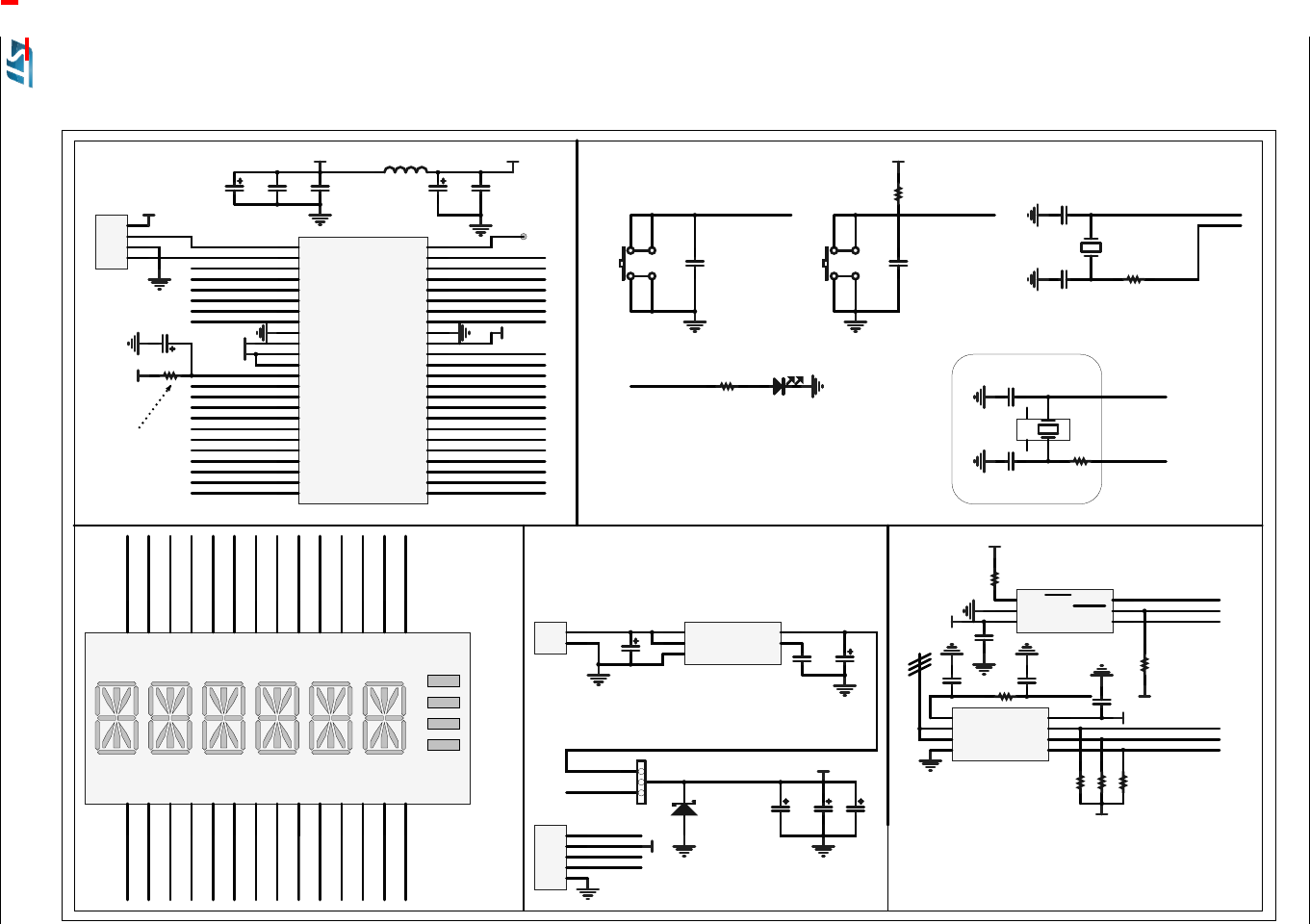
5 Electrical schematic diagrams
Figure 9. M24LR board schematics
/'
EOXH
5
%
5(6(7 %ODFN &
Q)
5(6(7
&
S)
&
S)
;
+& 6&66$
5
;
0& *4PDQXIDFWXUHU -)91<
&
S)
&
S)
&
Q)
9&&
&
Q)
/
%($' &
X) &
Q)
9&&$
&
X)
/('
%
86(5 %OXH &
Q)
5
5(6(7
5
.
9&&
8VHUB3%
&20
&20
&20
&20
8
*+7
$GGU7KHUP
*1'
9''
6&/
(9(17
6'$
8
6776:%)
&1
6:,0
&1
([WHUQDO '& 99
-3
=
006= %7 GR QRW ILW
/&'B&20
/&'B&20 /&'B&20
/&'B&20
/&'B6(*
/&'B6(*
/&'B6(*
/&'B6(*
/&'B6(*
/&'B6(*
/&'B6(*
/&'B6(*
/&'B6(*
/&'B6(*
/&'B6(*
/&'B6(* /&'B6(*
/&'B6(*
/&'B6(*
/&'B6(*
/&'B6(*
/&'B6(*
/&'B6(*
/&'B6(*
/&'B6(*
/&'B6(*
/&'B6(*
/&'B6(*
26&B,1
26&B287
26&B,1
26&B287
8VHU
9&&
&
Q)
5
.
5
.
5
.
9&&
,&B6'$
,&B6&/
5)B:, 3%86<
5)B32:(5
$QWHQQD
5)B32:(5
9&&
&
X)
9&&
9&&$
9&&
/('
3$
3$
3$
3$
3$
3$
3$
3$
$966
9''
9''$
95()
9/ &'
3(
3(
3(
3(
3(
3(
3'
3'
3'
3'
3%
3%
3%
3%
3%
3%
3%
3%
3)
3'
3'
3'
3'
3&
3&
9'', 2
966,2
3&
3&
3&
3&
3&
3&
3(
3(
8
670/ &7
5
9&&
1RW )LWWHG
/&'B&20
/&'B&20
/&'B&20
/&'B6(*
/&'B6(*
/&'B6(*
/&'B6(*
/&'B6(*
/&'B6(*
/&'B6(*
/&'B6(*
/&'B6(*
/&'B6(*
/&'B6(* /&'B6(*
/&'B6(*
/&'B6(*
/&'B6(*
/&'B6(*
/&'B6(*
/&'B6(*
/&'B6(*
/&'B6(*
/&'B6(*
/&'B6(*
/&'B6(*
/&'B6(*
/&'B&20
,&B6'$
,&B6&/
5)B:, 3%86<
7HP6HQVRUB717
26&B,1
26&B287
5(6(7
8VHUB3%
26&B,1
26&B287
5
.
9&&
,&B6&/
,&B6'$
7HP6HQVRUB717
&
Q)
9&&
5
.
9&&
1RW )LWWHG
9&&
9LQ
*1'
,1+, %, 7
%<3$66
9RXW
8
/'05
&
X)>FHUDPLF@
&
Q)
&
X)>FHUDPLF@
5(*B9
&
X)>FHUDPLF@
73
3(
9RXW
$&
$&
966
6'$
6&/
5) :, 3%86<
9&&
8
0/5( 5017
&
Q)
,&B6'$
,&B6&/ 9&&
,& FRQQHFWRU
5
&
>1$@
&1
+HDGHU
5)B:, 3%86<
&
7/ 1.05 X)
&
>1$@
Revision history UM1589
18/19 DocID023883 Rev 3
6 Revision history
Table 4. Document revision history
Date Revision Changes
06-Nov-2012 1Initial release.
11-Mar-2013 2
Replaced “M24LR/CR95HF demonstration software " by
"M24LR/CR95 application software setup file [STSW-M24LR011]" in
Section 1.1 and Section 3.4.
Replaced “M24LRxx_Application_Software.exe” by “setup.exe” in
Section 1.1.
dd-Feb-2015 3
Updated Figure 1: M24LR evaluation board andFigure 2: RF
transceiver demonstration board.
Added Section 4: Federal Communications Commission (FCC) and
Industry Canada (IC) Compliance Statements.

DocID023883 Rev 3 19/19
UM1589
19
IMPORTANT NOTICE – PLEASE READ CAREFULLY
STMicroelectronics NV and its subsidiaries (“ST”) reserve the right to make changes, corrections, enhancements, modifications, and
improvements to ST products and/or to this document at any time without notice. Purchasers should obtain the latest relevant information on
ST products before placing orders. ST products are sold pursuant to ST’s terms and conditions of sale in place at the time of order
acknowledgement.
Purchasers are solely responsible for the choice, selection, and use of ST products and ST assumes no liability for application assistance or
the design of Purchasers’ products.
No license, express or implied, to any intellectual property right is granted by ST herein.
Resale of ST products with provisions different from the information set forth herein shall void any warranty granted by ST for such product.
ST and the ST logo are trademarks of ST. All other product or service names are the property of their respective owners.
Information in this document supersedes and replaces information previously supplied in any prior versions of this document.
© 2015 STMicroelectronics – All rights reserved