STMicroelectronicsS R3911BD1 NFC card reader board User Manual Manual
STMicroelectronics NFC card reader board Manual
UserManual.wiki
>
STMicroelectronicsS
>
R3911BD1 User Manual
Manual
Navigation menu
Upload a User Manual
Namespaces
Wiki Guide
HTML
PDF
Info
Views
User Manual
Discussion / Help
Navigation
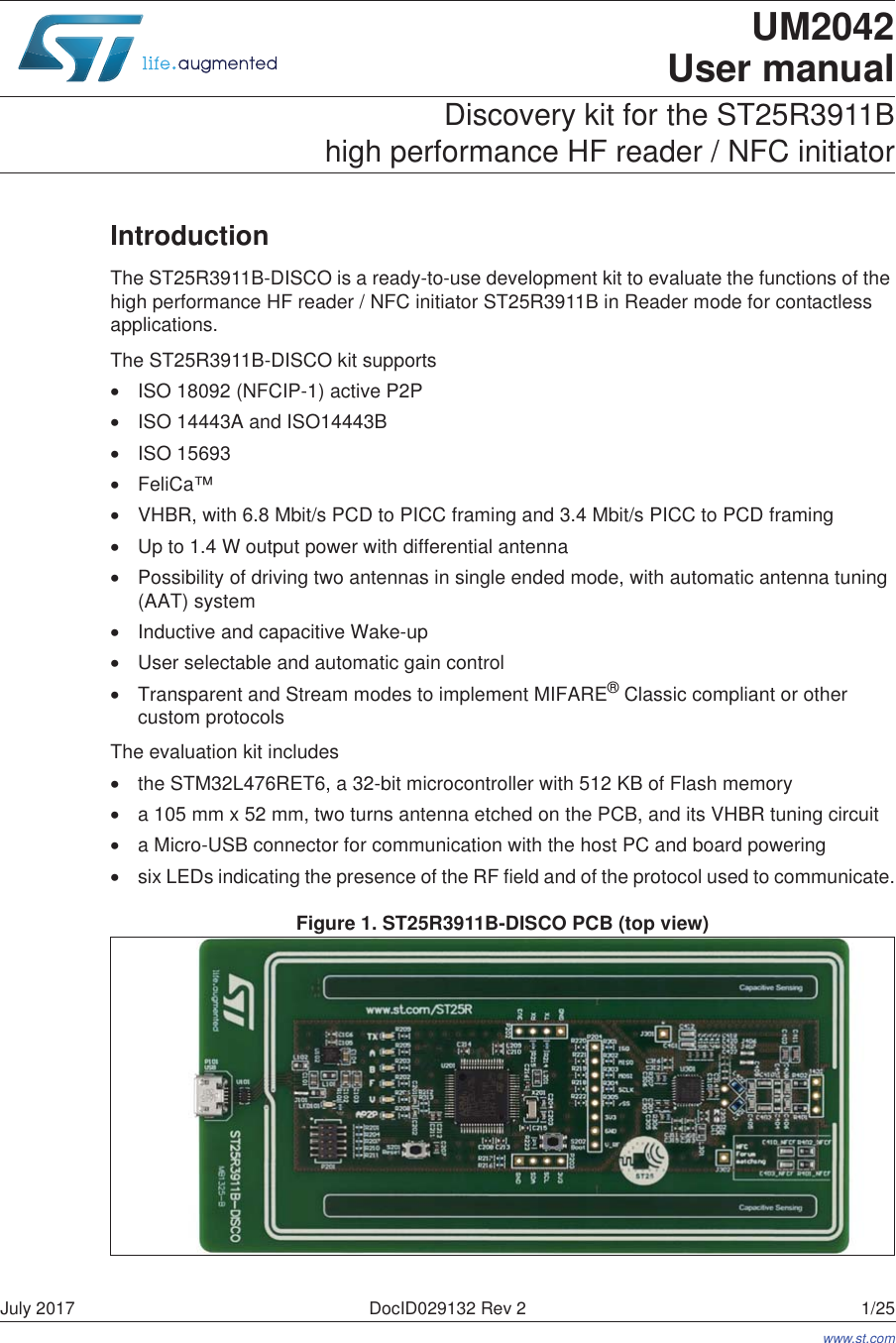
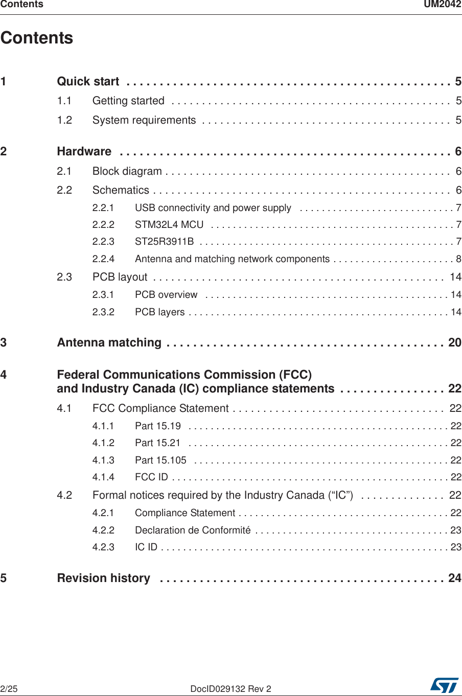
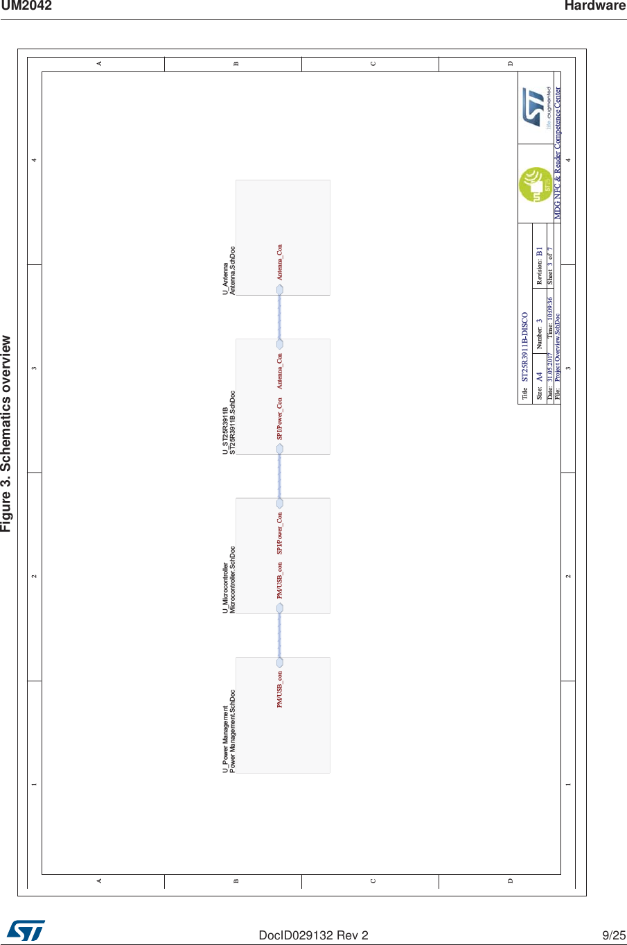
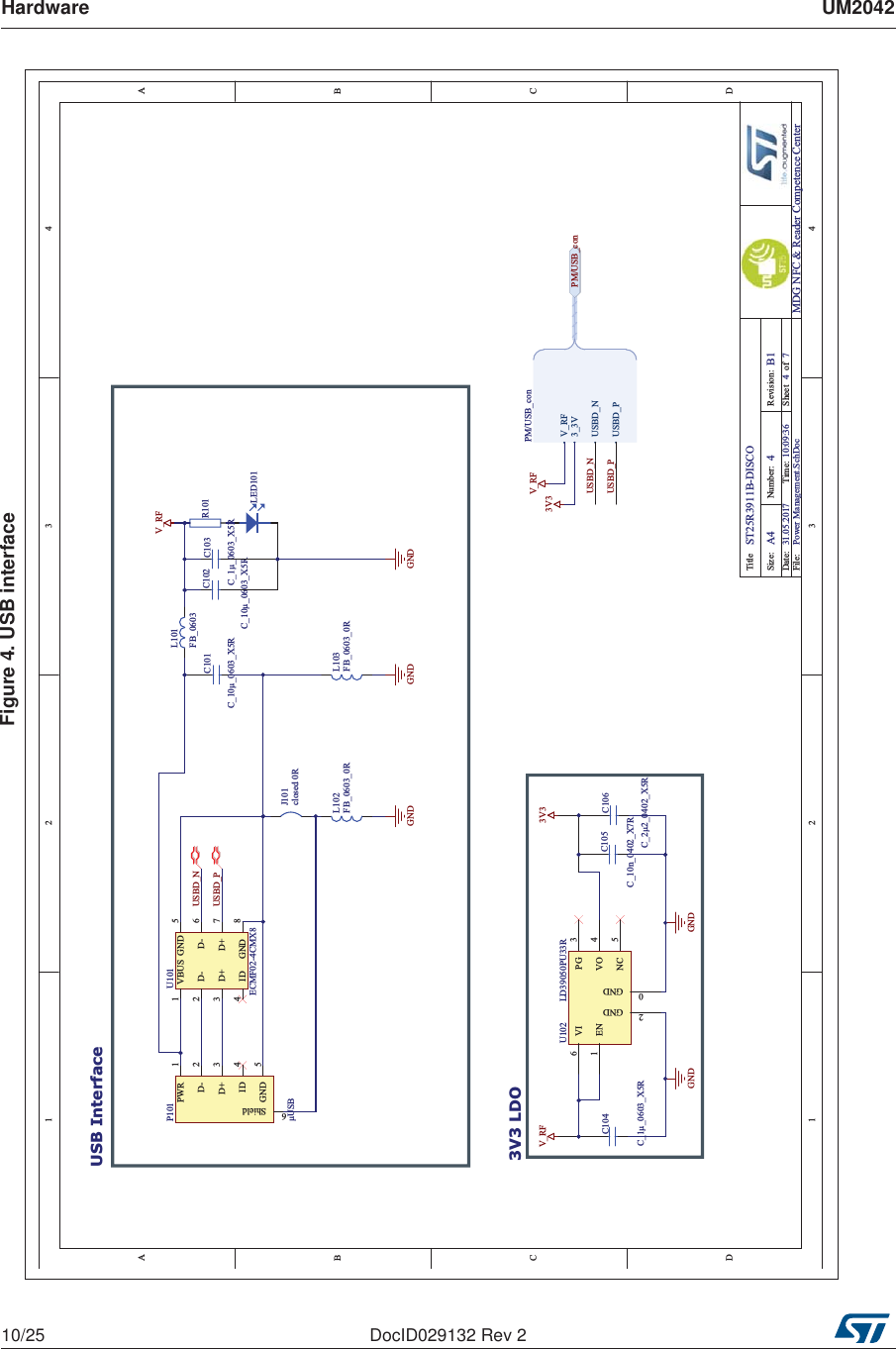
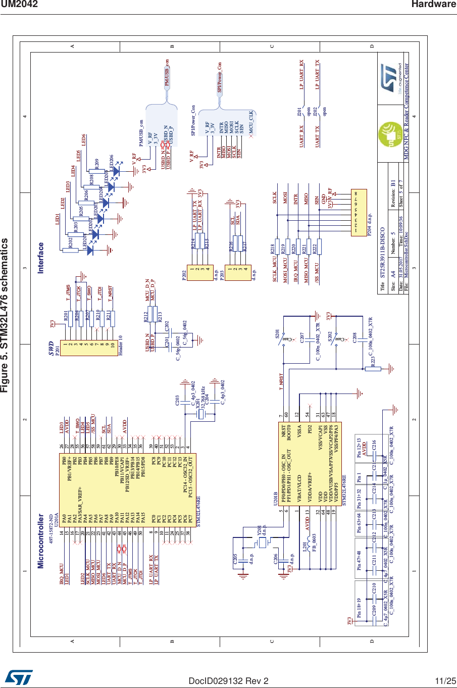
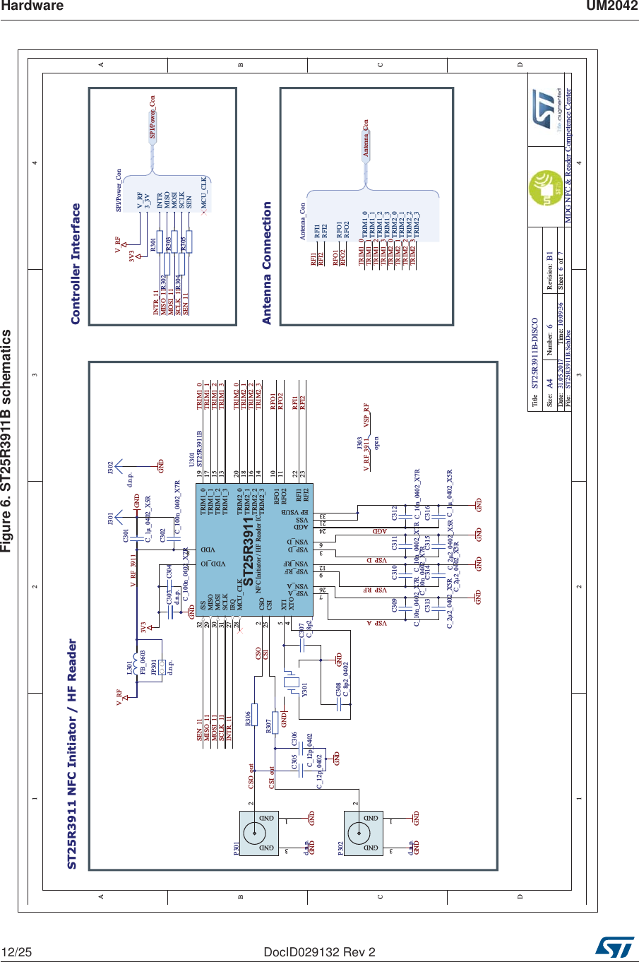
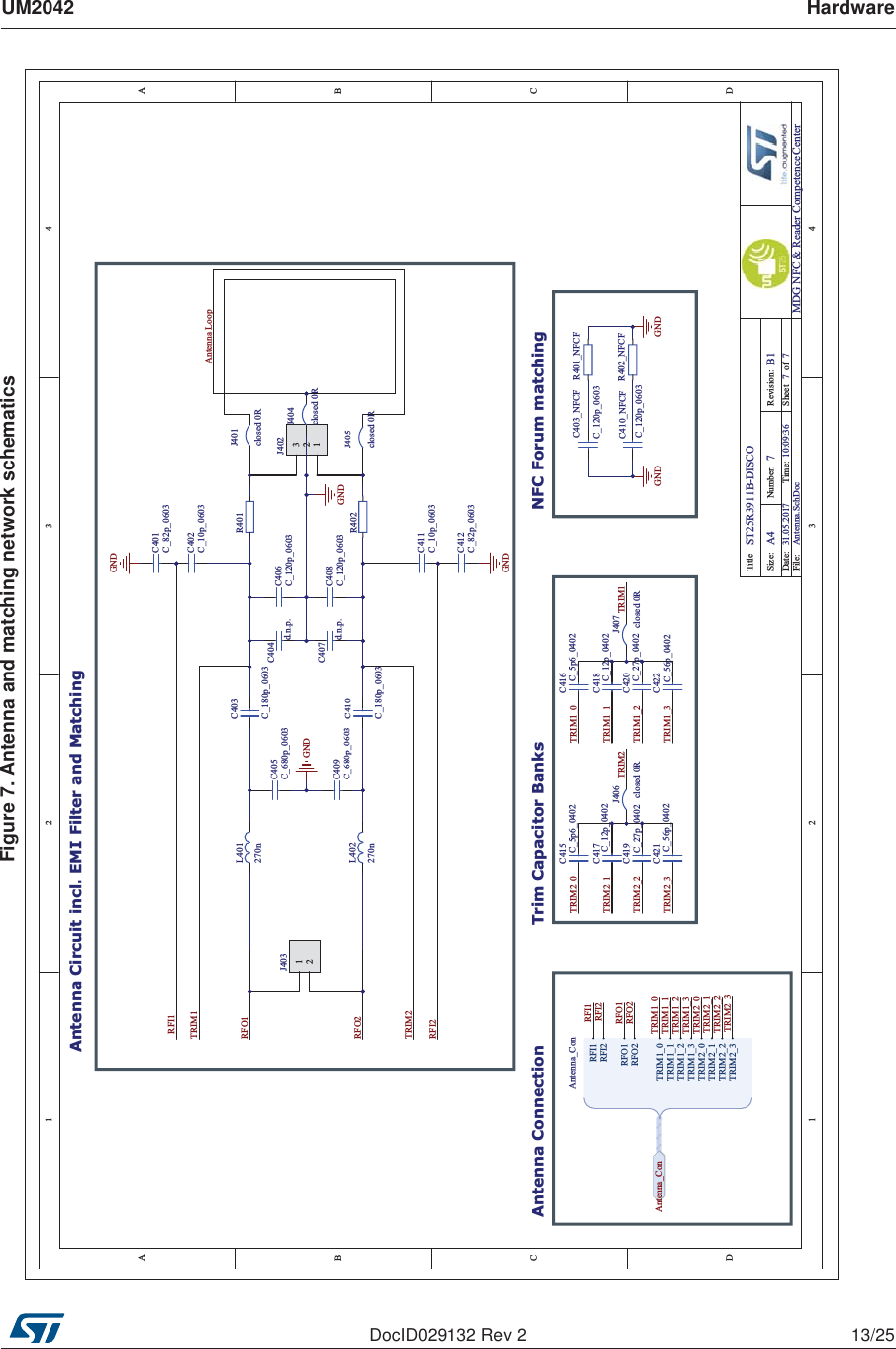
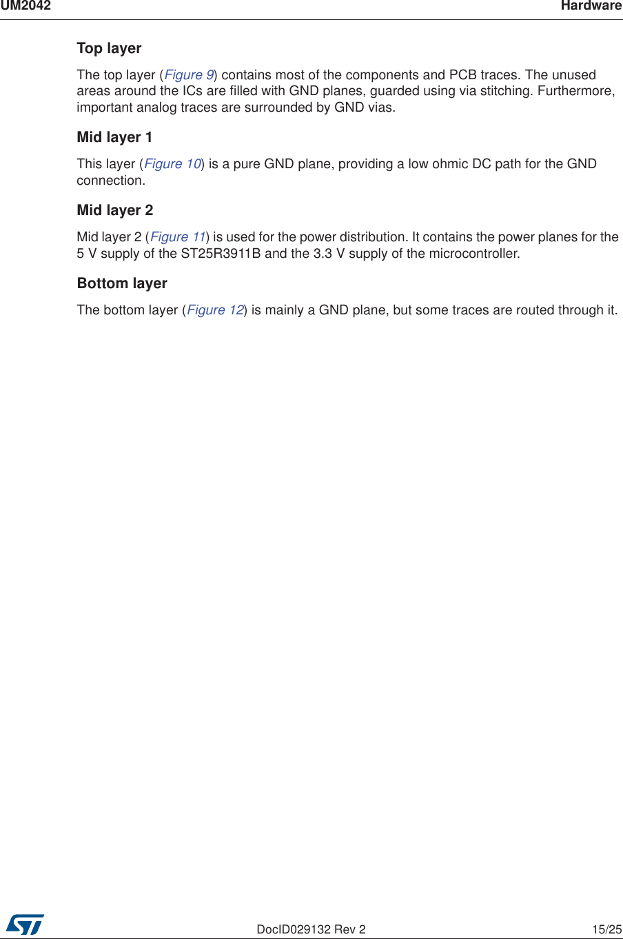
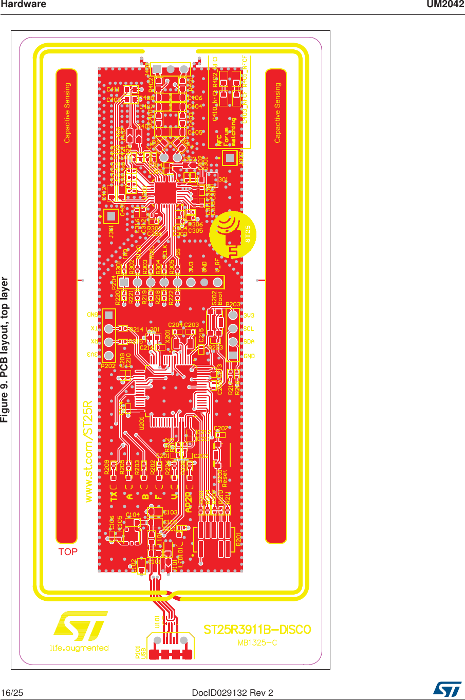
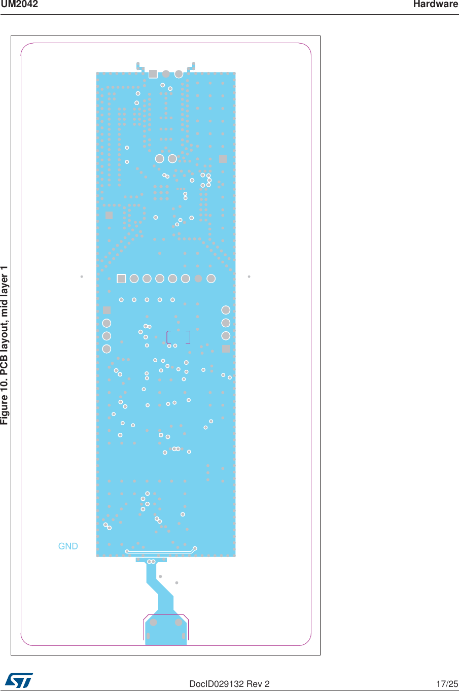
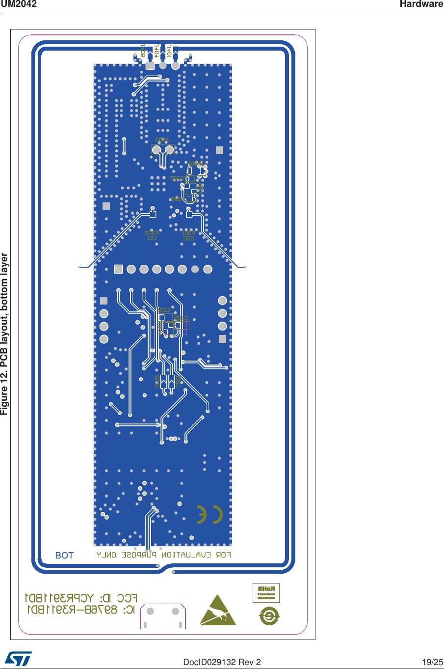
![Hardware UM20426/25 DocID029132 Rev 22 Hardware The PCB (Printed Circuit Board) is connected via USB to the PC. The STSW-ST25R001 PC software controls the STM32 MCU located on the PCB. The STM32 MCU then operates the ST25R3911B via SPI.The ST25R3911B is connected directly to the 5 V supply of the USB bus. An LDO converts this voltage down to 3.3 V, to supply the microcontroller.A green LED close to the USB plug indicates if the board is powered. Six blue LEDs indicate the mode of operation (transmit / receive) and which technologies are in use.The antenna runs along the PCB perimeter.2.1 Block diagramFigure 2 shows the functional block diagram of the board.Figure 2. Functional block diagram2.2 SchematicsAs indicated in Figure 3, the schematics can be split into four main parts•USB connectivity and power supply (Figure 4)•STM32 MCU (Figure 5)•ST25R3911B (Figure 6) •Antenna and matching network components (Figure 7)069+RVW3& (&0)&0;/'385N+]FU\VWDO0+]FU\VWDO670/5( 675% 3&%DQWHQQD63, 0DWFKLQJQHWZRUN9 986%675%',6&2](https://usermanual.wiki/STMicroelectronicsS/R3911BD1/User-Guide-3523975-Page-6.png)