STMicroelectronicsS R3911BD1 NFC card reader board User Manual Manual
STMicroelectronics NFC card reader board Manual
Manual
July 2017 DocID029132 Rev 2 1/25
1
UM2042
User manual
Discovery kit for the ST25R3911B
high performance HF reader / NFC initiator
Introduction
The ST25R3911B-DISCO is a ready-to-use development kit to evaluate the functions of the
high performance HF reader / NFC initiator ST25R3911B in Reader mode for contactless
applications.
The ST25R3911B-DISCO kit supports
•ISO 18092 (NFCIP-1) active P2P
•ISO 14443A and ISO14443B
•ISO 15693
•FeliCa™
•VHBR, with 6.8 Mbit/s PCD to PICC framing and 3.4 Mbit/s PICC to PCD framing
•Up to 1.4 W output power with differential antenna
•Possibility of driving two antennas in single ended mode, with automatic antenna tuning
(AAT) system
•Inductive and capacitive Wake-up
•User selectable and automatic gain control
•Transparent and Stream modes to implement MIFARE® Classic compliant or other
custom protocols
The evaluation kit includes
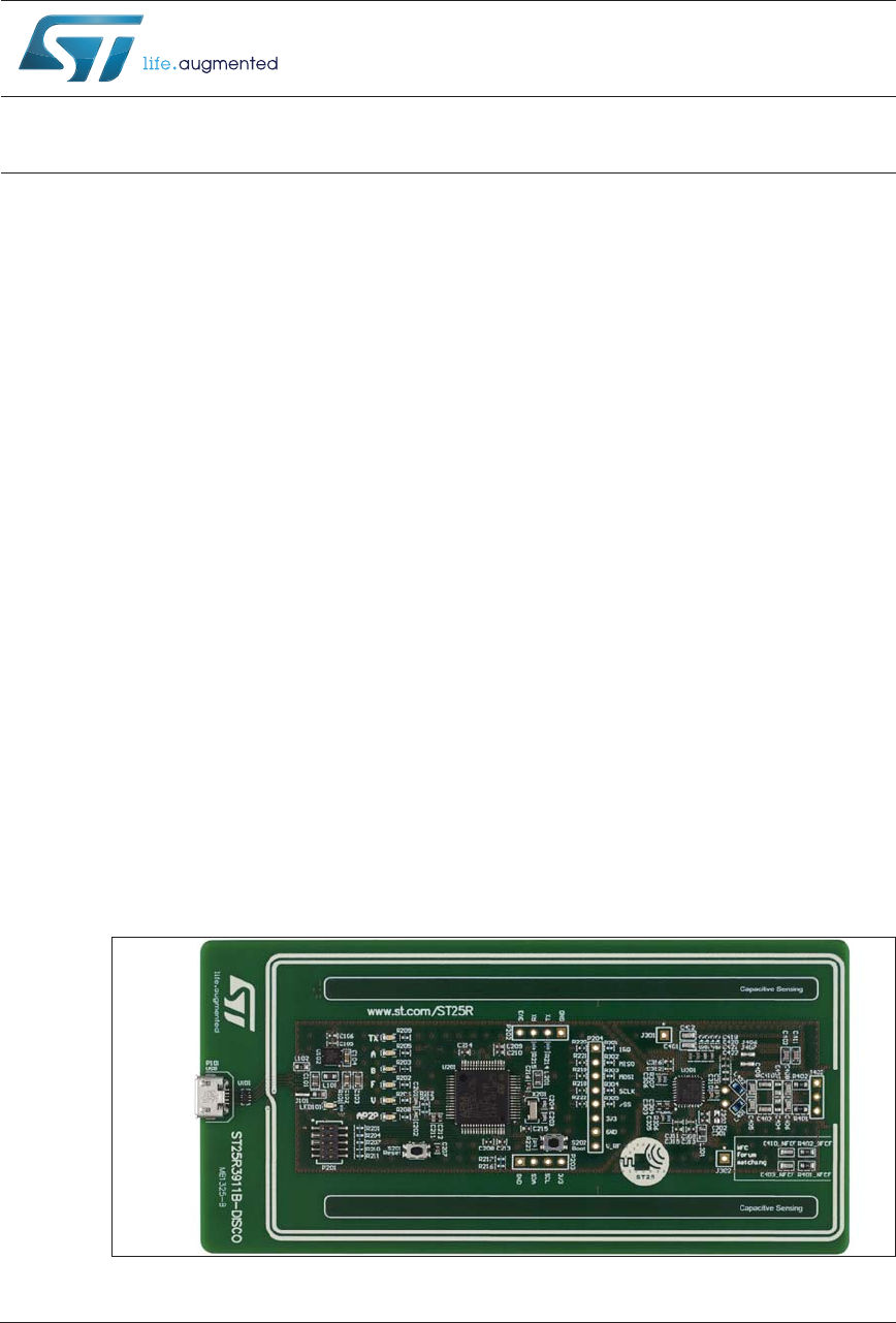
•the STM32L476RET6, a 32-bit microcontroller with 512 KB of Flash memory
•a 105 mm x 52 mm, two turns antenna etched on the PCB, and its VHBR tuning circuit
•a Micro-USB connector for communication with the host PC and board powering
•six LEDs indicating the presence of the RF field and of the protocol used to communicate.
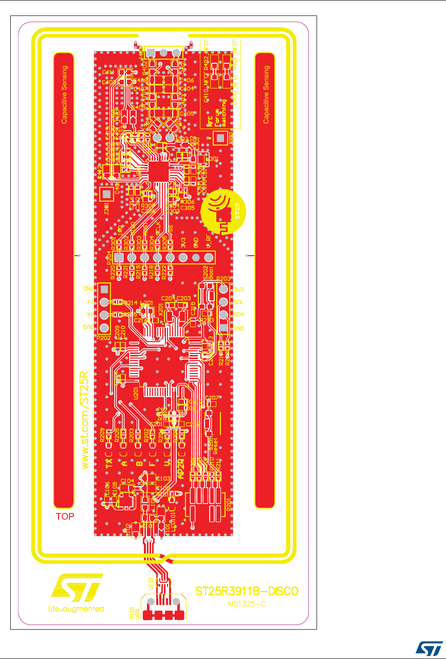
Figure 1. ST25R3911B-DISCO PCB (top view)
www.st.com

Contents UM2042
2/25 DocID029132 Rev 2
Contents
1 Quick start . . . . . . . . . . . . . . . . . . . . . . . . . . . . . . . . . . . . . . . . . . . . . . . . . 5
1.1 Getting started . . . . . . . . . . . . . . . . . . . . . . . . . . . . . . . . . . . . . . . . . . . . . . 5
1.2 System requirements . . . . . . . . . . . . . . . . . . . . . . . . . . . . . . . . . . . . . . . . . 5
2 Hardware . . . . . . . . . . . . . . . . . . . . . . . . . . . . . . . . . . . . . . . . . . . . . . . . . . 6
2.1 Block diagram . . . . . . . . . . . . . . . . . . . . . . . . . . . . . . . . . . . . . . . . . . . . . . . 6
2.2 Schematics . . . . . . . . . . . . . . . . . . . . . . . . . . . . . . . . . . . . . . . . . . . . . . . . . 6
2.2.1 USB connectivity and power supply . . . . . . . . . . . . . . . . . . . . . . . . . . . . 7
2.2.2 STM32L4 MCU . . . . . . . . . . . . . . . . . . . . . . . . . . . . . . . . . . . . . . . . . . . . 7
2.2.3 ST25R3911B . . . . . . . . . . . . . . . . . . . . . . . . . . . . . . . . . . . . . . . . . . . . . . 7
2.2.4 Antenna and matching network components . . . . . . . . . . . . . . . . . . . . . . 8
2.3 PCB layout . . . . . . . . . . . . . . . . . . . . . . . . . . . . . . . . . . . . . . . . . . . . . . . . 14
2.3.1 PCB overview . . . . . . . . . . . . . . . . . . . . . . . . . . . . . . . . . . . . . . . . . . . . 14
2.3.2 PCB layers . . . . . . . . . . . . . . . . . . . . . . . . . . . . . . . . . . . . . . . . . . . . . . . 14
3 Antenna matching . . . . . . . . . . . . . . . . . . . . . . . . . . . . . . . . . . . . . . . . . . 20
4 Federal Communications Commission (FCC)
and Industry Canada (IC) compliance statements . . . . . . . . . . . . . . . . 22
4.1 FCC Compliance Statement . . . . . . . . . . . . . . . . . . . . . . . . . . . . . . . . . . . 22
4.1.1 Part 15.19 . . . . . . . . . . . . . . . . . . . . . . . . . . . . . . . . . . . . . . . . . . . . . . . 22
4.1.2 Part 15.21 . . . . . . . . . . . . . . . . . . . . . . . . . . . . . . . . . . . . . . . . . . . . . . . 22
4.1.3 Part 15.105 . . . . . . . . . . . . . . . . . . . . . . . . . . . . . . . . . . . . . . . . . . . . . . 22
4.1.4 FCC ID . . . . . . . . . . . . . . . . . . . . . . . . . . . . . . . . . . . . . . . . . . . . . . . . . . 22
4.2 Formal notices required by the Industry Canada (“IC”) . . . . . . . . . . . . . . 22
4.2.1 Compliance Statement . . . . . . . . . . . . . . . . . . . . . . . . . . . . . . . . . . . . . . 22
4.2.2 Declaration de Conformité . . . . . . . . . . . . . . . . . . . . . . . . . . . . . . . . . . . 23
4.2.3 IC ID . . . . . . . . . . . . . . . . . . . . . . . . . . . . . . . . . . . . . . . . . . . . . . . . . . . . 23
5 Revision history . . . . . . . . . . . . . . . . . . . . . . . . . . . . . . . . . . . . . . . . . . . 24

DocID029132 Rev 2 3/25
UM2042 List of tables
3
List of tables
Table 1. NFC Forum matching alternatives . . . . . . . . . . . . . . . . . . . . . . . . . . . . . . . . . . . . . . . . . . . 21
Table 2. Document revision history . . . . . . . . . . . . . . . . . . . . . . . . . . . . . . . . . . . . . . . . . . . . . . . . . 24

List of figures UM2042
4/25 DocID029132 Rev 2
List of figures
Figure 1. ST25R3911B-DISCO PCB (top view). . . . . . . . . . . . . . . . . . . . . . . . . . . . . . . . . . . . . . . . . . 1
Figure 2. Functional block diagram . . . . . . . . . . . . . . . . . . . . . . . . . . . . . . . . . . . . . . . . . . . . . . . . . . . 6
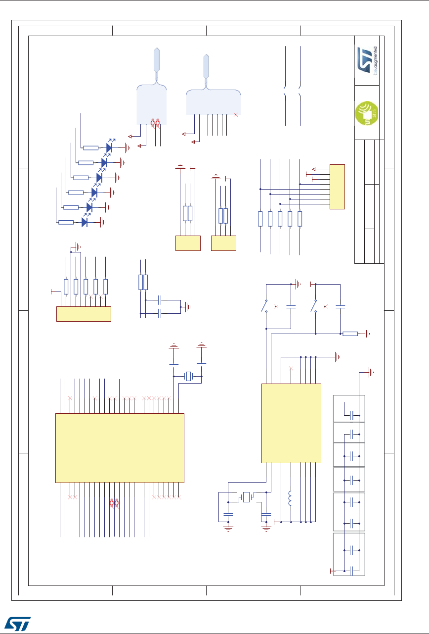
Figure 3. Schematics overview . . . . . . . . . . . . . . . . . . . . . . . . . . . . . . . . . . . . . . . . . . . . . . . . . . . . . . 9
Figure 4. USB interface . . . . . . . . . . . . . . . . . . . . . . . . . . . . . . . . . . . . . . . . . . . . . . . . . . . . . . . . . . . 10
Figure 5. STM32L476 schematics . . . . . . . . . . . . . . . . . . . . . . . . . . . . . . . . . . . . . . . . . . . . . . . . . . . 11
Figure 6. ST25R3911B schematics . . . . . . . . . . . . . . . . . . . . . . . . . . . . . . . . . . . . . . . . . . . . . . . . . . 12
Figure 7. Antenna and matching network schematics . . . . . . . . . . . . . . . . . . . . . . . . . . . . . . . . . . . . 13
Figure 8. PCB overview . . . . . . . . . . . . . . . . . . . . . . . . . . . . . . . . . . . . . . . . . . . . . . . . . . . . . . . . . . . 14
Figure 9. PCB layout, top layer . . . . . . . . . . . . . . . . . . . . . . . . . . . . . . . . . . . . . . . . . . . . . . . . . . . . . 16
Figure 10. PCB layout, mid layer 1 . . . . . . . . . . . . . . . . . . . . . . . . . . . . . . . . . . . . . . . . . . . . . . . . . . . 17
Figure 11. PCB layout, mid layer 2 . . . . . . . . . . . . . . . . . . . . . . . . . . . . . . . . . . . . . . . . . . . . . . . . . . . 18
Figure 12. PCB layout, bottom layer . . . . . . . . . . . . . . . . . . . . . . . . . . . . . . . . . . . . . . . . . . . . . . . . . . 19
Figure 13. VHBR matching with an AAT setting of 8 . . . . . . . . . . . . . . . . . . . . . . . . . . . . . . . . . . . . . . 20
Figure 14. NFC Forum matching with an AAT setting of 11 . . . . . . . . . . . . . . . . . . . . . . . . . . . . . . . . 21

DocID029132 Rev 2 5/25
UM2042 Quick start
24
1 Quick start
The ST25R3911B-DISCO is connected to a PC via USB to show the features of the
ST25R3911B chip. To do so, use the software STSW-ST25R001 to control all the functions
of the discovery kit.
1.1 Getting started
Connect the discovery kit to a PC using a micro USB cable. The USB port of the PC must be
capable of delivering at least 250 mA at 5 Volt supply.
To control the board, download the software STSW-ST25R001 from www.st.com and install
it. Further information on how to operate the software can be found in the user manual
UM2177 “PC software for the ST25R3911B-DISCO kit”, available on www.st.com.
1.2 System requirements
•Windows® PC (Windows 7 recommended)
•USB port, capable of delivering at least 250 mA at 5 V supply (1.25 W)
•Unit must be supplied by a Safety Extra Low Voltage (SELV) limited power source
through the USB port, the source should not exceed 60 Vdc / 8 A / 100 VA
•Micro-USB cable
Hardware UM2042
6/25 DocID029132 Rev 2
2 Hardware
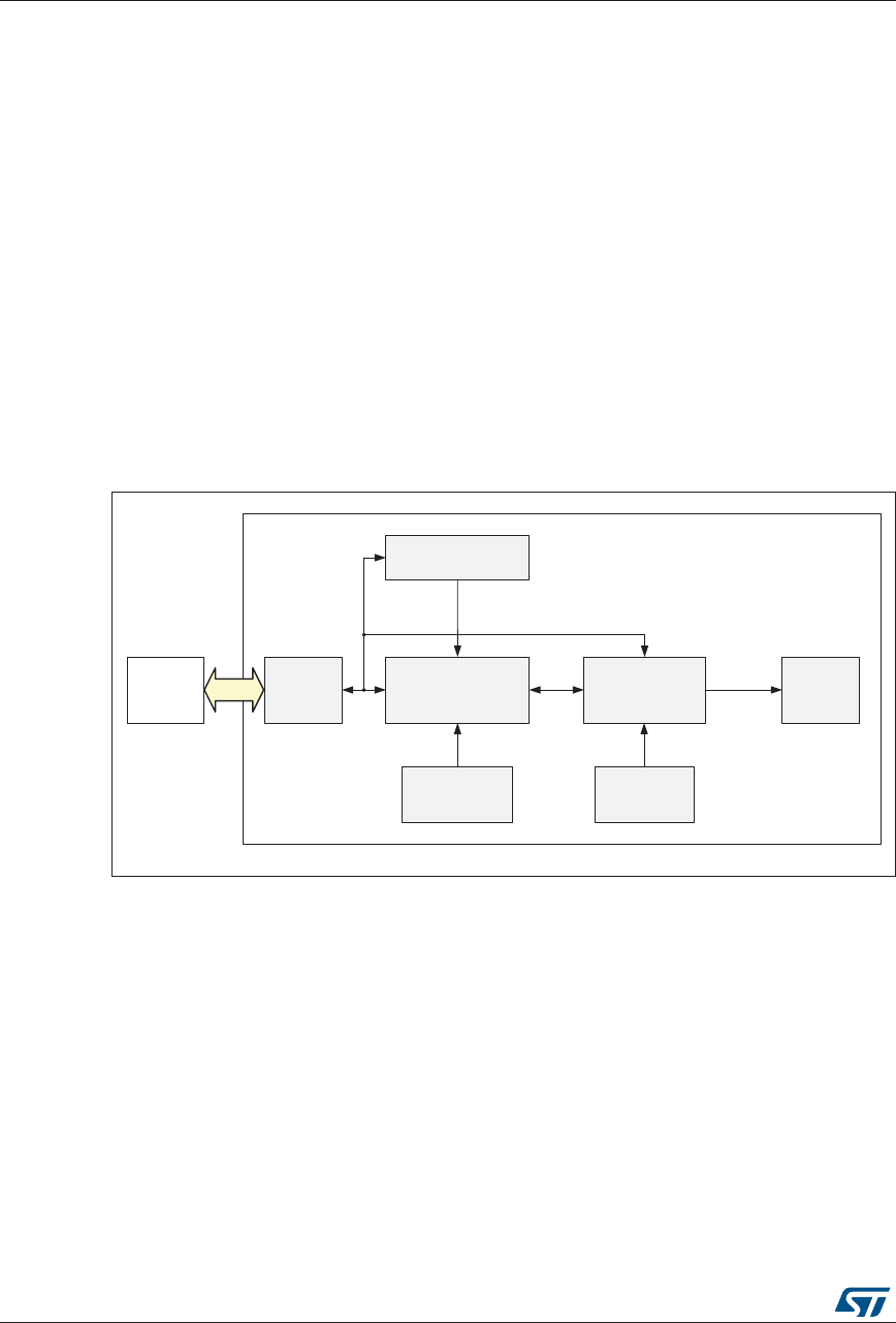
The PCB (Printed Circuit Board) is connected via USB to the PC. The STSW-ST25R001 PC
software controls the STM32 MCU located on the PCB. The STM32 MCU then operates the
ST25R3911B via SPI.
The ST25R3911B is connected directly to the 5 V supply of the USB bus. An LDO converts
this voltage down to 3.3 V, to supply the microcontroller.
A green LED close to the USB plug indicates if the board is powered. Six blue LEDs indicate
the mode of operation (transmit / receive) and which technologies are in use.
The antenna runs along the PCB perimeter.
2.1 Block diagram
Figure 2 shows the functional block diagram of the board.
Figure 2. Functional block diagram
2.2 Schematics
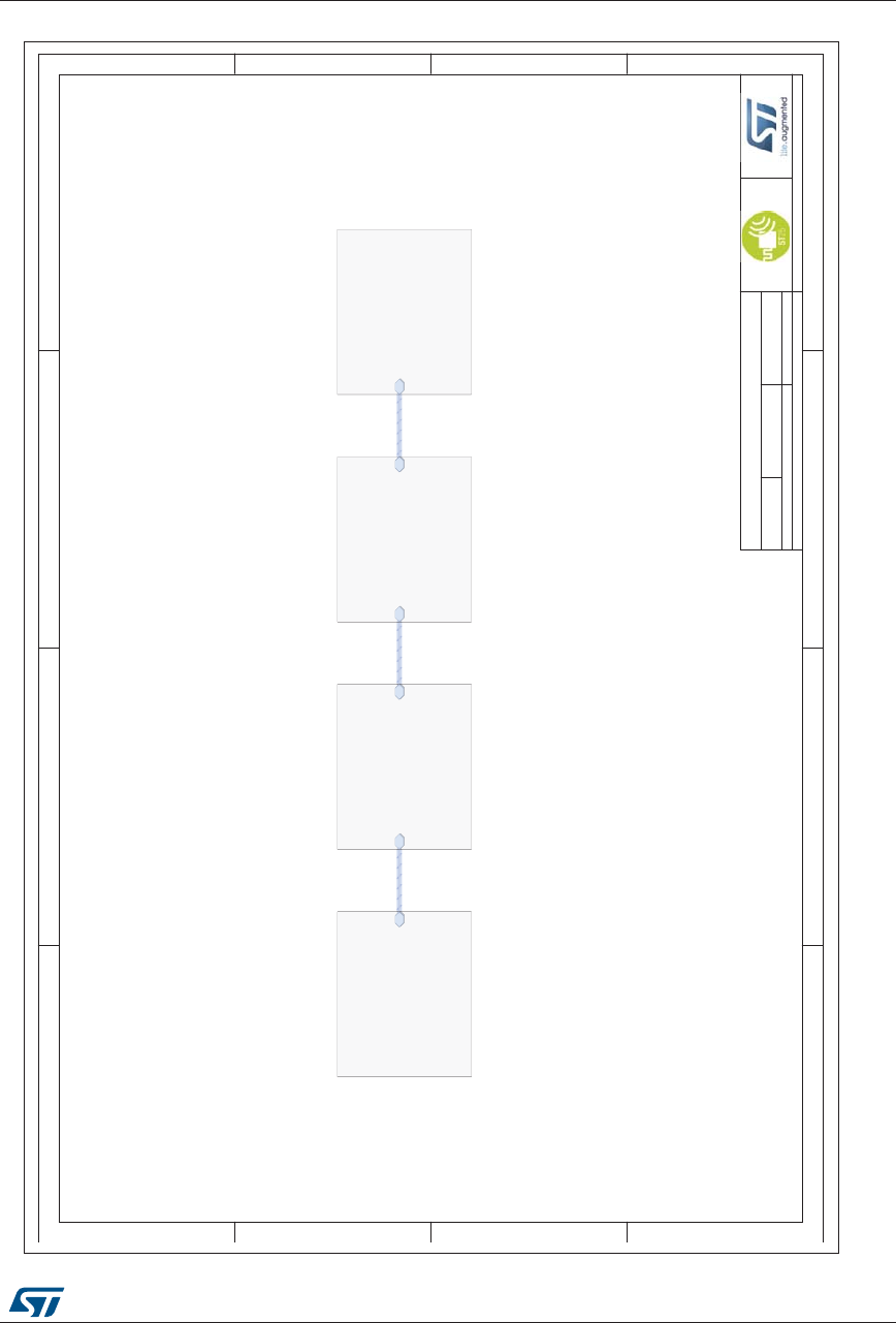
As indicated in Figure 3, the schematics can be split into four main parts
•USB connectivity and power supply (Figure 4)
•STM32 MCU (Figure 5)
•ST25R3911B (Figure 6)
•Antenna and matching network components (Figure 7)
069
+RVW3& (&0)
&0;
/'385
N+]
FU\VWDO
0+]
FU\VWDO
670/5( 675% 3&%
DQWHQQD
63, 0DWFKLQJ
QHWZRUN
9 9
86%
675%',6&2

DocID029132 Rev 2 7/25
UM2042 Hardware
24
2.2.1 USB connectivity and power supply
The ST25R3911B-DISCO board can be connected via USB to a host device.
Right behind the Micro-USB plug, an ECMF02 common mode filter with ESD protection for
USB 2.0 interface is placed. The common mode filter is connected to VBUS and to the
D+/D- data lines of the USB. All the USB terminals are ESD-protected by the built-in ESD
diodes of the ECMF02.
Additionally, the power supply filter for the 5 V supplies the 3.3 V LDO, that, in turn, supplies
the microcontroller.
A green LED is connected to the USB VBUS supply and shows the USB-power status.
2.2.2 STM32L4 MCU
This schematic includes the microcontroller needed to operate the NFC reader IC.
The MCU is clocked by a 32.768 kHz crystal. The MCU uses an internal PLL to generate the
48 MHz USB clock and the 80 MHz core clock from the provided 32.768 kHz.
Connector P201 is a JTAG/SWD interface to assist in software development. It can be
connected to an external ST-LINK/V2 device using a 9-pin Cortex®-M adapter.
The six blue LEDs (LED201 to LED206) show the current mode of communication. If
multiple protocols are active at the same time, then all corresponding LEDs are turned on.
The five resistors (R218 to R222) can be used to disconnect the MCU from SPI interface
header P204. This SPI cross-connect mode can be used to operate the ST25R3911B with a
different MCU PCB by cross connecting the ST25R3911B SPI to the second MCU PCB.
Connectors P202 and P203 can be used to connect an external UART or I2C host device to
the MCU.
2.2.3 ST25R3911B
The ST25R3911B is directly connected to the filtered 5 V USB supply, and there are
additional supply filtering components placed close to it. The jumper JP301 can be used to
measure the supply current of the chip. If this measurement is performed, the ferrite bead
L301 has to be removed.
Capacitors C301 to C304 provide additional filtering. All decoupling capacitors have been
placed as close as possible to the ST25R3911B. Special care has been taken for C310,
C302, C314 and C301, as they are the decoupling capacitors for the high power driver
stage.
In order to demonstrate the capacitive wake-up feature, two capacitive electrodes are
placed on the PCB. Additional electrodes can be connected using UFL connectors on P301
and P302.
For SPI cross-connecting to another reader PCB, the resistors R301 to R305 can be
removed. Then the STM32L4 MCU SPI can be connected to the ST25R3911B on any
customer PCB via header P204.
Thanks to J303 it is possible to bypass the internal VSP_RF regulator, this is required in
case output currents higher than 200 mA need to be supplied.

Hardware UM2042
8/25 DocID029132 Rev 2
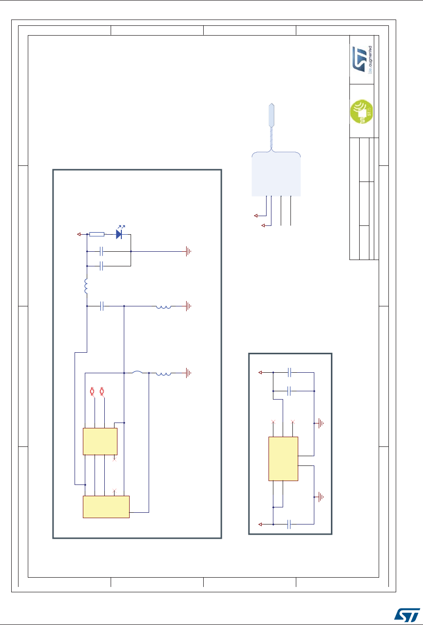
2.2.4 Antenna and matching network components
This schematic contains the matching network and the automatic antenna tuning capacitors,
as well as the alternative NFC Forum matching components. In the default configuration,
the ST25R3911B-DISCO is populated with a VHBR matching, with communication speeds
up to 3.4 Mbps.
To support VHBR, the antenna is matched to a system Q-Factor of 8. By switching to the
NFC Forum matching components the system Q-Factor is increased to 16. This can
increase the read range up to 20%, depending on the used communication technology, but
limits the maximum supported communication bit rate to 848 kbps. Additional details about
antenna matching can be found on www.st.com/st25r.
UM2042 Hardware
DocID029132 Rev 2 9/25
Figure 3. Schematics overview
1
1
2
2
3
3
4
4
D D
C C
B B
A A
37
3B1
31.05.2017 10:09:36
Project Overview.SchDoc
Title
Size: Number:
Date:
File:
Revision:
Sheet of
Time:
A4
ST25R3911B-DISCO
MDG NFC & Reader Competence Center
PM/USB_con
U_Power Management
Power Management.SchDoc
Antenna_Con
U_Antenna
Antenna.SchDoc
SPI/Power_ConPM/USB_con
U_Microcontroller
Microcontroller.SchDoc
Antenna_ConSPI/Power_Con
U_ST25R3911B
ST25R3911B.SchDoc
Hardware UM2042
10/25 DocID029132 Rev 2
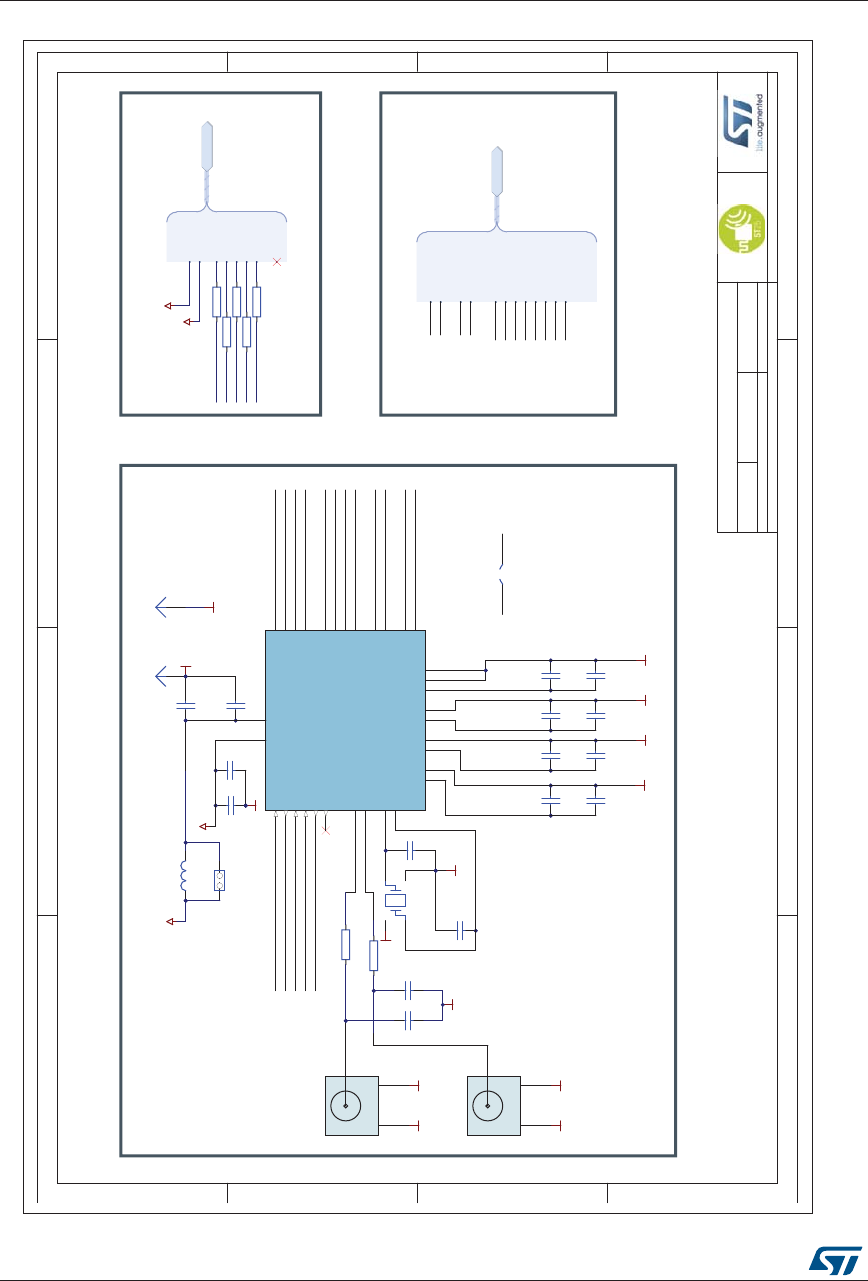
Figure 4. USB interface
1
1
2
2
3
3
4
4
D D
C C
B B
A A
47
4B1
31.05.2017 10:09:36
Power Management.SchDoc
Title
Size: Number:
Date:
File:
Revision:
Sheet of
Time:
A4
ST25R3911B-DISCO
MDG NFC & Reader Competence Center
3V3
GND
3V3 LDO
GNDGND
USB Interface
USBD_P
USBD_N
V_RF
3_3V
PM/USB_con
GND
EN
1
GND
2
VO 4
NC 5
GND
0
VI
6PG 3
U102 LD39050PU33R
GND
ESD
G101
Logo_ESD
RoHS
G102
Logo_RoHS
ST25
G103
Logo_ST25
ST Microelectronics
G104
Logo_STM
L102
FB_0603_0R
L101
FB_0603
C104
C_1μ_0603_X5R
C103
C_1μ_0603_X5R
C106
C_2μ2_0402_X5R
C105
C_10n_0402_X7R
C102
C_10μ_0603_X5R
C101
C_10μ_0603_X5R
R101
LED101
PWR 1
D- 2
D+ 3
ID 4
Shield
6
GND 5
P101
μUSB
VBUS
1
D-
2
D+
3
ID
4
GND 5
D- 6
D+ 7
GND 8
U101
ECMF02-4CMX8
V_RF
V_RF
V_RF
3V3
J101
closed 0R
L103
FB_0603_0R
PM/USB_con
USBD_N
USBD_P
USBD_P
USBD_N
UM2042 Hardware
DocID029132 Rev 2 11/25
Figure 5. STM32L476 schematics
1
1
2
2
3
3
4
4
D D
C C
B B
A A
57
5B1
31.05.2017 10:09:36
Microcontroller.SchDoc
Title
Size: Number:
Date:
File:
Revision:
Sheet of
Time:
A4
ST25R3911B-DISCO
MDG NFC & Reader Competence Center
Microcontroller
SEN
INTR
MISO
MOSI
SCLK
MCU_CLK
V_RF
3_3V
SPI/Power_Con
SPI/Power_Con
USBD_N
USBD_P
V_RF
3_3V
PM/USB_con
PM/USB_con
Interface
LP_UART_RX
LP_UART_TXUART_TX
UART_RX
3V3
GND
1
2
3
4
5
6
7
8
P204 d.n.p.
SWD
3V3
PC13 2
PC14 - OSC32_IN 3
PC15 - OSC32_OUT 4
PC0
8
PC1
9
PC2
10
PC3
11
PA0
14
PA1
15
PA2
16
PA3/SAR_VREF+
17
PA4
20
PA5
21
PA6
22
PA7
23
PC4
24
PC5
25
PB0 26
PB1/VREF+ 27
PB2 28
PB10/PE8 29
PB11/VCAP1 30
PB12/SD_VREF+ 33
PB13/PB14 34
PB14/PB15 35
PB15/PD8 36
PC6
37
PC7
38
PC8 39
PC9 40
PA8
41
PA9
42
PA10
43
PA11
44
PA12
45
PA13
46
PA14
49
PA15
50
PC10 51
PC11 52
PC12 53
PB3 55
PB4 56
PB5 57
PB6 58
PB7 59
PB8 61
PB9 62
497-15872-ND
U201A
STM32L476RE
SCLK_MCU
MISO_MCU
MOSI_MCU
LP_UART_RX
LP_UART_TX
UART_TX
UART_RX
IRQ_MCU
LED1
LED2
VBAT/VLCD
1
PF0/PD0/PH0 - OSC_IN
5
PF1/PD1/PH1 - OSC_OUT
6NRST 7
VSSA 12
VDDA/VREF+
13
VSS/PF4/PA3 18
VDD/PF5
19
VSS/VCAP1 31
VDD
32
VSS/VCAP2/PF6 47
VDD/VUSB/VSA/PF7
48
BOOT0 60
VSS 63
VDD
64
PD2 54
U201B
STM32L476RE
3V3
T_NRST
Case
S201
Case
S202 3V3
1
2
3
4
P203
d.n.p.
3V3
1
2
3
4
P202
d.n.p.
LP_UART_RX
LP_UART_TX
T_NRST
T_JTDI
T_SWO
T_JTCK
T_JTMS
LED1
LED2
LED3
LED4
LED5
LED6
SEN
MISO
INTR
MOSI
SCLKSCLK_MCU
MOSI_MCU
IRQ_MCU
MISO_MCU
/SS_MCU
SDA
SCL
3V3
C206
d.n.p.
C205
d.n.p.
Y201
d.n.p.
USBD_N
USBD_P
J201
open
J202
open
Pin 18+19 Pin 47+48 Pin 63+64 Pin 12+13Pin 31+32 Pin 1
3V3
Pin 18+
19
Pin 47+
48
P
in 63+
6
4Pin 31+
32
Pin 1
V_RF
3V3
R202
R203
R205
R206
R208
R209
R201
R204
R207
R210
R211
R214
R215
R216
R217
R218
R219
R220
R221
R222
C203
C_4p3_0402
C204
C_4p3_0402
X201
32.768 kHz
1
2
3
4
5
6
7
8
9
10
P201
Header 10
C209
C_4μ7_0402_X5R
C211
C_4μ7_0402_X5R
C210
C_100n_0402_X7R
C212
C_100n_0402_X7R
C213
C_100n_0402_X7R
C214
C_100n_0402_X7R
C216
C_100n_0402_X7R
C215
C_1μ_0402_X5R
C207
C_100n_0402_X7R
C208
C_100n_0402_X7R
R223
L201
FB_0603
AVDD
AVDD
LED201
LED202
LED203
LED204
LED205
LED206
INTR
MISO
MOSI
SCLK
SEN
V_RF
3V3
V_RF
LED6
C201
C_56p_0402
C202
C_56p_0402
R212
R213
USBD_P
USBD_N MCU_D_N
MCU_D_P
T_JTMS
T_JTCK
T_JTDI
MCU_D_P
MCU_D_N
AVDD
SDA
SCL
/SS_MCU
LED5
LED4
T_SWO
AVDD
LED3
P
in 12+
13
C21
6
5
5
5
X
5R
A
V
DD
5
X
Hardware UM2042
12/25 DocID029132 Rev 2
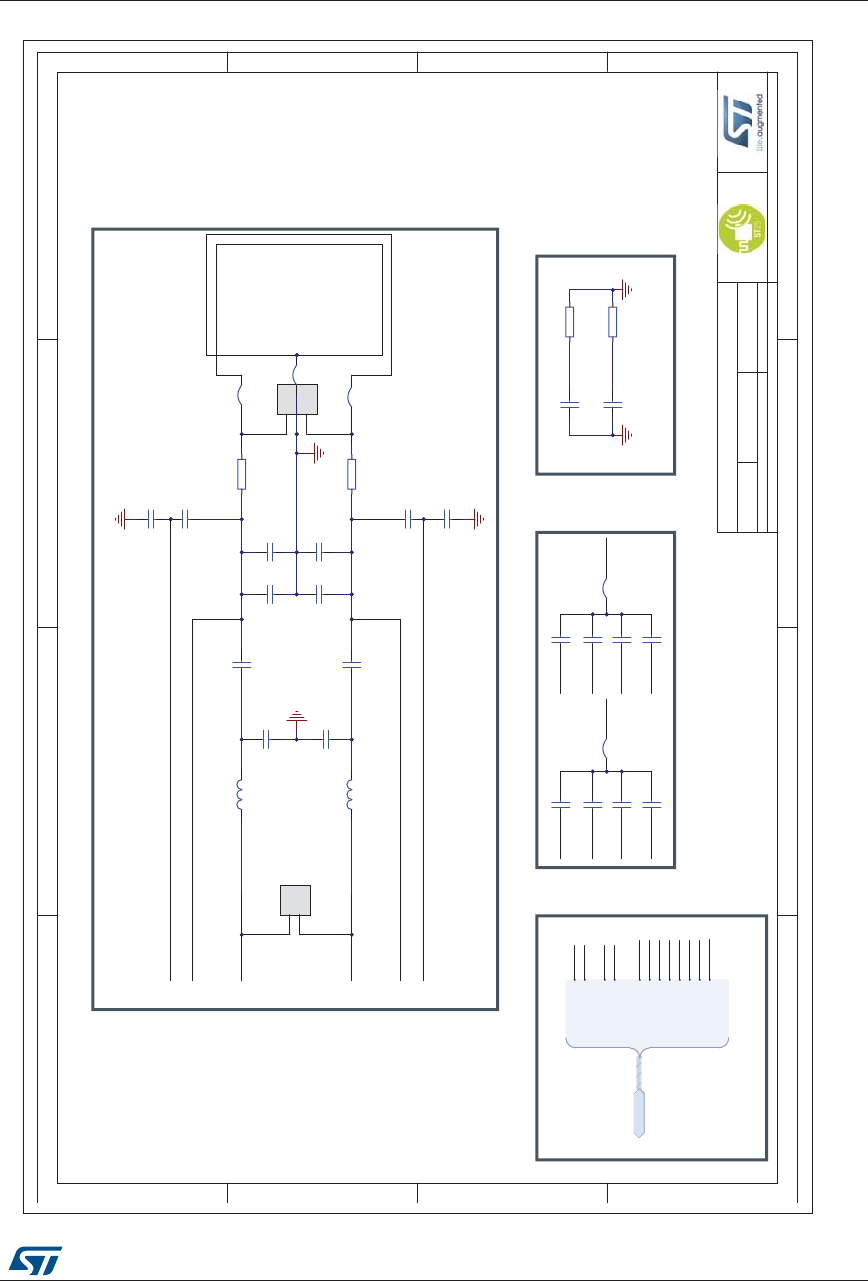
Figure 6. ST25R3911B schematics
1
1
2
2
3
3
4
4
D D
C C
B B
A A
67
6B1
31.05.2017 10:09:36
ST25R3911B.SchDoc
Title
Size: Number:
Date:
File:
Revision:
Sheet of
Time:
A4
ST25R3911B-DISCO
MDG NFC & Reader Competence Center
GND
GND
GND
GND
CSO
CSI
TRIM1_0
TRIM1_1
TRIM1_2
TRIM1_3
TRIM2_0
TRIM2_1
TRIM2_2
TRIM2_3
RFO1
RFO2
RFI1
RFI2
SEN_11
MISO_11
MOSI_11
SCLK_11
INTR_11
VSP_RF
VSP_RF
J301
C303
d.n.p.
GND
CSO_out
GND GND
GNDGND
GND
1
GND
3
2
P301
d.n.p.
GND
1
GND
3
2
P302
d.n.p.
V_RF_3911
RFI1
RFI2
RFO1
RFO2
TRIM1_0
TRIM1_1
TRIM1_2
TRIM1_3
TRIM2_0
TRIM2_1
TRIM2_2
TRIM2_3
Antenna_Con
Antenna_Con
TRIM2_0
TRIM2_1
TRIM2_2
TRIM2_3
TRIM1_0
TRIM1_1
TRIM1_2
TRIM1_3
RFO1
RFO2
RFI2
RFI1
INTR_11
MISO_11
MOSI_11
SCLK_11
SEN_11
ST25R3911 NFC Initiator / HF Reader Controller Interface
Antenna Connection
VSP_A
VSP_D
AGD
V_RF
GNDGND
GND
SEN
INTR
MISO
MOSI
SCLK
V_RF
3_3V
MCU_CLK
SPI/Power_Con
3V3
JP301
d.n.p.
J303
open
J302
d.n.p.
GND
V_RF
3V3
C302
C_100n_0402_X7R
C301
C_1μ_0402_X5R
C304
C_100n_0402_X7R
Y301
C308
C_8p2_0402
C307
C_8p2_0402
C309
C_10n_0402_X7R
C310
C_10n_0402_X7R
C311
C_10n_0402_X7R
C312
C_10n_0402_X7R
C313
C_2μ2_0402_X5R
C314
C_2μ2_0402_X5R
C315
C_2μ2_0402_X5R
C316
C_1μ_0402_X5R
R306
C305
C_12p_0402
R307
C306
C_12p_0402
CSI_out
GND
R301
R302 R303
R304 R305
SPI/Power_Con
L301
FB_0603
V_RF_3911
ST25R3911
VDD_IO 1
CSO
2
VSP_D
3
XTO
4XTI
5
VSN_D
6
VSP_RF
9
RFO1 10
RFO2 11
VSN_RF
12
TRIM1_3 13
TRIM2_3 14
TRIM1_0 19
TRIM2_0 20
VSS
21
RFI1 22
RFI2 23
AGD
24
IRQ
27
MCU_CLK
28
MISO
29
MOSI
30
SCLK
31
/SS
32
VSP_A
7
VDD 8
TRIM1_2 15
TRIM2_2 16
TRIM1_1 17
TRIM2_1 18
CSI
25
VSN_A
26
EP VSUB
33
NFC Initiator / HF Reader IC
U301
ST25R3911B
UM2042 Hardware
DocID029132 Rev 2 13/25
Figure 7. Antenna and matching network schematics
1
1
2
2
3
3
4
4
D D
C C
B B
A A
77
7B1
31.05.2017 10:09:36
Antenna.SchDoc
Title
Size: Number:
Date:
File:
Revision:
Sheet of
Time:
A4
ST25R3911B-DISCO
MDG NFC & Reader Competence Center
TRIM1_0
TRIM1_1
TRIM1_2
TRIM1_3
TRIM2_0
TRIM2_1
TRIM2_2
TRIM2_3
RFO1
RFO2
GND
GND
TRIM1
TRIM2
GND
TRIM1TRIM2
Trim Capacitor Banks
GND
RFI1
RFI2
RFO1
RFO2
TRIM1_0
TRIM1_1
TRIM1_2
TRIM1_3
TRIM2_0
TRIM2_1
TRIM2_2
TRIM2_3
Antenna_Con
Antenna_Con
Antenna Connection
1
2
J403
1
2
3
J402
C407
d.n.p.
C404
d.n.p.
NFC Forum matching
GND GND
RFI1
RFI2
RFI1
RFO1
RFO2
TRIM1_0
TRIM1_1
TRIM1_2
TRIM1_3
TRIM2_0
TRIM2_1
TRIM2_2
TRIM2_3
RFI2
C401
C_82p_0603
C412
C_82p_0603
C402
C_10p_0603
C411
C_10p_0603
C403
C_180p_0603
C410
C_180p_0603
C405
C_680p_0603
C409
C_680p_0603
L401
270n
L402
270n
C415
C_5p6_0402
C416
C_5p6_0402
C417
C_12p_0402 C418
C_12p_0402
C419
C_27p_0402
C420
C_27p_0402
C421
C_56p_0402
C422
C_56p_0402
C403_NFCF
C_120p_0603
C410_NFCF
C_120p_0603
C406
C_120p_0603
C408
C_120p_0603
Antenna Loop
R401
R402
R401_NFCF
R402_NFCF
J405
closed 0R
J404
closed 0R
J401
closed 0R
J406
closed 0R
J407
closed 0R
Antenna Circuit incl. EMI Filter and Matching
Hardware UM2042
14/25 DocID029132 Rev 2
2.3 PCB layout
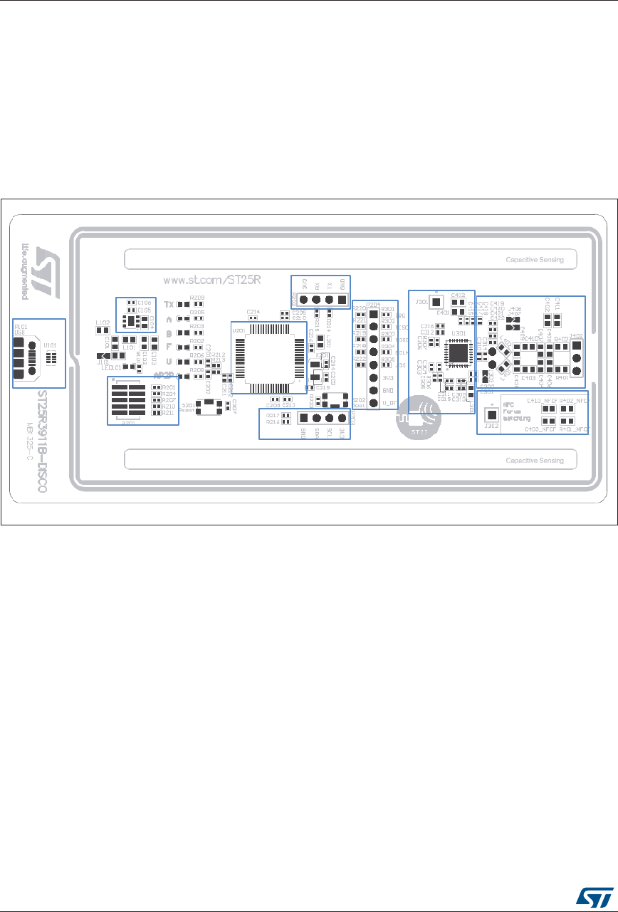
2.3.1 PCB overview
The PCB (see Figure 8) is organized in two halves
•Left side: the SPI header P204 and the digital / MCU sections
•Right side: the analog parts and the ST25R3911B.
The whole PCB is surrounded by a two turns NFC antenna.
Figure 8. PCB overview
The boot button can be found right above the I2C header. If this button is pressed during the
powering or the resetting of the board, the STM32L4 will enter the boot loader mode. The
reset button is positioned between the JTAG/SWD header and the I2C header.
2.3.2 PCB layers
The PCB layout is designed considering that the ST25R3911B is a high power RF
transmitter, hence the decoupling capacitors are located as close as possible to the positive
and negative power supply pins, for example VSP_RF and VSN_RF.
Since the chip is using a differential output driver stage, the antenna matching network is
treated as a differential network. The space between the components is kept as small as
possible and the whole network is routed in a completely symmetrical way.
Via stitching and via shielding is used to maintain a low impedance and prevent short return
current loops. The RF traces are protected by via stitching in combination with guard rings
to create a via wall. This keeps the PCB electromagnetically “quiet”.
A via shield is used to create a vertical copper barrier through the PCB. This helps to reduce
crosstalk and electromagnetic interference in any route carrying an RF signal. The RFI
traces and AAT lanes are routed as close as possible to each other.
670/
8$57
-7$*6:' ,&
63, 675%
1)&)RUXPPDWFKLQJ
86%
/'29 0DWFKLQJFRPSRQHQWV
069

DocID029132 Rev 2 15/25
UM2042 Hardware
24
Top layer
The top layer (Figure 9) contains most of the components and PCB traces. The unused
areas around the ICs are filled with GND planes, guarded using via stitching. Furthermore,
important analog traces are surrounded by GND vias.
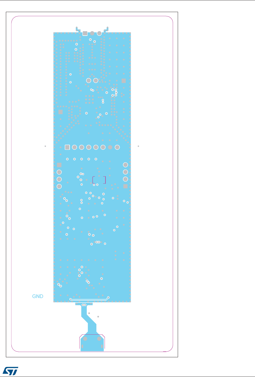
Mid layer 1
This layer (Figure 10) is a pure GND plane, providing a low ohmic DC path for the GND
connection.
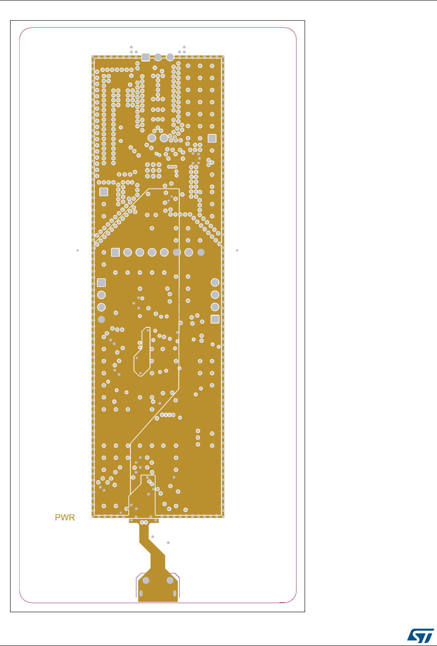
Mid layer 2
Mid layer 2 (Figure 11) is used for the power distribution. It contains the power planes for the
5 V supply of the ST25R3911B and the 3.3 V supply of the microcontroller.
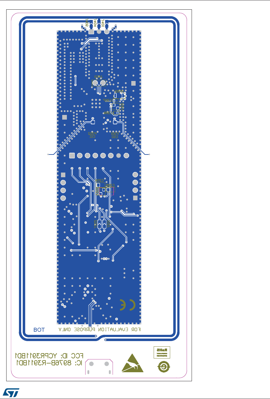
Bottom layer
The bottom layer (Figure 12) is mainly a GND plane, but some traces are routed through it.
Hardware UM2042
16/25 DocID029132 Rev 2
Figure 9. PCB layout, top layer
UM2042 Hardware
DocID029132 Rev 2 17/25
Figure 10. PCB layout, mid layer 1
Hardware UM2042
18/25 DocID029132 Rev 2
Figure 11. PCB layout, mid layer 2
UM2042 Hardware
DocID029132 Rev 2 19/25
Figure 12. PCB layout, bottom layer
Antenna matching UM2042
20/25 DocID029132 Rev 2
3 Antenna matching
The default matching network assembled enables VHBR operation up to 3.4 Mbps.
Components for an optional NFC Forum matching are placed on the board. Exchanging the
components as indicated in Table 1 will increase the Q factor of the antenna system. VHBR
communication at 3.4 Mbps and 1.7 Mbps bit rate will not be supported anymore, but the
read range for lower data rate applications will increase, up to 20%.
The matching impedance will remain the same when switching between the two matchings.
VHBR matching
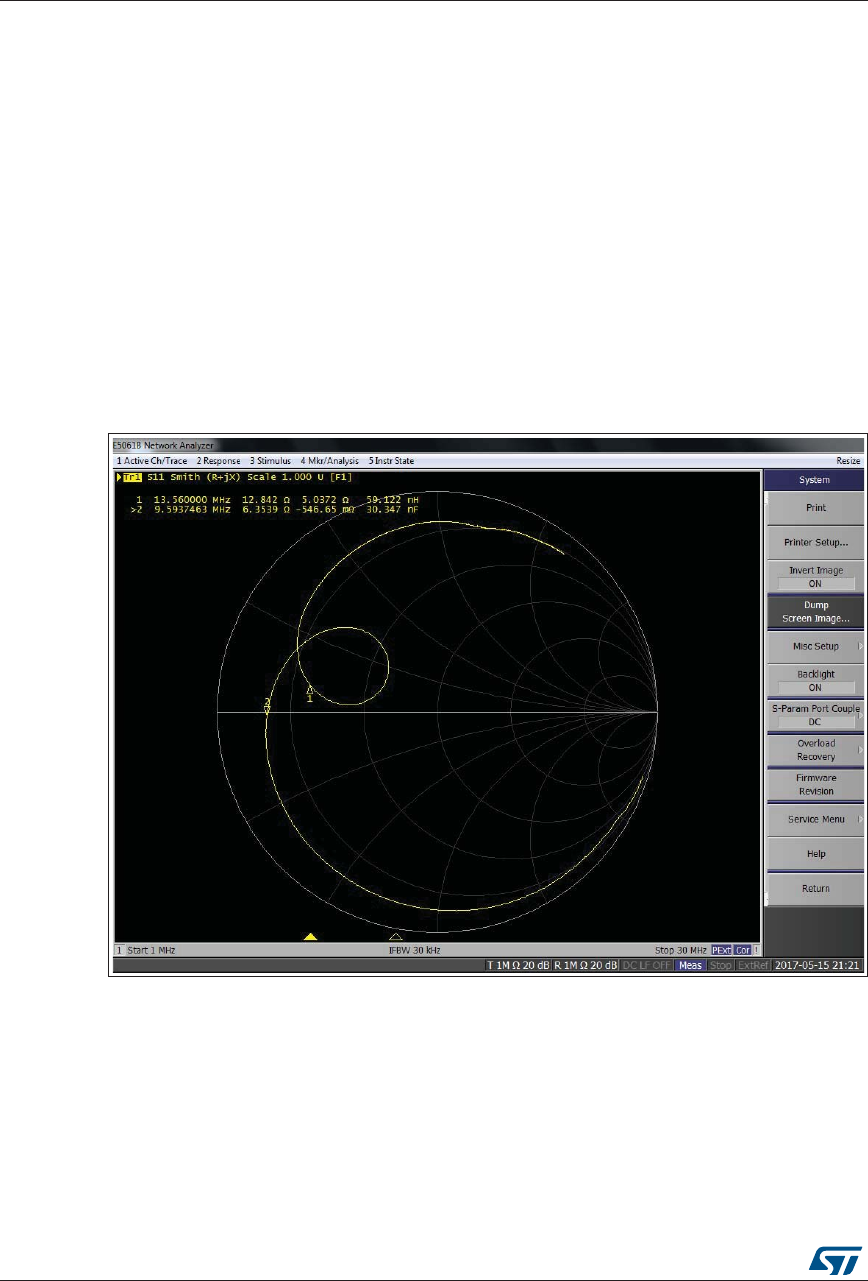
The VHBR matching is designed with a target Q-Factor of 8. The matching impedance is
around 12.8 + j5 . The HW based AAT algorithm will typically adjust to an AAT value of 8
(see Figure 13).
Figure 13. VHBR matching with an AAT setting of 8
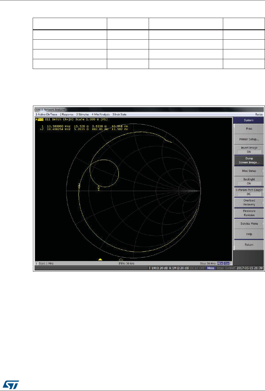
NFC Forum matching
The NFC Forum matching is designed with a target Q-Factor of 16.
To switch to the NFC Forum matching the user needs to change the components listed in
Table 1.
DocID029132 Rev 2 21/25
UM2042 Antenna matching
24
With the new assembled values, the matching impedance looks as in Figure 14, with a
value close to 11 + j6 .
Figure 14. NFC Forum matching with an AAT setting of 11
The HW based AAT algorithm will typically adjust to an AAT value of 11. Due to the higher
Q-Factor the voltage on the antenna is also increasing. To have the receiver in an optimum
signal level range, the capacitors C401 and C412 can be increased to 100 pF.
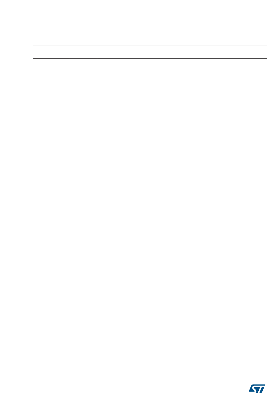
Table 1. NFC Forum matching alternatives
Default assembly Value NFC Forum replacement Value
C403 80 pF C403_NFCF 120 pF
C410 180 pF C410_NFCF 120 pF
R401 3R9 R401_NFCF 1R96
R402 3R9 R402_NFCF 1R96

Federal Communications Commission (FCC) and Industry Canada (IC) compliance statements
22/25 DocID029132 Rev 2
4 Federal Communications Commission (FCC)
and Industry Canada (IC) compliance statements
4.1 FCC Compliance Statement
4.1.1 Part 15.19
This device complies with Part 15 of the FCC Rules. Operation is subject to the following
two conditions: (1) this device may not cause harmful interference, and (2) this device must
accept any interference received, including interference that may cause undesired
operation.
4.1.2 Part 15.21
Any changes or modifications to this equipment not expressly approved by
STMicroelectronics may cause harmful interference and void the user’s authority to operate
this equipment.
4.1.3 Part 15.105
This equipment has been tested and found to comply with the limits for a Class B digital
device, pursuant to part 15 of the FCC Rules. These limits are designed to provide
reasonable protection against harmful interference in a residential installation. This
equipment generates, uses and can radiate radio frequency energy and, if not installed and
used in accordance with the instructions, may cause harmful interference to radio
communications. However, there is no guarantee that interference will not occur in a
particular installation. If this equipment does cause harmful interference to radio or
television reception, which can be determined by turning the equipment off and on, the user
is encouraged to try to correct the interference by one or more of the following measures:
•Reorient or relocate the receiving antenna.
•Increase the separation between the equipment and receiver.
•Connect the equipment into an outlet on a circuit different from that to which the
receiver is connected.
•Consult the dealer or an experienced radio/ TV technician for help.
4.1.4 FCC ID
FCC ID: YCPR3911BD1
4.2 Formal notices required by the Industry Canada (“IC”)
4.2.1 Compliance Statement
This device complies with Industry Canada license-exempt RSS standard(s). Operation is
subject to the following two conditions: (1) this device may not cause interference, and (2)
this device must accept any interference, including interference that may cause undesired
operation.

DocID029132 Rev 2 23/25
UM2042Federal Communications Commission (FCC) and Industry Canada (IC) compliance state-
24
4.2.2 Declaration de Conformité
Le présent appareil est conforme aux CNR d’Industrie Canada applicables aux appareils
radio exempts de licence. L’exploitation est autorisée aux deux conditions suivantes: (1)
l’appareil ne doit pas produire de brouillage, et (2) l’utilisateur de l’appareil doit accepter tout
brouillage radioélectrique subi, même si le brouillage est susceptible d’en compromettre le
fonctionnement.
4.2.3 IC ID
IC ID: 8976B-R3911BD1
Revision history UM2042
24/25 DocID029132 Rev 2
5 Revision history
Table 2. Document revision history
Date Revision Changes
23-Jun-2017 1 Initial release.
25-Jul-2017 2
Added Section 4.1.3: Part 15.105.
Updated Section 4.1.4: FCC ID and Section 4.2.3: IC ID.
Updated Figure 8: PCB overview, Figure 9: PCB layout, top layer and
Figure 12: PCB layout, bottom layer.

DocID029132 Rev 2 25/25
UM2042
25
IMPORTANT NOTICE – PLEASE READ CAREFULLY
STMicroelectronics NV and its subsidiaries (“ST”) reserve the right to make changes, corrections, enhancements, modifications, and
improvements to ST products and/or to this document at any time without notice. Purchasers should obtain the latest relevant information on
ST products before placing orders. ST products are sold pursuant to ST’s terms and conditions of sale in place at the time of order
acknowledgement.
Purchasers are solely responsible for the choice, selection, and use of ST products and ST assumes no liability for application assistance or
the design of Purchasers’ products.
No license, express or implied, to any intellectual property right is granted by ST herein.
Resale of ST products with provisions different from the information set forth herein shall void any warranty granted by ST for such product.
ST and the ST logo are trademarks of ST. All other product or service names are the property of their respective owners.
Information in this document supersedes and replaces information previously supplied in any prior versions of this document.
© 2017 STMicroelectronics – All rights reserved