Sagem Wireless 95MASV3C GSM 850/900/1800/1900 Module User Manual OEM Installation Instruction
Sagem Wireless GSM 850/900/1800/1900 Module OEM Installation Instruction
UserManual.wiki
>
Sagem Wireless
>
95MASV3C User Manual
OEM Installation Instruction
Navigation menu
Upload a User Manual
Namespaces
Wiki Guide
HTML
PDF
Info
Views
User Manual
Discussion / Help
Navigation
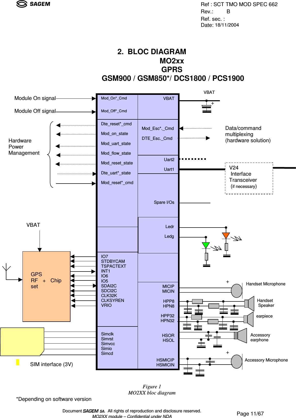
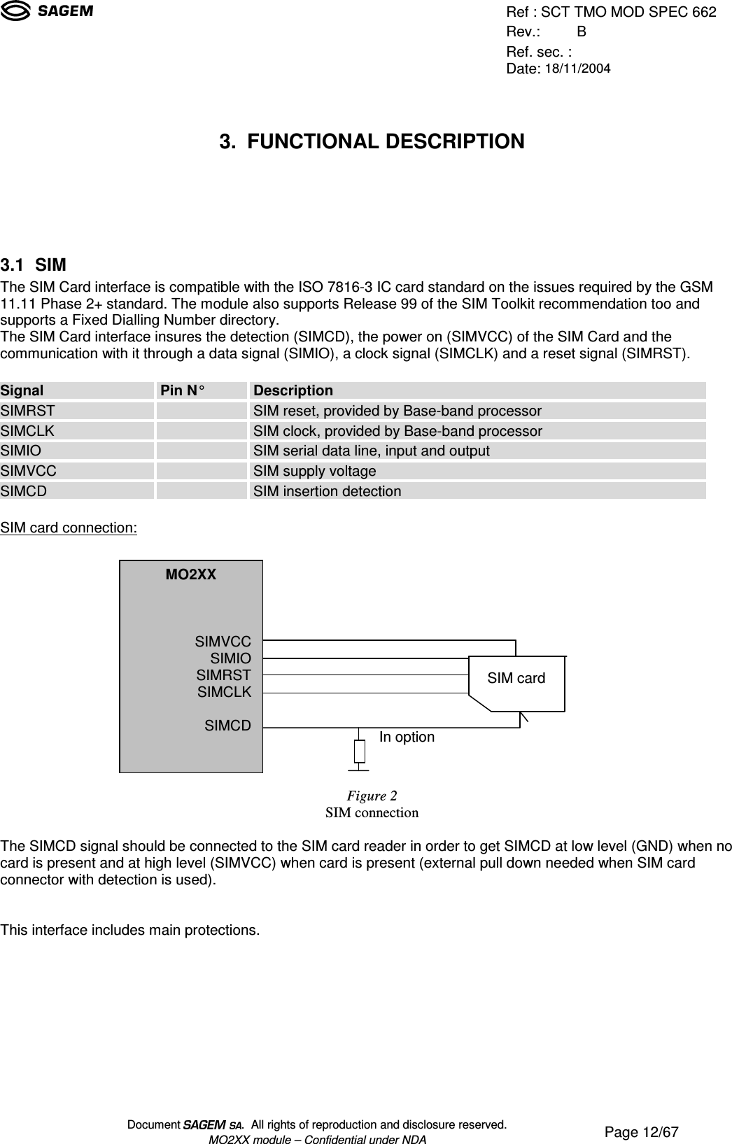
![Ref : SCT TMO MOD SPEC 662Rev.: BRef. sec. :Date: 18/11/2004Document . All rights of reproduction and disclosure reserved.MO2XX module – Confidential under NDA Page 6/671. OVERVIEW1.1 OBJECT OF THE DOCUMENTThis document gives an overview of the MO2XX module: a miniature, single-side board, quad-band GSM/GPRSmodule, ready for integration in wireless communicating device as a MODEM.The major functionalities offered by the MO2XX modules are:• The audio capabilities• The voice/data multiplexingThis document describes the main functionalities of this module: GPRS / GSM 900MHz / GSM 850MHz /DCS1800MHz / PCS 1900MHz, interface to the SIM card, the battery, and the audio (when available), as well as theelectrical interfaces, the mechanical specification (dimension, form…) and the electrical specification of the module.1.2 STANDARDS COMPLIANCE• [GSM 02.60]: "Digital cellular telecommunications system (Phase 2+); Stage 1 Service Description of theGeneral Packet Radio Service (GPRS)". Version 6.3.0.• [GSM 03.03]: "Digital cellular telecommunications system (Phase 2+); Numbering, addressing andidentification". Version 6.6.0.• [GSM 03.13]: "Digital cellular telecommunications system (Phase 2+); Discontinuous Reception (DRX) in theGSM system". Version 6.0.0.• [GSM 03.60]: "Digital cellular telecommunications system (Phase 2+); General Packet Radio Service (GPRS);Service description; Stage 2". Version 6.7.0.• [GSM 03.64]: "Digital cellular telecommunications system (Phase 2+); General Packet Radio Service(GPRS);Overall description of GPRS radio Interface; Stage 2". Version 6.4.0.• [GSM 04.02]: "Digital cellular telecommunications system (Phase 2+); GSM Public Land Mobile Network(PLMN) access reference configuration". Version 6.0.0.• [GSM 04.03]: "Digital cellular telecommunications system (Phase 2+); Mobile Station - Base Station System(MS - BSS) interface Channel structures and access capabilities". Version 6.0.0.• [GSM 04.04]: "Digital cellular telecommunications system (Phase 2+); Layer 1 General requirements". Version6.0.0.• [GSM 04.05]: "Digital cellular telecommunications system (Phase 2+); Data Link (DL) layer General aspects".Version 6.0.1.• [GSM 04.07]: "Digital cellular telecommunications system (Phase 2+); Mobile radio interface signalling layer 3General aspects". Version 6.5.1.• [GSM 04.08]: "Digital cellular telecommunications system (Phase 2+);Mobile radio interface layer 3specification". Version 6.11.0.• [GSM 04.60]: "Digital cellular telecommunications system (Phase 2+); General Packet Radio Service (GPRS);Radio Link Control/Medium Access Control (RLC/MAC) protocol". Version 6.9.0.• [GSM 04.64]: "Digital cellular telecommunications system (Phase 2+); General Packet Radio Service (GPRS);Logical Link Control (LLC)". Version 6.7.0.• [GSM 04.65]: "Digital cellular telecommunications system (Phase 2+); General Packet Radio Service (GPRS);Mobile Station (MS) - Serving GPRS Support Node (SGSN); Sub network Dependent Convergence Protocol(SNDCP)". Version 6.7.0.• [GSM 05.02]: "Digital cellular telecommunications system (Phase 2+); Multiplexing and multiple access on theradio path". Version 6.9.0.• [GSM 05.03]: "Digital cellular telecommunications system (Phase 2+); Channel coding". Version 6.2.1.](https://usermanual.wiki/Sagem-Wireless/95MASV3C/User-Guide-516547-Page-6.png)
![Ref : SCT TMO MOD SPEC 662Rev.: BRef. sec. :Date: 18/11/2004Document . All rights of reproduction and disclosure reserved.MO2XX module – Confidential under NDA Page 7/67• [GSM 05.08]: "Digital cellular telecommunications system (Phase 2+); Radio subsystem link control". Version6.8.0.• [GSM 05.10]: "Digital cellular telecommunications system (Phase 2+); Radio subsystem synchronization".Version 6.6.0.• AT command Set for Sagem Modules SCT TMO MOD SPEC 465 B• GCF-CC (V.3.16.0) and GT.01.• NAPRD.03 (V.2.10.1).1.3 COMPLIANCE WITH FCC GUIDELINESDevices incorporating MO2XX modules must be designed to maintain a minimum separation distance of 20 cmbetween the antenna and the end user to satisfy RF exposure requirements for mobile transmitting devices.1.4 TERMS AND ABBREVIATIONADC Analog to Digital ConverterADPCM Adaptive Delta Pulse Code ModulationAFC Automatic Frequency CorrectionASIC Application Specific Integrated CircuitBMP BitmapCODEC Coder-DecoderCTS Clear To SendDAC Digital to Analog ConverterDAI Digital Audio InterfaceDCS Digital Communications SystemDSP Data Signal ProcessorDSR Data Set ReadyDTR Data Terminal ReadyEGSM Enhanced GSMEMS Enhanced Messaging ServicesESD Electrostatic DischargeETS European Telecommunication StandardGSM Global System for Mobile communicationGPRS General Packet Radio ServicesIC Integrated CircuitIEEE Institute of Electrical and Electronics EngineersI/O Input / OutputIRDA Infra Red Device ApplicationISO International Standards OrganisationITU International Telecommunication UnionJPEG Joint Picture Expert GroupJTAG Joint Test Action GroupKbps Kbits per secondLCD Liquid Crystal DisplayLED Light Emitting DiodeLNA Low Noise AmplifierMbps Mbits per secondMIDI Musical Instrument Digital InterfaceMMI Man Machine interfacePA Power AmplifierPBCCH Packet Broadcast ChannelPCB Printed Circuit BoardPCS Personal Communication SystemPLL Phase Locked Loop](https://usermanual.wiki/Sagem-Wireless/95MASV3C/User-Guide-516547-Page-7.png)


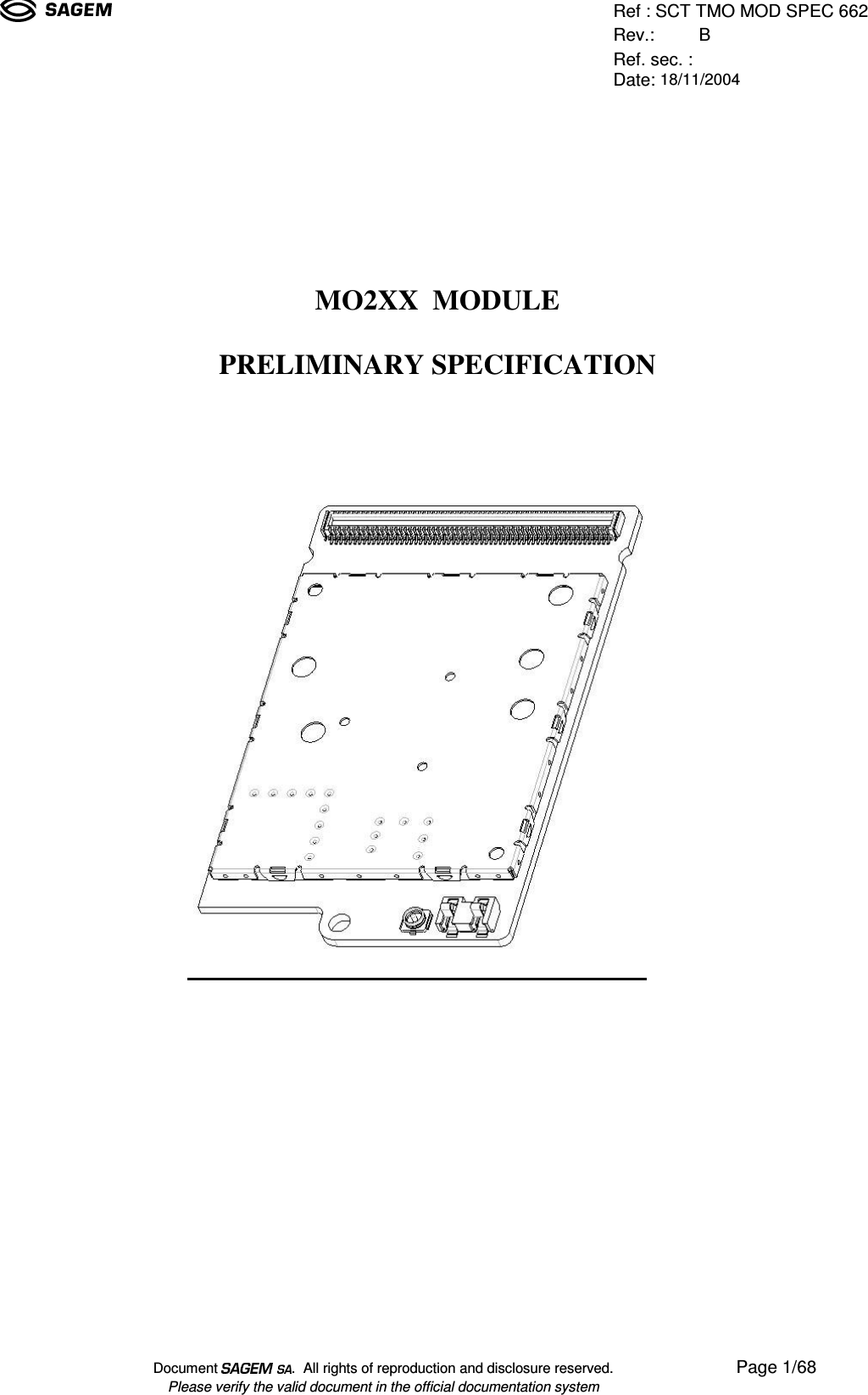
![Ref : SCT TMO MOD SPEC 662Rev.: BRef. sec. :Date: 18/11/2004Document . All rights of reproduction and disclosure reserved.MO2XX module – Confidential under NDA Page 28/675. DELTA LIST BETWEEN MO190 TO MO2XXThe MO2XX is inherited from the XS2xx. It aims to replace the MO190 module and to be compatible with it.Nevertheless, following discrepancies are noted:Compatibility issues MO190 MO2XXAudio signals BFTXP/N :1st gain : [-12, -6, 0, +6, +12, +18, +21] dB2nd gain : 4.6 or 28.2 dBHSMICIP/N : Only 25.6 dB(see § 6.11.2)Audio signals BFRXP/N : Nominal impedance : 150 ΩHSOL/R: Nominal impedance : 32 Ω (see§ 6.11.3)Audio signals MICP/NValue of the polarization : about 4VMICIP/N:Value of the polarization : 2.5V(see § 6.11.1)Audio signals HPP/N and LPHP HPP/N 8 and HPP/N 32 : maximum outputlevels are different between MO2XX andMO190Hardware incompatibility: 4 signals insteadof 3 signals(see § 6.12)Charger Voltage 0-16V Voltage 6-7VMOD_RESET*_CMD MOD_RESET*_CMD active low state Compliance with MO190 : to be verifiedDTE_RESET*_CMD VLmin = - 0.5VVLmax= + 0.8VVHmin= + 2.0VVhmax= + 3.2VElectrical incompatibility :VLmax= +0.59VVHmin= + 2.32VCLK13MCompatibilityMO190=>MO2XX:OKVLmax= +0.4VVHmin= + 2.4VElectrical incompatibility :VLmax= + 0.59VVHmin= + 2.32VCLK32KVLmax= +0.4VVHmin= + 1.6VElectrical incompatibility :VLmax= + 0.297VVHmin= + 1.32V](https://usermanual.wiki/Sagem-Wireless/95MASV3C/User-Guide-516547-Page-28.png)