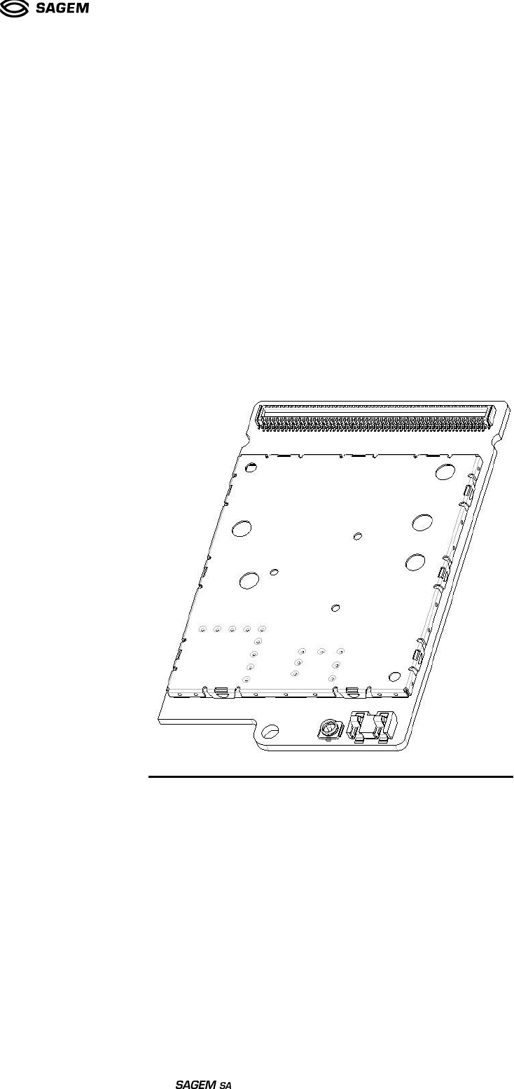
Sagem Wireless 95MASV3C GSM 850/900/1800/1900 Module User Manual OEM Installation Instruction
Sagem Wireless GSM 850/900/1800/1900 Module OEM Installation Instruction
OEM Installation Instruction
Ref : SCT TMO MOD SPEC 662
Rev.: B
Ref. sec. :
Date: 18/11/2004
Document . All rights of reproduction and disclosure reserved.
Please verify the valid document in the official documentation system
Page 1/68
MO2XX MODULE
PRELIMINARY SPECIFICATION
Ref : SCT TMO MOD SPEC 662
Rev.: B
Ref. sec. :
Date: 18/11/2004
Document . All rights of reproduction and disclosure reserved.
MO2XX module – Confidential under NDA Page 2/67
CHANGE HISTORY
Rev.
Date Author Reason for change
A08/09/2004 SAGEM S.A. First document
B18/11/2004 SAGEM S.A. Modifications of all §
TABLE OF CONTENTS
1. OVERVIEW
................................
................................
................................
....................
6
1.1 Object of the document
................................
................................
................................
....................
6
1.2 Standards compliance
................................
................................
................................
......................
6
1.3 compliance with fcc guidelines
................................
................................
................................
........
7
1.4 Terms and abbreviation
................................
................................
................................
....................
7
1.5 Conventions
................................
................................
................................
................................
.......
8
1.6 Product features
................................
................................
................................
................................
9
BLOC DIAGRAM
................................
................................
................................
...............
11
3. FUNCTIONAL DESCRIPTION
................................
................................
....................
12
3.1 SIM
................................
................................
................................
................................
....................
12
3.2 AUdio
................................
................................
................................
................................
................
13
3.3 Network LED
................................
................................
................................
................................
....
14
3.3.1 Network / Low BATTERY
................................
................................
................................
...........
14
3.3.2 Messages
................................
................................
................................
................................
...
14
3.3.3 Handfree call
................................
................................
................................
..............................
14
3.3.4 Summary chart
................................
................................
................................
...........................
15
3.4 Data
................................
................................
................................
................................
...................
15
3.4.1 Data services
................................
................................
................................
..............................
15
3.4.2 UART1: V24
................................
................................
................................
...............................
15
3.4.3 UART 2
................................
................................
................................
................................
.......
15
3.5 Antenna
................................
................................
................................
................................
............
16
3.6 DAI
................................
................................
................................
................................
.....................
16
3.7 Clocks
................................
................................
................................
................................
...............
16

Ref : SCT TMO MOD SPEC 662
Rev.: B
Ref. sec. :
Date: 18/11/2004
Document . All rights of reproduction and disclosure reserved.
MO2XX module – Confidential under NDA Page 3/67
3.8 Power management and charge
................................
................................
................................
....
16
3.8.1 Battery
................................
................................
................................
................................
........
16
3.8.2 VRIO
................................
................................
................................
................................
...........
17
3.8.3 Vbackup
................................
................................
................................
................................
.....
17
3.8.4 Charge
................................
................................
................................
................................
........
17
3.8.5 This interface includes main protections.AC/DC switching charger
................................
..........
17
3.8.5.1 Operating temperature
................................
................................
................................
............
17
3.8.5.2 Electrical ratings
................................
................................
................................
.....................
17
3.8.5.2.1 Primary input voltage
................................
................................
................................
........
17
3.8.5.2.2 Primary/secondary insulation
................................
................................
............................
17
3.8.5.2.3 Static output template
................................
................................
................................
.......
18
3.8.5.2.4 Dynamic output template
................................
................................
................................
..
18
3.8.5.2.5 Reverse current (main off)
................................
................................
................................
19
3.8.5.3 Thermal ratings
................................
................................
................................
.......................
19
3.8.6 Simple battery charger
................................
................................
................................
...............
19
3.9 Power management
................................
................................
................................
.........................
20
3.9.1 Interface identification and diagrams.
................................
................................
........................
20
3.9.2 Recommended strategy : software management
................................
................................
......
20
3.10 Data / Command multiplexing
................................
................................
................................
........
20
3.11 GLObal Positioning system (GPS) application
................................
................................
............
21
4. PINOUT
................................
................................
................................
.......................
22
5. DELTA LIST BETWEEN MO190 TO MO2XX
................................
.............................
28
6. ELECTRICAL SPECIFICATION
................................
................................
..................
30
6.1 VBAT
................................
................................
................................
................................
.................
30
6.2 VRIO
................................
................................
................................
................................
..................
31
6.3 DAI interface
................................
................................
................................
................................
.....
31
6.4 Network LED
................................
................................
................................
................................
....
31
6.5 SERIAL INTERFACE (µWIRE)
................................
................................
................................
.........
31
6.6 SIM
................................
................................
................................
................................
....................
31
6.7 V24 (UART 1)
................................
................................
................................
................................
....
32
6.8 UART2
................................
................................
................................
................................
...............
32
6.9 DATA / Command multiplexing
................................
................................
................................
......
32
6.10 Power management
................................
................................
................................
.........................
33
6.11 AudIO SIGNALS
................................
................................
................................
...............................
33
6.12 Charger
................................
................................
................................
................................
.............
34
6.13 Reset
................................
................................
................................
................................
.................
35
6.14 Spare IO
................................
................................
................................
................................
............
35

Ref : SCT TMO MOD SPEC 662
Rev.: B
Ref. sec. :
Date: 18/11/2004
Document . All rights of reproduction and disclosure reserved.
MO2XX module – Confidential under NDA Page 4/67
6.15 Clocks
................................
................................
................................
................................
...............
35
6.16 JTAG interface
................................
................................
................................
................................
.
35
7. ENVIRONMENTAL SPECIFICATION
................................
................................
.........
36
8. MECHANICAL SPECIFICATION
................................
................................
................
37
PHYSICAL DIMENSIONS
................................
................................
................................
............................
37
8.2 TERMINAL ASSIGNMENTS
................................
................................
................................
.............
40
8.2.1. 120 pins connector
................................
................................
................................
......................
40
8.2.1.1. MO2XX connector
................................
................................
................................
..................
40
8.2.1.2. Mother board connector
................................
................................
................................
..........
41
8.2.2. MO2XX Antenna connector
................................
................................
................................
.........
42
8.2.3. Battery connector
................................
................................
................................
........................
43
ANNEX 1 : IO DESCRIPTION
................................
................................
...........................
44
ANNEX 2 : HARDWARE POWER MANAGEMENT
................................
..........................
48
Different strategies
................................
................................
................................
................................
....
48
1. Interface specification.
................................
................................
................................
.......................
48
1.1 Management by DCE alone.
................................
................................
................................
...
48
1.3.1. Signals.
................................
................................
................................
...............................
49
1.3.2. Signals and states.
................................
................................
................................
..............
50
Logical and electrical levels:
................................
................................
................................
..............
51
1.3.3.1. Transition tables.
................................
................................
................................
..............
51
1.3.3.2. Command signals.
................................
................................
................................
...........
51
1.3.3.3. Transition from OFF to ON Active.
................................
................................
..................
52
1.3.3.4. Transition from ON Active to ON Sleep.
................................
................................
.........
52
1.3.3.4.1. Initiated by DTE.
................................
................................
................................
........
53
1.3.3.4.2. Initiated by DCE.
................................
................................
................................
.......
54
1.3.3.4.3. Transitory states.
................................
................................
................................
.......
55
1.3.3.5. Transition from ON Sleep to ON Active.
................................
................................
.........
56
1.3.3.5.1. Initiated by the DCE.
................................
................................
................................
.
57
1.3.3.5.2. Initiated by DTE.
................................
................................
................................
........
57
1.3.3.6. Transition from ON Sleep to OFF.
................................
................................
..................
58
1.3.3.7. Transition from ON Active to OFF.
................................
................................
..................
59
1.3.3.8. Reset
................................
................................
................................
...............................
61
1.3.3.8.1. Initiated by the DCE.
................................
................................
................................
.
62
1.3.3.8.2. Initiated by the DTE.
................................
................................
................................
..
63
1.3.3.9. Timeout.
................................
................................
................................
...........................
63
ANNEX 3 : DATA/COMMAND HARDWARE MULTIPLEXING
................................
.........
64
1. Hardware multiplexing
................................
................................
................................
.......................
64
1.1. External interfaces
................................
................................
................................
......................
64
1.2. Capability requirements
................................
................................
................................
.............
64
1.2.1. Logical and electrical levels
................................
................................
................................
64
1.2.2. Hardware protocol
................................
................................
................................
...............
64
1.2.3. State diagram
................................
................................
................................
......................
65
1.2.4. Transition (1): Command -> Data
................................
................................
.......................
65
1.2.5. Transition (2): Data -> Suspended Data
................................
................................
.............
65
1.2.6. Transition (3): Suspended Data -> Data Mode
................................
................................
...
66

Ref : SCT TMO MOD SPEC 662
Rev.: B
Ref. sec. :
Date: 18/11/2004
Document . All rights of reproduction and disclosure reserved.
MO2XX module – Confidential under NDA Page 5/67
1.2.7. Transition (4): Suspended Data -> Command Mode
................................
..........................
66
1.2.8. Timeout case
................................
................................
................................
.......................
67

Ref : SCT TMO MOD SPEC 662
Rev.: B
Ref. sec. :
Date: 18/11/2004
Document . All rights of reproduction and disclosure reserved.
MO2XX module – Confidential under NDA Page 6/67
1. OVERVIEW
1.1 OBJECT OF THE DOCUMENT
This document gives an overview of the MO2XX module: a miniature, single-side board, quad-band GSM/GPRS
module, ready for integration in wireless communicating device as a MODEM.
The major functionalities offered by the MO2XX modules are:
• The audio capabilities
• The voice/data multiplexing
This document describes the main functionalities of this module: GPRS / GSM 900MHz / GSM 850MHz /DCS
1800MHz / PCS 1900MHz, interface to the SIM card, the battery, and the audio (when available), as well as the
electrical interfaces, the mechanical specification (dimension, form…) and the electrical specification of the module.
1.2 STANDARDS COMPLIANCE
• [GSM 02.60]: "Digital cellular telecommunications system (Phase 2+); Stage 1 Service Description of the
General Packet Radio Service (GPRS)". Version 6.3.0.
• [GSM 03.03]: "Digital cellular telecommunications system (Phase 2+); Numbering, addressing and
identification". Version 6.6.0.
• [GSM 03.13]: "Digital cellular telecommunications system (Phase 2+); Discontinuous Reception (DRX) in the
GSM system". Version 6.0.0.
• [GSM 03.60]: "Digital cellular telecommunications system (Phase 2+); General Packet Radio Service (GPRS);
Service description; Stage 2". Version 6.7.0.
• [GSM 03.64]: "Digital cellular telecommunications system (Phase 2+); General Packet Radio Service
(GPRS);Overall description of GPRS radio Interface; Stage 2". Version 6.4.0.
• [GSM 04.02]: "Digital cellular telecommunications system (Phase 2+); GSM Public Land Mobile Network
(PLMN) access reference configuration". Version 6.0.0.
• [GSM 04.03]: "Digital cellular telecommunications system (Phase 2+); Mobile Station - Base Station System
(MS - BSS) interface Channel structures and access capabilities". Version 6.0.0.
• [GSM 04.04]: "Digital cellular telecommunications system (Phase 2+); Layer 1 General requirements". Version
6.0.0.
• [GSM 04.05]: "Digital cellular telecommunications system (Phase 2+); Data Link (DL) layer General aspects".
Version 6.0.1.
• [GSM 04.07]: "Digital cellular telecommunications system (Phase 2+); Mobile radio interface signalling layer 3
General aspects". Version 6.5.1.
• [GSM 04.08]: "Digital cellular telecommunications system (Phase 2+);Mobile radio interface layer 3
specification". Version 6.11.0.
• [GSM 04.60]: "Digital cellular telecommunications system (Phase 2+); General Packet Radio Service (GPRS);
Radio Link Control/Medium Access Control (RLC/MAC) protocol". Version 6.9.0.
• [GSM 04.64]: "Digital cellular telecommunications system (Phase 2+); General Packet Radio Service (GPRS);
Logical Link Control (LLC)". Version 6.7.0.
• [GSM 04.65]: "Digital cellular telecommunications system (Phase 2+); General Packet Radio Service (GPRS);
Mobile Station (MS) - Serving GPRS Support Node (SGSN); Sub network Dependent Convergence Protocol
(SNDCP)". Version 6.7.0.
• [GSM 05.02]: "Digital cellular telecommunications system (Phase 2+); Multiplexing and multiple access on the
radio path". Version 6.9.0.
• [GSM 05.03]: "Digital cellular telecommunications system (Phase 2+); Channel coding". Version 6.2.1.

Ref : SCT TMO MOD SPEC 662
Rev.: B
Ref. sec. :
Date: 18/11/2004
Document . All rights of reproduction and disclosure reserved.
MO2XX module – Confidential under NDA Page 7/67
• [GSM 05.08]: "Digital cellular telecommunications system (Phase 2+); Radio subsystem link control". Version
6.8.0.
• [GSM 05.10]: "Digital cellular telecommunications system (Phase 2+); Radio subsystem synchronization".
Version 6.6.0.
• AT command Set for Sagem Modules SCT TMO MOD SPEC 465 B
• GCF-CC (V.3.16.0) and GT.01.
• NAPRD.03 (V.2.10.1).
1.3 COMPLIANCE WITH FCC GUIDELINES
Devices incorporating MO2XX modules must be designed to maintain a minimum separation distance of 20 cm
between the antenna and the end user to satisfy RF exposure requirements for mobile transmitting devices.
1.4 TERMS AND ABBREVIATION
ADC Analog to Digital Converter
ADPCM Adaptive Delta Pulse Code Modulation
AFC Automatic Frequency Correction
ASIC Application Specific Integrated Circuit
BMP Bitmap
CODEC Coder-Decoder
CTS Clear To Send
DAC Digital to Analog Converter
DAI Digital Audio Interface
DCS Digital Communications System
DSP Data Signal Processor
DSR Data Set Ready
DTR Data Terminal Ready
EGSM Enhanced GSM
EMS Enhanced Messaging Services
ESD Electrostatic Discharge
ETS European Telecommunication Standard
GSM Global System for Mobile communication
GPRS General Packet Radio Services
IC Integrated Circuit
IEEE Institute of Electrical and Electronics Engineers
I/O Input / Output
IRDA Infra Red Device Application
ISO International Standards Organisation
ITU International Telecommunication Union
JPEG Joint Picture Expert Group
JTAG Joint Test Action Group
Kbps Kbits per second
LCD Liquid Crystal Display
LED Light Emitting Diode
LNA Low Noise Amplifier
Mbps Mbits per second
MIDI Musical Instrument Digital Interface
MMI Man Machine interface
PA Power Amplifier
PBCCH Packet Broadcast Channel
PCB Printed Circuit Board
PCS Personal Communication System
PLL Phase Locked Loop

Ref : SCT TMO MOD SPEC 662
Rev.: B
Ref. sec. :
Date: 18/11/2004
Document . All rights of reproduction and disclosure reserved.
MO2XX module – Confidential under NDA Page 8/67
PNG Portable Network Graphics
RAM Random Access Memory
RF Radio Frequency
RI Ring Indication
RMS Root Mean Square
RTS Ready To Send
RX Reception
SIM Subscriber Identification Module
SMS Short Message Service
SRAM Static Random Access Memory
TBC To Be Confirmed
TBD To Be Defined
TX Transmission
UART Universal Asynchronous Receiver and Transmitter
USB Universal Serial Bus
USSD Unstructured Supplementary Service Data
VCO Voltage Controlled Oscillator
WAP Wireless Application Protocol
WBMP Wide Bitmap
1.5 CONVENTIONS
Throughout this document, DTE (Data Terminal equipment) indicates the equipment which masters and controls
the module device MO2XX by simply sending AT commands via its serial interface.
DCE (Data Communication Equipment) indicates the module device MO2XX.
Ref : SCT TMO MOD SPEC 662
Rev.: B
Ref. sec. :
Date: 18/11/2004
Document . All rights of reproduction and disclosure reserved.
MO2XX module – Confidential under NDA Page 9/67
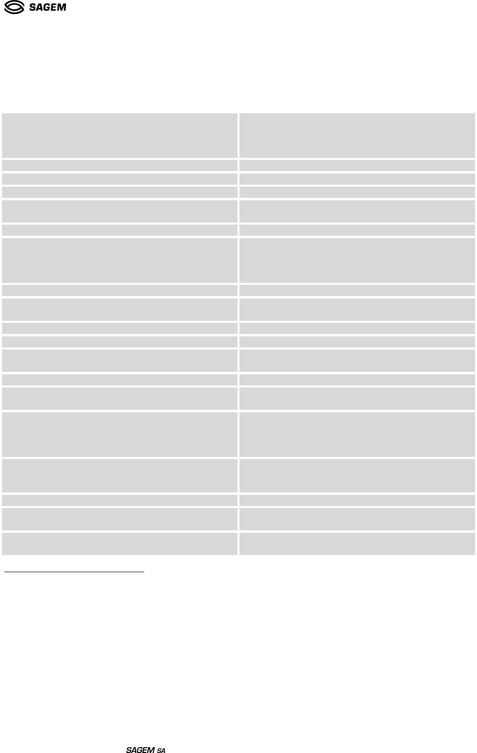
1.6 PRODUCT FEATURES
Temperature range
Normal range: -10°C to +55°C (fully compliant)
Extended range: -20°C to –10°C and +55°C to +70°C
(functional without any risk for the network)
Storage: -40°C to °85°C
Weight (in g) 10g
ESD ESD protection < 1.5 kV
Physical dimensions 34x54.4x3 mm (typical)
Connection 120 pins connector + 1 antenna connection + 1
battery connection
Power supply 3.45V to 4.5V range, 3.8V nominal.
Power consumption
1
Off mode: 120 uA (typ)
Stand-by mode: < 2.5 mA (typ)
Communication mode: 280 mA (typ at Pmax), 2.2 A
peak during TX slot
Power supply connector Dedicated connector
Battery charge management and interface Battery charge management is included. The charger
interface is provided on 120 pins connector.
Antenna No antenna included in the module.
Frequency bands GSM850 + EGSM900 + DCS1800 + PCS1900
Voice codecs Half Rate, Full Rate, Enhanced Full Rate,
Adaptive Multi Rate
GSM class Small MS
Transmit power Class 4 (2W) for GSM850 / EGSM900
Class 1 (1W) for DCS1800 / PCS1900
Supported SIM card
3V SIM cards.
To prevent SIM card’s damages, the power supply of
the module has to be turned off before any
manipulation of the SIM card.
SIM slot Not included on the module. Signals for the
management of the SIM card are provided on 120
pins connector
Network LED LEDR and LEDG management.
Audio up-link 2 differential inputs are provided for microphone
(accessories and handset).
Audio down-link 2 differential outputs are provided for non stereo
earphone and 1 differential output for accessories.
1
The power consumption is highly dependent on customer’s software and global environment of GSM Module
(MMI, Accessories,…).
Ref : SCT TMO MOD SPEC 662
Rev.: B
Ref. sec. :
Date: 18/11/2004
Document . All rights of reproduction and disclosure reserved.
MO2XX module – Confidential under NDA Page 10/67
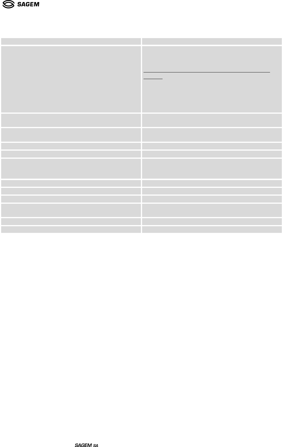
D.A.I GSM DAI test mode interface
UART1 interface with flow control
Up to 115.2 Kbaud with auto bauding.
Full flow control signals (+2.8V) are provided on ball-
out.
If a full compliant RS232 (+/-5V) serial interface is
needed:
The drivers (like MAX3232, ST3237CD, …) are not
included in the module and have to be added on the
main PCB.
A proven schematic to build the RS232 interface is
provided in application note.
Data/command multiplexing Hardware management of data/command
multiplexing on the serial link UART1
Power management Hardware management of sleeping and waking in
module /DTE architecture
UART2 interface Up to 115.2 Kbaud.
Data services GPRS, CSD, Fax
Supplementary services (supported via AT
commands, refer to SCT TMO MOD SPEC 465 B)
Caller Line Identification, Call Waiting, Call Hold, Call
Forwarding, Multiparty, Call Barring, Advice of
Charge, USSD, CPHS
Reset pin Available (reset of all the system including backup)
Power on pin Available
General purpose I/Os pin 3 x I/O, 1 interrupt, 1 ADC available
GPRS SMG 31bis, Multi slot class 10, class B terminal,
PBCCH support
GSM/DCS certification GCF-CC V.3.16.0 and GT.01
PCS certification NAPRD.03 (V.2.10.1)
Ref : SCT TMO MOD SPEC 662
Rev.: B
Ref. sec. :
Date: 18/11/2004
Document . All rights of reproduction and disclosure reserved.
MO2XX module – Confidential under NDA Page 11/67
2. BLOC DIAGRAM
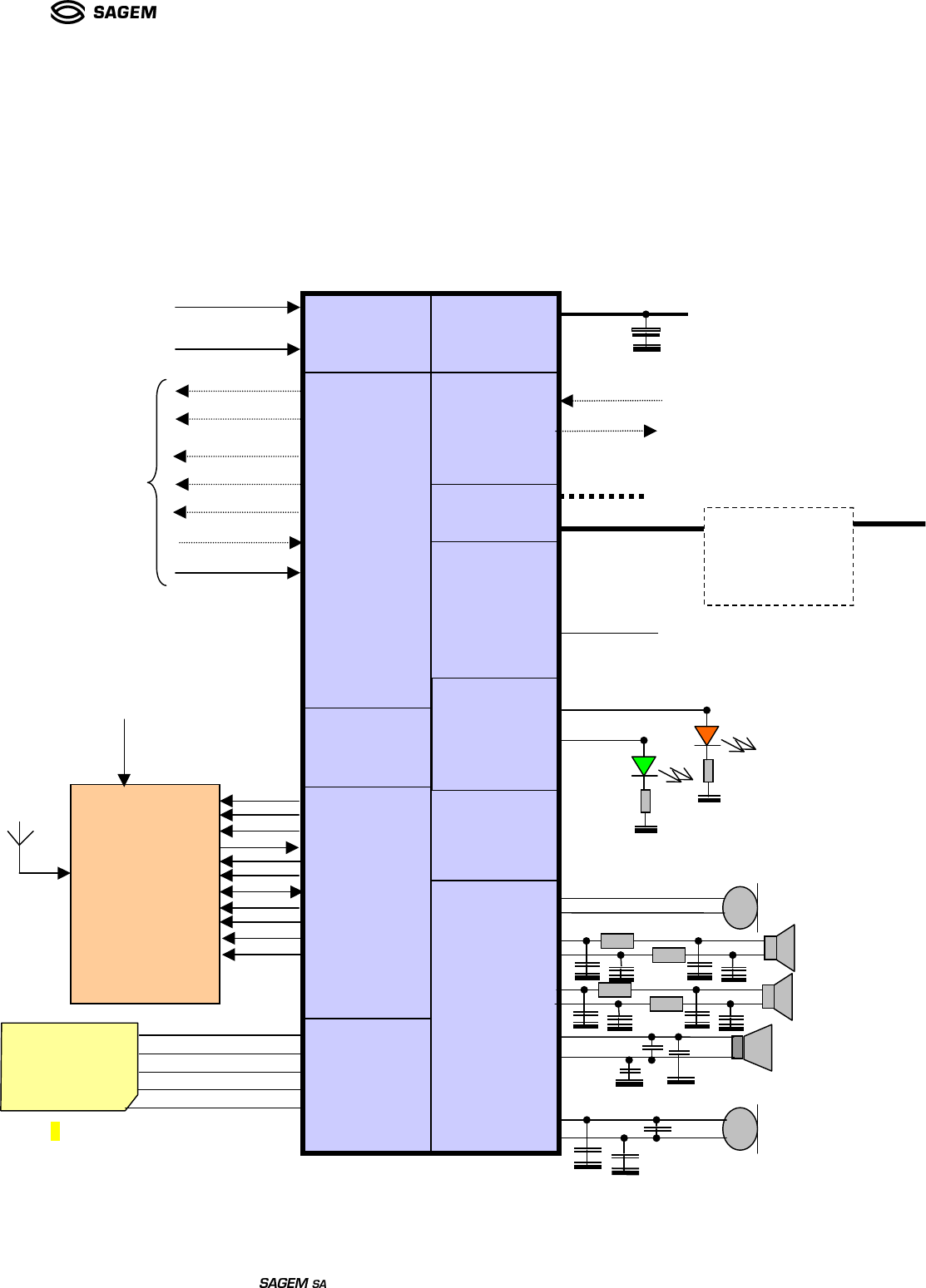
Figure 1
MO2XX bloc diagram
*Depending on software version
MO2xx
GPRS
GSM900 / GSM850*/ DCS1800 / PCS1900
Hardware
Power
Management
+
SIM interface (3V)
Mod_On*_Cmd
Mod_Off*_Cmd
Dte_reset*_cmd
Mod_on_state
Mod_uart_state
Mod_flow_state
Mod_reset_state
Dte_uart*_state
Mod_reset*_cmd
IO7
STDBYCAM
TSPACTEXT
INT1
IO6
IO5
SDAI2C
SDCI2C
CLK32K
CLKSYREN
VRIO
Simclk
Simrst
Simvcc
Simio
Simcd
MICIP
MICIN
HPP8
HPN8
HPP32
HPN32
HSOR
HSOL
HSMICIP
HSMICIN
Ledr
Ledg
Spare I/Os
Uart2
Uart1
Mod_Esc*._Cmd
DTE_Esc._Cmd
+
+
VBAT
Handset Microphone
Handset
Speaker
Module On signal
VBAT
Module Off signal
V24
Interface
Transceiver
(if necessary)
Accessory Microphone
Accessory
earphone
earpiece
Data/command
multiplexing
(hardware solution)
GPS
RF + Chip
set
VBAT
Ref : SCT TMO MOD SPEC 662
Rev.: B
Ref. sec. :
Date: 18/11/2004
Document . All rights of reproduction and disclosure reserved.
MO2XX module – Confidential under NDA Page 12/67
3. FUNCTIONAL DESCRIPTION
3.1 SIM
The SIM Card interface is compatible with the ISO 7816-3 IC card standard on the issues required by the GSM
11.11 Phase 2+ standard. The module also supports Release 99 of the SIM Toolkit recommendation too and
supports a Fixed Dialling Number directory.
The SIM Card interface insures the detection (SIMCD), the power on (SIMVCC) of the SIM Card and the
communication with it through a data signal (SIMIO), a clock signal (SIMCLK) and a reset signal (SIMRST).
Signal Pin N° Description
SIMRST SIM reset, provided by Base-band processor
SIMCLK SIM clock, provided by Base-band processor
SIMIO SIM serial data line, input and output
SIMVCC SIM supply voltage
SIMCD SIM insertion detection
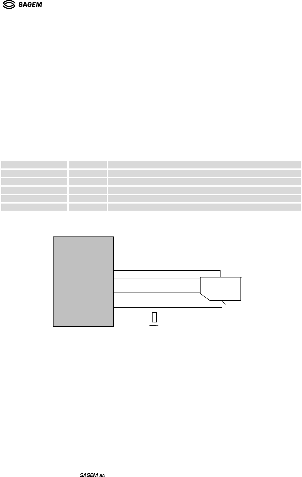
SIM card connection:
Figure 2
SIM connection
The SIMCD signal should be connected to the SIM card reader in order to get SIMCD at low level (GND) when no
card is present and at high level (SIMVCC) when card is present (external pull down needed when SIM card
connector with detection is used).
This interface includes main protections.
MO2XX
SIMVCC
SIMIO
SIMRST
SIMCLK
SIMCD
SIM card
In option
Ref : SCT TMO MOD SPEC 662
Rev.: B
Ref. sec. :
Date: 18/11/2004
Document . All rights of reproduction and disclosure reserved.
MO2XX module – Confidential under NDA Page 13/67
3.2 AUDIO
The module supports the following voice codecs:
• Half-Rate
• Full-Rate
• Enhanced Full Rate
• Adaptive Multi Rate
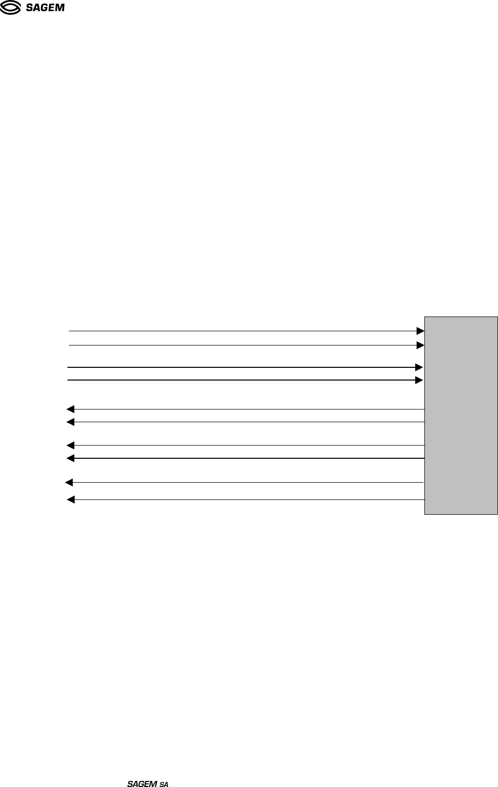
It manages an external handset microphone (MICIP/MICIN) and an external handset earphone (32 Ohms
HPP32/HPN32 and 6 to 8 Ohms HPP8/HPN8) in differential mode.
The bias voltage of the microphone is provided directly on MICIP/MICIN pins.
There are two options for the earphone:
- Two earphones, one 32 Ohms as earpiece and one 6 Ohms minimum as Ring/melody and as hands-free
loudspeaker if it is far from the microphone.
- one 32 Ohms earphone as earpiece.
The module can also manage accessories (earphone and microphone) through dedicated lines
(HSMICIP/HSMICIN for microphone and HSOL/HSOR for stereo earphone). The typical impedance for the
earphone is 150 Ohms.
Figure 3
Audio
This interface includes main protections.
To ensure proper operation of such sensitive signals, there have to be isolated from the other by ground on mother
board layout.
NB: To avoid destruction of module components, the HP inductance has to be 47nH +/- 5% @ 200MHz
Base-band
Ampli+Filter
MICIP
MICIN
HSMICIP
P
HSMICIN
HPP32
HPN32
HSOR
HSOL
HPP8
HPN8
Ref : SCT TMO MOD SPEC 662
Rev.: B
Ref. sec. :
Date: 18/11/2004
Document . All rights of reproduction and disclosure reserved.
MO2XX module – Confidential under NDA Page 14/67
3.3 NETWORK LED
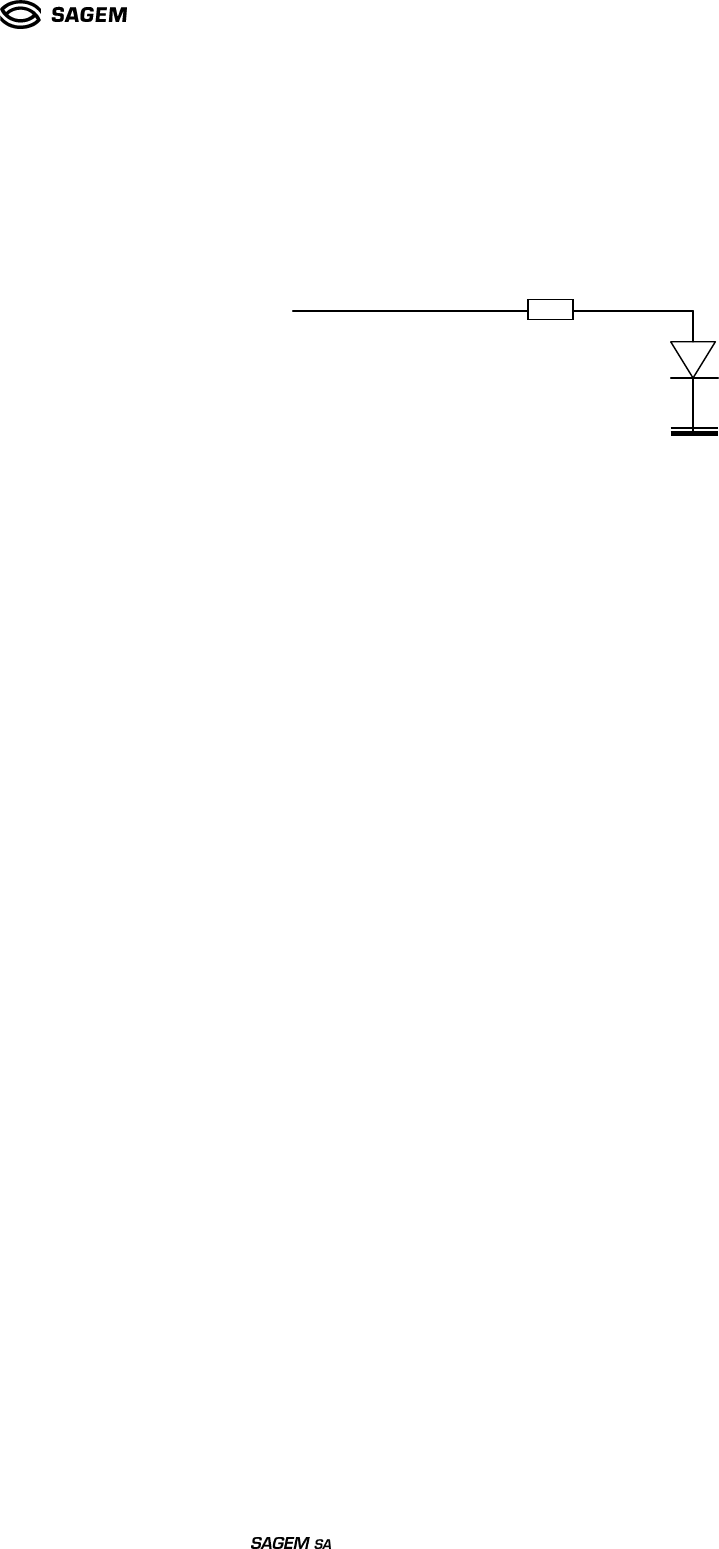
Two external pins of the module are dedicated to network and alarm LEDs:
- LEDR
- LEDG
Figure 4
Network LED connection
3.3.1 Network / Low BATTERY
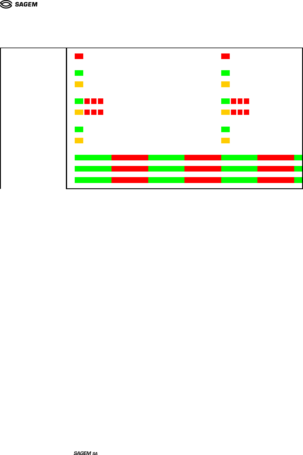
The network/battery indication consist in by a 30ms flash with period of 2 s.
The flash can take 3 colors:
• green when network attached and battery ok.
• orange (green + red) network attached and battery low.
• red no network and battery low.
The battery threshold is 3650 mV.
3.3.2 Messages
The message received indication takes place after the network/battery indication, it consists in 3 successive
20ms red flashes. It indicates the presence of a new SMS or voice mailbox.
3.3.3 Handfree call
During a handfree call (with at+vip=1 during a call), the led becomes alternately red and green with a period
of 1 s. Handfree led mode has priority over other modes (Network,Messages…)
LEDR or
LEDG
Ref : SCT TMO MOD SPEC 662
Rev.: B
Ref. sec. :
Date: 18/11/2004
Document . All rights of reproduction and disclosure reserved.
MO2XX module – Confidential under NDA Page 15/67
3.3.4 Summary chart
Battery low :
Network :
+ battery low :
Message received :
(SMS, voice / not read)
+ battery low :
Communication :
+ battery low :
Communication (handsfree) :
+ battery low :
(no effect)
+message:
(no effect)
3.4 DATA
3.4.1 Data services
The module supports the following services:
• GPRS
• CSD: transparent and non-transparent up to 9600 BPS
• Fax: class 1 group 3
3.4.2 UART1: V24
A V24 interface is provided on external pins of the module with the following signals:
- RTS/CTS
- RX/TX
- DSR
- DTR
- DCD
- RI
It supports speeds up to 115.2 KBPS and may be used in auto bauding mode.
Two supplementary signals (MOD_ESCAPE*_CMD, DTE_ESCAPE_CMD) are provided to toggle from data
mode to command mode on this serial link.
3.4.3 UART 2
It is strongly recommended to leave this interface externally accessible for Debug.
There is no flow control on this interface.
Ref : SCT TMO MOD SPEC 662
Rev.: B
Ref. sec. :
Date: 18/11/2004
Document . All rights of reproduction and disclosure reserved.
MO2XX module – Confidential under NDA Page 16/67
3.5 ANTENNA
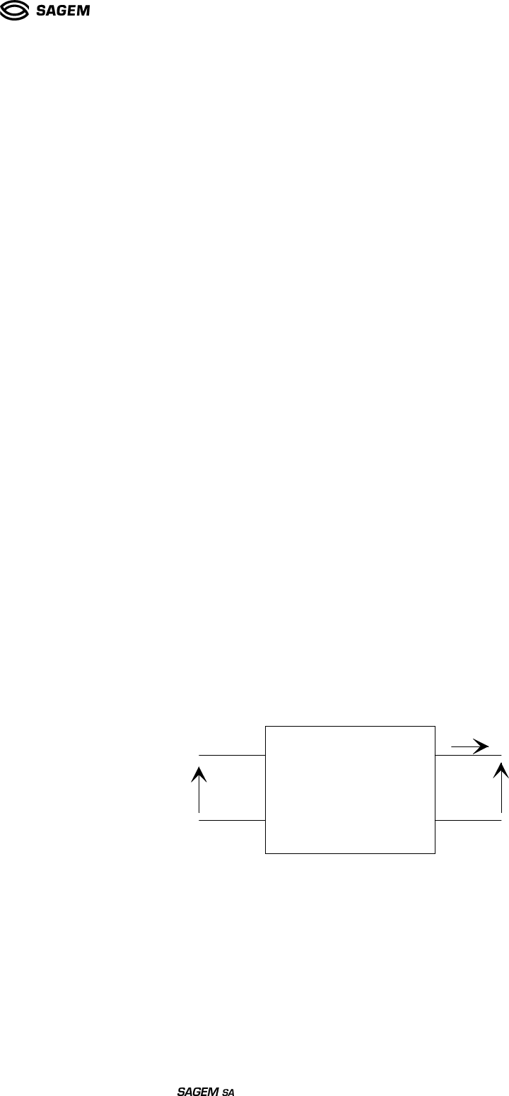
Two accesses for the antenna connection are provided.
- one by mean of a 50ohms connector
- one by mean of a simple copper area
Figure 5
Antenna area on the MO2XX
See into Application Note for more details.
3.6 DAI
A DAI interface is provided on the module for type approval tests.
3.7 CLOCKS
A 32KHz frequency clock and a 13MHz frequency digital clock are provided on external pins of the module.
To ensure proper operation of such sensitive signals, they have to be isolated from the other by ground on mother
board layout.
3.8 POWER MANAGEMENT AND CHARGE
3.8.1 Battery
The power supply signal VBAT is 3.45V to 4.5V range and 3.8V nominal.
Only Li-Ion battery are supported.
It has to be more than 3.2V, even during transients in order to avoid unwanted resets. The power supply dropout
has to be limited to 450mV, when the current consumption goes from minimum to maximum (0.1 to 2A). The noise
level of the power supply has to be limited to 50mV RMS in the 100KHz – 1MHz frequency range
SAGEM advises to use Sanyo or LG battery. If battery is used, SAGEM agreement is needed (slight qualification
tests).
Only battery with 200mOhms maximum internal resistor are managed by the module.
Antenna ground
copper area
Antenna copper pad
50 Ohms connector
Ref : SCT TMO MOD SPEC 662
Rev.: B
Ref. sec. :
Date: 18/11/2004
Document . All rights of reproduction and disclosure reserved.
MO2XX module – Confidential under NDA Page 17/67
3.8.2 VRIO
+2.8V output is available on external pin of the module and could supply +2.8V external components (current
capability 10mA in active mode).
This interface includes main protections.
3.8.3 Vbackup
External Backup could be supply through the VBACKUP input (from 2.2V to 3.2V). A internal mechanism is present
to charge the backup battery.
If No external Backup is supplied, VBACKUP input has to be connected to VBAT signal.
3.8.4 Charge
This interface manages the charge of the battery for regulated charger, when a charger is connected, even in the
following conditions: deeply discharged battery, short-circuited battery and unconnected battery (600mA with
regulated charger).
The interface manages the charge of some regulated chargers, that have to be qualified by SAGEM (see listing in
application note).
WARNING :
The charger interface must be connected with wide tracks (1 mm width / 17.5um height tracks on the MO2XX ) to
allow 600 mA maximum current from the charger.
When using MO2XX as slave MODEM of a Host system sharing the same power supply (example : PDA), it is
strongly recommended to manage the charging function on Host side: so, in such a case, do not use the charge
function of the module.
3.8.5 This interface includes main protections.AC/DC switching charger
3.8.5.1 Operating temperature
0°C to +55°C.
3.8.5.2 Electrical ratings
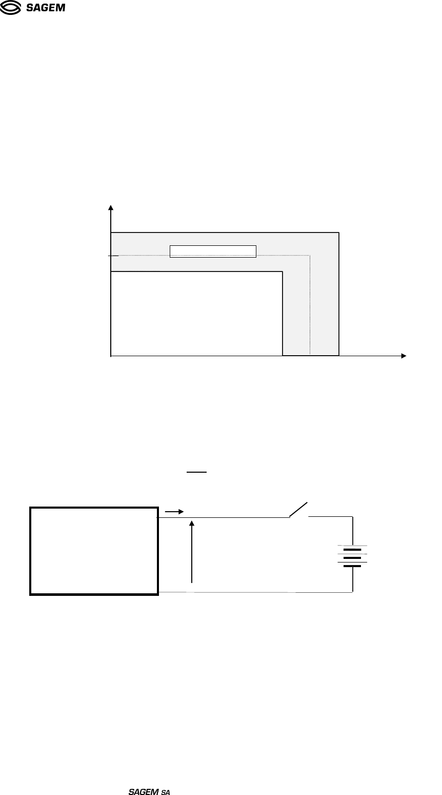
Vs
Is
Vp
Battery charger
Figure 6
Charging.
Class II equipment (EN 60950 § 1-2-4-2)
3.8.5.2.1 Primary input voltage
98V < Vp < 254V ; F = 50/60Hz.
3.8.5.2.2 Primary/secondary insulation
Security transformer class E (EN 60950 § 5-1)
Ref : SCT TMO MOD SPEC 662
Rev.: B
Ref. sec. :
Date: 18/11/2004
Document . All rights of reproduction and disclosure reserved.
MO2XX module – Confidential under NDA Page 18/67
Electric strength : reinforced insulation (EN 60950 § 5-3-2)
3.8.5.2.3 Static output template
Figure 7
Charging valid area.
3.8.5.2.4 Dynamic output template
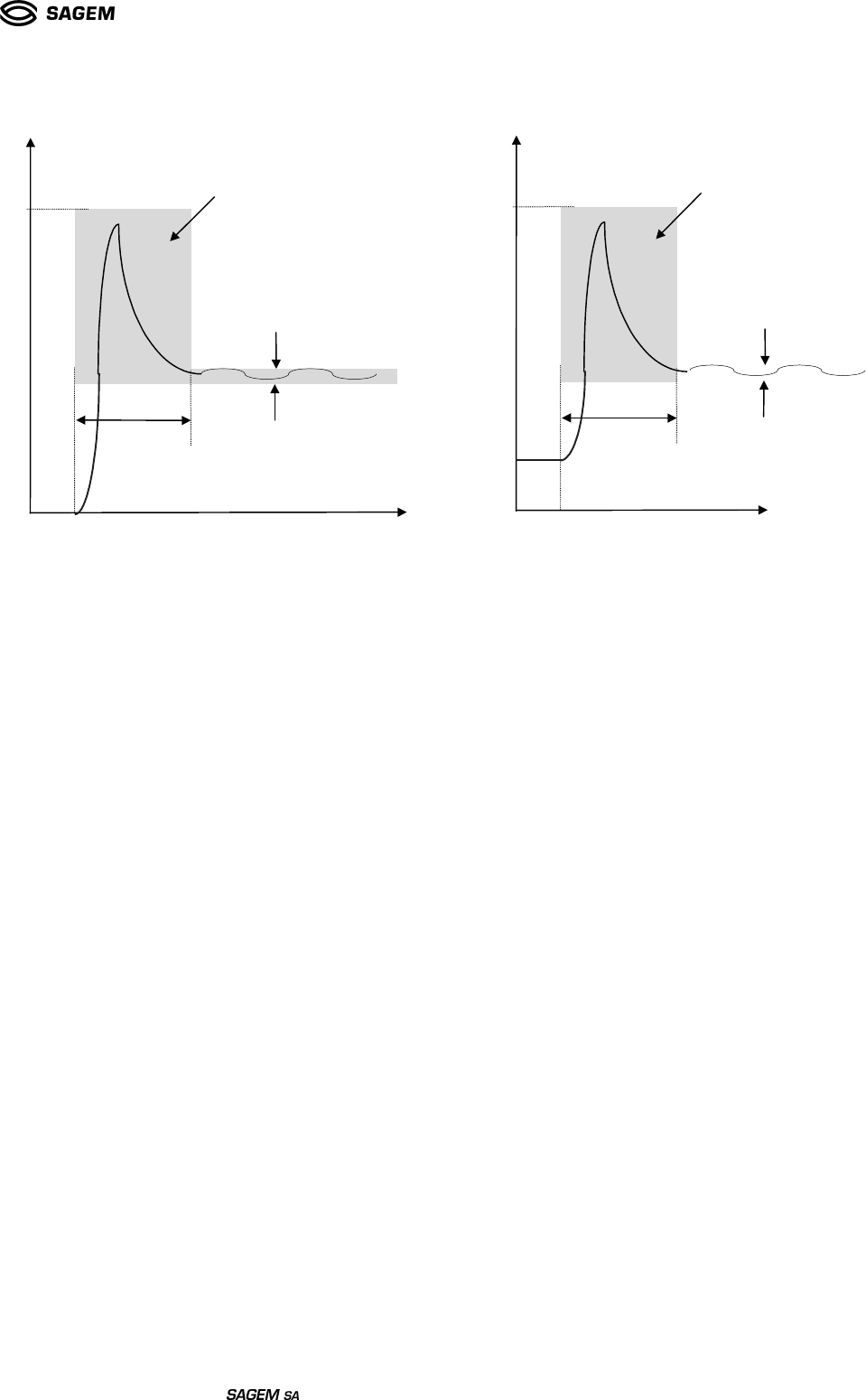
An external device is controlling the battery charge by means of a switch S1, which can be switched on and off.
Following templates shows the output current and voltage during transients, this feature is very important to enable
the charging control by controlling S1 (PWM).
Warning: These are the most important characteristics for a charger (it concerns the safety of the MO2XX
module). A charger has to be (at least) fully compliant with the current and voltage transients.
Figure 8
Charge principle.
550 mA
450 mA
Is
Vs
6V
7V
0
500 mA
VALID AREA
BATTERY CHARGER
0V <Vbat< 4.5V
Vs
Is
S1
Ref : SCT TMO MOD SPEC 662
Rev.: B
Ref. sec. :
Date: 18/11/2004
Document . All rights of reproduction and disclosure reserved.
MO2XX module – Confidential under NDA Page 19/67
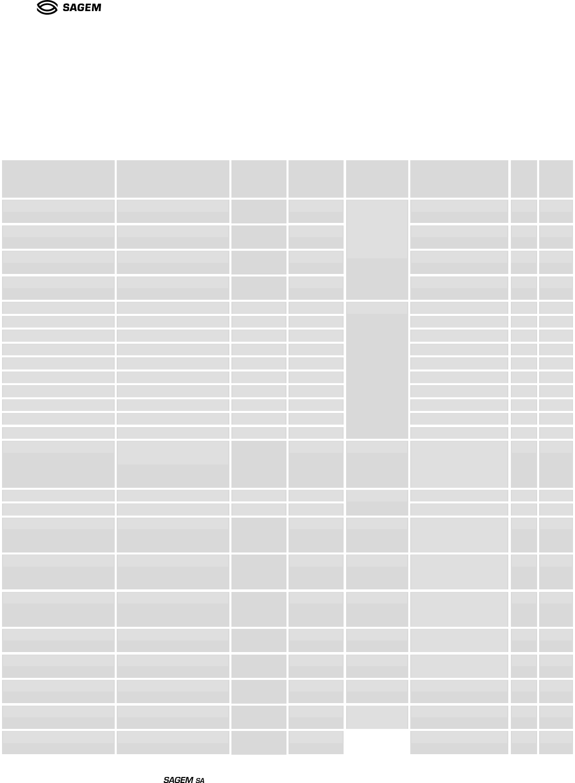
Figure 9
Transients in charge: Current transients & Voltage transients.
3.8.5.2.5 Reverse current (main off)
Main off or unplug, the current flowing from the battery to the charger have to stay smaller than « Ir » in order to
prevent discharge !
Ir < 100µA for Vbat ≤≤ 5V
3.8.5.3 Thermal ratings
The heating of the enclosure will comply with EN 60950 § 5-1
Tab. 16 - part 2.
3.8.6 Simple battery charger
Ask SAGEM to check compatibility for this kind of charger.
Is (dynamic)
Time
5A Max
5ms Max
S1 is
switched on
VALID AREA
Ripple : +/- 50mA
Vs (dynamic)
Time
20V Max
0.2ms Max
S1 is
switched off
VALID AREA
Ripple : +/- 200mV

Ref : SCT TMO MOD SPEC 662
Rev.: B
Ref. sec. :
Date: 18/11/2004
Document . All rights of reproduction and disclosure reserved.
MO2XX module – Confidential under NDA Page 20/67
3.9 POWER MANAGEMENT
3.9.1 Interface identification and diagrams.
On an external point of view (i.e. as seen by a DTE), the MO2XX has 4 different states:
• OFF:
In this state, none of the MO2XX functionality are running (the serial link is switched off)
• ON Sleep:
In this state, the MO2XX is asleep and the external serial link is switched off. Any interrupt will wake the
module up as well as the external serial link. An interrupt can be generated by reception of a character
but it is lost.
NB: in this state, the module is attached to the GSM network.
• ON Active:
In this state, the MO2XX is switched on and the serial link is activated. The MO2XX is able to receive
correctly the data sent by the DTE.
NB: in this state, the module is attached to the GSM network.
• Reset:
This state indicates that the MO2XX is in its setup procedure and implies that the serial link is
deactivated.
3.9.2 Recommended strategy : software management
A software management of the power consumption can be handled via the GSM 07.10 protocol.
Other strategies are possible and they are developed in the Annex 2.
3.10 DATA / COMMAND MULTIPLEXING
The serial link between the DCE and a DTE (PDA, phone,…) is used to send two different kinds of data
flow: AT commands and PPP data packets. these two flows cannot be mixed together (not enough
bandwidth). So, this serial link can be used in two different exclusive modes:
- Command Mode: The serial link is reserved for the AT Commands flow
- Data Mode: The serial link is reserved for the data flow
But, during a data connection, the modem or the DTE may need to send some AT Commands to notify the
other side of a major event. As there is just one serial link to send these two kinds of data, it is necessary
to have a special procedure to switch from one kind to the other.
• The first solution provided by the GSM standard is to use +++ and ATO. This solution very simple to
implement, has the main drawback to allow only the DTE to control the switch between the 2 modes and it is
usually only used to hang up a data call.

Ref : SCT TMO MOD SPEC 662
Rev.: B
Ref. sec. :
Date: 18/11/2004
Document . All rights of reproduction and disclosure reserved.
MO2XX module – Confidential under NDA Page 21/67
• The second solution consists to implement the GSM 07.10 standard, this solution is available (customer has to
develop its own driver for the host). SAGEM recommends to use this solution.
• A third method, developed by SAGEM S.A. and explained in details hereafter in the annex 3, consists to create
a third mode for the serial link and handle it through hardware signals. This mode is called “Suspended Data
Mode” and is temporarily used to send AT Commands. All data must to be stored during a Suspended data
mode switch. In the case of no-response from DTE, We need to implement a cyclic mechanism to change the
hardware signals states.
3.11 GLOBAL POSITIONING SYSTEM (GPS) APPLICATION
A GPS application can be implemented in the product. See application note for more detail.
Ref : SCT TMO MOD SPEC 662
Rev.: B
Ref. sec. :
Date: 18/11/2004
Document . All rights of reproduction and disclosure reserved.
MO2XX module – Confidential under NDA Page 22/67
4. PINOUT
MO2XX MO190 Required
operation for
electrical
compatibility
IO type Function MO2XX
Description
Pin N°
XS2xx
Pin N°
MO190
Or
MO2xx
DAIRST DAIRST Not
required Input DAI reset M4 116
DAIOUT DAIOUT Not
required Output DAI output data M3 115
DAIIN DAIIN Not
required Input DAI input data M2
117
DAICLK DAICLK Not
required Input
DAI
interface
(for
certification
tests only)
DAI clock L2 118
USL1 Input - T5
USL2 Output - S4
USL3 Output - S5
USL4 Output - S6
USL5 Output R3
USL6 (IO3) Output - R4
USL7 Input -
O17
USL8 Input -
P17
USL9 Input -
P16
USL10 Input
Useless
-
Q17
MOD_ESCAPE*_CMD MOD_ESCAPE*_CMD Not
required Input Command mode
request signal (from
DTE to MO2XX)
interrupt
L14
18
USL11 Input -
M15
USL12 Output
Useless
-
M14
DTE_ESCAPE_CMD DTE_ESCAPE_CMD Not
required Output Command mode
request signal (from
MO2XX to DTE)
L13
23
MOD_RESET_STATE MOD_RESET_STATE Not
required Output Signal showing a
RESET occurrence
of the module
M13
24
MOD_UART_STATE MOD_UART_STATE Not
required Output Signal giving the
state of the serial
link in the module
M12
25
MOD_FLOW_STATE MOD_FLOW_STATE Not
required Output Signal giving the
state of the module
M16
26
MOD_ON_STATE MOD_ON_STATE Not
required Output Signal giving the
state of the module
L15
27
MOD_ON*_CMD MOD_ON*_CMD Not
required Input ON signal Module ON signal
B10
113
SIMVCC SIMVCC Not
required Output SIM power supply T7 6
SIMRST SIMRST Not
required Output
SIM
interface
SIM reset T8 5
Ref : SCT TMO MOD SPEC 662
Rev.: B
Ref. sec. :
Date: 18/11/2004
Document . All rights of reproduction and disclosure reserved.
MO2XX module – Confidential under NDA Page 23/67
SIMCLK SIMCLK Not
required Output SIM clock T9 4
SIMIO SIMIO Not
required In/output SIM data
T10
7
SIMCD SIMCD Not
required Input SIM insertion
detection
B12
114
HSMICIP BFTXP
Audio level
Input Differential input
from microphone
O15
52
HSMICIN BFTXN
Audio level
Input
To external
microphone
(accessory)
Differential input
from microphone
P14
53
HSOL BFRXN
Audio level
Output
O14
50
HSOR BFRXP
Audio level
Output
To external
stereo HP
(accessory)
Differential output to
earphone
O13
49
MICIP MICP
Audio level
Input Differential input to
handset microphone
R15
63
MICIN MICN
Audio level
Input
Microphone
interface
Differential input to
handset microphone
Q15
62
HPP32
New signal
Output Differential output to
32ohms handset
earphone
N11
46
HPN32 LPHPN
New signal
Output
Earphone
interface
Differential output to
32ohms handset
earphone
O11
47
HPP8 HPP
Audio level
Output Differential output to
8ohms handset
earphone
O10
56
HPN8 HPN
Audio level
Output Differential output to
8ohms handset
earphone
N10
57
USL13 Output Useless -
M17
RI RI Not
required Output Ring Indicator N5 109
DSR DSR Not
required Output Data Send Ready E3 94
DCD DCD Not
required Output Data Carrier Detect E2 110
DTR DTR Not
required Input Data Terminal
Ready D3 95
CTS CTS Not
required Output Clear To Send C5 82
RTS RTS Not
required Input Request To Send D4 83
TXD1 TXD1 Not
required Output UART transmit 1 B5 101
RXD1 RXD1 Not
required Input
V24
interface
with flow
control
UART receive 1 B7 105
TXD2 TXD2 Not
required Output UART transmit 2 B8 103
RXD2 RXD2 Not
required Input
UART2
interface
UART receive 2 B9 104
INT1 SPRINT (CINT) Not
required Input Spare interrupt Q3 111
SCLI2C (ex USL15) SCLI2C Not
required Output
Useless
-
C11
14
Ref : SCT TMO MOD SPEC 662
Rev.: B
Ref. sec. :
Date: 18/11/2004
Document . All rights of reproduction and disclosure reserved.
MO2XX module – Confidential under NDA Page 24/67
SDAI2C (ex USL16) SDAI2C Not
required In/out -
B11
93
DTE_UART*_STATE DTE_UART*_STATE Not
required Input Signal giving the
state of the DTE H6 92
CHARGEUR CHARGEUR Only 6.5V
charger Input Battery
charging
interface
Charge O3,
O4,
O5
69, 70
MOD_OFF*_CMD MOD_OFF*_CMD Not
required Input Module OFF signal
interrupt N6 76
USL17 In/output - K5
USL18 In/output - K4
USL19 In/output - K3
USL20 In/output - K2
USL21 In/output - J2
USL22 In/output - J3
USL23 In/output - J4
USL24 In/output - I4
USL25 In/output - I3
USL26 In/output - I2
USL27 In/output - H2
USL28 In/output - H3
USL29 In/output - H4
USL30 In/output - G4
USL31 In/output - G3
USL32 In/output - G2
USL33 Output - I5
USL34 Output - F5
USL35 Output
Useless
- F6
USL36 Output - F4
USL37 Output - F3
USL38 Output - F2
USL39 In/output - I13
USL40 In/output -
N18
USL41 In/output -
L16
USL42 In/output - I12
USL43 In/output -
G17
USL44 In/output -
K15
USL45 In/output -
H15
USL46 In/output - I15
USL47 Output - I14
USL48 Output -
H13
USL49 Output -
G12
USL50 Output - I16
USL51 Output
Useless
-
J16
DTE_RESET*_CMD
(ex RESETLCD*) DTE_RESET*_CMD
(ex CMDSW2) Electrical
level Output DTE reset signal N2 106
USL52 In/output
N16
USL53 In/output
-
N17
USL54 Input
Useless
-
T15
USL55 Output
C17
USL56 In/output
Useless
- Q8
Ref : SCT TMO MOD SPEC 662
Rev.: B
Ref. sec. :
Date: 18/11/2004
Document . All rights of reproduction and disclosure reserved.
MO2XX module – Confidential under NDA Page 25/67
USL57 In/output - Q9
USL58 Input -
O16
USL59 Output - M8
USL60 Output -
K12
USL61 In/output -
D10
USL62 In/output - C4
USL63 In/output - C8
USL64 In/output -
E11
USL65 In/output -
EC6
USL66 In/output -
F10
USL67 In/output - C9
USL68 In/output - D5
USL69 Output -L3
USL70 Output - M5
USL71 Input -
C10
USL72 Output -L5
USL73 Output -L4
USL74 Output -
C15
USL75 Output -
H12
USL76 Output - I9
USL77 Output - E4
USL78 Output - D9
USL79 Output - D6
USL80 Input - D8
USL81 Output - E8
USL82 In/output -
D12
USL83 In/output -
B15
USL84 In/output -
B16
USL85 In/output -
B17
USL86 Output -
D11
USL87 Output -
B13
USL88 Input -
C12
CLK13M CLK13M Not
required
Compatibi
lity
MO190=>
MO2XX
Output 13MHz digital clock
output
L12
16
CLK32K CLK32K Electrical
level Output
Useless
32KHz digital clock
output R7 9
ADC2 ADC1 Hardware
interfacing
Input - Q5 11
USL90 Input -
C13
USL91 Output -
D13
USL92 In/output -
E12
USL93 In/output - E9
IO5 ITFLAP
New signal
In/output N4 80
IO6 A_0<>
New signal
In/output N3 65
IO7 SPRIO
CMDSW 1 Electrical
level In/output
Useless
J5 107
LEDR LEDR Electrical
level output LED P2 91

Ref : SCT TMO MOD SPEC 662
Rev.: B
Ref. sec. :
Date: 18/11/2004
Document . All rights of reproduction and disclosure reserved.
MO2XX module – Confidential under NDA Page 26/67
LEDG LEDG Electrical
level output Q2 90
TSPACTEXT A_4<>
New signal
output
Radio signal
C17
67
STBYCAM A_5 <>
New signal
output standby M5 66
CSMIW2* CSMIW2 Electrical
level Output Serial
interface for
LED chipset
Chip select for
backlight component
R3 97
CSMIW1* CSMIW1 Electrical
level Output LCD Driver chip
select of the serial
link
S6 98
DIMIW DIMIW Not
required Input LCD driver input
data of serial link T5 86
CKMIW CKMIW Not
required Output LCD driver clock of
serial link S5 85
DOMIW DOMIW Not
required output
Serial
interface to
connect
LCD or chip
melody (1
chip select)
LCD driver output
data of serial link S4 84
MOD_RESET*_CMD TESTRST* Electrical
level Input
Reset system signal
P4 81
VBAT VBAT Electrical
level Input Power
supply +3.8V battery power
supply (nominal) F19,
F20,
F21,
F22,
F23,
G19
,G2
0,H1
9,H2
0
Bat.
conn.
1,2
VRIO VRIO Electrical
level Output +2.8V output power
supply Q4 2
VBACKUP VBACKUP Not
required Input - P5 12
GND GND Not
required Ground Ground GND 8, 10,
15,
17,
48,
51,
54,
58,
60,
61, 64
Bat.
Conn
3,4
ANTENNE OUT_ANT Not
required Output/inp
ut Antenna
input/output
Antenna connection
(50 ohms) I23 Ant.
Conn.
TCK TCLK Not
required Input JTAG
T11
Test
point
TMS TMS Not
required Input JTAG
T14
Test
point
TDIDIGIT TDI Not
required Input JTAG
C14
Test
point
TDODIGIT TDODIGIT Not
required Output JTAG
D17
Test
point
TDIANALOG TDIANALOG Not
required Input
JTAG
interface
(SAGEM
use only)
JTAG R9 Test
point
Ref : SCT TMO MOD SPEC 662
Rev.: B
Ref. sec. :
Date: 18/11/2004
Document . All rights of reproduction and disclosure reserved.
MO2XX module – Confidential under NDA Page 27/67
TDOANALOG TDOANALOG Not
required Output JTAG P7 Test
point
BSCAN* NBSCAN Not
required Input JTAG
D16
Test
point
EMU0* NEMU0 Not
required Output For debug
C18
Test
point
EMU1* NEMU1 Not
required Output For debug
B18
Test
point
NC NC Not connected Q21
,R21
,R20
,S20
, L1,
P3,
Q6,
R5,
O2
* active on low electrical state
WARNING:
The USL signals are useless in MO2XX versions, these signals are not connected to the pins of the 120 pts
connector.
The USL signals shall not be connected to any other signal neither to ground on the mother board.

Ref : SCT TMO MOD SPEC 662
Rev.: B
Ref. sec. :
Date: 18/11/2004
Document . All rights of reproduction and disclosure reserved.
MO2XX module – Confidential under NDA Page 28/67
5. DELTA LIST BETWEEN MO190 TO MO2XX
The MO2XX is inherited from the XS2xx. It aims to replace the MO190 module and to be compatible with it.
Nevertheless, following discrepancies are noted:
Compatibility issues MO190 MO2XX
Audio signals BFTXP/N :
1st gain : [-12, -6, 0, +6, +12, +18, +21] dB
2nd gain : 4.6 or 28.2 dB
HSMICIP/N : Only 25.6 dB
(see § 6.11.2)
Audio signals BFRXP/N : Nominal impedance : 150 Ω
HSOL/R: Nominal impedance : 32 Ω (see
§ 6.11.3)
Audio signals MICP/N
Value of the polarization : about 4V
MICIP/N:
Value of the polarization : 2.5V
(see § 6.11.1)
Audio signals HPP/N and LPHP HPP/N 8 and HPP/N 32 : maximum output
levels are different between MO2XX and
MO190
Hardware incompatibility: 4 signals instead
of 3 signals
(see § 6.12)
Charger Voltage 0-16V Voltage 6-7V
MOD_RESET*_CMD MOD_RESET*_CMD active low state Compliance with MO190 : to be verified
DTE_RESET*_CMD VLmin = - 0.5V
VLmax= + 0.8V
VHmin= + 2.0V
Vhmax= + 3.2V
Electrical incompatibility :
VLmax= +0.59V
VHmin= + 2.32V
CLK13M
Compatibility
MO190=>MO2XX:OK
VLmax= +0.4V
VHmin= + 2.4V
Electrical incompatibility :
VLmax= + 0.59V
VHmin= + 2.32V
CLK32K
VLmax= +0.4V
VHmin= + 1.6V
Electrical incompatibility :
VLmax= + 0.297V
VHmin= + 1.32V
Ref : SCT TMO MOD SPEC 662
Rev.: B
Ref. sec. :
Date: 18/11/2004
Document . All rights of reproduction and disclosure reserved.
MO2XX module – Confidential under NDA Page 29/67
LEDG Imax = 4 mA Electrical level : to be verified
LEDR Imax = 4 mA Electrical level : to be verified
VBAT Vmax = 5V Electrical limitation : Vmax = 4.5V
V56 available Hardware incompatibility : not available
VRIO Current capability sleep mode = 1 mA Electrical limitation :
Current capability sleep mode = 0.5 mA
ADC2 ADC1 Hardware interfacing :
5.7Kohms on MO190
12pF on MO2XX
IO5 New signal
IO6 New signal
IO7 SPRIO =CMDSW1, Imax = 4 mA Electrical limitation : IO7, Imax = 2 mA
TSPACTEXT New signal
STBYCAM New signal
ALIMLCD available Not available
SPI bus Available Not available
Parallel bus (16bit) Available Not available
Ref : SCT TMO MOD SPEC 662
Rev.: B
Ref. sec. :
Date: 18/11/2004
Document . All rights of reproduction and disclosure reserved.
MO2XX module – Confidential under NDA Page 30/67
6. ELECTRICAL SPECIFICATION
VOH High level output voltage
VOL Low level output voltage
VIH High level input voltage
VIL Low level input voltage
6.1 VBAT
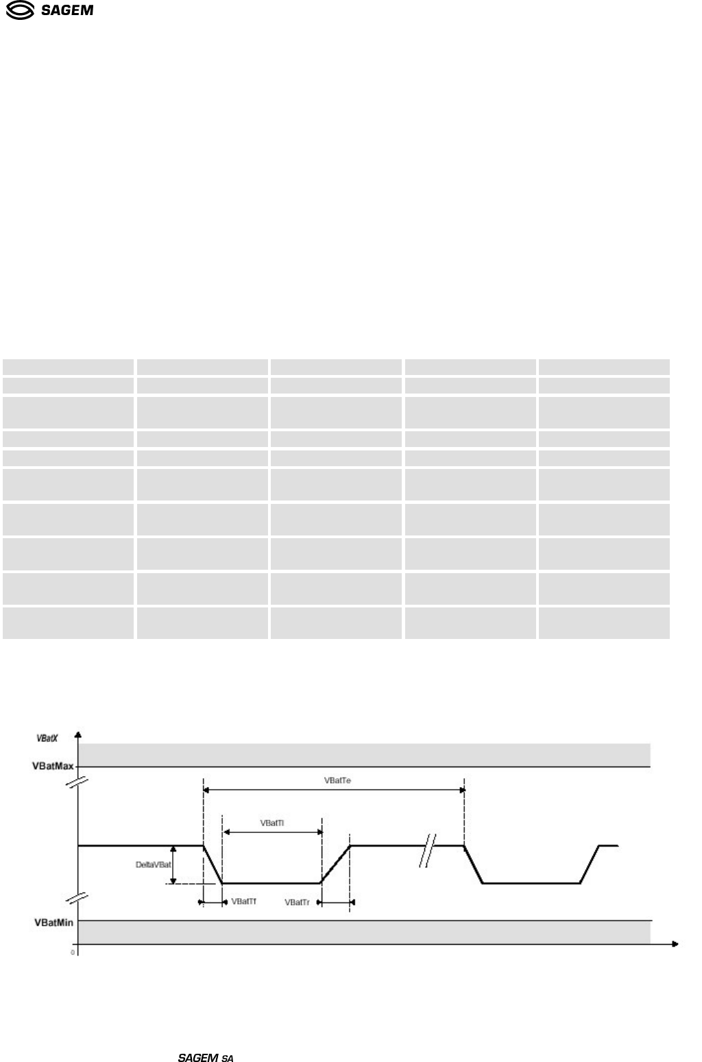
The module is supplied through the VBAT signal with the following characteristics:
Parameter Name Min Typ Max
VBAT period (ms) VbatTe (*) 4.614 4.615 DC
VBAT low duration
(us) VbatTi (*) 550 - VBAT period
VBAT rise time (us) VbatTr (*) 0 - -
VBAT fall time (us) VbatTf (*) 0 - -
VBAT maximum
voltage (V) VbatMax (*) - - 4.5
VBAT minimum
voltage (V) VbatMin (*) 3.45 - -
VBAT drop voltage
(mV) DeltaVbat (*) - - 450 (**)
Transient voltage
(V) 3 - -
Noise level (Vrms)
@100MHz-1MHz - - 50mV
(*): cf figure 8.
(**): for a new battery. Of course for an old battery, this value will be higher and will create a reset (without MMI
message) of the modul when the battery begins to be discharged.
Figure 4
VBAT voltage waveform
Ref : SCT TMO MOD SPEC 662
Rev.: B
Ref. sec. :
Date: 18/11/2004
Document . All rights of reproduction and disclosure reserved.
MO2XX module – Confidential under NDA Page 31/67
6.2 VRIO
Signal Min Typ Max Remarks
Voltage level (activ
mode) 2.70V 2.80V 2.90V
Voltage level (sleep
mode) 2.70V 2.80V 3.00V
Current capability
Active mode - - 10mA
Current capability
Sleep mode - - 0.5mA
Rise time -10µs-
6.3 DAI INTERFACE
DAIRST, DAIIN, DAICLK and DAIOUT have the following characteristics:
VL (V) VH (V)Signal
Min Max Min Max
Remarks
DAIRST -0.5 +0.8 +2.03 +3.2
DAICLK -0.5 +0.8 +2.03 +3.2 PD 100K
DAIIN -0.5 +0.8 +2.03 +3.2 PD 100K
DAIOUT - +0.59 +2.32 -
6.4 NETWORK LED
LEDR and LEDG have the following characteristics:
VL (V) VH (V)Signal
Min Max Min Max
Remarks
State after RESET
LEDR (out) - -
To be verified
LEDG (out) - -
To be verified
6.5 SERIAL INTERFACE (µWIRE)
DIMIW, DOMIW, CKMIW, CSMIW1* have the following characteristics:
VL (V) VH (V)Signal
Min Max Min Max
Remarks
DIMIW -0.5 +0.8 +2.03 +3.2 PU 100K
DOMIW - +0.59 +2.32 -
CKMIW - +0.59 +2.32 -
CSMIW1* - +0.59 +2.32 -
6.6 SIM
VL (V) VH (V)Signal
Min Max Min Max
Remarks
State after RESET
SIMRST
SIMCLK
SIMIO
SIMVCC
SIMCD
Fully compliant to the GSM11.11 and
ISO/IEC 7816-3 standards
Fully
compliant to
the GSM11.11
and ISO/IEC
7816-3
standards. PD
Ref : SCT TMO MOD SPEC 662
Rev.: B
Ref. sec. :
Date: 18/11/2004
Document . All rights of reproduction and disclosure reserved.
MO2XX module – Confidential under NDA Page 32/67
6.7 V24 (UART 1)
TXD,RXD,CTS, RTS, DCD, DSR, DTR and RI have the following characteristics:
VL (V) VH (V)
Remarks
State after resetSignal
Min Max Min Max
RTS -0.5 +0.8 +2.03 +3.2
PU 100K
RI - +0.59 +2.32 -
CTS - +0.59 +2.32 -
DSR - +0.59 +2.32 - PD
DCD - +0.59 +2.32 - PU 10K
DTR -0.5 +0.8 +2.03 +3.2
PU 100K
TXD1 - +0.59 +2.32 -
RXD1 -0.5 +0.8 +2.03 +3.2 PU 10K
6.8 UART2
TXD2 and RXD2 have the following characteristics:
VL (V) VH (V)Signal
Min Max Min Max
Remarks
State after RESET
RXD2 -0.5 +0.8 +2.03 +3.2 PU 100K
TXD2 - +0.59 +2.32 -
6.9 DATA / COMMAND MULTIPLEXING
MOD_ESCAPE*_CMD and DTE_ESCAPE*_CMD have the following characteristics:
VL (V) VH (V) Remarks State after resetSignal
Min Max Min Max
MOD_ESCAPE*_CMD
-0.5 +0.8 +2.03 +3.2 ESD
protection
PU
DTE_ESCAPE_CMD - +0.59 +2.32 -ESD
protection
Ref : SCT TMO MOD SPEC 662
Rev.: B
Ref. sec. :
Date: 18/11/2004
Document . All rights of reproduction and disclosure reserved.
MO2XX module – Confidential under NDA Page 33/67
6.10 POWER MANAGEMENT
They have the following characteristics:
VL (V) VH (V)Signal
Min Max Min Max
Remarks State after RESET
MOD_RESET_STATE,
MOD_UART_STATE,
MOD_FLOW_STATE,
MOD_ON_STATE
- +0.59 +2.32 -ESD protection
PD 100K
MOD_ON*_CMD -
0.3*VBAT
0.7*VBAT
- PU
Ton min: 33 ms
DTE_UART*_STATE -0.5 +0.8 +2.03 +3.2 Prog PU
DTE_RESET*_CMD - +0.59 +2.32 -
MOD_OFF*_CMD -0.5 +0.8 +2.03 +3.2 PU
Pulse duration in
functional mode:
77ns min.
6.11 AUDIO SIGNALS
Audio Inputs
Parameter Tests Conditions Min Typ Max Units
Maximum input range
(MICIP-MICIN) Inputs 3 dBm0 (Maximum digital sample
amplitude with PGA gain set to 0dB) 32.5 mVrms
Maximum Input Range
(HSMIC-AUXI)
Inputs 3 dBm0 (Maximum digital sample
amplitude with PGA gain set to 0dB),
HSDIF = 1 32.5 mVrms
Nominal reference level
(MICIP-MICIN) -10 dBm0
Nominal reference level
at (HSMIC-AUXI) HSDIF = 1 -10 dBm0
Differential input
resistance (MICIP-
MICIN) HSDIF = 0 36
Differential input
resistance (HSMIC-
AUXI) HSDIF = 1 36
Micro amplifier gain
(MICIP- MICIN) HSDIF = 0 25.6 dB
Micro amplifier gain
(HSMIC - AUXI) HSDIF = 1 25.6 dB
Audio Outputs
Ref : SCT TMO MOD SPEC 662
Rev.: B
Ref. sec. :
Date: 18/11/2004
Document . All rights of reproduction and disclosure reserved.
MO2XX module – Confidential under NDA Page 34/67
Parameter Tests Conditions
Min Typ Max
Units
Output swing 3.9 Vpp 120
Differential Minimum resistive load
between HPP32 and HPN32 ; R// Output swing 1.5 Vpp 33
Differential Maximum capacitor
load between HPP32 and HPN32;
C//
100
pF
Common mode Minimum resistive
load at HPP32 and HPN32 200 k
Common mode Maximum load at
HPP32 and HPN32
10
pF
Minimum resistive load at HSOL
and HSOR: R// 32
Maximum capacitor load at HSOL
and HSOR: C//
100
pF
Differential Minimum resistive load
between HPP8 and HPN8: R// Output swing 4.38 Vpp 8
Differential Maximum capacitor
load between HPP8 and HPN8:
C//
100
pF
Common mode Minimum resistive
load at HPP8 and HPN8 200
Common mode Maximum
capacitor load at HPP8 and HPN8
10
pF
Global Characteristics
Parameter Tests Conditions
Min Typ Max
Units
Distortion ≤3.1 3.92
Earphone Maximum output
swing at HPP32 - HPN32 Distortion ≤
5.34dBm0 1.2 1.5 Vpp
Earphone amplifier gain 1 dB
Headphone Maximum output
swing at (HSOL/R) Distortion ≤1.6 1.96 Vpp
Headphone L/R amplifier gain -5 dB
Distortion ≤
Pout=340mW, SPKG = 0 3.73 4.66
Distortion ≤
Pout=380mW, SPKG = 1, VMIDSEL=1,
VSP input level=-2.5dBm0 3.96 4.95Speaker maximum output at
HPP8 - HPN8
Distortion ≤
Pout=430mW, SPKG = 1, VMIDSEL=1,
VSP input level=-2dBm0 4.2 5.24
Vpp
Speaker amplifier gain SPKG=0
SPKG=1 2.5
8.5 dB
6.12 CHARGER
Charger has the following characteristics:
Parameter Description MIN Max
VCHARGEUR Charger voltage 6V 7V
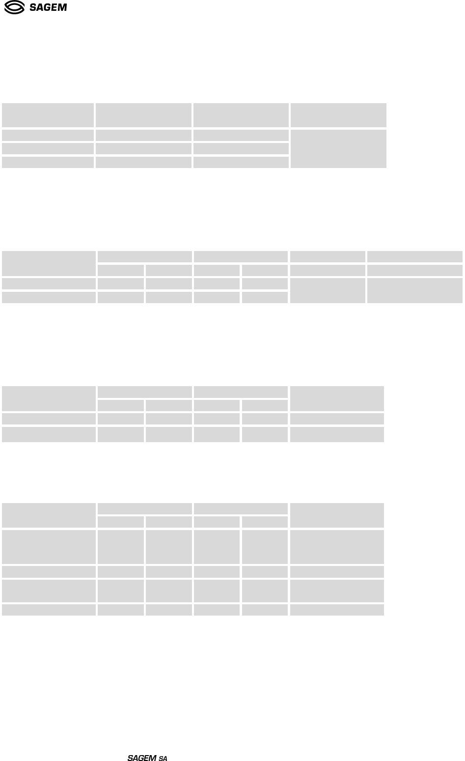
See details on Application Note
Ref : SCT TMO MOD SPEC 662
Rev.: B
Ref. sec. :
Date: 18/11/2004
Document . All rights of reproduction and disclosure reserved.
MO2XX module – Confidential under NDA Page 35/67
6.13 RESET
MOD_RESET*_CMD is active at low state
It has the following characteristics:
Signal Min Max Remarks
VL (V) - 0.3 VBAT
VH (V) 0.7 VBAT -
Treset (ms) 65 -
Electrical levels TBC
NB: The reset signal resets all the system including backup.
6.14 SPARE IO
IO5, 6, 7 have the following characteristics:
VL (V) VH (V) Remarks State after RESETSignal
Min Max Min Max
Input -0.5 +0.8 +2.03 +3.2
Output - +0.59 +2.32 -
IO 5,6,7: PD
PU
Iout max = 2mA
6.15 CLOCKS
CLK13M and CLK32K have the following characteristics:
VL (V) VH (V)Signal
Min Max Min Max
Remarks
CLK13M - +0.59 +2.32 -
CLK32K - 0,297 1,32 -
6.16 JTAG INTERFACE
TCLK, TMS, TDI, TDODIGIT, TDIANALOG, BSCAN*, EMU0*, EMU1* have the following characteristics:
VL (V) VH (V)Signal
Min Max Min Max
Remarks
TMS, TDI,
TDIANALOG,
BSCAN*
-0.5 +0.8 +2.03 +3.2 PU
TCK -0.5 +0.8 +2.03 +3.2 PD
TDODIGIT,
TDOANALOG, - +0.59 +2.32 -
EMU0*, EMU1* - +0.59 +2.32 - PU
Ref : SCT TMO MOD SPEC 662
Rev.: B
Ref. sec. :
Date: 18/11/2004
Document . All rights of reproduction and disclosure reserved.
MO2XX module – Confidential under NDA Page 36/67
7. ENVIRONMENTAL SPECIFICATION
Parameter Min Max
Ambient temperature
Normal range -10°C +55°C
Ambient temperature
Extended range -20°C +70°C
Storage temperature -40°C +85°C
Long damp heat
Operating conditions Tested at +60°C, 95% RH during 504 hours
Short damp heat
Storage and
transportation conditions
Tested at +40°C, 95% RH during 96 hours
Normal Range, from -10°c to +55°c:
Inside this normal range, full compliance with GSM standards is guaranteed by SAGEM.
Certification tests reports applies to modules operating in this interval.
Extended Range, from -20°c to -10°c and from +55°c to +70°c:
Inside this extended range, the operability is guaranteed by SAGEM. However, there is not a full certification test
report in this range.
Practically, SAGEM performs non regression tests in this range in order to ensure that the module can attach to the
network and handle a call.
Some performances may remain under the normal GSM expectation (sensitivity, RXlev 1 or 2 dB lower, TX
emitting power slightly weaker).
Out of operational range:
No operation is guaranteed by SAGEM out of the operational range. No operating tests are made below -20°c and
above +70°c.
Ref : SCT TMO MOD SPEC 662
Rev.: B
Ref. sec. :
Date: 18/11/2004
Document . All rights of reproduction and disclosure reserved.
MO2XX module – Confidential under NDA Page 37/67
8. MECHANICAL SPECIFICATION
8.1 PHYSICAL DIMENSIONS
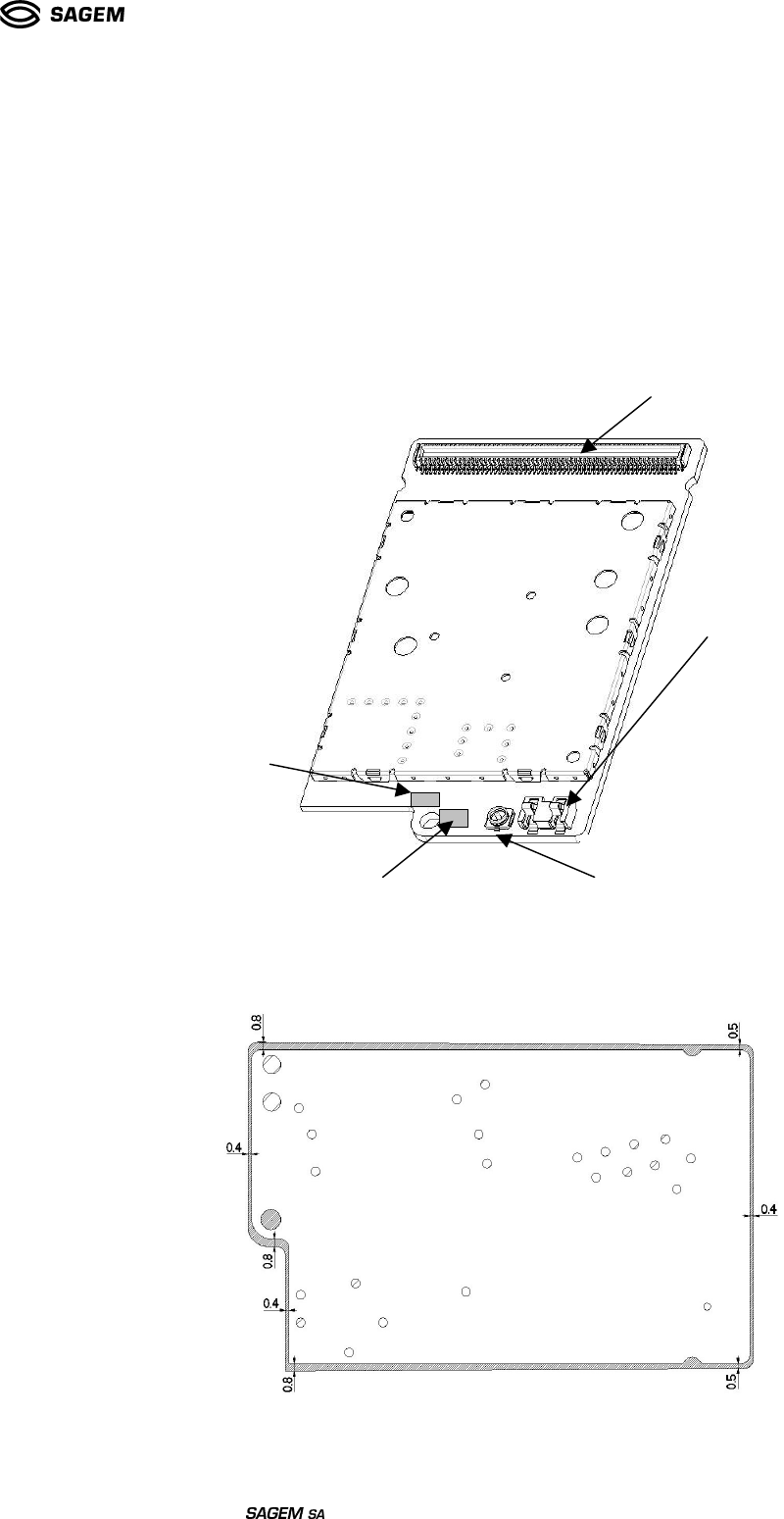
Figure 10
MO2XX
120
1
60
61
AVX Board to Board connector
JST 2 way stacker assembly
Pad for antenna
connection
Murata
coaxial
connection
Ground area
Ref : SCT TMO MOD SPEC 662
Rev.: B
Ref. sec. :
Date: 18/11/2004
Document . All rights of reproduction and disclosure reserved.
MO2XX module – Confidential under NDA Page 38/67
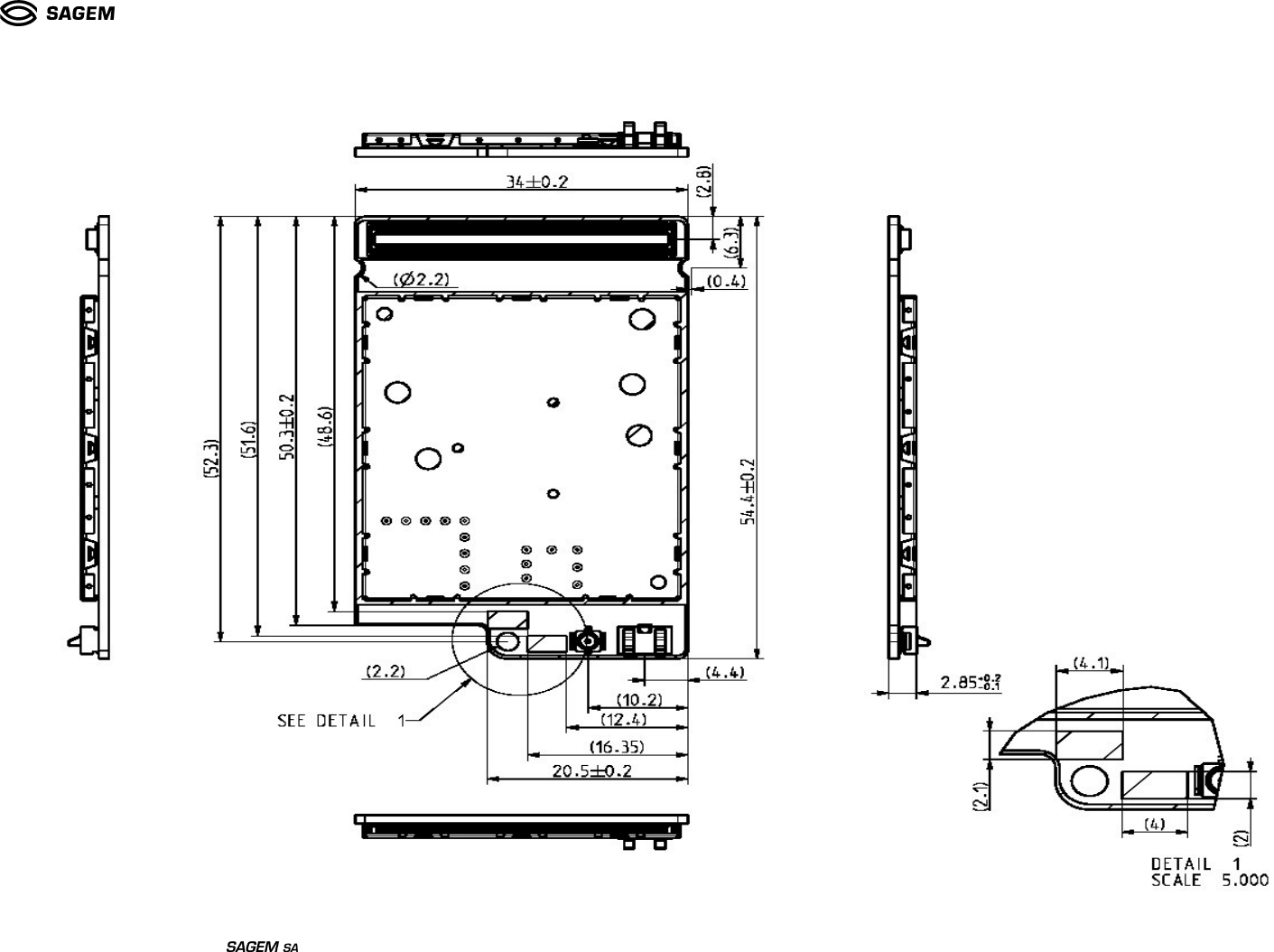
Figure 11
MO2XX dimensions
Ref : SCT TMO MOD SPEC 662
Rev.: B
Ref. sec. :
Date: 18/11/2004
Document . All rights of reproduction and disclosure reserved.
MO2XX module – Confidential under NDA Page 39/67
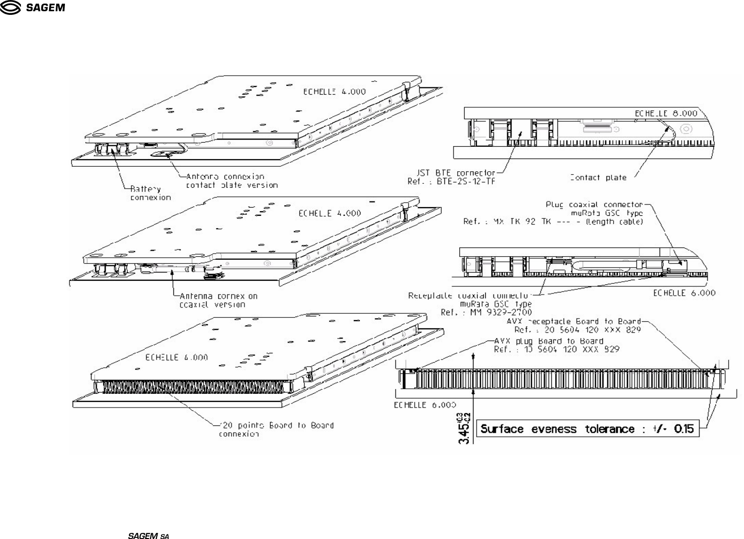
Figure 12
MO2XX connection to a mother board
Ref : SCT TMO MOD SPEC 662
Rev.: B
Ref. sec. :
Date: 18/11/2004
Document . All rights of reproduction and disclosure reserved.
MO2XX module – Confidential under NDA Page 40/67
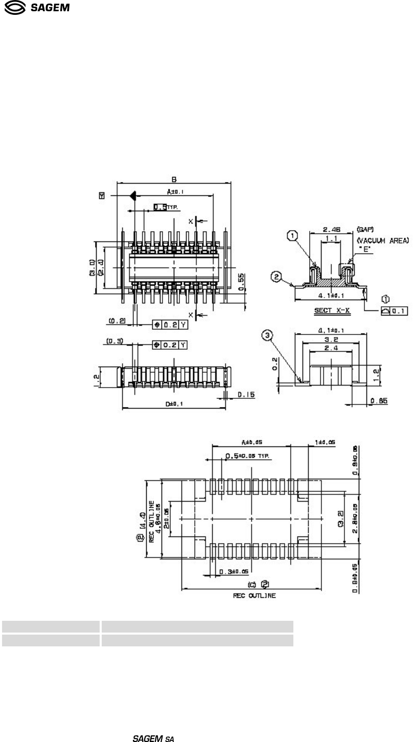
8.2 TERMINAL ASSIGNMENTS
8.2.1. 120 PINS CONNECTOR
8.2.1.1. MO2XX connector
Recommended PC Board Mounting pattern:
Dimensions and references:
Pin Number Reference
120 AVX 10 5604 120 212 829
Ref : SCT TMO MOD SPEC 662
Rev.: B
Ref. sec. :
Date: 18/11/2004
Document . All rights of reproduction and disclosure reserved.
MO2XX module – Confidential under NDA Page 41/67
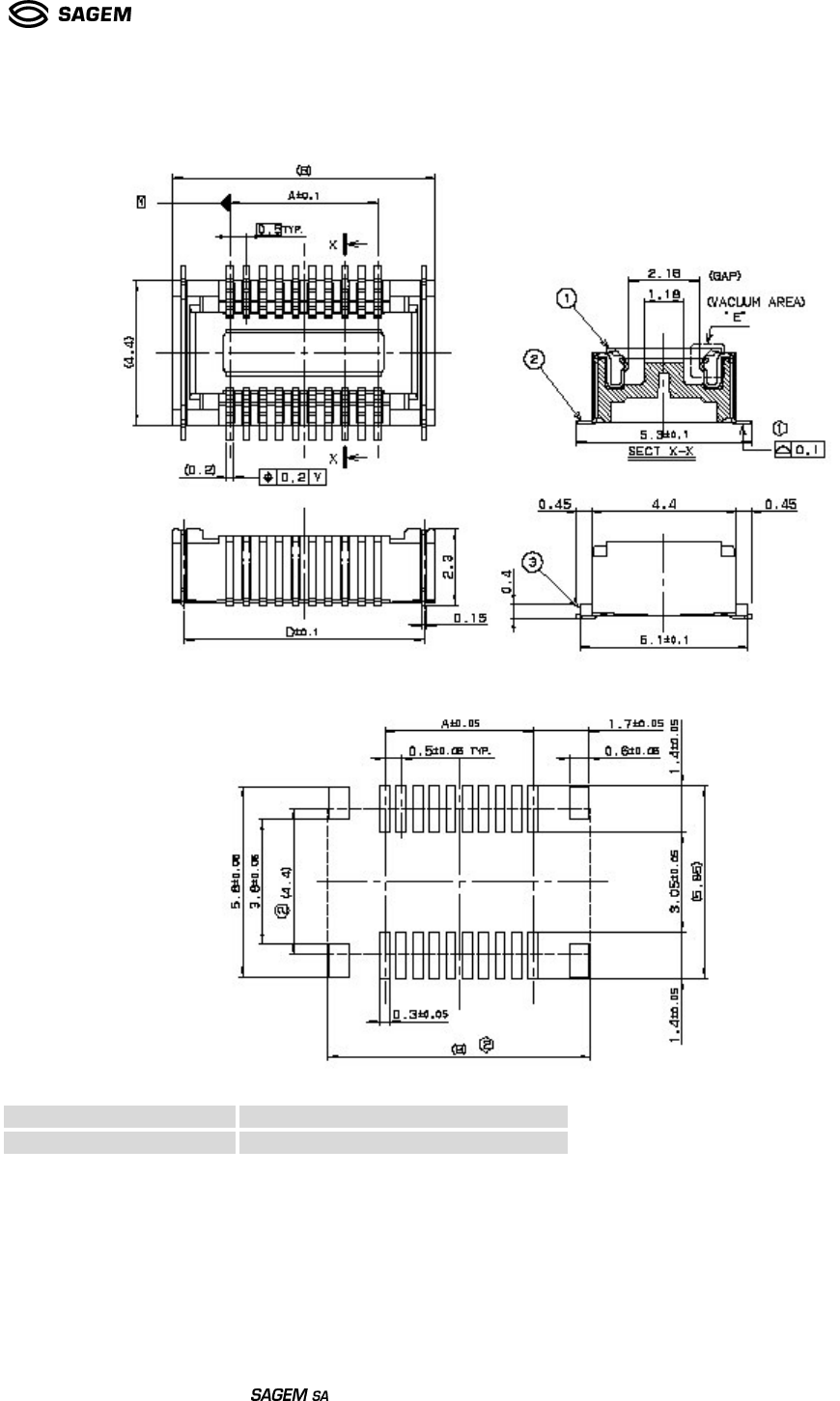
8.2.1.2. Mother board connector
Recommended PC Board Mounting pattern:
Dimensions and references:
Pin Number References
120 AVX 20 5604 120 222 829
Ref : SCT TMO MOD SPEC 662
Rev.: B
Ref. sec. :
Date: 18/11/2004
Document . All rights of reproduction and disclosure reserved.
MO2XX module – Confidential under NDA Page 42/67
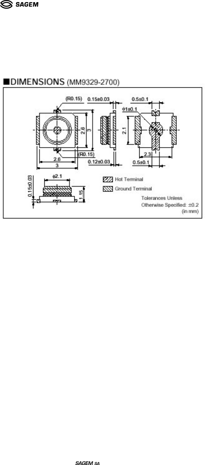
8.2.2. MO2XX ANTENNA CONNECTOR
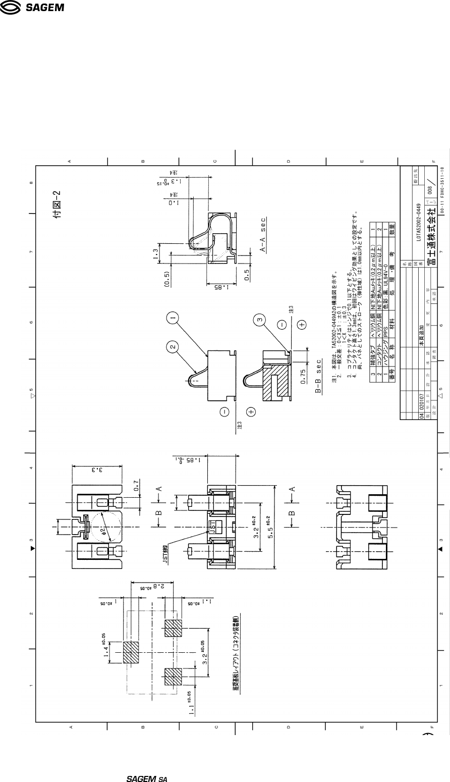
Ref : SCT TMO MOD SPEC 662
Rev.: B
Ref. sec. :
Date: 18/11/2004
Document . All rights of reproduction and disclosure reserved.
MO2XX module – Confidential under NDA Page 43/67
8.2.3. BATTERY CONNECTOR
Ref : SCT TMO MOD SPEC 662
Rev.: B
Ref. sec. :
Date: 18/11/2004
Document . All rights of reproduction and disclosure reserved.
MO2XX module – Confidential under NDA Page 44/67
ANNEX 1 : IO description
IO name Type Pin N°
DAIRST Digital bi directional buffer (IDI041/OUK431) 116
DAIOUT Digital bi directional buffer (IDI041/OUK431) 115
DAIIN Digital bi directional buffer (IDI041/OUK431). Pull down 117
DAICLK Digital bi directional buffer (IDI041/OUI431). Pull down 118
USL1 Digital input buffer (IDI041/PS0201)
USL2 Digital output buffer (OUK431)
USL3 Digital output buffer (OUI431)
USL4 Digital output buffer (OUK431)
USL5 Digital output buffer (OUK431)
USL6 Digital bi directional buffer (IDG091/OUI431/PE1001)
USL7 Digital bi directional buffer (IDI041/OUI431/PS1001)
USL8 Digital bi directional buffer (IDI041/OUI431/PS1001)
USL9 Digital bi directional buffer (IDI041/OUI431/PS1001)
USL10 Digital bi directional buffer (IDI041/OUI431/PS1001)
MOD_ESCAPE*_CMD Digital bi directional buffer (IDI041/OUI431/PS1001) 18
USL11 Digital bi directional buffer (IDI041/OUI431/PS1001)
USL12 Digital output buffer (OUO431)
DTE_ESCAPE_CMD Digital output buffer (OUI431) 23
MOD_RESET_STATE Digital output buffer (OUI431) 24
MOD_UART_STATE Digital output buffer (OUI431) 25
MOD_FLOW_STATE Digital output buffer (OUI431) 26
MOD_ON_STATE Digital output buffer (OUI431) 27
MOD_ON*_CMD Digital input 113
SIMVCC Power supply output 6
SIMRST Digital output buffer 5
SIMCLK Digital output buffer 4
SIMIO Digital bi directional buffer 7
SIMCD Digital input buffer (IDI091) 114
HSMICIP Analog audio input 52
HSMICIN Analog audio input 53
HSOL Analog audio output 50
HSOR Analog audio output 49
MICIP Analog audio input 63
MICIN Analog audio input 62
HPP32 Analog audio output 46
HPN32 Analog audio output 47
HPP8 Analog audio output 56
HPN8 Analog audio output 57
USL13 Digital bi directional buffer (IDG091/OUI431/PE1001)
RI Digital bi directional buffer (IDG091/OUO431/PS1001) 109
DSR Digital bi directional buffer (IDG091/OUI431/PE1001) 94
DCD Digital output buffer (OUI831) 110
DTR Digital bi directional buffer (IDI091/OUI831) 95
CTS Digital output buffer (OUI831) 82
RTS Digital bi directional buffer (IDI091/OUO431) 83

Ref : SCT TMO MOD SPEC 662
Rev.: B
Ref. sec. :
Date: 18/11/2004
Document . All rights of reproduction and disclosure reserved.
MO2XX module – Confidential under NDA Page 45/67
TXD1 Digital output buffer (OUI831) 101
RXD1 Digital bi directional buffer (IDI091/OUI831) 105
TXD2 Digital output buffer (OUI831) 103
RXD2 Digital input buffer (IDI091) 104
TXIR Digital bi directional buffer (IDI041/OUI831)
RXIR Digital bi directional buffer (IDI091/OUK431)
CMDIRDA Digital output buffer (OUK431)
USL14 Digital bi directional buffer (IDG091/OUI431/PS1001)
USL15 Digital bi directional buffer (IDI091/UOS205)
USL16 Digital bi directional buffer (IDI091/UOS205)
DTE_UART*_STATE Digital bi directional buffer (IDG091/OUI431/PS1001) 92
CHARGEUR Power supply input 69, 70
LEDC Analog output
MOD_RESET*_CMD Digital input 81
MOD_OFF*_CMD Digital bi directional buffer (IDI091/OUI431/PS1001) 76
USL17 Digital bi directional buffer (IDI041/OUI831)
USL18 Digital bi directional buffer (IDI041/OUI831)
USL19 Digital bi directional buffer (IDI041/OUI831)
USL20 Digital bi directional buffer (IDI041/OUI831)
USL21 Digital bi directional buffer (IDI041/OUI831)
USL22 Digital bi directional buffer (IDI041/OUI831)
USL23 Digital bi directional buffer (IDI041/OUI831)
USL24 Digital bi directional buffer (IDI041/OUI831)
USL25 Digital bi directional buffer (IDI041/OUI831)
USL26 Digital bi directional buffer (IDI041/OUI831)
USL27 Digital bi directional buffer (IDI041/OUI831)
USL28 Digital bi directional buffer (IDI041/OUI831)
USL29 Digital bi directional buffer (IDI041/OUI831)
USL30 Digital bi directional buffer (IDI041/OUI831)
USL31 Digital bi directional buffer (IDI041/OUI831)
USL32 Digital bi directional buffer (IDI041/OUI831)
USL33 Digital bi directional buffer (IDI041/OUI831)
USL34 Digital output buffer (OUI831)
USL35 Digital bi directional buffer (IDI041/OUI831)
USL36 Digital bi directional buffer (IDI041/OUI831)
USL37 Digital bi directional buffer (IDI041/OUI831)
USL38 Digital bi directional buffer (IDI041/OUI831)
USL39 Digital bi directional buffer (IDI041/OUI431)
USL40 Digital bi directional buffer (IDI041/OUI431)
USL41 Digital bi directional buffer (IDI041/OUI431)
USL42 Digital bi directional buffer (IDI041/OUI431)
USL43 Digital bi directional buffer (IDI041/OUI431)
USL44 Digital bi directional buffer (IDI041/OUI431)
USL45 Digital bi directional buffer (IDI041/OUI431)
USL46 Digital bi directional buffer (IDI041/OUI431)
USL47 Digital output buffer (OUI431)
USL48 Digital output buffer (OUI431)
USL49 Digital output buffer (OUI431)
USL50 Digital output buffer (OUI431)
USL51 Digital output buffer (OUI431)
Ref : SCT TMO MOD SPEC 662
Rev.: B
Ref. sec. :
Date: 18/11/2004
Document . All rights of reproduction and disclosure reserved.
MO2XX module – Confidential under NDA Page 46/67
DTE_RESET*_CMD Digital output buffer (OUI431) 106
USL52 Digital bi directional buffer (UIS245/UOS181)
USL53 Digital bi directional buffer (UIS245/UOS181)
USL54 Power supply input
USL55 Digital output buffer (OUI831)
USL56 Digital bi directional buffer (IDG091/OUM431/PE0201)
USL57 Digital bi directional buffer (IDG091/OUI831)
USL58 Digital output buffer (IDG091)
USL59 Digital input buffer (OUM431)
USL60 Digital output buffer (OUI431)
USL61 Digital bi directional buffer (IDI041/OUI431)
USL62 Digital bi directional buffer (IDI041/OUI431)
USL63 Digital bi directional buffer (IDI041/OUI431)
USL64 Digital bi directional buffer (IDI041/OUI431)
USL65 Digital bi directional buffer (IDI041/OUI431)
USL66 Digital bi directional buffer (IDI041/OUI431)
USL67 Digital bi directional buffer (IDI041/OUI431)
USL68 Digital bi directional buffer (IDI041/OUI431)
USL69 Digital bi directional buffer (IDG091/OUI431/PE1001)
USL70 Digital bi directional buffer (IDG091/OUI431/PS1001)
USL71 Digital bi directional buffer (IDG091/OUI431/PS1001)
USL72 Digital bi directional buffer (IDG091/OUO431/PS1001)
USL73 Digital bi directional buffer (IDG091/OUI431/PS1001)
USL74 Digital bi directional buffer (IDI091/OUI831/PS1001)
USL75 Digital output buffer (OUI431)
USL76 Digital output buffer (OUI431)
USL77 Digital output buffer (OUI431)
USL78 Digital output buffer (OUI431)
USL79 Digital output buffer (OUI431)
USL80 Digital bi directional buffer (IDI041/OUI431)
USL81 Digital output buffer (OUI431)
USL82 Digital bi directional buffer (IDG091/OUM431/PS0201)
USL83 Digital bi directional buffer (IDG091/OUM431/PS0201)
USL84 Digital bi directional buffer (IDG091/OUM431/PS0201)
USL85 Digital bi directional buffer (IDG091/OUM431/PS0201)
USL86 Digital bi directional buffer (IDG091/OUI431)
USL87 Digital output buffer (OUI431)
USL88 Digital bi directional buffer (IDG091/OUM431/PS1001)
CLK13M Digital bi directional buffer (IDI041/OUI831) 16
CLK32K Digital output buffer (OUK431) 9
ADC2 Analog input 11
USL90 Digital input buffer (IDG091)
USL91 Digital output buffer (OUM431)
USL92 Digital bi directional buffer (IDG091/OUM431)
USL93 Digital bi directional buffer (IDG091/OUM431)
IO5 Digital bi directional buffer (IDG091/OUI431/PE1001) 80
IO6 Digital bi directional buffer (IDG091/OUI431/PE1001) 65
IO7 Digital bi directional buffer (IDG091/OUI431/PS1001) 107
LEDR Digital output buffer (OUI831) 91
LEDG Digital output buffer (OUK431) 90
Ref : SCT TMO MOD SPEC 662
Rev.: B
Ref. sec. :
Date: 18/11/2004
Document . All rights of reproduction and disclosure reserved.
MO2XX module – Confidential under NDA Page 47/67
VBAT Power supply input Bat Con
1,2
VRIO Power supply output 2
VBACKUP Power supply input 12
ANTENNE Analog bi directional HF Ant
TCK Digital input buffer (IDI091/ PE0201) Test point
TMS Digital input buffer (IDI091/ PS0201) Test point
TDIDIGIT Digital input buffer (IDI091/ PS0201) Test point
TDODIGIT Digital bi directional buffer (OUI431) Test point
TDIANALOG Digital bi directional buffer Test point
TDOANALOG Digital bi directional buffer Test point
BSCAN* Digital input buffer (IDI041/ PS0201) Test point
EMU0* Digital bi directional buffer (IDI091/OUO431/PS1001) Test point
EMU1* Digital bi directional buffer (IDI091/OUO431/PS1001) Test point
OUO231 : rated output current = 1mA (with Voh = Vccmin)
OUI431, OUK431, OUO431 :rated output current = 2mA (with Voh = Vccmin)
OUI831, OUK831 : rated output current = 4mA (with Voh = Vccmin)
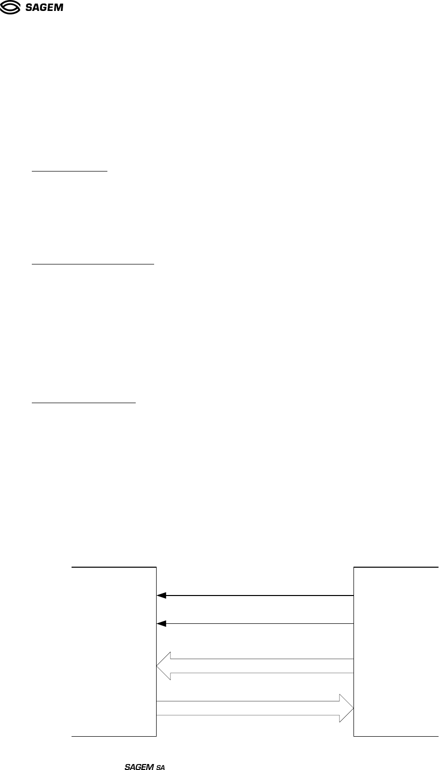
Ref : SCT TMO MOD SPEC 662
Rev.: B
Ref. sec. :
Date: 18/11/2004
Document . All rights of reproduction and disclosure reserved.
MO2XX module – Confidential under NDA Page 48/67
ANNEX 2 : Hardware power management
Different strategies
The transition of the MO2XX from awake to asleep can be managed in 4 different ways:
• Inhibition by DTE:
The DTE can forbid the MO2XX to go to sleep. But if it is allowed to sleep, it do it when it wants and without
informing the DTE.
This allows a very simple management by the DTE but should be used when the power management is not
a critical issue. In this case, the DTE only handles the ON and OFF states without any requirement.
• Management by DCE alone:
The MO2XX goes to sleep on its own decision and the DTE can't forbid it. The DTE doesn't know the state
of the MO2XX.
This is the most common case because it allows to reduce the module’s consumption without requiring
special treatments on the host side. In this case, the host uses the UART capabilities to wake up on a byte
reception (*).
(*): The first byte may be lost by the module
• Hardware management:
The transition to sleep state is done only when the 2 equipments agree. So each one knows the state of
the other.
This solution allows to switch off the serial link on both side and so to save as much battery life as possible;
it is strongly recommended when the battery life is a critical issue.
Details are given in the following chapters.
1. Interface specification.
1.1 Management by DCE alone.
MO190
DTE
TX
RX
RTS
DTR
MO2XX
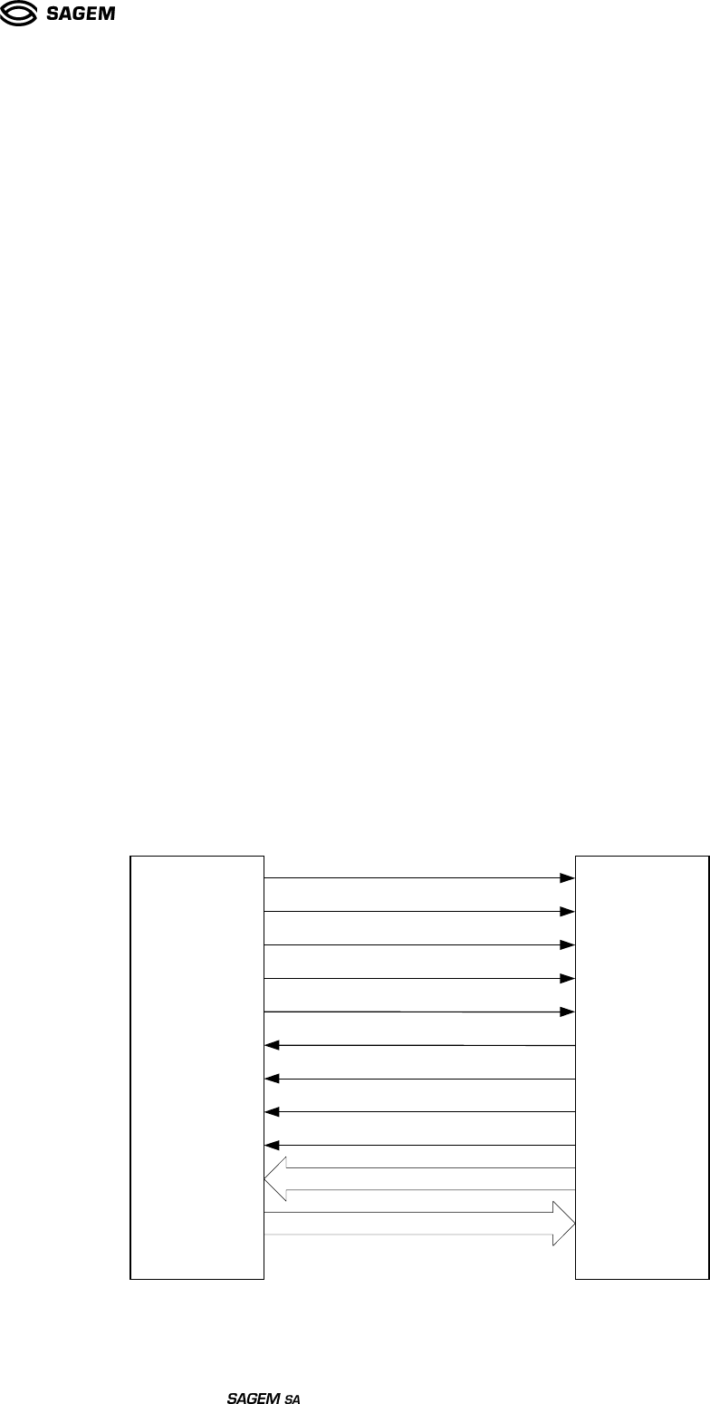
Ref : SCT TMO MOD SPEC 662
Rev.: B
Ref. sec. :
Date: 18/11/2004
Document . All rights of reproduction and disclosure reserved.
MO2XX module – Confidential under NDA Page 49/67
When the UART of the MO2XX doesn't detect any activity on the RX input during a certain time, it allows
the MO2XX to switch off the UART when it wants. The DTE doesn't know when the MO2XX switches its
UART off.
If the DTE sends data to the MO2XX when the UART is off, the first character will wake up the DCE and
the first byte may be lost. Another way for the DTE to wake up the MO2XX is to put down its DTR or RTS.
1.2 Inhibition by DTE.
It is the same management as in 1.1 except that as long as the DTE has its DTR active, the MO2XX is
not allowed to switch off the UART anymore.
1.3 Hardware management.
This management uses signals to inform each equipment of the state of the other one. Signals are also
used to request a change of state of the other.
This methods allows to achieve a lower power consumption of the device by switching off the interface
modules as often as possible (i.e. when no communication is needed).
1.3.1. Signals.
There are 5 outputs and 4 inputs used to control the different states:
Output: MOD_ON_STATE, DTE_RESET*_CMD, MOD_UART_STATE, MOD_FLOW_STATE and
MOD_RESET_STATE.
Inputs: MOD_ON*_CMD, MOD_RESET*_CMD, DTE_UART*_STATE, MOD_OFF*_CMD.
As for now, the DTE_RESET*_CMD is not actually controlled by the MO2XX. It is just provided as a
spare in case the DTE needs a reset command from the DCE (very unlikely).
MOD_ON_STATE
MOD_UART_STATE
MOD_FLOW_STATE
MOD_RESET_STATE
MOD_OFF*_CMD
DTE_UART*_STATE
MOD_RESET*_CMD
MOD_ON*_CMD
RX
TX
DTE_RESET*_CMD
MO2xx
DTE
MOD_ON_STATE is active when the MO2XX is ON.
MOD_UART_STATE is inactive when the MO2XX is in deep sleep.
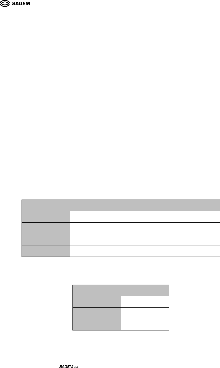
Ref : SCT TMO MOD SPEC 662
Rev.: B
Ref. sec. :
Date: 18/11/2004
Document . All rights of reproduction and disclosure reserved.
MO2XX module – Confidential under NDA Page 50/67
MOD_FLOW_STATE is inactive when the MO2XX has nothing to send.
MOD_RESET_STATE is active during the the software reset procedure, but it can not be trusted
during hardware reset.
MOD_OFF*_CMD command the switch off of the MO2XX.
MOD_ON*_CMD command the switch on of the MO2XX.
DTE_UART*_STATE is inactive when the DTE has nothing to send. If MOD_FLOW_STATE is
inactive too, the DTE can switch off its UART.
MOD_RESET*_CMD command the reset of the DCE.
To make an interface with a host, the XS200 power management and hardware multiplexing
signals need to be polarized with pull down or pull up resistors :
Power management inputs :
DTE_UART*_STATE need pull up resistors (100K).
1.3.2. Signals and states.
In these tables as well as in the following chapters, we will consider the logical levels (active,
inactive or either) and not the actual electric one (high, low ...).
• MO2XX modes:
Each state is represented by the combination of MOD_ON_STATE and MOD_UART_STATE
signals.
MOD_ON_STATE
MOD_UART_STATE
MOD_RESET_STATE
OFF Inactive Inactive Inactive
ON Sleep Active Inactive Inactive
ON Active Active Active Inactive
RESET Active Either Active
• DTE modes:
The DCE only needs to know if the serial link of the DTE is active or not. It is represented by the
DTE_UART_STATE signal.
DTE_UART_STATE
OFF Inactive
ON Sleep Inactive
ON Active Active
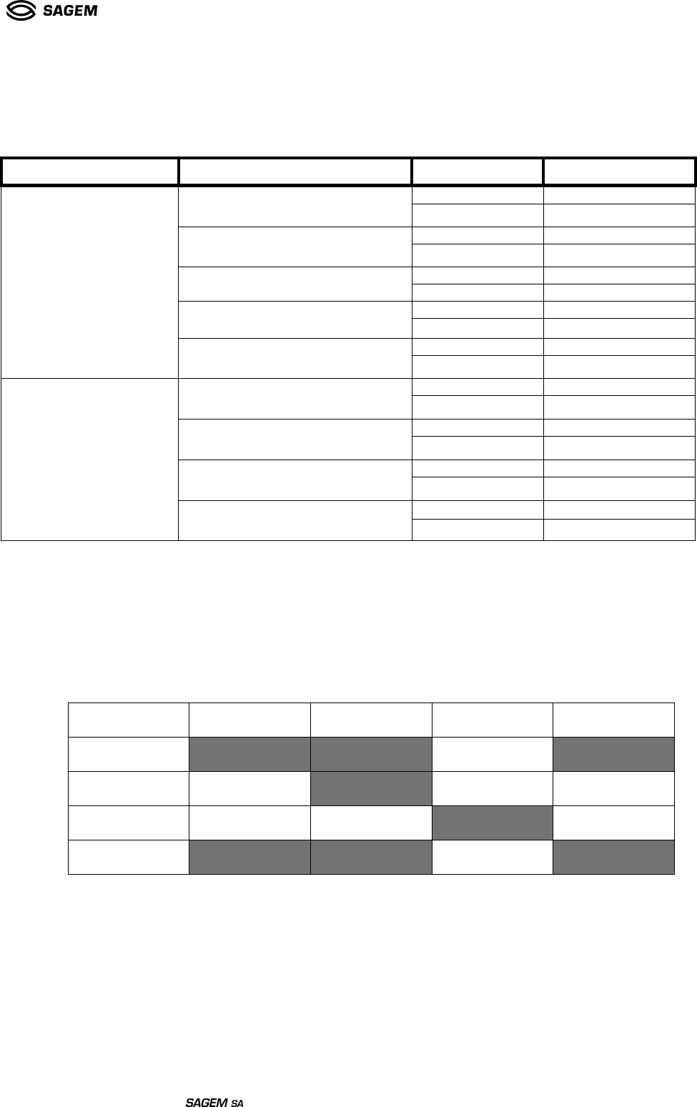
Ref : SCT TMO MOD SPEC 662
Rev.: B
Ref. sec. :
Date: 18/11/2004
Document . All rights of reproduction and disclosure reserved.
MO2XX module – Confidential under NDA Page 51/67
Logical and electrical levels:
Signal Logical levels Electrical levels
Active Low level
DTE_RESET*_CMD Inactive High level
Active High level
MOD_ON_STATE Inactive Low level
Active High level
MOD_UART_STATE Inactive Low level
Active High level
MOD_FLOW_STATE Inactive Low level
Active High level
MO2XX output
MOD_RESET_STATE Inactive Low level
Active Low level
MOD_OFF*_CMD Inactive High level
Active Low level
MOD_ON*_CMD Inactive High level
Active Low level
DTE_UART*_STATE Inactive High level
Active Low level
MO2XX input
MOD_RESET*_CMD Inactive Low level
1.3.3. Communication protocols.
1.3.3.1. Transition tables.
This table lists the possible transition of the DCE from one state to another and which equipment can
initiate the change.
Initial Final OFF ON Sleep ON Active RESET
OFF Impossible DTE Impossible
ON Sleep DTE DCE/DTE DCE/DTE
ON Active DTE DTE/DCE DCE/DTE
RESET X Impossible X
1.3.3.2. Command signals.
A logical rising edge on MOD_ON_CMD means that the DTE wants the DCE to go ON.
A logical rising edge on MOD_OFF_CMD means that the DTE wants the DCE to go OFF.
A logical falling edge on DTE_UART_STATE means that the DTE has nothing to send yet.
A logical falling edge on MOD_FLOW_STATE means that the DCE has nothing to send yet.
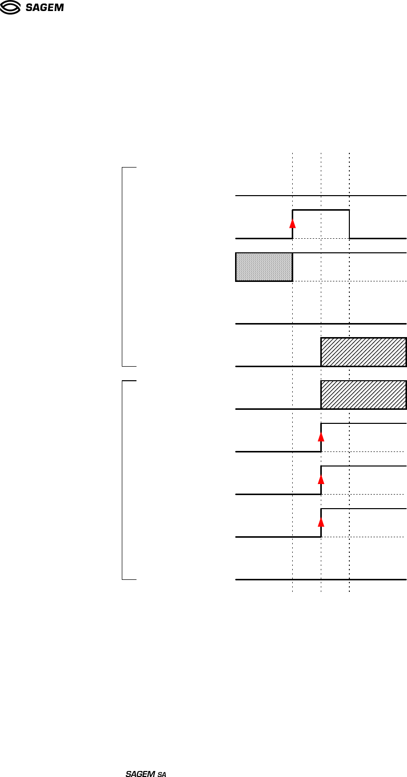
Ref : SCT TMO MOD SPEC 662
Rev.: B
Ref. sec. :
Date: 18/11/2004
Document . All rights of reproduction and disclosure reserved.
MO2XX module – Confidential under NDA Page 52/67
1.3.3.3. Transition from OFF to ON Active.
This transition is only possible by a command from the DTE (the MO2XX never switches off by
itself).
Levels shown on the diagram are logical levels (active, inactive, either)
MOD_ON_CMD
MOD_OFF_CMD
DTE_UART_STATE
MOD_RESET_CMD
MOD_UART_STATE
MOD_ON_STATE
MOD_FLOW_STATE
RX
TX
D
C
E
i
n
p
u
t
s
D
C
E
o
u
t
p
u
t
s
MOD_RESET_STATE
1.3.3.4. Transition from ON Active to ON Sleep.
This transition can be initiated by DCE or DTE.
When an equipment has nothing to send any more, it informs the other. If the other equipment has
nothing to transmit too, they can go to SLEEP state.
The UART of both the equipment's can switch off only when DTE_UART_STATE and
MOD_FLOW_STATE are inactive.
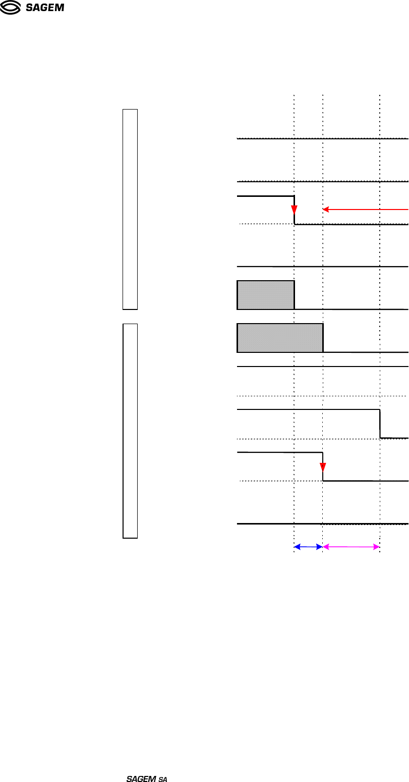
Ref : SCT TMO MOD SPEC 662
Rev.: B
Ref. sec. :
Date: 18/11/2004
Document . All rights of reproduction and disclosure reserved.
MO2XX module – Confidential under NDA Page 53/67
1.3.3.4.1. Initiated by DTE.
MOD_ON_CMD
MOD_OFF_CMD
DTE_UART_STATE
MOD_RESET_CMD
MOD_UART_STATE
MOD_ON_STATE
MOD_FLOW_STATE
RX
D
C
E
i
n
p
u
t
s
UART is OFF
TX
D
C
E
o
u
t
p
u
t
s
MOD_RESET_STATE
state 1
state 2
This transition show 2 transitory states.
During transitory states 1 and 2, the DTE can't send data. If it has to, it must put DTE_UART_STATE
up first.
During transitory state 1, the DTE can receive data and the DCE can send data: there's no problem
for DCE to emit.
During transitory state 2, the DCE can't send data and the DTE can't receive data. So if the DCE
wants to emit, it must put MOD_FLOW_STATE up first.
The state 2 can be long.
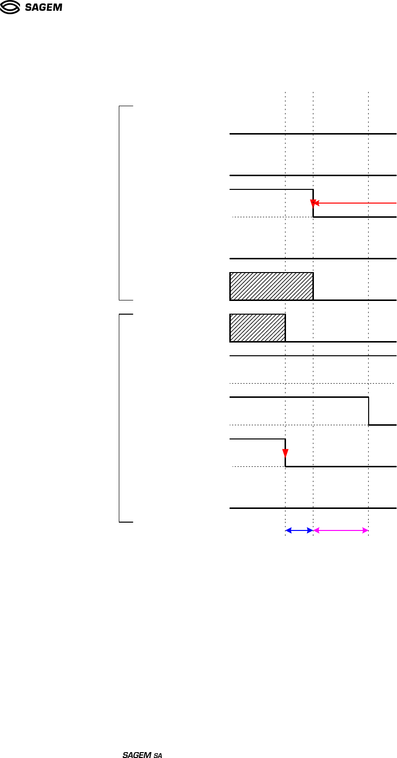
Ref : SCT TMO MOD SPEC 662
Rev.: B
Ref. sec. :
Date: 18/11/2004
Document . All rights of reproduction and disclosure reserved.
MO2XX module – Confidential under NDA Page 54/67
1.3.3.4.2. Initiated by DCE.
MOD_ON_CMD
MOD_OFF_CMD
DTE_UART_STATE
MOD_RESET_CMD
MOD_UART_STATE
MOD_ON_STATE
MOD_FLOW_STATE
RX
TX
D
C
E
i
n
p
u
t
s
D
C
E
o
u
t
p
u
t
s
MOD_RESET_STATE
UART is OFF
state 3
state 2
This transition show 2 transitory states.
During transitory states 2 and 3, the DCE can't send data:
• If it has to during state 2 it must put MOD_FLOW_STATE up (cf. 2.2.3.3.4.3.a) to wake up the
DTE.
• If it has to during state 3 it has to wait for the falling edge of DTE_UART_STATE and then it is
state 2.
During transitory state 3, the DCE can receive data and the DTE can send data: there's no problem
for DTE to emit.
During transitory state 2, the DTE can't send data and the DCE can receive data. So if the DTE
wants to emit, it has just to put DTE_UART_STATE up (cf. 2.2.3.3.4.3.b).
The state 2 can be long.
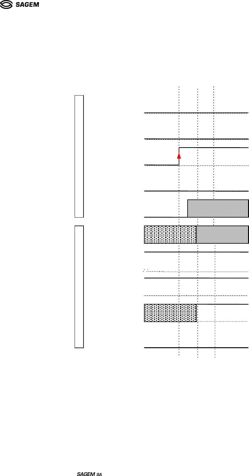
Ref : SCT TMO MOD SPEC 662
Rev.: B
Ref. sec. :
Date: 18/11/2004
Document . All rights of reproduction and disclosure reserved.
MO2XX module – Confidential under NDA Page 55/67
1.3.3.4.3. Transitory states.
a) DTE has data to send:
This case can happen in transitory state 1 and state 2.
MOD_ON_CMD
MOD_OFF_CMD
DTE_UART_STATE
MOD_RESET_CMD
RX
D
C
E
i
n
p
u
t
s
MOD_UART_STATE
MOD_ON_STATE
MOD_FLOW_STATE
TX
D
C
E
o
u
t
p
u
t
s
MOD_RESET_STATE
b) DCE has data to send:
This case can happen in transitory state 2.
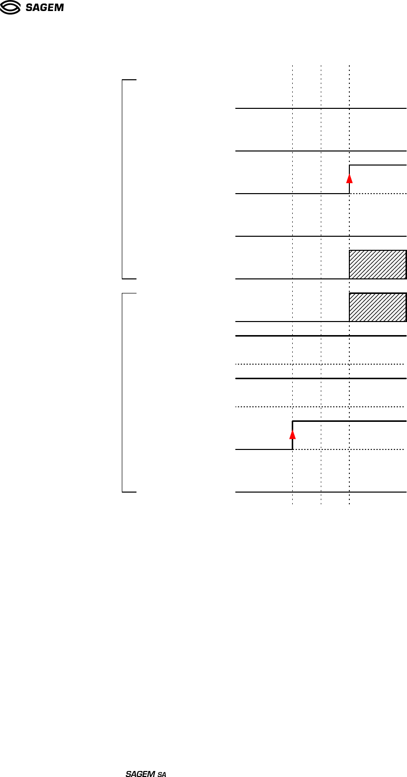
Ref : SCT TMO MOD SPEC 662
Rev.: B
Ref. sec. :
Date: 18/11/2004
Document . All rights of reproduction and disclosure reserved.
MO2XX module – Confidential under NDA Page 56/67
MOD_ON_CMD
MOD_OFF_CMD
DTE_UART_STATE
MOD_RESET_CMD
MOD_UART_STATE
MOD_ON_STATE
MOD_FLOW_STATE
RX
TX
D
C
E
i
n
p
u
t
s
D
C
E
o
u
t
p
u
t
s
MOD_RESET_STATE
1.3.3.5. Transition from ON Sleep to ON Active.
This transition can be initiated by both the DTE and the DCE.
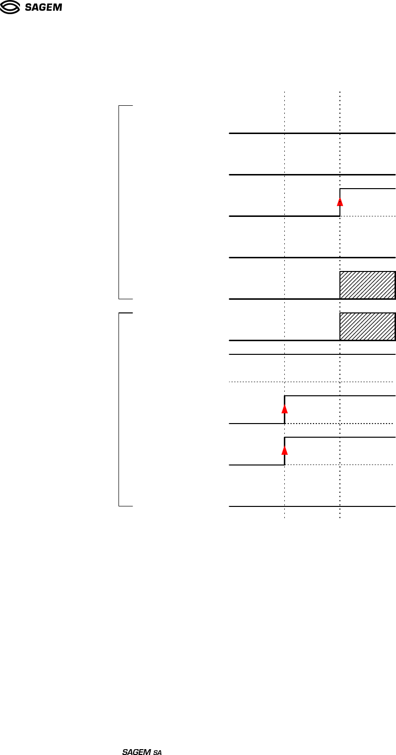
Ref : SCT TMO MOD SPEC 662
Rev.: B
Ref. sec. :
Date: 18/11/2004
Document . All rights of reproduction and disclosure reserved.
MO2XX module – Confidential under NDA Page 57/67
1.3.3.5.1. Initiated by the DCE.
D
C
E
o
u
t
p
u
t
s
D
C
E
i
n
p
u
t
s
MOD_ON_CMD
MOD_OFF_CMD
DTE_UART_STATE
MOD_RESET_CMD
RX
TX
MOD_UART_STATE
MOD_ON_STATE
MOD_FLOW_STATE
MOD_RESET_STATE
1.3.3.5.2. Initiated by DTE.
The DCE can react on the rising edge of the DTE_UART_STATE signal or on the reception of a
character which will be lost. It is only used to wake up the MO2XX.
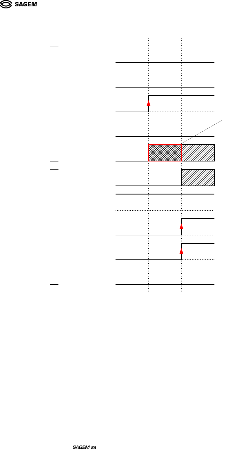
Ref : SCT TMO MOD SPEC 662
Rev.: B
Ref. sec. :
Date: 18/11/2004
Document . All rights of reproduction and disclosure reserved.
MO2XX module – Confidential under NDA Page 58/67
This character is
not mandatory
and will be lost
MOD_ON_CMD
MOD_OFF_CMD
DTE_UART_STATE
MOD_RESET_CMD
RX
TX
MOD_UART_STATE
MOD_ON_STATE
MOD_FLOW_STATE
D
C
E
i
n
p
u
t
s
D
C
E
o
u
t
p
u
t
s
MOD_RESET_STATE
1.3.3.6. Transition from ON Sleep to OFF.
This transition is only possible by a command from the DTE (the MO2XX never switches off by
itself).
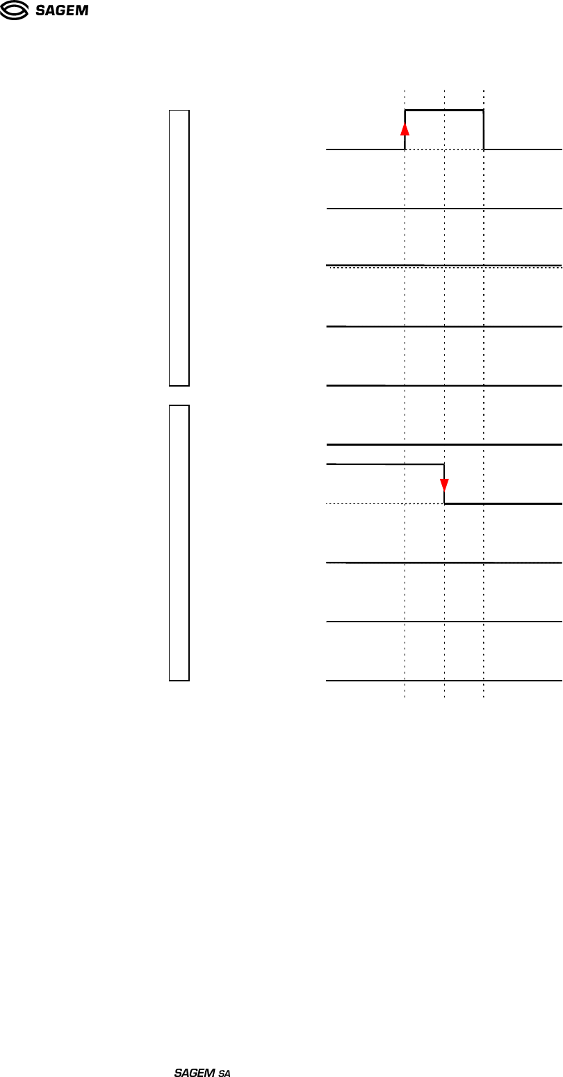
Ref : SCT TMO MOD SPEC 662
Rev.: B
Ref. sec. :
Date: 18/11/2004
Document . All rights of reproduction and disclosure reserved.
MO2XX module – Confidential under NDA Page 59/67
MOD_ON_CMD
MOD_OFF_CMD
DTE_UART_STATE
MOD_RESET_CMD
MOD_UART_STATE
MOD_ON_STATE
MOD_FLOW_STATE
RX
TX
D
C
E
i
n
p
u
t
s
D
C
E
o
u
t
p
u
t
s
MOD_RESET_STATE
1.3.3.7. Transition from ON Active to OFF.
This transition is very unlikely but still theoretically possible.
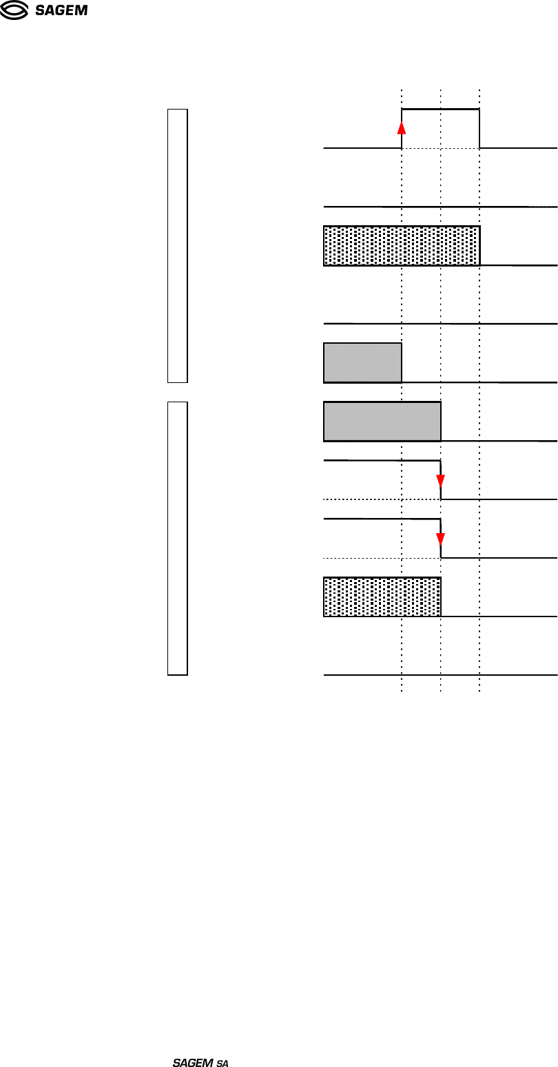
Ref : SCT TMO MOD SPEC 662
Rev.: B
Ref. sec. :
Date: 18/11/2004
Document . All rights of reproduction and disclosure reserved.
MO2XX module – Confidential under NDA Page 60/67
MOD_ON_CMD
MOD_OFF_CMD
DTE_UART_STATE
MOD_RESET_CMD
MOD_UART_STATE
MOD_ON_STATE
MOD_FLOW_STATE
RX
TX
D
C
E
i
n
p
u
t
s
D
C
E
o
u
t
p
u
t
s
MOD_RESET_STATE
Another solution to switch off the MO2XX is the AT command AT+CPOF:
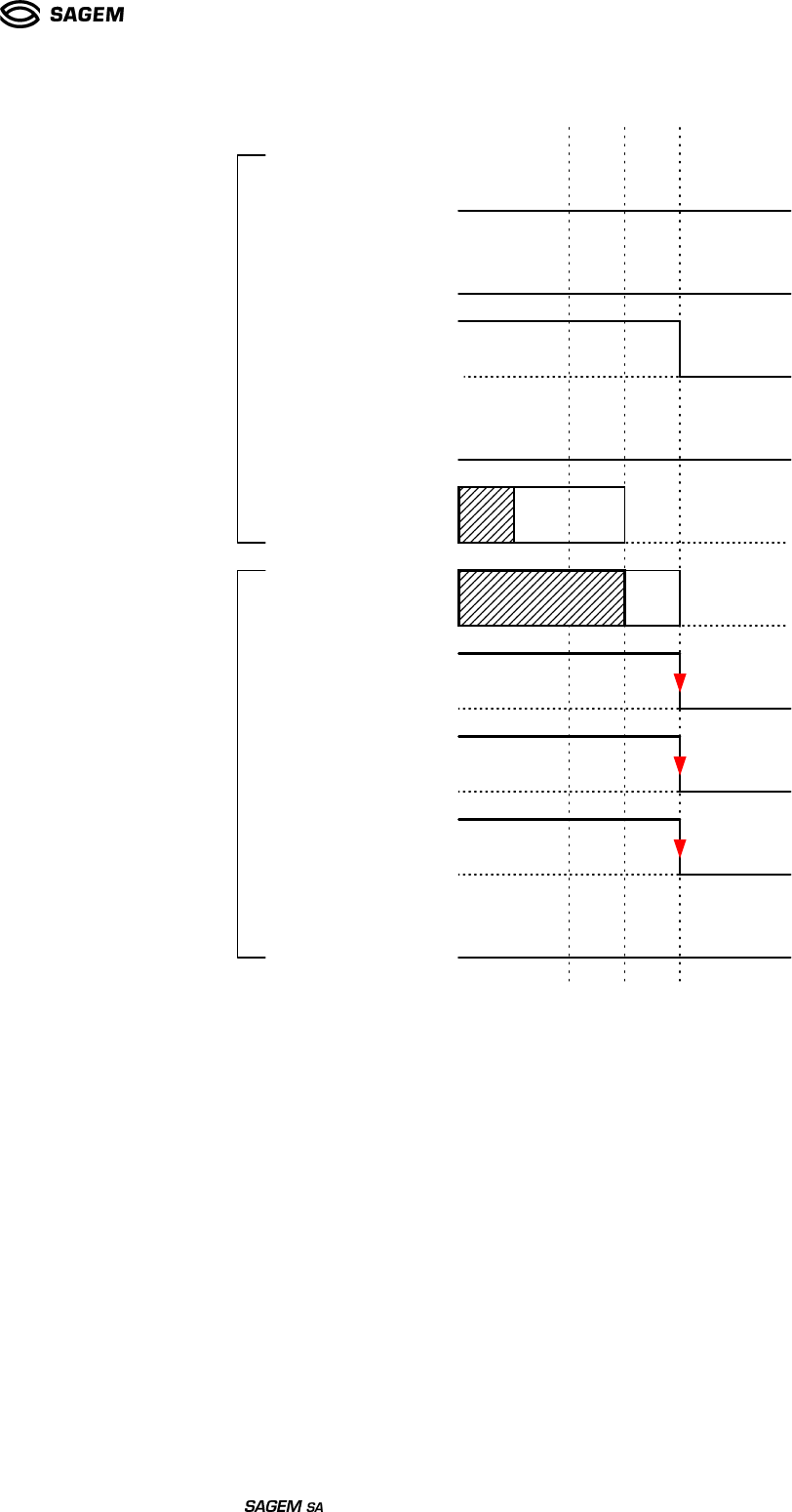
Ref : SCT TMO MOD SPEC 662
Rev.: B
Ref. sec. :
Date: 18/11/2004
Document . All rights of reproduction and disclosure reserved.
MO2XX module – Confidential under NDA Page 61/67
MOD_ON_CMD
MOD_OFF_CMD
DTE_UART_STATE
MOD_RESET_CMD
MOD_UART_STATE
MOD_ON_STATE
MOD_FLOW_STATE
RX
TX
D
C
E
i
n
p
u
t
s
D
C
E
o
u
t
p
u
t
s
MOD_RESET_STATE
AT+CPOF
OK
1.3.3.8. Reset
There are 2 possibilities :
• The MO2XX reboots by itself for a major internal problem and warns the DTE of this operation. In
this case, the MO2XX moves the MOD_RESET_STATE signal to Active. At the end of the reset
operation, the MO2XX deactivate this signal and its current state is ON Active.
• The DTE orders the MO2XX to reset. In this case, the DTE moves the MOD_RESET_CMD signal
to initiate the process.
The latest data sent by the DTE should be considered as lost and resent to the MO2XX if need be.
This transition is possible whatever the states of the DCE and the DTE.
At the end of the RESET, the DTE and the DCE are always ON.
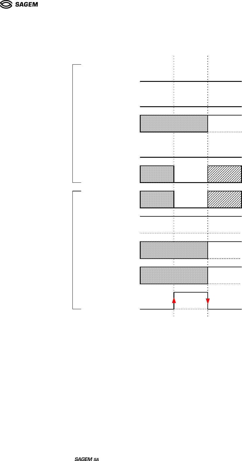
Ref : SCT TMO MOD SPEC 662
Rev.: B
Ref. sec. :
Date: 18/11/2004
Document . All rights of reproduction and disclosure reserved.
MO2XX module – Confidential under NDA Page 62/67
1.3.3.8.1. Initiated by the DCE.
MOD_ON_CMD
MOD_OFF_CMD
DTE_UART_STATE
MOD_RESET_CMD
ON
RESET
MOD_UART_STATE
MOD_ON_STATE
MOD_FLOW_STATE
RX
TX
D
C
E
o
u
t
p
u
t
s
D
C
E
i
n
p
u
t
s
MOD_RESET_STATE
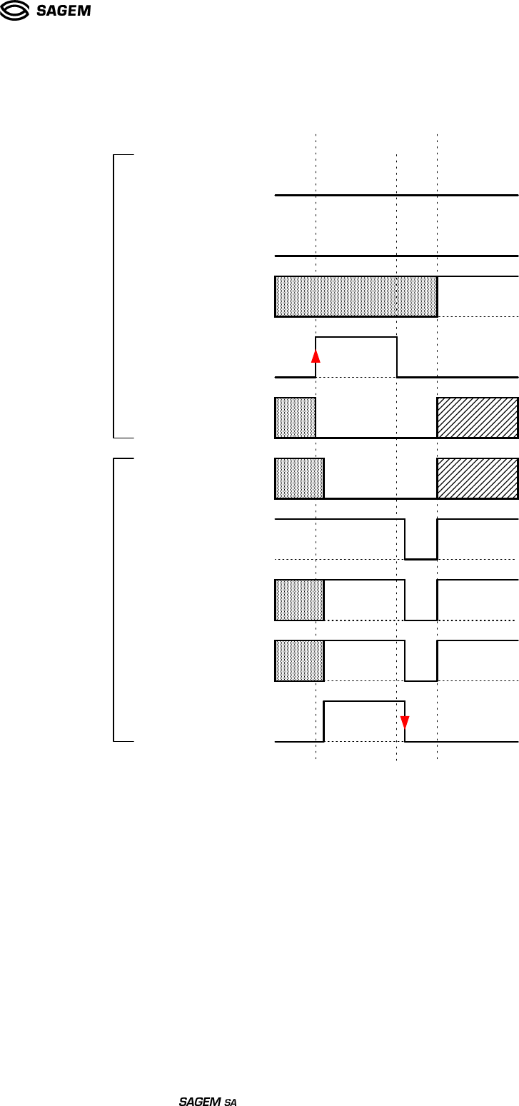
Ref : SCT TMO MOD SPEC 662
Rev.: B
Ref. sec. :
Date: 18/11/2004
Document . All rights of reproduction and disclosure reserved.
MO2XX module – Confidential under NDA Page 63/67
1.3.3.8.2. Initiated by the DTE.
MOD_ON_CMD
MOD_OFF_CMD
DTE_UART_STATE
MOD_RESET_CMD
ON
RESET
MOD_UART_STATE
MOD_ON_STATE
MOD_RESET_STATE
RX
TX
D
C
E
o
u
t
p
u
t
s
D
C
E
i
n
p
u
t
s
MOD_FLOW_STATE
1.3.3.9. Timeout.
If a command has no effect on the other equipment, it must be requested again after a one second
timeout. The maximum number of requests is 5 and then a reset procedure of the DCE must be
initiated by the DTE.
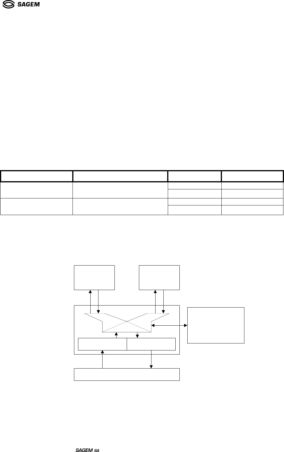
Ref : SCT TMO MOD SPEC 662
Rev.: B
Ref. sec. :
Date: 18/11/2004
Document . All rights of reproduction and disclosure reserved.
MO2XX module – Confidential under NDA Page 64/67
ANNEX 3 : Data/Command hardware multiplexing
1. Hardware multiplexing
1.1. External interfaces
In the first set (hardware MUX), we need to use two hardware signals (MOD_ESCAPE*_CMD and
DTE_ESCAPE_CMD) and the full serial link V24.
In the second set, we only need to use the full V24.
To make an interface with a host, the MO2xx hardware multiplexing signals need no added hardware.
1.2. Capability requirements
1.2.1. Logical and electrical levels
Signal Logical levels Electrical levels
Active High level
MO2xx output DTE_ESCAPE_CMD Inactive Low level
Active Low level
MO2xx input MOD_ESCAPE*_CMD Inactive High level
1.2.2. Hardware protocol
SET_2 :
We switch between DATA and
COMMAND
MUX
V24
reception
emission
COMMAND
DATA
Hardware management:
DTE_ESCAPE_CMD and
MOD_ESCAPE_CMD
Software management:
Escape strings detection
In the paragraphs below only the logical signals are considered
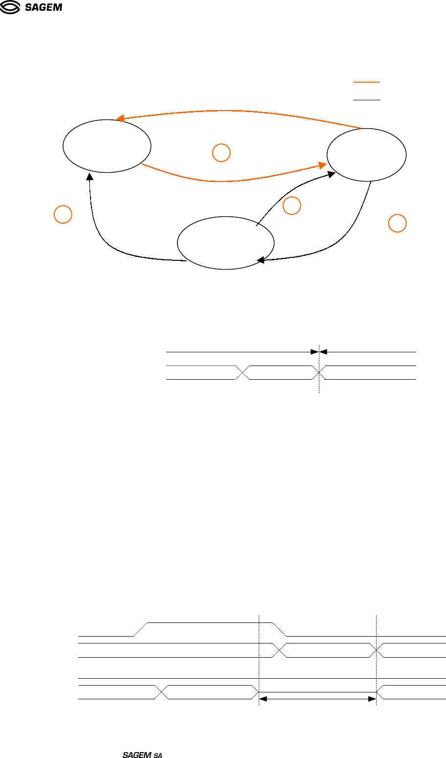
Ref : SCT TMO MOD SPEC 662
Rev.: B
Ref. sec. :
Date: 18/11/2004
Document . All rights of reproduction and disclosure reserved.
MO2XX module – Confidential under NDA Page 65/67
1.2.3. State diagram
1.2.4. Transition (1): Command -> Data
The data connection is established when the PDA receives the “CONNECT: <speed>” message
from the SB.
CONNECT:9600
Modem Tx
Command mode
Data mode
Remark:
The Connect message is different between voice call, a classical data connection, a GPRS data connection
and a fax call, so it is necessary to treat the entire message to separate the data and voice calls.
1.2.5. Transition (2): Data -> Suspended Data
The modem or the DTE can request this transition, so it is necessary to distinguish two cases.
1st case: the DTE orders the modem to go in the suspended data mode
1. The DTE indicates the order by moving MOD_ESCAPE*_CMD and then begins to search in the data flow the
MOD_ESCAPE_STR from the modem.
2. When the modem is ready, it sends the MOD_ESCAPE_STR string and it wait for DTE_ESCAPE_STR.
3. When receiving this string, the DTE then move back MOD_ESCAPE*_CMD and sends the
DTE_ESCAPE_STR, which indicates to the modem every byte after that must be considered as part as an AT
Command
Modem Tx
DTE_ESCAPE_CMD
DTE Tx
MOD_ESCAPE_CMD
MOD_ESCAPE_STR
DATA
COMMAND
DATA
DTE_ESCAPE_STR
COMMAND
Wait for
DTE_ESCAPE_STR
DTE : MOD_ESCAPE*_CMD
OR
Modem : DTE_ESCAPE_CMD
Already implemented
COMMAND
DATA
SUSPENDED
DATA
DTE : +++
DTE : ATO
DTE : ATO
DTE : ATH
OU
Modem : NO CARRIER
To be defined
2
4
3
1
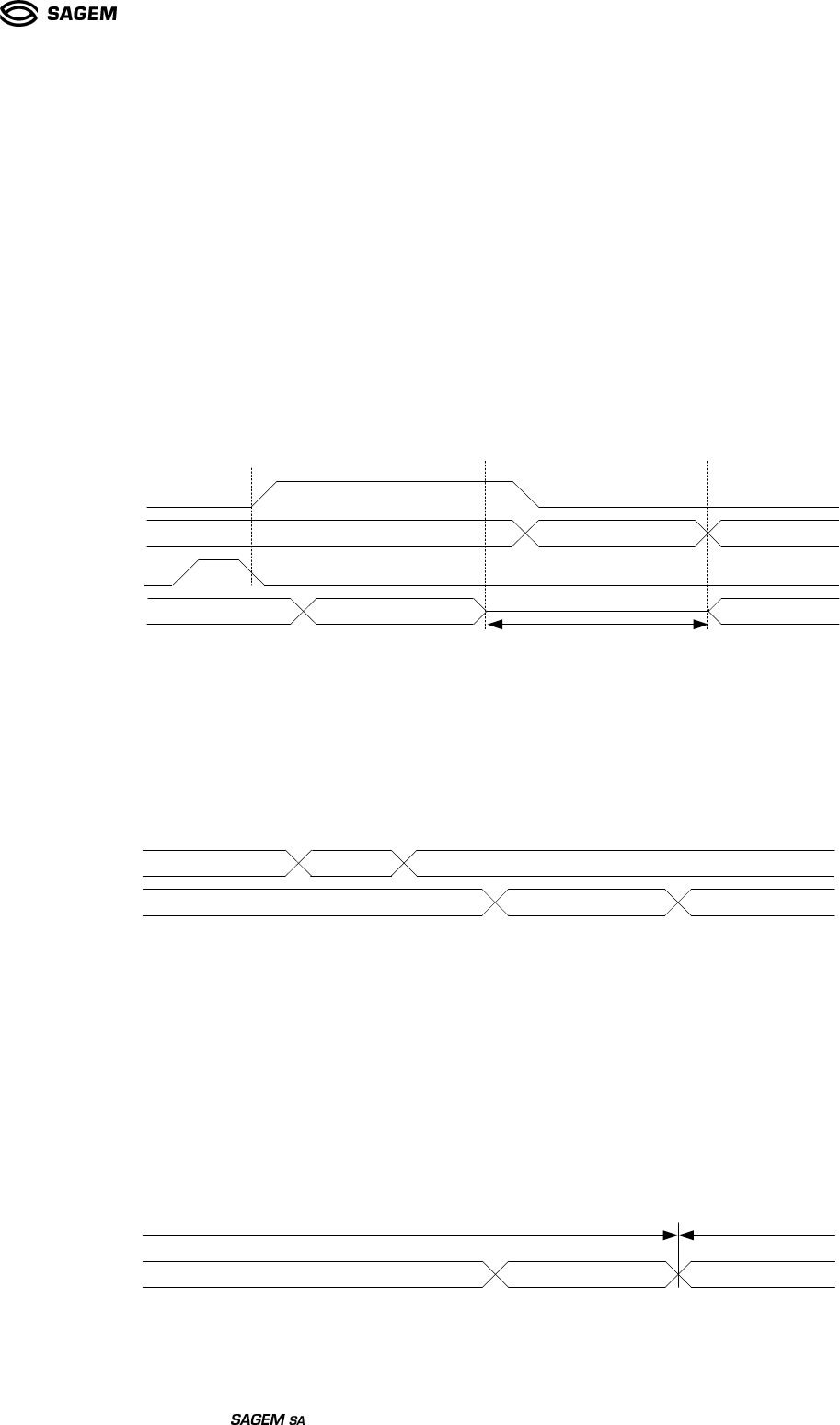
Ref : SCT TMO MOD SPEC 662
Rev.: B
Ref. sec. :
Date: 18/11/2004
Document . All rights of reproduction and disclosure reserved.
MO2XX module – Confidential under NDA Page 66/67
Remarks:
• DTE_ESCAPE_CMD = MOD_ESCAPE_CMD = {0x18,0x7E,0xDB,0xFF}, this string could be change by
AT command in the future.
• These two strings are the effective separation between the data flow and the command flow
2nd case: the modem requests the DTE to go in the suspended data mode
1. The modem indicates the request by moving DTE_ESCAPE_CMD.
2. The DTE indicates the order by moving MOD_ESCAPE*_CMD and then begins to search in the data flow the
MOD_ESCAPE_STR from the modem.
3. When the modem is ready, it sends the MOD_ESCAPE_STR string and it wait for DTE_ESCAPE_STR.
4. When receiving this string, the DTE then move back MOD_ESCAPE*_CMD and sends the
DTE_ESCAPE_STR, which indicates to the modem every byte after that must be considered as part as an AT
Command
Modem Tx
DTE_ESCAPE_CMD
DTE Tx
MOD_ESCAPE_CMD
MOD_ESCAPE_STR
DATA
DATA
DTE_ESCAPE_STR
COMMAND
COMMAND
Wait for
DTE_ESCAPE_STR
1.2.6. Transition (3): Suspended Data -> Data Mode
This transition is always ordered by the PDA via the classical ATO command.
The SB acknowledges with the CONNECT message
Modem Tx
DTE Tx
DATA
COMMAND
ATO
DATA
COMMAND
CONNECT:9600
1.2.7. Transition (4): Suspended Data -> Command Mode
The theoretical transition is Data to Command and happens to end a data connection; the
Suspended Data Mode is just a temporary transition between the two.
The real procedure is Data to Suspended Data (already detailed in transition 2) and then Suspended Data
to Command Mode.
There are two different cases:
• Or the distant can hang up and then the modem is going to send a “NO CARRIER” message
Modem Tx
COMMAND
NO CARRIER
COMMAND
Suspended data mode
Command mode
• Or the DTE wants to hang up and then an ATH is sent and the transition has to be made on the answer
to this command (OK)
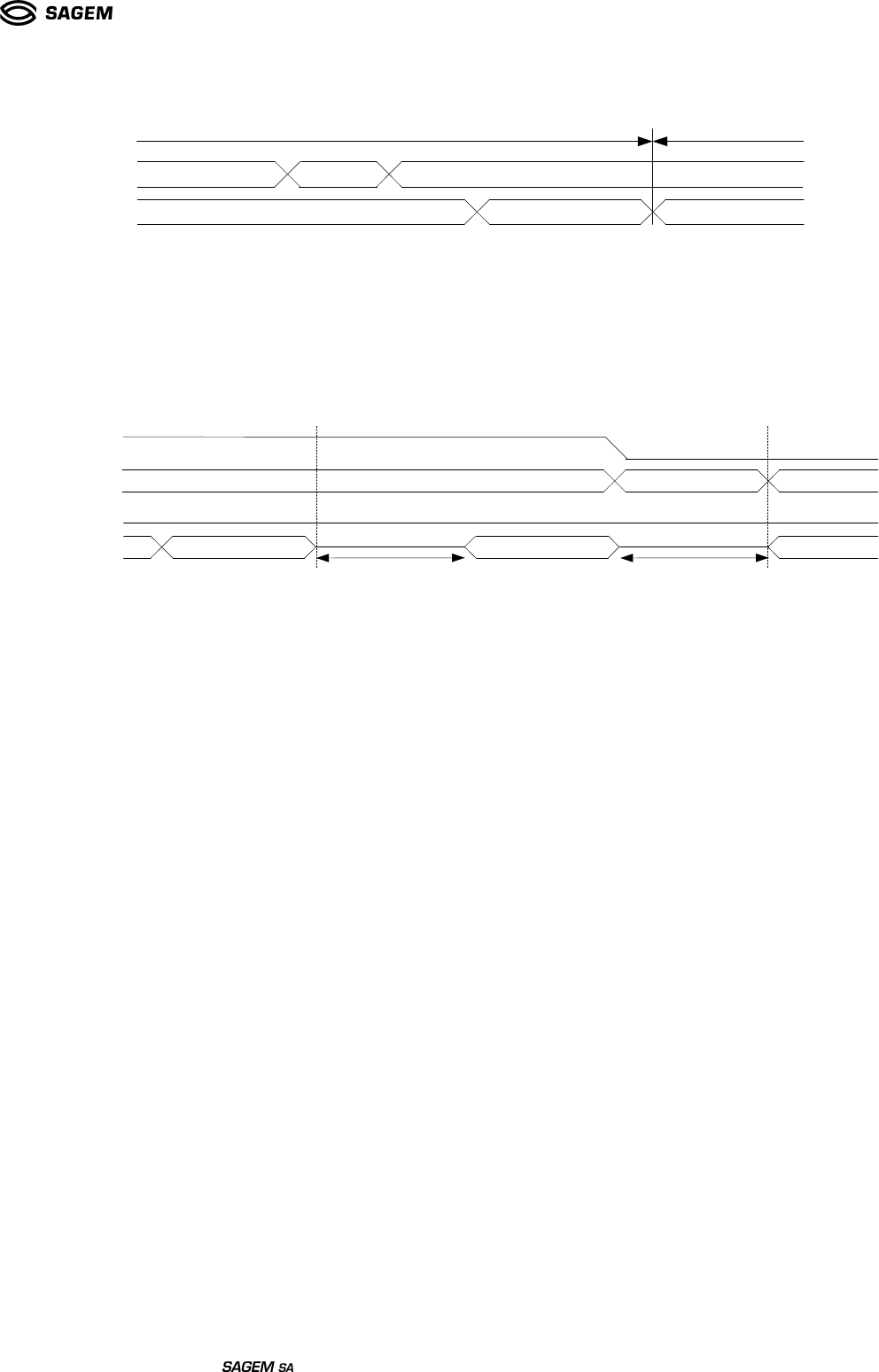
Ref : SCT TMO MOD SPEC 662
Rev.: B
Ref. sec. :
Date: 18/11/2004
Document . All rights of reproduction and disclosure reserved.
MO2XX module – Confidential under NDA Page 67/67
Modem Tx
DTE Tx
COMMAND
COMMAND
ATH
COMMAND
COMMAND
OK
Suspended data mode
Command mode
1.2.8. Timeout case
If modem didn’t receive the DTE_ESCAPE_STR after a timeout (2s), it send again his
MOD_ESCAPE_STR and wait for DTE_ESCAPE_STR as long as the MOD_ESCAPE*_CMD signal
is active. After 3 retry, module closes the MUX mechanism.
Modem Tx
DTE_ESCAPE_CMD
DTE Tx
MOD_ESCAPE_CMD
MOD_ESCAPE_STR
DATA
COMMAND
DATA
DTE_ESCAPE_STR
COMMAND
Time out
MOD_ESCAPE_STR
Wait for
DTE_ESCAPE_STR
Remarks:
If MOD_ESCAPE_CMD returns in inactive mode and the escape string hasn’t been received by the
modem, we have to resume the data connection.
---
END OF DOCUMENT
---