Samsung Electronics Co SIP0P5WRS50 ARTIK055s User Manual Samsung ARTIK ation
Samsung Electronics Co Ltd ARTIK055s Samsung ARTIK ation
User Manual
SIP0P5WRS50
Samsung Semiconductor, Inc. SIP0P5WRS50 Module Datasheet
Samsung Confidential
Specifications in this document are tentative and subject to change.
2
Samsung’s ARTIK™ Module is a highly integrated module for
secure Internet of Things (IoT) devices that require Wi-Fi. It is
based on an ARM® Cortex® R4 core with on-chip memories,
an ARM® Cortex® M0+ core, a complete 2.4GHz Wi-Fi Phy,
MAC layer processing, a large complement of standard digital
buses including audio (I2S), and power management. The
module is packaged with additional external Flash memory, a
hardware Secure Element and a single integrated 2.4GHz
structural antenna.
The application processor is fully available for applications
since the Wi-Fi stack, through the MAC layer, is handled by a
co-processor. Aimed especially at power-sensitive devices
needing Wi-Fi, the SIP0P5WRS50 Module provides excellent
performance in a variety of environments, with a feature set
tailored specifically for IoT end nodes.
Top View (Image is preliminary and will change)
SIP0P5WRS50 Module Block Diagram
Processor
CPU
ARM® Cortex® R4, 32-bit
with 32KB I-Cache and
32KB D-Cache @ 320MHz
WLAN CPU
ARM Cortex M0+ @
320MHz
Memory
Embedded ROM
64KB
User Embedded RAM
1.25MB
128KB (Shared)
FLASH
8MB SPI FLASH on Module
Security
Secure Element
Secure point to point
authentication and data
transfer
Radio
WLAN
IEEE802.11™ b/g/n
2.4GHz radio
Power Management
Single Supply
Provides all power of the
SIP0P5WRS50 Module
using 3.3V
Interfaces
Digital I/O
UART, I2C, I2S, SPI, PWM
and GPIO
SAMSUNG ELECTRONICS RESERVES THE RIGHT TO CHANGE PRODUCTS, INFORMATION AND SPECIFICATIONS WITHOUT NOTICE.
Products and specifications discussed herein are for reference purposes only. All information discussed herein is provided on an "AS IS" basis, without warranties
of any kind. This document and all information discussed herein remain the sole and exclusive property of Samsung Electronics. No license of any patent,
copyright, mask work, trademark or any other intellectual property right is granted by one party to the other party under this document, by implication, estoppel
or other-wise. Samsung products are not intended for use in life support, critical care, medical, safety equipment, or similar applications where product failure
could result in loss of life or personal or physical harm, or any military or defense application, or any governmental procurement to which special terms or
provisions may apply. For updates or additional information about Samsung products, contact your nearest Samsung office. All brand names, trademarks and
registered trademarks belong to their respective owners.
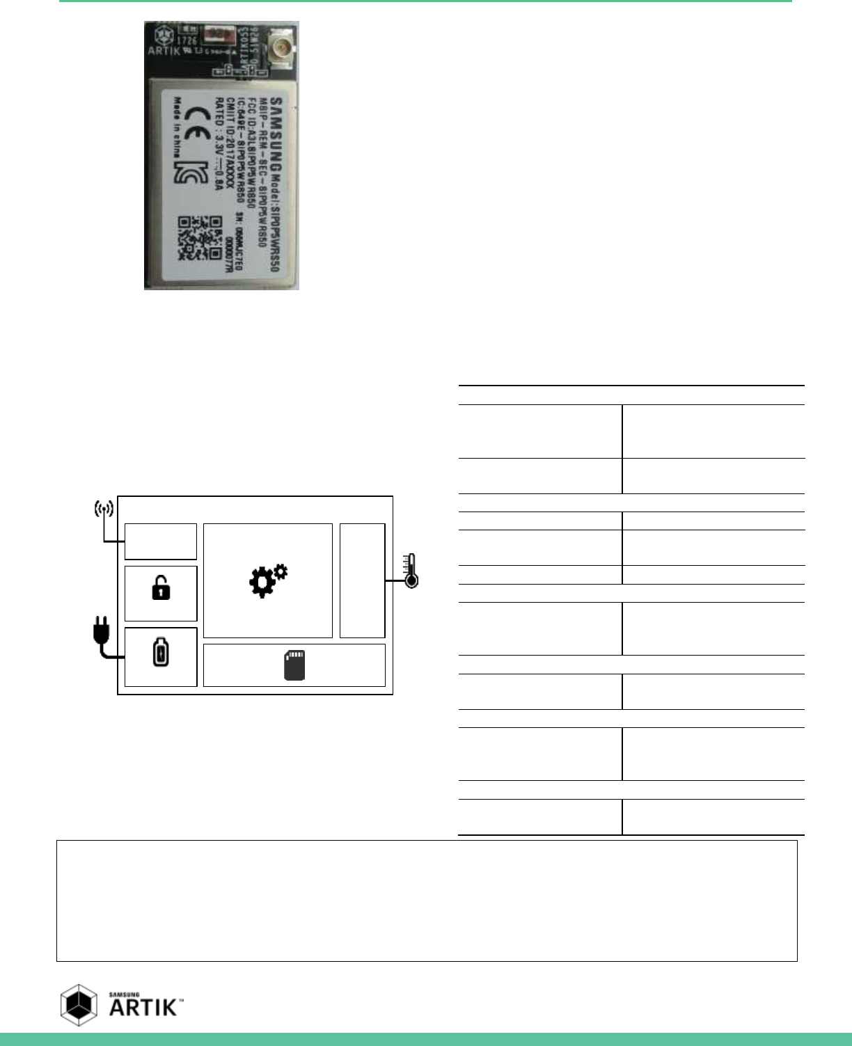
ARTIK 051 MODULE
RADIO
SECURITY
PROCESSOR
POWER MGT. MEMORY
INTERFACES

Samsung Semiconductor, Inc. SIP0P5WRS50 Module Datasheet
Samsung Confidential
Specifications in this document are tentative and subject to change.
3
TABLE OF CONTENTS
Table of Contents ................................................................................................................................................................... 3
List of Figures .......................................................................................................................................................................... 4
List of Tables ........................................................................................................................................................................... 4
Version History ...................................................................................................................................................................................... 5
SIP0P5WRS50 Module Block Diagram and Component Placement ................................................................................ 6
SIP0P5WRS50 Module Wi-Fi Interface ................................................................................................................................................ 6
SIP0P5WRS50 Module Memory ........................................................................................................................................................... 6
SIP0P5WRS50 Module Power Management Unit .............................................................................................................................. 7
SIP0P5WRS50 Module Security Subsystem ........................................................................................................................................ 7
SIP0P5WRS50 Module ADC Interface .................................................................................................................................................. 7
SIP0P5WRS50 Module UART Interface ................................................................................................................................................ 8
SIP0P5WRS50 Module GPIO Interface ................................................................................................................................................ 8
SIP0P5WRS50 INT Interface ................................................................................................................................................................. 8
SIP0P5WRS50 Module I2C Interface .................................................................................................................................................... 9
SIP0P5WRS50 Module SPI Interface.................................................................................................................................................... 9
SIP0P5WRS50 Module PWM Interface ................................................................................................................................................ 9
SIP0P5WRS50 Module I2S Interface .................................................................................................................................................... 9
SIP0P5WRS50 Module Processor System ........................................................................................................................................... 9
SIP0P5WRS50 Module Edge Connector ............................................................................................................................ 10
SIP0P5WRS50 Functional Interfaces .................................................................................................................................. 13
ADC Interface ....................................................................................................................................................................................... 13
Debug Interface ................................................................................................................................................................................... 13
GPIO Interface ..................................................................................................................................................................................... 13
I2C Interface ......................................................................................................................................................................................... 14
INT Interface ........................................................................................................................................................................................ 14
Power Interface ................................................................................................................................................................................... 14
PWM Interface ..................................................................................................................................................................................... 14
Reset Interface ..................................................................................................................................................................................... 15
SPI Interface ........................................................................................................................................................................................ 15
UART Interface ..................................................................................................................................................................................... 15
SIP0P5WRS50 Module GPIO Alternate Functions ............................................................................................................ 16
SIP0P5WRS50 Module Booting Sequence......................................................................................................................... 18
SIP0P5WRS50 Module Wi-Fi Antenna structure ............................................................................................................... 19
SIP0P5WRS50 Module Electrical Specifications ................................................................................................................ 19
Absolute Maximum Rating ................................................................................................................................................................. 20
DC Electrical Characteristics .............................................................................................................................................................. 20
DC Module Use Case Characteristics ................................................................................................................................................ 21
Power Supply Requirements .............................................................................................................................................................. 21
ESD Ratings .......................................................................................................................................................................................... 21
RF Electrical Characteristics ............................................................................................................................................................... 21
SIP0P5WRS50 Module Mechanical Specifications ........................................................................................................... 22
SIP0P5WRS50 Module FCC Certification ........................................................................................................................... 23
SIP0P5WRS50 Module Ordering Information ................................................................................................................... 24
Legal Information ................................................................................................................................................................. 25

Samsung Semiconductor, Inc. SIP0P5WRS50 Module Datasheet
Samsung Confidential
Specifications in this document are tentative and subject to change.
4
LIST OF FIGURES
Figure 1. SIP0P5WRS50 Module Block Diagram ................................................................................................................... 6
Figure 2. ADC LSB behavior .................................................................................................................................................... 8
Figure 3. SIP0P5WRS50 Module Edge Connector ............................................................................................................. 10
Figure 4. Booting and Reset Timing Relations ................................................................................................................... 18
Figure 5. RF Connector for Wi-Fi Antenna ............................................................ 오류! 책갈피가 정의되어 있지 않습니다.
Figure 6. SIP0P5WRS50 Module Mechanical Dimensions ................................................................................................ 22
LIST OF TABLES
Table 1. SIP0P5WRS50 Module Edge Connector Table Signal Descriptions .................................................................. 10
Table 2. ADC Interface .......................................................................................................................................................... 13
Table 3. Debug Interface ...................................................................................................................................................... 13
Table 4. GPIO Interface ......................................................................................................................................................... 13
Table 5. I2C Interface ............................................................................................................................................................. 14
Table 6. Interrupt Interface .................................................................................................................................................. 14
Table 7. PWM Interface......................................................................................................................................................... 14
Table 8. Reset Interface ........................................................................................................................................................ 15
Table 9. SPI Interface ............................................................................................................................................................ 15
Table 10. UART Interface ...................................................................................................................................................... 15
Table 11. Alternate functions of the SIP0P5WRS50 Module............................................................................................ 16
Table 12. Absolute Maximum Ratings ................................................................................................................................ 20
Table 13. I/O DC Electrical Characteristics(PAD:5,6,14-26,29-31,33-42,44-73, IO) ........................................................ 20
Table 14. I/O DC Electrical Characteristics(PAD:2-5, ADC) ............................................................................................... 20
Table 15. Recommended Operating Conditions ............................................................................................................... 21
Table 16. I/O Drive Strength ................................................................................................................................................ 21
Table 17. ESD Ratings ........................................................................................................................................................... 21
Samsung Semiconductor, Inc. SIP0P5WRS50 Module Datasheet
Samsung Confidential
Specifications in this document are tentative and subject to change.
5
VERSION HISTORY
Revision
Date
Description
Maturity
V0.1
07/26/2017
First Draft SIP0P5WRS50 Module Datasheet
Pre Alpha
V0.11
8/24/2017
Add legal information
Pre Alpha
V0.12
8/30/2017
Fix typos
Pre Alpha
Samsung Semiconductor, Inc. SIP0P5WRS50 Module Datasheet
Samsung Confidential
Specifications in this document are tentative and subject to change.
6
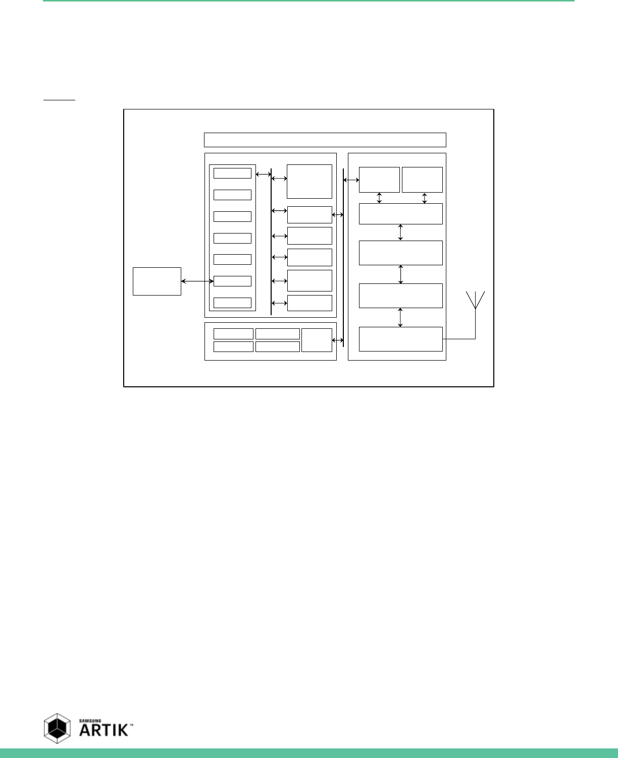
SIP0P5WRS50 MODULE BLOCK DIAGRAM AND
COMPONENT PLACEMENT
Figure 1 shows the functional Block Diagram of the SIP0P5WRS50 Module.
Figure 1. SIP0P5WRS50 Module Block Diagram
SIP0P5WRS50 MODULE WI-FI INTERFACE
The SIP0P5WRS50 Module has an 802.11b/g/n Wi-Fi subsystem. The most important hardware features of the Wi-Fi system
are:
802.11b/g/n support @ 2.4GHz
20MHz SISO (802.11n)
UDP throughput up to 50Mbps
WPA/WPA2/WAPI with WEP/TKIP implemented in software
Dedicated Wi-Fi Processor Sub System
o ARM® Cortex® R4 Processor @ 480 MHz
o Operating frequency of 320MHz
o 32KB I-Cache
o 16KB D-Cache
o Tightly Coupled Memory (32KB Code Memory/32KB Data Memory)
o SRAM 96KB
SIP0P5WRS50 MODULE MEMORY
The SIP0P5WRS50 Module has a memory subsystem with the following hardware features:
Internal RAM for secure boot, secure OS and general purpose operations.
o 1280KB dedicated RAM
User Domain
UART
PWM
SPI
GPIO
DEBUG
I2S
PROCESSOR
CORTEX R4
32KB I$
32KB D$
BRIDGE
CRYPTO
ACCELERATOR
DMA
TCM
RAM/ ROM
32KB/ 32KB
BRIDGE
WLAN CO-PROCESSOR
32KB I-Cache, 16KB D-Cache
96KB SRAM
80 2.11 MAC
WLAN DOMAIN
2.4GHz
RADIO
RTC
PMU
PLL
LDO BRIDGE
80 2.11 PHY
I2C
1.25MB SRAM
128KB SRAM
64KB ROM
UART <-> USB
PMIC

Samsung Semiconductor, Inc. SIP0P5WRS50 Module Datasheet
Samsung Confidential
Specifications in this document are tentative and subject to change.
7
o 128KB shared RAM
Internal ROM for secure boot and secure OS operations.
o 64KB dedicated ROM
SIP0P5WRS50 MODULE POWER MANAGEMENT UNIT
The SIP0P5WRS50 Module has one universal power management unit that controls the state of power on the SIP0P5WRS50
Module. The most important features of the PMU are:
Fine granular power control
o Through the use of power domains
System level power control
o Deep stop mode
o Sleep power mode
Power savings techniques
o Frequency scaling
o Clock gating
o Power gating
SIP0P5WRS50 MODULE SECURITY SUBSYSTEM
The SIP0P5WRS50 Module has a dedicated security subsystem to ensure a secure end to end operation in any IoT
environment. The most important features of the SIP0P5WRS50 Module security subsystem are:
Isolated Execution Environment
o Isolated Cortex-M0 processor
o 8KB ROM for secure booting
o 32KB secure SRAM
o Dedicated secure DMA channel for secure backup/restore of SRAM content
o Secure Mailbox (68x32b wide) for secure communication
o Isolated key support
Backup encryption key 256-bits
SSS root private key 521-bits
Storage key 256-bits
Symmetric key engines
o Secure AES
o Secure DES/Triple-DES
Stream cipher engine
o ARC4 engine
Various Hash engines
o SHA-1/SHA2-256/ SHA2-384/ SHA2-512/MD5 HMAC
Asymmetric key engines
o PKA (Public Key Accelerator) engine
PRNG (Pseudo Random Number Generator)
DTRNG (Digital True RNG)
Secure timer
Secure key manager
DMA Support, Descriptor DMA
Block ciphers + hashing
Retention reset scheme
SIP0P5WRS50 MODULE ADC INTERFACE
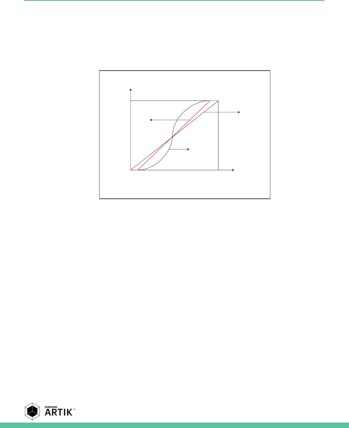
The SIP0P5WRS50 Module has one 4-channel selectable analog to digital converter. The most important hardware features of
the A/D interface are:
Programmable 4-channel selection
Samsung Semiconductor, Inc. SIP0P5WRS50 Module Datasheet
Samsung Confidential
Specifications in this document are tentative and subject to change.
8
Main ADC clock at 6.5MHz
Conversion clock ADC at 1.08MHz
Support for selectable conversion mode: 1, 2, 4, 8, 16, 32, 64
Differential non-linearity error ±2 LSB
Integral non-linearity error ±6 LSB
Top offset error ±10 LSB
Bottom offset error ±10 LSB
Figure 2 depicts the dynamic behavior between input voltage on the ADC and resulted LSB value in the ADC register.
Figure 2. ADC LSB behavior
SIP0P5WRS50 MODULE UART INTERFACE
By default the SIP0P5WRS50 Module has three, 2-pin UART interfaces. Using GPIOs that are currently used for other
functionality you can potentially create two 4-pin UART interfaces. The most important hardware features of the UART
interface is:
The UART can be operated in DMA or interrupt-based mode
Support for 5-bit, 6-bit, 7-bit or 8-bit serial data transmit and receive
Programmable baud rate
One or two stop bit insertion
SIP0P5WRS50 MODULE GPIO INTERFACE
The SIP0P5WRS50 Module has an extensive general purpose Input/Output interface. The most important features of the
SIP0P5WRS50 Module GPIO interface are:
Support for 62 multi-function input output ports.
Support for 27 dedicated GPIO ports
Control of 16 external interrupts
SIP0P5WRS50 INT INTERFACE
The SIP0P5WRS50 Module is equipped with an interrupt controller. The most important features of the SIP0P5WRS50 Module
Interrupt Interface are:
Enable, disable and generate interrupts from peripheral sources
Software generated interrupts
Interrupt masking and prioritization
Result (LSB)
Analog in (V)
Top
offset
Bottom
offset
Real
value
Ideal
value
Ideal value
with offset

Samsung Semiconductor, Inc. SIP0P5WRS50 Module Datasheet
Samsung Confidential
Specifications in this document are tentative and subject to change.
9
Wake-up events for power management
Control of 3 external wakeup interrupts
SIP0P5WRS50 MODULE I2C INTERFACE
By default the SIP0P5WRS50 Module has two high speed multi-master I2C interfaces available with speeds up to 3.4Mbps.
Using GPIOs that are currently used for other functionality you can potentially create four I2C interfaces.
SIP0P5WRS50 MODULE SPI INTERFACE
By default the SIP0P5WRS50 Module has two dedicated SPI interfaces. Using GPIOs that are currently used for other
functionality you can potentially create four SPI interfaces. The most important hardware features of the SPI interfaces are:
Full duplex communication
8, 16 or 32-bit shift registers and bus interface
Motorola SPI protocol and National Semiconductor Microwire protocol
Master and slave mode operation
Two independent 32-bit wide transmit/receive FIFOs
Transmit and receive speeds up to 50MHz
SIP0P5WRS50 MODULE PWM INTERFACE
By default the SIP0P5WRS50 Module has seven PWM timers available. The most important features of the PWM interfaces
are:
32-bit size timers on each PWM signal
Two 8-bit pre-scalers (first level of division) and 5 clock-dividers/multiplexers for second level division
Static configuration option
Dynamic configuration option
Auto-reload and One-shot pulse mode
Dead zone generator
Level interrupt generation
SIP0P5WRS50 MODULE I2S INTERFACE
By default the SIP0P5WRS50 Module does not have an I2S interface, however when re-using the right GPIO pins one I2S
interface can be allocated. The most important features of the I2S interface are:
Stereo channel support with external DMA based operation
Mixes up to two sound sources
Support for serial data transfer of 8, 16 or 32-bit per channel
Support for slave mode
SIP0P5WRS50 MODULE PROCESSOR SYSTEM
The ARTIK 51 Module has one dedicated Cortex®-R4 processor dedicated towards application processing. The main features
of the main processor are:
Cortex® R4 ARM® processor
CPU speed 320MHz
32kB Instruction cache
32kB Data cache
Samsung Semiconductor, Inc. SIP0P5WRS50 Module Datasheet
Samsung Confidential
Specifications in this document are tentative and subject to change.
10
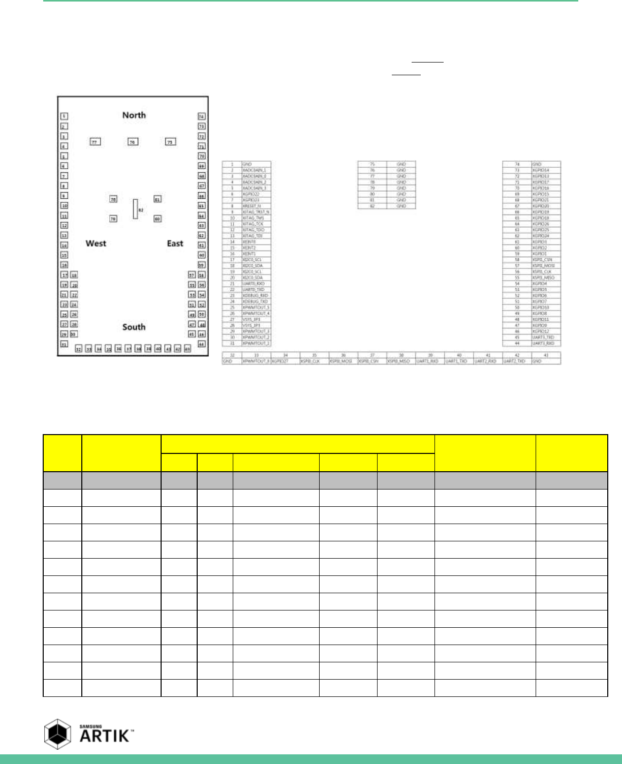
SIP0P5WRS50 MODULE EDGE CONNECTOR
The SIP0P5WRS50 Module utilizes 74 signals and ground pins providing all the relevant signaling. Figure 3 shows how the Edge Connector is
oriented and how signal-coordinates are assigned to the edge of the SIP0P5WRS50 Module. Table 1 describes the relation between the edge
coordinates and the signal names.
Figure 3. SIP0P5WRS50 Module PAD map
Table 1. SIP0P5WRS50 Module Edge Connector Table Signal Descriptions
Pin
No.
Pin Name
GPIO
Function1
Function2
I/O
PUD
POWER
Grp
GPIO
1
GND
2
XADC0AIN_1
-
-
AVDD18_ADC0
ADC
3
XADC0AIN_0
-
-
AVDD18_ADC0
ADC
4
XADC0AIN_2
-
-
AVDD18_ADC0
ADC
5
XADC0AIN_3
-
-
AVDD18_ADC0
ADC
6
XGPIO22
I
PD
VDDQ1833_SDIO_0
GPG2
GPG2[6]
GPIO
7
XGPIO23
I
PD
VDDQ1833_SDIO_0
GPG2
GPG2[7]
GPIO
8
XRESET_N
I
-
VDDQ33_EXT1
System Reset
9
XJTAG_TRST_N
I
PD
VDDQ33_EXT1
ETC0
ETC0[0]
JTAG
10
XJTAG_TMS
I
PU
VDDQ33_EXT1
ETC0
ETC0[1]
JTAG
11
XJTAG_TCK
I
PD
VDDQ33_EXT1
ETC0
ETC0[2]
JTAG
12
XJTAG_TDO
I
PD
VDDQ33_EXT1
ETC0
ETC0[4]
JTAG
13
XJTAG_TDI
I
PU
VDDQ33_EXT1
ETC0
ETC0[3]
JTAG
Samsung Semiconductor, Inc. SIP0P5WRS50 Module Datasheet
Samsung Confidential
Specifications in this document are tentative and subject to change.
11
14
XEINT0
I
PD
VDDQ33_EXT1
GPA0
GPA0[0]
External Interrupt
15
XEINT2
I
PD
VDDQ33_EXT1
GPA0
GPA0[2]
External Interrupt
16
XEINT1
I
PD
VDDQ33_EXT1
GPA0
GPA0[1]
External Interrupt
17
XI2C0_SCL
I
PD
VDDQ33_EXT1
GPA1
GPA1[0]
HSI2C_0_SCL
18
XI2C0_SDA
I
PD
VDDQ33_EXT1
GPA1
GPA1[1]
HSI2C_0_SDA
19
XI2C1_SCL
I
PD
VDDQ33_EXT1
GPA1
GPA1[2]
HSI2C_1_SCL
20
XI2C1_SDA
I
PD
VDDQ33_EXT1
GPA1
GPA1[3]
HSI2C_1_SDA
21
XUART0_RXD
I
PD
VDDQ33_EXT1
GPA2
GPA2[0]
UART0_RXD
22
XUART0_TXD
I
PD
VDDQ33_EXT1
GPA2
GPA2[1]
UART0_TXD
23
XDEBUG_RXD
I
PD
VDDQ33_EXT1
GPA3
GPA3[0]
XDEBUG_RXD
24
XDEBUG_TXD
I
PD
VDDQ33_EXT1
GPA3
GPA3[1]
XDEBUG_TXD
25
XPWMTOUT_5
I
PD
VDDQ33_EXT0
GPP2
GPP2[6]
PWMTOUT_5
26
XPWMTOUT_4
I
PD
VDDQ33_EXT0
GPP2
GPP2[5]
PWMTOUT_4
27
3V3_EXT_LDO2
28
3V3_EXT_LDO2
29
XPWMTOUT_3
I
PD
VDDQ33_EXT0
GPP2
GPP2[3]
PWMTOUT_3
30
XPWMTOUT_2
I
PD
VDDQ33_EXT0
GPP2
GPP2[2]
PWMTOUT_2
31
XPWMTOUT_1
I
PD
VDDQ33_EXT0
GPP2
GPP2[1]
PWMTOUT_1
UART_3_RTSn
32
GND
33
XPWMTOUT_0
I
PD
VDDQ33_EXT0
GPP2
GPP2[0]
PWMTOUT_0
UART_3_CTSn
34
XGPIO27
I
PD
VDDQ33_EXT0
GPG3
GPG3[3]
GPIO
35
XSPI0_CLK
I
PD
VDDQ33_EXT0
GPP0
GPP0[0]
SPI0_CLK
36
XSPI0_MOSI
I
PD
VDDQ33_EXT0
GPP0
GPP0[3]
SPI0_MOSI
37
XSPI0_CSN
I
PD
VDDQ33_EXT0
GPP0
GPP0[1]
SPI0_CSN
38
XSPI0_MISO
I
PD
VDDQ33_EXT0
GPP0
GPP0[2]
SPI0_MISO
39
XUART1_RXD
I
PD
VDDQ33_EXT0
GPP0
GPP0[4]
UART1_RXD
UART_2_CTSn
40
XUART1_TXD
I
PD
VDDQ33_EXT0
GPP0
GPP0[5]
UART1_TXD
UART_2_RTSn
41
XUART2_RXD
I
PD
VDDQ33_EXT0
GPP0
GPP0[6]
UART2_RXD
42
XUART2_TXD
I
PD
VDDQ33_EXT0
GPP0
GPP0[7]
UART2_TXD
43
GND
44
XUART3_RXD
I
PD
VDDQ33_EXT0
GPP1
GPP1[6]
UART3_RXD
45
XUART3_TXD
I
PD
VDDQ33_EXT0
GPP1
GPP1[7]
UART3_TXD
46
XGPIO12
I
PD
VDDQ33_EXT0
GPG1
GPG1[4]
GPIO
47
XGPIO9
I
PD
VDDQ33_EXT0
GPG1
GPG1[1]
SPI_3_CSn
48
XGPIO11
I
PD
VDDQ33_EXT0
GPG1
GPG1[3]
SPI_3_MOSI
49
XGPIO8
I
PD
VDDQ33_EXT0
GPG1
GPG1[0]
SPI_3_CLK
50
XGPIO10
I
PD
VDDQ33_EXT0
GPG1
GPG1[2]
SPI_3_MISO
51
XGPIO7
I
PD
VDDQ33_EXT0
GPG0
GPG0[7]
SPI_2_MOSI
52
XGPIO6
I
PD
VDDQ33_EXT0
GPG0
GPG0[6]
SPI_2_MISO
Samsung Semiconductor, Inc. SIP0P5WRS50 Module Datasheet
Samsung Confidential
Specifications in this document are tentative and subject to change.
12
53
XGPIO5
I
PD
VDDQ33_EXT0
GPG0
GPG0[5]
SPI_2_CSn
54
XGPIO4
I
PD
VDDQ33_EXT0
GPG0
GPG0[4]
SPI_2_CLK
55
XSPI1_MISO
I
PD
VDDQ33_EXT0
GPP4
GPP4[2]
SPI1_MISO
56
XSPI1_CLK
I
PD
VDDQ33_EXT0
GPP4
GPP4[0]
SPI1_CLK
57
XSPI1_MOSI
I
PD
VDDQ33_EXT0
GPP4
GPP4[3]
SPI1_MOSI
58
XSPI1_CSN
I
PD
VDDQ33_EXT0
GPP4
GPP4[1]
SPI1_CSN
59
XGPIO1
I
PD
VDDQ33_EXT0
GPG0
GPG0[1]
GPIO
60
XGPIO2
I
PD
VDDQ33_EXT0
GPG0
GPG0[2]
HSI2C_3_SCL
61
XGPIO3
I
PD
VDDQ33_EXT0
GPG0
GPG0[3]
HSI2C_3_SDA
62
XGPIO24
I
PD
VDDQ33_EXT0
GPG3
GPG3[0]
GPIO
63
XGPIO25
I
PD
VDDQ33_EXT0
GPG3
GPG3[1]
GPIO
64
XGPIO26
I
PD
VDDQ33_EXT0
GPG3
GPG3[2]
GPIO
65
XGPIO18
I
PD
VDDQ33_EXT0
GPG2
GPG2[2]
GPIO
66
XGPIO19
I
PD
VDDQ33_EXT0
GPG2
GPG2[3]
GPIO
67
XGPIO20
I
PD
VDDQ33_EXT0
GPG2
GPG2[4]
GPIO
68
XGPIO21
I
PD
VDDQ33_EXT0
GPG2
GPG2[5]
GPIO
69
XGPIO15
I
PD
VDDQ33_EXT0
GPG1
GPG1[7]
GPIO
70
XGPIO16
I
PD
VDDQ33_EXT0
GPG2
GPG2[0]
GPIO
71
XGPIO17
I
PD
VDDQ33_EXT0
GPG2
GPG2[1]
GPIO
72
XGPIO13
I
PD
VDDQ33_EXT0
GPG1
GPG1[5]
GPIO
73
XGPIO14
I
PD
VDDQ33_EXT0
GPG1
GPG1[6]
GPIO
74
GND
75
GND
76
GND
77
GND
78
GND
79
GND
80
GND
81
GND
82
GND
Note:
1. *Default setting after reset
2. Type definition: [S:Signal ball, P:Power ball, G:GND ball]
3. IO pad type definition: [I:Input, O:Output, I/O: Input/Output
4. Internal Pull Up/Down definition: – PU:Pull Up, PD:Pull Down, N:No Pull
Samsung Semiconductor, Inc. SIP0P5WRS50 Module Datasheet
Samsung Confidential
Specifications in this document are tentative and subject to change.
13
SIP0P5WRS50 FUNCTIONAL INTERFACES
ADC INTERFACE
Table 2. ADC Interface
Pin Number
Pin Name
I/O
PU/PD
Power
Default Function
2
XADC0AIN_0
-
-
AVDD18_ADC0
XADC0AIN_1
3
XADC0AIN_1
-
-
AVDD18_ADC0
XADC0AIN_0
4
XADC0AIN_2
-
-
AVDD18_ADC0
XADC0AIN_2
5
XADC0AIN_3
-
-
AVDD18_ADC0
XADC0AIN_3
DEBUG INTERFACE
Table 3. Debug Interface
Pin Number
Pin Name
I/O
PU/PD
Power
Default Function
9
XJTAG_TRST_N
I
PD
VDDQ33_EXT1
XJTAG_TRST_N
10
XJTAG_TMS
I
PU
VDDQ33_EXT1
XJTAG_TMS
11
XJTAG_TCK
I
PD
VDDQ33_EXT1
XJTAG_TCK
12
XJTAG_TDO
I
PD
VDDQ33_EXT1
XJTAG_TDO
13
XJTAG_TDI
I
PU
VDDQ33_EXT1
XJTAG_TDI
23
XDEBUG_RXD
I
PD
VDDQ33_EXT1
XDEBUG_RXD
24
XDEBUG_TXD
I
PD
VDDQ33_EXT1
XDEBUG_TXD
GPIO INTERFACE
Table 4. GPIO Interface
Pin Number
Pin Name
I/O
PU/PD
Power
Default Function
6
XGPIO22
I
PD
VDDQ1833_SDIO_0
XGPIO22
7
XGPIO23
I
PD
VDDQ1833_SDIO_0
XGPIO23
34
XGPIO27
I
PD
VDDQ33_EXT0
XGPIO27
46
XGPIO12
I
PD
VDDQ33_EXT0
XGPIO12
47
XGPIO9
I
PD
VDDQ33_EXT0
XGPIO9
48
XGPIO11
I
PD
VDDQ33_EXT0
XGPIO11
49
XGPIO8
I
PD
VDDQ33_EXT0
XGPIO8
50
XGPIO10
I
PD
VDDQ33_EXT0
XGPIO10
51
XGPIO7
I
PD
VDDQ33_EXT0
XGPIO7
52
XGPIO6
I
PD
VDDQ33_EXT0
XGPIO6
53
XGPIO5
I
PD
VDDQ33_EXT0
XGPIO5
54
XGPIO4
I
PD
VDDQ33_EXT0
XGPIO4
59
XGPIO1
I
PD
VDDQ33_EXT0
XGPIO1
60
XGPIO2
I
PD
VDDQ33_EXT0
XGPIO2
61
XGPIO3
I
PD
VDDQ33_EXT0
XGPIO3
62
XGPIO24
I
PD
VDDQ33_EXT0
XGPIO24
63
XGPIO25
I
PD
VDDQ33_EXT0
XGPIO25
Samsung Semiconductor, Inc. SIP0P5WRS50 Module Datasheet
Samsung Confidential
Specifications in this document are tentative and subject to change.
14
Pin Number
Pin Name
I/O
PU/PD
Power
Default Function
64
XGPIO26
I
PD
VDDQ33_EXT0
XGPIO26
65
XGPIO18
I
PD
VDDQ33_EXT0
XGPIO18
66
XGPIO19
I
PD
VDDQ33_EXT0
XGPIO19
67
XGPIO20
I
PD
VDDQ33_EXT0
XGPIO20
68
XGPIO21
I
PD
VDDQ33_EXT0
XGPIO21
69
XGPIO15
I
PD
VDDQ33_EXT0
XGPIO15
70
XGPIO16
I
PD
VDDQ33_EXT0
XGPIO16
71
XGPIO17
I
PD
VDDQ33_EXT0
XGPIO17
72
XGPIO13
I
PD
VDDQ33_EXT0
XGPIO13
73
XGPIO14
I
PD
VDDQ33_EXT0
XGPIO14
I2C INTERFACE
Table 5. I2C Interface
Pin Number
Pin Name
I/O
PU/PD
Power
Default Function
17
XI2C0_SCL
I
PD
VDDQ33_EXT1
XI2C0_SCL
18
XI2C0_SDA
I
PD
VDDQ33_EXT1
XI2C0_SDA
19
XI2C1_SCL
I
PD
VDDQ33_EXT1
XI2C1_SCL
20
XI2C1_SDA
I
PD
VDDQ33_EXT1
XI2C1_SDA
INT INTERFACE
Table 6. Interrupt Interface
Pin Number
Pin Name
I/O
PU/PD
Power
Default Function
14
XEINT0
I
PD
VDDQ33_EXT1
XEINT_0
15
XEINT2
I
PD
VDDQ33_EXT1
XEINT_2
16
XEINT1
I
PD
VDDQ33_EXT1
XEINT_1
POWER INTERFACE
Pin Number
Pin Name
I/O
PU/PD
Power
Default Function
1
GND
-
-
-
-
27
VIN_3P3
-
-
-
-
28
VIN_3P3
-
-
-
-
32
GND
-
-
-
-
43
GND
-
-
-
-
74~82
GND
PWM INTERFACE
Table 7. PWM Interface
Pin Number
Pin Name
I/O
PU/PD
Power
Default Function
25
XPWMTOUT_5
I
PD
VDDQ33_EXT0
XPWMTOUT_5
26
XPWMTOUT_4
I
PD
VDDQ33_EXT0
XPWMTOUT_4
29
XPWMTOUT_3
I
PD
VDDQ33_EXT0
XPWMTOUT_3
30
XPWMTOUT_2
I
PD
VDDQ33_EXT0
XPWMTOUT_2
31
XPWMTOUT_1
I
PD
VDDQ33_EXT0
XPWMTOUT_1
33
XPWMTOUT_0
I
PD
VDDQ33_EXT0
XPWMTOUT_0
Samsung Semiconductor, Inc. SIP0P5WRS50 Module Datasheet
Samsung Confidential
Specifications in this document are tentative and subject to change.
15
RESET INTERFACE
Table 8. Reset Interface
Pin Number
Pin Name
I/O
PU/PD
Power
Default Function
8
XRESET_N
I
-
VDDQ33_EXT1
XRESET_N
SPI INTERFACE
Table 9. SPI Interface
Pin Number
Pin Name
I/O
PU/PD
Power
Default Function
35
XSPI0_CLK
I
PD
VDDQ33_EXT0
XSPI0_CLK
36
XSPI0_MOSI
I
PD
VDDQ33_EXT0
XSPI0_MOSI
37
XSPI0_CSN
I
PD
VDDQ33_EXT0
XSPI0_CSN
38
XSPI0_MISO
I
PD
VDDQ33_EXT0
XSPI0_MISO
55
XSPI1_MISO
I
PD
VDDQ33_EXT0
XSPI1_MISO
56
XSPI1_CLK
I
PD
VDDQ33_EXT0
XSPI1_CLK
57
XSPI1_MOSI
I
PD
VDDQ33_EXT0
XSPI1_MOSI
58
XSPI1_CSN
I
PD
VDDQ33_EXT0
XSPI1_CSN
UART INTERFACE
Table 10. UART Interface
Pin Number
Pin Name
I/O
PU/PD
Power
Default Function
21
XUART0_RXD
I
PD
VDDQ33_EXT1
XUART0_RXD
22
XUART0_TXD
I
PD
VDDQ33_EXT1
XUART0_TXD
39
XUART1_RXD
I
PD
VDDQ33_EXT0
XUART1_RXD
40
XUART1_TXD
I
PD
VDDQ33_EXT0
XUART1_TXD
41
XUART2_RXD
I
PD
VDDQ33_EXT0
XUART2_RXD
42
XUART2_TXD
I
PD
VDDQ33_EXT0
XUART2_TXD
44
XUART3_RXD
I
PD
VDDQ33_EXT0
XUART3_RXD
45
XUART3_TXD
I
PD
VDDQ33_EXT0
XUART3_TXD
Samsung Semiconductor, Inc. SIP0P5WRS50 Module Datasheet
Samsung Confidential
Specifications in this document are tentative and subject to change.
16
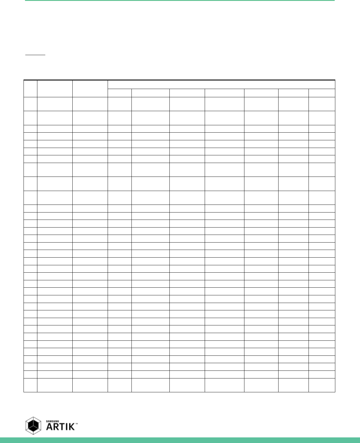
SIP0P5WRS50 MODULE GPIO ALTERNATE
FUNCTIONS
Table 11 describes the alternate functions that can be accessed using GPIOs that are available on the edge of the
SIP0P5WRS50 Module.
Table 11. Alternate functions of the SIP0P5WRS50 Module
PIN
#
Pin Name
Default
Function
Alternate Function
1
2
3
4
5
6
7
6
XGPIO22
XGPIO22
GPG2[6]
SerialFLASH_M
ONITOR_sf1_6
WB2AP_ETM_
DATA_OUT_13
WLBT_DEBUG_1
3
WAKE_EXT_IN
TG2[6]
-
-
7
XGPIO23
XGPIO23
GPG2[7]
SerialFLASH_M
ONITOR_sf1_7
WB2AP_ETM_
DATA_OUT_14
WLBT_DEBUG_1
4
WAKE_EXT_IN
TG2[7]
-
-
9
XJTAG_TRST_N
XJTAG_TRST_N
ETC0[0]
-
-
-
-
-
-
10
XJTAG_TMS
XJTAG_TMS
ETC0[1]
-
-
-
-
-
-
11
XJTAG_TCK
XJTAG_TCK
ETC0[2]
-
-
-
-
-
-
12
XJTAG_TDO
XJTAG_TDO
ETC0[4]
-
-
-
-
-
-
13
XJTAG_TDI
XJTAG_TDI
ETC0[3]
-
-
-
-
-
-
14
XEINT_0
XEINT_0
GPA0[0]
WAKE_EXT_INT
A0[0]
-
-
-
-
-
15
XEINT_2
XEINT_2
GPA0[2]
WAKE_EXT_INT
A0[2]
-
-
-
-
-
16
XEINT_1
XEINT_1
GPA0[1]
WAKE_EXT_INT
A0[1]
-
-
-
-
-
17
XI2C0_SCL
XI2C0_SCL
GPA1[0]
HSI2C_0_SCL
-
-
-
-
-
18
XI2C0_SDA
XI2C0_SDA
GPA1[1]
HSI2C_0_SDA
-
-
-
-
-
19
XI2C1_SCL
XI2C1_SCL
GPA1[2]
HSI2C_1_SCL
-
-
-
-
-
20
XI2C1_SDA
XI2C1_SDA
GPA1[3]
HSI2C_1_SDA
-
-
-
-
-
23
XDEBUG_RXD
XDEBUG_RXD
GPA3[0]
Xdebug_RXD
-
-
-
-
-
24
XDEBUG_TXD
XDEBUG_TXD
GPA3[1]
Xdebug_TXD
-
-
-
-
-
25
XPWMTOUT_5
XPWMTOUT_5
GPP2[5]
PWM_TOUT_5
-
-
-
-
-
26
XPWMTOUT_4
XPWMTOUT_4
GPP2[4]
PWM_TOUT_4
-
-
-
-
-
29
XPWMTOUT_3
XPWMTOUT_3
GPP2[3]
PWM_TOUT_3
-
-
-
-
-
30
XPWMTOUT_2
XPWMTOUT_2
GPP2[2]
PWM_TOUT_2
-
-
-
-
-
31
XPWMTOUT_1
XPWMTOUT_1
GPP2[1]
PWM_TOUT_1
COUNTER_0
UART_3_RTSn
-
-
-
33
XPWMTOUT_0
XPWMTOUT_0
GPP2[0]
PWM_TOUT_0
UART_3_CTSn
-
-
-
-
34
XGPIO27
XGPIO27
GPG3[3]
I2S_0_SDI
MCT1_TICK
-
-
-
-
35
XSPI0_CLK
XSPI0_CLK
GPP0[0]
SPI_0_CLK
-
-
-
-
-
36
XSPI0_MOSI
XSPI0_MOSI
GPP0[3]
SPI_0_MOSI
-
-
-
-
-
37
XSPI0_CSN
XSPI0_CSN
GPP0[1]
SPI_0_CSn
-
-
-
-
-
38
XSPI0_MISO
XSPI0_MISO
GPP0[2]
SPI_0_MISO
-
-
-
-
-
39
XUART1_RXD
XUART1_RXD
GPP0[4]
UART_1_RXD
UART_2_CTSn
-
-
-
-
40
XUART1_TXD
XUART1_TXD
GPP0[5]
UART_1_TXD
UART_2_RTSn
-
-
-
-
41
XUART2_RXD
XUART2_RXD
GPP0[6]
UART_2_RXD
-
-
-
-
-
42
XUART2_TXD
XUART2_TXD
GPP0[7]
UART_2_TXD
-
-
-
-
-
44
XUART3_RXD
XUART3_RXD
GPP1[6]
UART_3_RXD
-
-
-
-
-
45
XUART3_TXD
XUART3_TXD
GPP1[7]
UART_3_TXD
-
-
-
-
-
46
XGPIO12
XGPIO12
GPG1[4]
SerialFLASH_M
ONITOR_sf0_4
ALV_DBG[12]
WB2AP_ETM_D
ATA_OUT_03
WLBT_DEBUG
_03
WAKE_EXT_I
NTG1[4]
-
Samsung Semiconductor, Inc. SIP0P5WRS50 Module Datasheet
Samsung Confidential
Specifications in this document are tentative and subject to change.
17
PIN
#
Pin Name
Default
Function
Alternate Function
1
2
3
4
5
6
7
47
XGPIO9
XGPIO9
GPG1[1]
SPI_3_CSn
SerialFLASH_
MONITOR_sf0
_1
ALV_DBG[9]
WB2AP_ETM_
DATA_OUT_0
0
WLBT_DEB
UG_00
WAKE_EXT
_INTG1[1]
48
XGPIO11
XGPIO11
GPG1[3]
SPI_3_MOSI
SerialFLASH_
MONITOR_sf0
_3
ALV_DBG[11]
WB2AP_ETM_
DATA_OUT_0
2
WLBT_DEB
UG_02
WAKE_EXT
_INTG1[3]
49
XGPIO8
XGPIO8
GPG1[0]
SPI_3_CLK
SerialFLASH_
MONITOR_sf0
_0
ALV_DBG[8]
WB2AP_TRAC
E_CLK_OUT
WAKE_EXT_I
NTG1[0]
-
50
XGPIO10
XGPIO10
GPG1[2]
SPI_3_MISO
SerialFLASH_
MONITOR_sf0
_2
ALV_DBG[10]
WB2AP_ETM_
DATA_OUT_0
1
WLBT_DEB
UG_01
WAKE_EXT
_INTG1[2]
51
XGPIO7
XGPIO7
GPG0[7]
SPI_2_MOSI
ALV_DBG[7]
-
-
-
-
52
XGPIO6
XGPIO6
GPG0[6]
SPI_2_MISO
ALV_DBG[6]
-
-
-
-
53
XGPIO5
XGPIO5
GPG0[5]
SPI_2_CSn
ALV_DBG[5]
-
-
-
-
54
XGPIO4
XGPIO4
GPG0[4]
SPI_2_CLK
ALV_DBG[4]
-
-
-
-
55
XSPI1_MISO
XSPI1_MISO
GPP4[2]
SPI_1_MISO
-
-
-
-
-
56
XSPI1_CLK
XSPI1_CLK
GPP4[0]
SPI_1_CLK
-
-
-
-
-
57
XSPI1_MOSI
XSPI1_MOSI
GPP4[3]
SPI_1_MOSI
-
-
-
-
-
58
XSPI1_CSN
XSPI1_CSN
GPP4[1]
SPI_1_CSn
-
-
-
-
-
59
XGPIO1
XGPIO1
GPG0[1]
HSI2C_2_SDA
ALV_DBG[1]
-
-
-
-
60
XGPIO2
XGPIO2
GPG0[2]
HSI2C_3_SCL
ALV_DBG[2]
-
-
-
-
61
XGPIO3
XGPIO3
GPG0[3]
HSI2C_3_SDA
ALV_DBG[3]
-
-
-
-
62
XGPIO24
XGPIO24
GPG3[0]
I2S_0_BCLK
MCT0_INTlev
WB2AP_ETM_D
ATA_OUT_15
WLBT_DEBUG
_15
-
-
63
XGPIO25
XGPIO25
GPG3[1]
I2S_0_LRCK
MCT0_TICK
-
-
-
-
64
XGPIO26
XGPIO26
GPG3[2]
I2S_0_SDO
MCT1_INTlev
-
-
-
-
65
XGPIO18
XGPIO18
GPG2[2]
SerialFLASH_M
ONITOR_sf1_2
WB2AP_ETM_
DATA_OUT_09
WLBT_DEBUG_0
9
WAKE_EXT_IN
TG2[2]
-
-
66
XGPIO19
XGPIO19
GPG2[3]
SerialFLASH_M
ONITOR_sf1_3
WB2AP_ETM_
DATA_OUT_10
WLBT_DEBUG_1
0
WAKE_EXT_IN
TG2[3]
-
-
67
XGPIO20
XGPIO20
GPG2[4]
SerialFLASH_M
ONITOR_sf1_4
WLBT_UART_R
XD
WB2AP_ETM_D
ATA_OUT_11
WLBT_DEBUG
_11
WAKE_EXT_I
NTG2[4]
-
68
XGPIO21
XGPIO21
GPG2[5]
SerialFLASH_M
ONITOR_sf1_5
WLBT_UART_T
XD
WB2AP_ETM_D
ATA_OUT_12
WLBT_DEBUG
_12
WAKE_EXT_I
NTG2[5]
-
69
XGPIO15
XGPIO15
GPG1[7]
SerialFLASH_M
ONITOR_sf0_7
ALV_DBG[15]
WB2AP_ETM_D
ATA_OUT_06
WLBT_DEBUG
_06
WAKE_EXT_I
NTG1[7]
-
70
XGPIO16
XGPIO16
GPG2[0]
SerialFLASH_M
ONITOR_sf1_0
WB2AP_ETM_
DATA_OUT_07
WLBT_DEBUG_0
7
WAKE_EXT_IN
TG2[0]
-
-
71
XGPIO17
XGPIO17
GPG2[1]
SerialFLASH_M
ONITOR_sf1_1
WB2AP_ETM_
DATA_OUT_08
WLBT_DEBUG_0
8
WAKE_EXT_IN
TG2[1]
-
-
72
XGPIO13
XGPIO13
GPG1[5]
SerialFLASH_M
ONITOR_sf0_5
ALV_DBG[13]
WB2AP_ETM_D
ATA_OUT_04
WLBT_DEBUG
_04
WAKE_EXT_I
NTG1[5]
-
73
XGPIO14
XGPIO14
GPG1[6]
SerialFLASH_M
ONITOR_sf0_6
ALV_DBG[14]
WB2AP_ETM_D
ATA_OUT_05
WLBT_DEBUG
_05
WAKE_EXT_I
NTG1[6]
-
Samsung Semiconductor, Inc. SIP0P5WRS50 Module Datasheet
Samsung Confidential
Specifications in this document are tentative and subject to change.
18
SIP0P5WRS50 MODULE BOOTING SEQUENCE
The section describes the timing associated with powering up and resetting the SIP0P5WRS50 Module.
Figure 4. Booting and Reset Timing Relations
Samsung Semiconductor, Inc. SIP0P5WRS50 Module Datasheet
Samsung Confidential
Specifications in this document are tentative and subject to change.
19
SIP0P5WRS50 MODULE WI-FI ANTENNA STRUCTURE
The SIP0P5WRS50 Module has an chip Antenna and the feature is as below.
ISM 2.4GHz Wireless Device
Frequency range 2.4~2.485GHz
chip type Antenna
Size is 3.0 * 1.5 * 1.2 ㎣
SMT type
It is mounted on the PCB.
Antenna gain is as below.
Samsung Semiconductor, Inc. SIP0P5WRS50 Module Datasheet
Samsung Confidential
Specifications in this document are tentative and subject to change.
20
SIP0P5WRS50 MODULE ELECTRICAL SPECIFICATIONS
ABSOLUTE MAXIMUM RATING
Table 12. Absolute Maximum Ratings
PAD:[Pin#]
Symbol
Condition
Min
Typ
Max
Units
PAD:[27~28]
VIN
Input voltage VIN on the module
–
–
3.6
V
Other signal pad
Vundershoot
Undershoot voltage for I/O
-0.3
–
-
V
PAD:[31]
PWR_RST
–
-0.3
–
3.6
V
DC ELECTRICAL CHARACTERISTICS
Table 13. I/O DC Electrical Characteristics (PAD:5,6,14-26,29-31,33-42,44-73)
Parameter
Condition
Min
Typ
Max
Units
Tolerant External Voltage
VTOL
3.3 Power Off and On
–
–
3.60
V
High-Level Input Voltage
CMOS Interface
VIH
2.31
–
3.60
V
Low-Level Input Voltage
CMOS Interface
VIL
VDD=3.30V
-0.30
–
0.70
V
Hysteresis Voltage
ΔV
0.15
–
–
V
High-Level Input Current
Input Buffer
IIH
VIN=3.30V
VDD=3.30V Power On
-3.00
–
3.00
µA
VDD=3.30V Power Off &
SNS=0
-5.00
–
5.00
µA
Input Buffer with Pull-Down
VIN=3.30V
VDD=3.30V
13
40
90
µA
Low-Level Input Current
Input Buffer
IIL
VIN=0V
VDD=3.30V Power On and
Off
-3.00
–
3.00
µA
Input Buffer with Pull-Down
VIN=0V
VDD=3.30V
-13.00
–
-90.00
µA
Output High Voltage
VOH
IOH = 2.0mA, 4.0mA, 8.0mA and 12.0mA
2.64
–
3.30
V
Output Low Voltage
VOL
IOL = -2.0mA, -4.0mA, -8.0mA and -12.0mA
0
–
0.66
V
Output Hi-Z Current
VOZ
-5
–
5
µA
Input Capacitance
CIN
Any input and bi-directional buffers
–
–
5
pF
Table 14. I/O DC Electrical Characteristics (PAD:[2-5], ADC)
Parameter
Condition
Min
Typ
Max
Units
High Level Input Voltage
VIH
Guaranteed Logic High Level
1.26
–
1.80
V
Low Level Input Voltage
VIL
Guaranteed Logic Low Level
0
–
0.54
V
Output High Voltage
VOH
IOH=2mA, 4mA, 8mA and 12mA
1.44
–
1.80
V
Output Low Voltage
VOL
IOL=2mA, 4mA, 8mA and 12mA
0
–
0.36
V
Input Pull-Up Resistor Current
IRPU
VPAD=0
15
–
77
µA
Input Pull-Down Resistor Current
IRPD
VPAD=1.80
17
–
77
µA
Input Hysteresis
VH
–
0.18
–
–
V
Input Leakage Current for Non Tolerant Cells
IPAD
DVDD=1.80, VPAD=0 or 1.80V
-6
–
+6
µA
Off State Leakage Current
IOZ
DVDD=1.80, VPAD=0 or 1.80V
-6
–
+6
µA
Samsung Semiconductor, Inc. SIP0P5WRS50 Module Datasheet
Samsung Confidential
Specifications in this document are tentative and subject to change.
21
Table 15. Recommended Operating Conditions
Parameter
Symbol
Min
Typ
Max
Units
Main Power Supply: PAD:[27-28]
VIN_3P3
3.3
V
Maximum Operating Temperature
TO
-20
–
85
°C
Storage Temperature
TS
TBD
–
TBD
°C
Table 16. I/O Drive Strength
State
Currents: worst conditions VDD=3.30V
Units
DS0
DS1
SR: 0: Fast, 1: Slow
0
0
0/1
2
mA
0
1
0/1
4
mA
1
0
0/1
8
mA
1
1
0/1
12
mA
DC MODULE USE CASE CHARACTERISTICS
TBD
POWER SUPPLY REQUIREMENTS
TBD
ESD RATINGS
Table 17. ESD Ratings
Parameter
Min
Typ
Max
Units
ESD stress voltage Human Body Model (JEDEC)
-1.0
–
1.0
kV
ESD stress voltage Charged Device Model
–
250
–
V
RF ELECTRICAL CHARACTERISTICS
TBD
Samsung Semiconductor, Inc. SIP0P5WRS50 Module Datasheet
Samsung Confidential
Specifications in this document are tentative and subject to change.
22
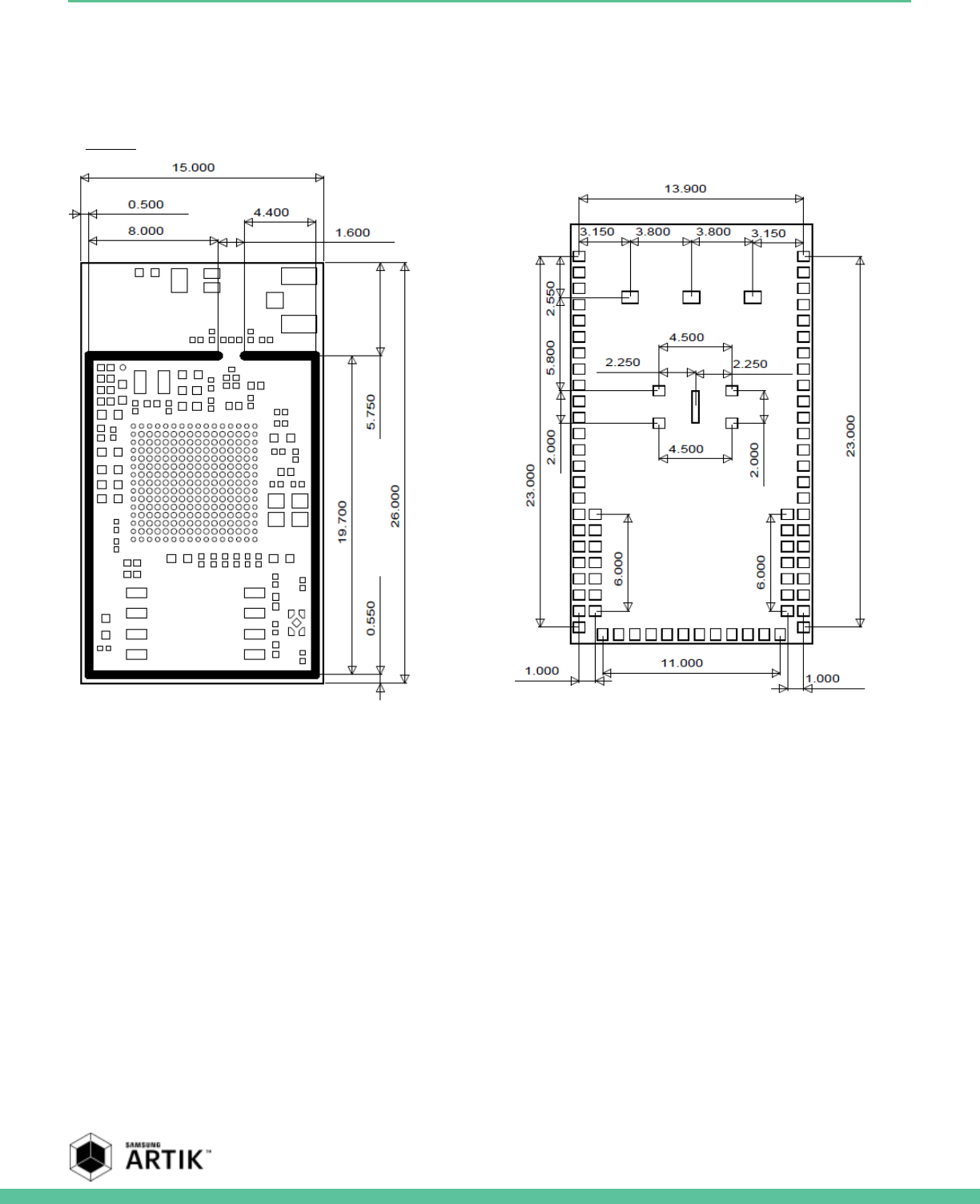
SIP0P5WRS50 MODULE MECHANICAL
SPECIFICATIONS
In Figure 5 the mechanical dimensions of the SIP0P5WRS50 Module are provided. All dimensions are in mm.
[TOP] [BOT]
Figure 5. SIP0P5WRS50 Module Mechanical Dimensions
Samsung Semiconductor, Inc. SIP0P5WRS50 Module Datasheet
Samsung Confidential
Specifications in this document are tentative and subject to change.
23
SIP0P5WRS50 MODULE FCC CERTIFICATION
This device complies with part 15 of the FCC Rules. Operation is subject to the following two conditions:
1. This device may not cause harmful interference, and
2. This device must accept any interference received, including interference that may cause undesired operation.
Caution: Any changes or modifications to the equipment not expressly approved by the party responsible for compliance
could void user’s authority to operate the equipment. This appliance and its antenna must not be co-located or operation in
conjunction with any other antenna or transmitter.
A minimum separation distance of 20cm must be maintained between the antenna and the person for this appliance to
satisfy the RF exposure requirements.
Instruction to OEM
This device complies with Industry Canada’s license-exempt RSSs. Operation is subject to the following two conditions:
1. This device may not cause interference and
2. This device must accept any interference, including interference that may cause
undesired operation of the device. This application and its antenna must not be co-located or operation in conjunction with
any other antenna or transmitter. A minimum separation distance of 20cm must be maintained between the antenna and
the person for this appliance to satisfy the RF exposure requirements. Host labeling requirement: “Contains transmitter
module
FCC ID: A3LSIP0P5WRS50
IC : 649E-SIP0P5WRS50
This device complies with part 15 of the FCC Rules. Operation is subject to the following two conditions:
1. This device may not cause harmful interference, and
2. This device must accept any interference received, including interference that may cause undesired operation.

Samsung Semiconductor, Inc. SIP0P5WRS50 Module Datasheet
Samsung Confidential
Specifications in this document are tentative and subject to change.
24
SIP0P5WRS50 MODULE ORDERING INFORMATION
Type
Order Number
Description
SIP0P5WRS50 Module
??
One SIP0P5WRS50 Module
SIP0P5WRS50 Evaluation Kit
??
One SIP0P5WRS50 Module
One EVK Board
One Wi-Fi Antenna
For volume ordering of evaluation kits, please contact a sales representative in your area or email sales@artik.io.

Samsung Semiconductor, Inc. SIP0P5WRS50 Module Datasheet
Samsung Confidential
Specifications in this document are tentative and subject to change.
25
LEGAL INFORMATION
INFORMATION IN THIS DOCUMENT IS PROVIDED IN CONNECTION WITH THE SAMSUNG ARTIK™ DEVELOPMENT KIT AND ALL
RELATED PRODUCTS, UPDATES, AND DOCUMENTATION (HEREINAFTER “SAMSUNG PRODUCTS”). NO LICENSE, EXPRESS OR
IMPLIED, BY ESTOPPEL OR OTHERWISE, TO ANY INTELLECTUAL PROPERTY RIGHTS IS GRANTED BY THIS DOCUMENT. THE
LICENSE AND OTHER TERMS AND CONDITIONS RELATED TO YOUR USE OF THE SAMSUNG PRODUCTS ARE GOVERNED
EXCLUSIVELY BY THE SAMSUNG ARTIK™ DEVELOPER LICENSE AGREEMENT THAT YOU AGREED TO WHEN YOU REGISTERED AS
A DEVELOPER TO RECEIVE THE SAMSUNG PRODUCTS. EXCEPT AS PROVIDED IN THE SAMSUNG ARTIK™ DEVELOPER LICENSE
AGREEMENT, SAMSUNG ELECTRONICS CO., LTD. AND ITS AFFILIATES (COLLECTIVELY, “SAMSUNG”) ASSUMES NO LIABILITY
WHATSOEVER, INCLUDING WITHOUT LIMITATION CONSEQUENTIAL OR INCIDENTAL DAMAGES, AND SAMSUNG DISCLAIMS
ANY EXPRESS OR IMPLIED WARRANTY, ARISING OUT OF OR RELATED TO YOUR SALE, APPLICATION AND/OR USE OF
SAMSUNG PRODUCTS INCLUDING LIABILITY OR WARRANTIES RELATED TO FITNESS FOR A PARTICULAR PURPOSE,
MERCHANTABILITY, OR INFRINGEMENT OF ANY PATENT, COPYRIGHT, OR OTHER INTELLECTUAL PROPERTY RIGHT.
SAMSUNG RESERVES THE RIGHT TO CHANGE PRODUCTS, INFORMATION, DOCUMENTATION AND SPECIFICATIONS WITHOUT
NOTICE. THIS INCLUDES MAKING CHANGES TO THIS DOCUMENTATION AT ANY TIME WITHOUT PRIOR NOTICE. THIS
DOCUMENTATION IS PROVIDED FOR REFERENCE PURPOSES ONLY, AND ALL INFORMATION DISCUSSED HEREIN IS PROVIDED
ON AN “AS IS” BASIS, WITHOUT WARRANTIES OF ANY KIND. SAMSUNG ASSUMES NO RESPONSIBILITY FOR POSSIBLE ERRORS
OR OMISSIONS, OR FOR ANY CONSEQUENCES FROM THE USE OF THE DOCUMENTATION CONTAINED HEREIN.
Samsung Products are not intended for use in medical, life support, critical care, safety equipment, or similar applications
where product failure could result in loss of life or personal or physical harm, or any military or defense application, or any
governmental procurement to which special terms or provisions may apply.
This document and all information discussed herein remain the sole and exclusive property of Samsung.
All brand names, trademarks and registered trademarks belong to their respective owners. For updates or
additional information about Samsung ARTIK™, contact the Samsung ARTIK™ team via the Samsung ARTIK™
website at www.artik.io.
Copyright © 2016 Samsung Electronics Co., Ltd.
All rights reserved. No part of this publication may be reproduced, stored in a retrieval system, or transmitted in any form or
by any means, electric or mechanical, by photocopying, recording, or otherwise, without the prior written consent of
Samsung Electronics.