Samsung Electronics Co WSM520V Audio transceiver module User Manual Users manual
Samsung Electronics Co Ltd Audio transceiver module Users manual
UserManual.wiki
>
Samsung Electronics Co
>
WSM520V User Manual
Users manual
Navigation menu
Upload a User Manual
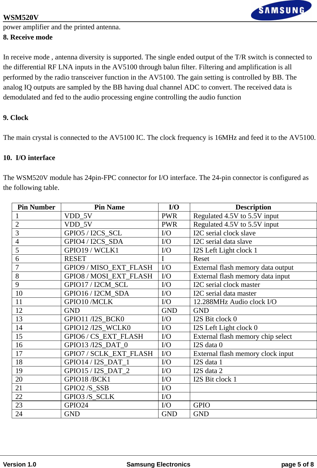
Namespaces
Wiki Guide
HTML
PDF
Info
Views
User Manual
Discussion / Help
Navigation