Sensitech T11012087 PART 15 CLASS B COMPUTING DEVICE PERIPHERAL User Manual
Sensitech, INC. PART 15 CLASS B COMPUTING DEVICE PERIPHERAL Users Manual
Users Manual

© SENSITECH INC. CONFIDENTIAL – CONTROLLED DOCUMENT
Page 1 of 83
A Carrier Corp. Company
PART NUMBER T82002163
REV A
TripStrip II
Hardware Specification Document
Sensitech Inc.
800 Cummings Center • Suite 258X
Beverly, MA 01915-6197

© SENSITECH INC. CONFIDENTIAL – CONTROLLED DOCUMENT Page 2 of 83
A Carrier Corp. Company
PART NUMBER T82002163
REV A
Federal Communications Commission (FCC) Statement
You are cautioned that changes or modifications not expressly approved by the part
responsible for compliance could void the user’s authority to operate the equipment
FCC-Class B
This equipment has been tested and found to comply with the limits for a class B
digital device, pursuant to part 15 of the FCC Rules. These limits are designed to
provide reasonable protection against harmful interference in a communications.
However, there is no guarantee that interference will not occur in particular
installation. If this equipment does cause harmful interference to radio or television
reception, which can be determined by turning the equipment off and on, the user is
encouraged to try to correct the interference by one or more of the following
measures:
- Reorient or relocate the receiving antenna.
- Increase the separation between the equipment and receiver.
- Connect the equipment into an outlet on a circuit different from that to which the
receiver is connected.
- Consult the dealer or an experienced radio/TV technician for help.
© SENSITECH INC. CONFIDENTIAL – CONTROLLED DOCUMENT
Page 3 of 83
A Carrier Corp. Company
PART NUMBER T82002163
REV A

© SENSITECH INC. CONFIDENTIAL – CONTROLLED DOCUMENT
Page 4 of 83
A Carrier Corp. Company
PART NUMBER T82002163
REV A
APPROVALS
Engineering:
Name: ______________________________
Date: ____________________________________________
Signature: ____________________________________________
Quality:
Name: _ ______________________
Date:
Signature: ______________________________________________
Manufacturing:
Name: _______________________________
Date:
Signature: ______________________________________________
Marketing:
Name: _____________________________
Date:
Signature: _________________________________________ ____
Technical Services:
Name: _____________________________
Date:
Signature: _________________________________________ ____

© SENSITECH INC. CONFIDENTIAL – CONTROLLED DOCUMENT
Page 5 of 83
A Carrier Corp. Company
PART NUMBER T82002163
REV A
Document Version Information ........................................................................................ 9
Organization of this Document ......................................................................................... 9
Executive Summary ........................................................................................................... 9
Device General Description............................................................................................... 9
Functional Description .............................................................................................................. 9
User Interface........................................................................................................................... 10
FRS in brief .............................................................................................................................. 12
Device Hardware Structure ............................................................................................. 13
General Hardware Information ............................................................................................. 13
Electrical Specification............................................................................................................ 13
Mode of Operation................................................................................................................... 13
Power Save Mode “Suspend State”........................................................................................ 15
Power Supply ........................................................................................................................... 15
Qty............................................................................................................................................17
Vendor .....................................................................................................................................17
SEIKO .................................................................................................................................17
SANYO ...............................................................................................................................17
PCB......................................................................................................................................17
Li-ION Charging...................................................................................................................... 21
LogicPD Card Engine.............................................................................................................. 23
Memory Controller Reset and Initialization......................................................................... 23
Memory Controller.................................................................................................................. 23
Memory Controller Operation ............................................................................................... 24
Stacked SDRAM and Flash Memory..................................................................................... 24
Stacked SDRAM...................................................................................................................... 24
Stacked Flash Memory............................................................................................................ 24
Synchronous Dynamic Memory (SDRAM) Interface........................................................... 26
Maximum Row Active Time (TRAS)..................................................................................... 26
Programmable Larger SDRAM Memory Space................................................................... 26
SDRAM State Machine ........................................................................................................... 27
Synchronous, Static, and Variable-Latency I/O (VLIO)...................................................... 29
Interfaces .................................................................................................................................. 29
Asynchronous Static Operation.............................................................................................. 29

© SENSITECH INC. CONFIDENTIAL – CONTROLLED DOCUMENT
Page 6 of 83
A Carrier Corp. Company
PART NUMBER T82002163
REV A
Asynchronous Flash Memory Interface................................................................................. 31
Memory Controller.................................................................................................................. 31
Synchronous Flash Memory ................................................................................................... 32
ROM Interface......................................................................................................................... 32
SRAM Interface Overview...................................................................................................... 33
Variable-Latency I/O Interface Overview............................................................................. 33
Memory Controller.................................................................................................................. 33
UARTs ...................................................................................................................................... 34
Overview................................................................................................................................... 34
Full-Function UART................................................................................................................ 35
Bluetooth UART ...................................................................................................................... 35
Compatibility with 16550A and 16750................................................................................... 35
Features .................................................................................................................................... 35
Signal Descriptions .................................................................................................................. 36
Operation.................................................................................................................................. 37
Reset.......................................................................................................................................... 38
USB Client Controller:............................................................................................................ 39
Overview................................................................................................................................... 39
Features .................................................................................................................................... 40
Signal Descriptions .................................................................................................................. 40
Bidirectional Signals................................................................................................................ 40
Operation.................................................................................................................................. 41
Peripheral Bus Interface and Control/Status Registers....................................................... 41
Suspend and Resume............................................................................................................... 43
Sleep Mode Operation............................................................................................................. 44
USB On-The-Go Operation .................................................................................................... 44
On-Chip OTG Transceiver Operation................................................................................... 45
Interface to External OTG Transceiver ................................................................................ 46
Interface to External Charge Pump Device........................................................................... 47
Memory Stick........................................................................................................................... 48
Overview................................................................................................................................... 48
Features .................................................................................................................................... 48
Signal Descriptions .................................................................................................................. 48

© SENSITECH INC. CONFIDENTIAL – CONTROLLED DOCUMENT
Page 7 of 83
A Carrier Corp. Company
PART NUMBER T82002163
REV A
Operation.................................................................................................................................. 48
Functional Description ............................................................................................................ 49
Interrupts.................................................................................................................................. 49
Memory Stick Insertion and Removal................................................................................... 49
Reset.......................................................................................................................................... 50
Power-Save Mode .................................................................................................................... 50
LogicPD Card Engine:................................................................................................51
Note: Our current Card Engine does support Ethernet...............................................54
TempTale Mini......................................................................................................................... 55
TempTale 4 (Epson TT4)........................................................................................................ 59
Command Transmission Paradigm........................................................................................ 59
Status Byte Definitions ............................................................................................................ 59
Communication Layer Descriptions ...................................................................................... 60
Data Recording Layer ............................................................................................................. 60
TempTale 4 (OKI TT4).................................................................................................... 62
Communications .............................................................................................................. 62
Establishing a Connection....................................................................................................... 63
Command Protocol.................................................................................................................. 65
TT4 Optical Interface Circuit................................................................................................. 69
LCD........................................................................................................................................... 69
Keypad...................................................................................................................................... 71
9.0 Battery Low Alert Function:.................................................................................72
10.0 Line Thermal Head Printer:.................................................................................72
11.0 Control Board......................................................................................................73
Device System Configuration Information............................................................................ 76
LogicLoader (LoLoTM).......................................................................................................... 76
LogicLoader Overview............................................................................................................ 76
LogicLoader Basics.................................................................................................................. 76
Using LogicLoader for Debugging......................................................................................... 76
Manufacturing Advantages with LoLo.................................................................................. 76
The LogicLoader Shell (loshTM).................................................................................... 77
Losh Overview.......................................................................................................................... 77
Losh Basics ............................................................................................................................... 77
Using Losh..................................................................................................................77

© SENSITECH INC. CONFIDENTIAL – CONTROLLED DOCUMENT
Page 8 of 83
A Carrier Corp. Company
PART NUMBER T82002163
REV A
Program Loading.............................................................................................................. 77
4.1 Understanding the Load Command ..................................................................................... 78
YAFFS (Yet Another Flash File System)........................................................................... 79
8.1 YAFFS Overview ................................................................................................................ 79
8.2 Working with YAFFS in LogicLoader................................................................................ 79
8.2.1 Developing a Partition Scheme..........................................................................79
8.2.2 Formatting YAFFS Partitions............................................................................80
8.2.3 Adding YAFFS Type Partitions.........................................................................80
8.2.4 Mounting the Partition.......................................................................................80
8.2.5 Accessing YAFFS Partitions in an OS..............................................................81
8.3 Summary..................................................................................................................................
Device System Configuration/Programming.............................................................................
Explanation of Script...................................................................................................................
Appendix: .....................................................................................................................................
SAMPLE PRINT-OUT...............................................................................................................................
List of Error Messages (12.9.08).................................................................................................

© SENSITECH INC. CONFIDENTIAL – CONTROLLED DOCUMENT
Page 9 of 83
A Carrier Corp. Company
PART NUMBER T82002163
REV A
Document Version Information
Document Version
Functional Requirement Specifications T85000530, Rev. A
Hardware Specifications T82002163, Rev. A
Firmware
Organization of this Document
This document outlines the TripStripII’s specifications in detail. It describes each aspect of the unit’s
functionality and how the hardware is configured.
Executive Summary
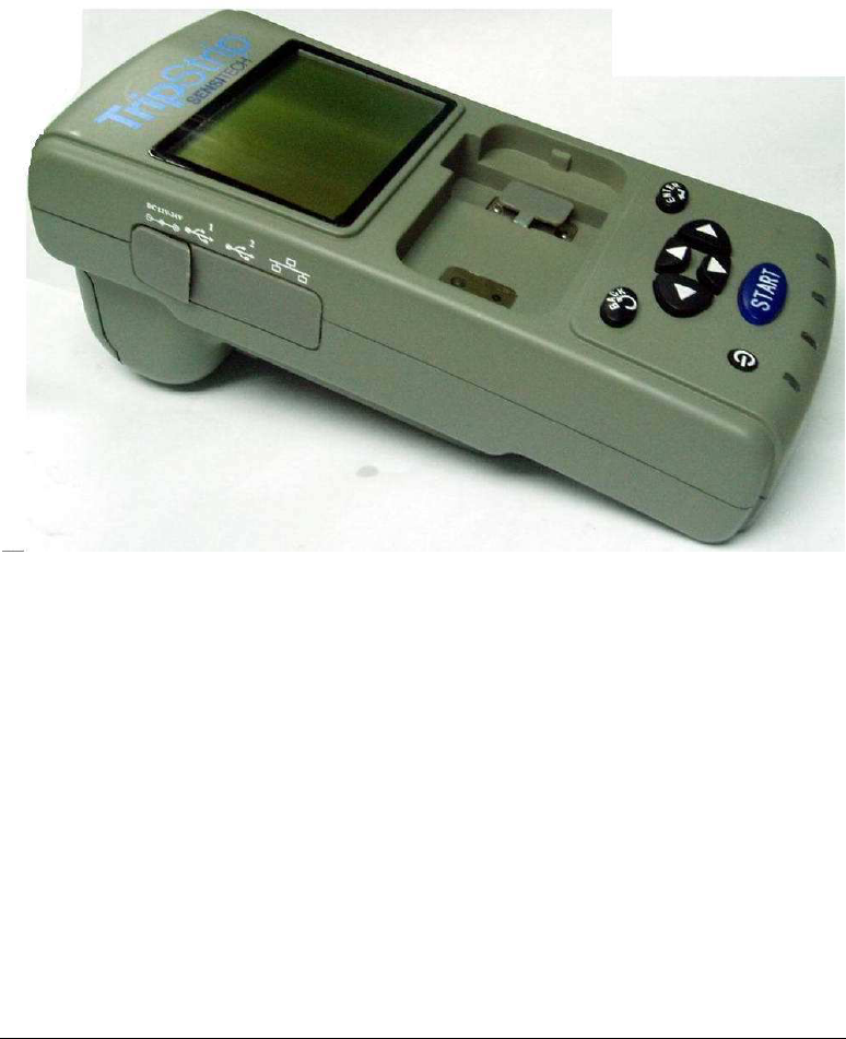
The TripStrip II is a handheld thermal printer which is capable of portable or desktop use. This particular
model supersedes the previous TripStrip platform with many functional enhancements such as it will allow
the download of 16K TempTale data loggers, TempTale Mini and all TempTale variants. An integral
monochrome 4 inch LCD was added to provide the user with a quick view of the monitor data such as
display summary and graph as well as menu navigation for unit functionality. The TripStrip II also has a
USB host and client to allow further communication channels.
Device General Description
Functional Description
The following is an overview of the TripStrip II and its features.
Note: Input voltage range is 12VDC – 24VDC.
The TripStrip II remote data printer generates graphs from all TempTale 4 variants (2k and 16k) and
TempTale Mini 2k. To be specific, TT4 Ambient, TT4 Humidity, TT4 Probe and Dual Sensor, TT4 BIO,
TT4 Dry Ice Probe, TT4 Probeless Dry Ice, and TT4 RF. The TripStrip II is available as a Li-ION
rechargeable battery-powered unit, shipped fully charged and ready for use. The battery may be recharged
by the 15VDC switcher adapter, 12VDC automobile car adapter, or 24VDC Trailer Truck adapter.
© SENSITECH INC. CONFIDENTIAL – CONTROLLED DOCUMENT
Page 10 of 83
A Carrier Corp. Company
PART NUMBER T82002163
REV A
User Interface
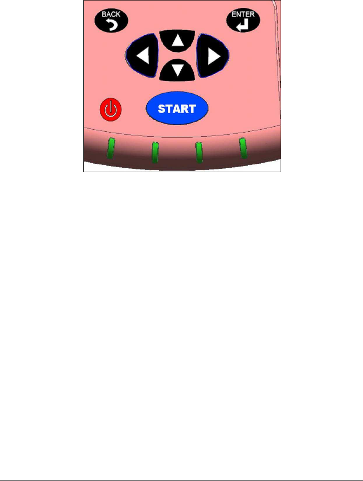
Power Charge Paper Out Low Batt
User presses the Power Button and the unit is powered ON and the Power LED is ON. The
Sensitech application program appears momentarily. The user is now able to download any TT4 (2k/16k)
or TTmini; except TT4 USB. To download a TT4 unit, the user may place a TT4 on the optical interface
and press START. To download a TTmini, the user may connect the TTmini to the RS232 DB9 connector
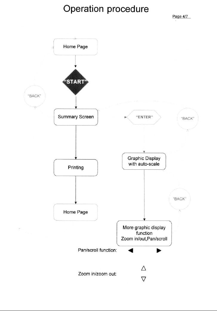
and press START.
Once the user presses START, the TSII auto-detects which UART to begin downloading from.
The summary data will appear first and the unit will begin printing (if option is enabled via Menu), then the
user will have an option of displaying the graph on the LCD by pressing the ENTER key which defaults to
Auto Scale Mode. The user will have the ability to Zoom In/Out of the graph. Zoom interval will be Max
Trip Length / 5, regardless of the EEPROM size or monitor type.
Please note: For the ZOOM feature, no matter what type of monitor or EEPROM size, the TSII
will take the max trip length and divide it by 5. However, please note due to the resolution, if the monitor
data size is less than (approximately) 512K then this will not apply. The user will only see the graph screen
and will not be able to ZOOM. (If the EEPROM has more than or equal to 64 points then it will have the
zoom feature).
© SENSITECH INC. CONFIDENTIAL – CONTROLLED DOCUMENT
Page 11 of 83
A Carrier Corp. Company
PART NUMBER T82002163
REV A

© SENSITECH INC. CONFIDENTIAL – CONTROLLED DOCUMENT
Page 12 of 83
A Carrier Corp. Company
PART NUMBER T82002163
REV A
FRS in brief
To re-design the current TripStrip TempTale Remote Printer that provides hardcopy printouts of
time/temperature data and related information from TempTale monitors.
The current version of the product, while suitable in many applications for most customers has
several deficiencies that impede further adoption of TempTale monitoring programs. In addition, the
product is RoHS compliant.
The TripStrip is an ancillary product, designed purely as an accessory in support of in-bound and
closed loop TempTale monitoring programs, primarily in the food and supermarket segments. In many
cases the product is offered to customers as a free or deeply discounted instrument in support of large
volume TempTale programs. Within this context product volumes are anticipated to be in the 100-500
units/year range.
The objectives of this project are:
• Eliminate the current TripStrip deficiencies and upgrade the product feature set per the
requirements described below.
• Maintain or reduce product costs at/from current level
• Provide product/system “architectural” features consistent with current and potential future
product line strategies.
• Minimize development and tooling/capital expense (the product is low-volume, with in-direct ROI
potential)

© SENSITECH INC. CONFIDENTIAL – CONTROLLED DOCUMENT
Page 13 of 83
A Carrier Corp. Company
PART NUMBER T82002163
REV A
Device Hardware Structure
General Hardware Information
Electrical Specification
1.1 SWITCHING POWER SUPPLY
Input Voltage: AC 100~240V
Frequency:50/60Hz
Input Current: 1500mA.
Output Voltage: DC 15V
Output Current: DC 4000mA
1.2 DC Input: 12-24V
* 15VDC Wall Adapter
* 12 VDC automobile DC adapter
* 24 VDC trailer truck DC adapter
1.2.1 Input current: 2-5A
1.2.2Power Consumption: approximately 15W
1.3. Charging
Max Charging Current:3A
Charging Voltage: 8.4V +/- 0.1V
Charging Time: 3.5hr
Discharging current: 2-6A
Discharging time: 3hr/2A
Environment Specification
Operating Temperature: 0-45°C
Storage Temperature: 0-45°C
Operating Humidity: 0-99%
Mechanical Specification
Cabinet Size: 270(L)*135(W)*110(H) mm
Weight: Approximately 1100g
Color: Grey
Mode of Operation
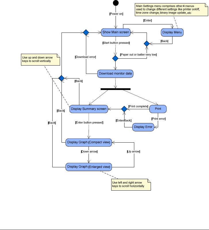
The user presses the platen release button on the unit to load a 50mm paper roll into the frontend of the
TripStripII unit. The user will then Power ON device using the POWER button on the Keypad.
SENSITECH, INC. window appears. Now, the user is able to navigate through the menus or
download/print a TempTale 4 monitor or TempTale Mini. A hand strap located on the rear of the unit
provides the user optimal portability support.LED status indicators are visible on the front end of the unit or
Power, LowBatt, Charging, and Paper out.
© SENSITECH INC. CONFIDENTIAL – CONTROLLED DOCUMENT
Page 14 of 83
A Carrier Corp. Company
PART NUMBER T82002163
REV A
2k monitor = 11 seconds to download the data and an additional 49 seconds to print
16k monitor = 1 minute to download and an additional 6 minutes to print

© SENSITECH INC. CONFIDENTIAL – CONTROLLED DOCUMENT
Page 15 of 83
A Carrier Corp. Company
PART NUMBER T82002163
REV A
Power Save Mode “Suspend State”
Suspend state is the PXA270 SOM’s hardware power down state, allowing for lower power consumption.
The Suspend state is designed to reduce power consumption while the PXA270 is waiting for an event such
as a keyboard input. The suspend state is entered using Logic BSP’s by asserting the nSUSPEND signal or
through software. The PXA270 processor is put into Standby Mode. All power supplies remain active.
System context is retained. Internal clocks are stopped except RTC. An internal or external wakeup event
can cause the processor to transition back to Run Mode.
IMPORTANT NOTE: Although Suspend consumes less power than Run state, it consumes more power
than the Standby state. Thus, on a power failure, the PXA270 system will actually leave the Suspend state
and transition to the Standby state (the same thing occurs on a SW_nRESET).
During suspend state, the unit powers OFF the LCD backlight, printer head, and printer control board.
When user reinitiates activity, the unit returns to full active state of all devices.
If needed, user may engage the Reset Button located on the right-side of the unit.
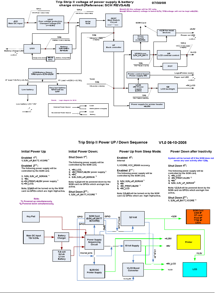
Power Supply
The following are methods a user is able to supply power to the TripStripII device to charge/operate:
1. Dual Voltage 120/60 Hz (220/50 Hz) – 15VDC Wall Adapter
2. 12 VDC automobile DC adapter
3. 24 VDC trailer truck DC adapter
Internally, the TripStripII power supply consists of:
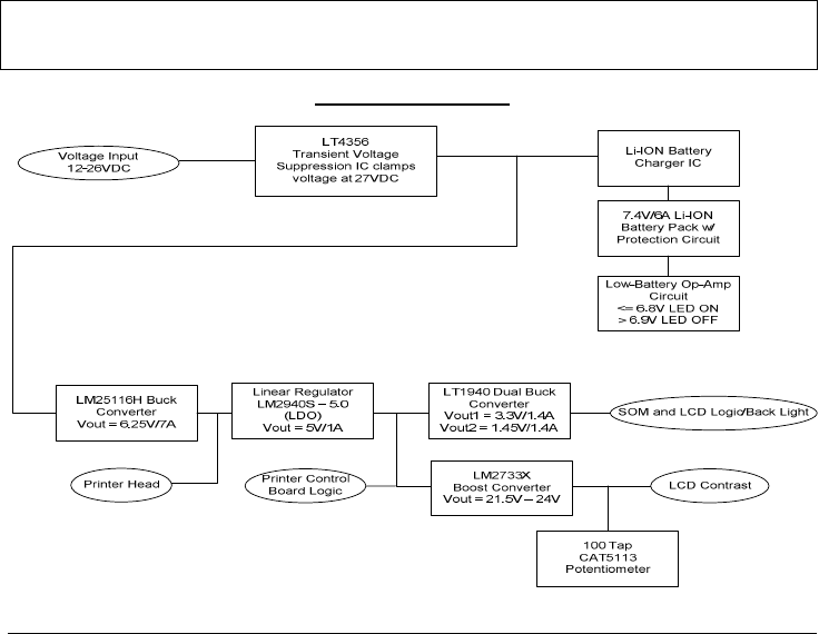
1. LT4356-1, Overvoltage Protection Regulator and Inrush Limiter IC
• The LT4356-1 surge stopper protects loads from high voltage transients.
• It regulates the output during an overvoltage event, such as load dump in automobiles, by
controlling the gate of an external N-Channel MOSFET.
• The output is limited to a safe value thereby allowing the loads to continue functioning.
• The LT4356-1 also monitors the voltage drop between the VCC and SNS pins to protect against
overcurrent faults.
• An internal amplifier limits the current sense voltage to 50mV.
• In either fault condition, a timer is started inversely proportional to MOSFET stress.
• If the timer expires, the /FLT pin pulls low to warn of an impending power down. If the condition
persists, the
MOSFET is turned off.
2. LTC4006, 4A, High Efficiency, Standalone Li-Ion Battery Charger
• The LTC4006 is a complete constant-current/constant voltage charger controller for 2-, 3- or 4-cell
lithium batteries.
• The PWM controller is a synchronous, quasi-constant frequency, constant off-time architecture
that will not generate audible noise even when using ceramic capacitors.
• Charging current is programmable with a single sense resistor to ±4% typical accuracy.
• Charging current can be monitored as a representative voltage at the IMON pin.
• A timer, programmed by an external resistor, sets the total charge time or is reset to 25% of total
charge time after C/10 charging current is reached.
• Charging automatically resumes when the cell voltage falls below 3.9V/cell.

© SENSITECH INC. CONFIDENTIAL – CONTROLLED DOCUMENT
Page 16 of 83
A Carrier Corp. Company
PART NUMBER T82002163
REV A
• Fully discharged cells are automatically trickle charged at 10% of the programmed current until
the cell voltage exceeds 2.5V/cell.
• Charging terminates if the low-battery condition persists for more than 25% of the total charge
time.
• The LTC4006 includes a thermistor sensor input that suspends charging if an unsafe temperature
condition is detected and automatically resumes charging when the battery temperature returns to
within safe limits.
• The LTC4006 charges a 7.4VDC/6A battery pack.
• The battery pack contains 6 Li-ION cells (2S3P topology).
• The battery pack internally contains a Li-ION protection circuit.
Design Note:
Note during prototype testing, we supplied 15VDC input to the TSII and the L105 inductor on the
LTC4006 Charger Circuit reaches approximately 60-62C during charging (in open air). We will look
into adding a passive heat sink to dissipate some of the heat. This was also the case when we supplied
24VDC input to the TSII.
After charge is complete, the L105 inductor will reach 29-30 degrees C (in open air). An NTC
Thermistor was used to measure the temperature of the L105 inductor.
3. LM339 Low Power Low Offset Voltage Quad Comparator. (Low-battery detection):
• The circuit is comprised of two Compartors. If the Vin(+) terminal is Low and the Vin(-) terminal
is High, then the output is Low (current will flow). However if the Vin(+) terminal is High and the
Vin(-) terminal is Low, then the output is High (current will not flow).
Therefore, If the Load in the variable input (5 – 27VDC) is <= 6.5VDC, then the Low Batt LED will be
ON. However, if the variable input is >6.8VDC, then the Low Batt LED is OFF. The other input VB =
3.3VDC, which is a fixed voltage input.
4. Battery Pack Protection Circuit (model: 033A-BXA)
• Function: Over charge detection, Over discharge detection, Over current detection, Short
detection.
• ELECTRIC CHARACTERISTICS (@ 25C)
1) Over charge detection voltage: 8.5V +/- 50mV
2) Over charge release voltage: 8.1V +/- 100mV
3) Over discharge detection voltage: 4.8V +/- 160mV
4) Over current detection: 4.00A ~ 7.00A
5) Over charge detection delay time: 0.55S~2.06S
6) Over discharge detection delay time: 67~141ms
7) Over current detection delay time: 6.3~14.7ms
8) Consumption current
– Operating mode : Max 14.2 µA
– Power - saving mode : Max0.2µA.

© SENSITECH INC. CONFIDENTIAL – CONTROLLED DOCUMENT
Page 17 of 83
A Carrier Corp. Company
PART NUMBER T82002163
REV A
PARTS LIST
Location Description Specification Size Qty Vendor
U1 PROTECTION
IC S-8232ABFT-T2 TSSOP-8 1 SEIKO
Q1 N-CH FET FTD2017A TSSOP-8 1 SANYO
R1,R2R
3,R4
CHIP
RESISTOR 1Kohm (J) 1608 Size 4
R5 CHIP
RESISTOR 4.7Mohm (J) 1608 Size 1
YAGEO,TAMA,
KAMAYA,
ROHM ,SEM ,
Any Approved Vendor
R6 CHIP
POWER
RESISTOR R020ohm 6331 Size 1
YAGEO,TAMA,
KAMAYA,
ROHM ,SEM ,
Any Approved Vendor
C1,C2,C3 CHIP
CAPACITOR 0.1uF 25V (Z ) 1608 Size 3
YAGEO,PHYCOMP,
KYOCERA,ROHM,
SAMWHA,SEM,
Any Approved Vendor
PCB FR-4,1oz,0.6t,
2Layer 40*7 1
5. LM25116 Wide Range Synchronous Buck Controller
• The LM25116 is a synchronous buck controller intended for step-down regulator applications
from a high voltage or widely varying input supply.
• The control method is based upon current mode control utilizing an emulated current ramp.
• Current mode control provides inherent line feed-forward, cycle by cycle current limiting and ease
of loop compensation.
• The use of an emulated control ramp reduces noise sensitivity of the pulse-width modulation
circuit, allowing reliable control of very small duty cycles necessary in high input voltage
applications.
• The LM25116 drives external high-side and low-side NMOS power switches with adaptive dead-
time control.
• A user-selectable diode emulation mode enables discontinuous mode operation for improved
efficiency at light load conditions.
• A low quiescent current shutdown disables the controller and consumes less than 10µA of total
input current.

© SENSITECH INC. CONFIDENTIAL – CONTROLLED DOCUMENT
Page 18 of 83
A Carrier Corp. Company
PART NUMBER T82002163
REV A
• Additional features include a high voltage bias regulator, automatic switch-over to external bias
for improved efficiency, thermal shutdown, frequency synchronization, cycle by cycle current
limit and adjustable line under-voltage lockout.
• The device is available in a power enhanced TSSOP-20 package featuring an exposed die attach
pad to aid thermal dissipation
• 7-42VDC input voltage and converts it to 6.25VDC/7A.
• This voltage output is for the Print Head.
6. LT1940, Dual Monolithic 1.4A, 1.1MHz Step-Down Switching Regulator
• The LT1940 is a dual current mode PWM step-down DC/DC converter with internal 2A power
switches.
• Both converters are synchronized to a single 1.1MHz oscillator and run with opposite phases,
reducing input ripple current.
• The output voltages are set with external resistor dividers, and each regulator has independent
shutdown and soft-start circuits.
• Each regulator generates a power-good signal when its output is in regulation, easing power
supply sequencing and interfacing with microcontrollers and DSPs.
• The LT1940’s 1.1MHz switching frequency allows the use of tiny inductors and capacitors,
resulting in a very small dual 1.4A output solution.
• Constant frequency and ceramic capacitors combine to produce low, predictable output ripple
voltage.
• With its wide input range of 3.6V to 25V
• Converts it to 3.3V/1.4A and 1.45V/1.4A. 1.45V is for VCORE which is the processor’s core
voltage.
• 3.3V is for the remaining voltages such as I/O and peripheral supply voltage.
7. LM2940, 1A Low Dropout Regulator
• The LM2940 positive voltage regulator features the ability to source 1A of output current with a
dropout voltage of typically 0.5V and a maximum of 1V over the entire temperature range.
• Furthermore, a quiescent current reduction circuit has been included which reduces the ground
current when the differential between the input voltage and the output voltage exceeds
approximately 3V.
• The quiescent current with 1A of output current and an input-output differential of 5V is therefore
only 30 mA.
• Higher quiescent currents only exist when the regulator is in the dropout mode (VIN − VOUT ≤
3V).
• The linear regulator (LDO) take a maximum of 26VDC input voltage and converts it to 5V/1A.
• This voltage output is for printer control board logic and boost converter.
8. LM2733, 0.6/1.6 MHz Boost Converters With 40V Internal FET Switch in SOT-23
• The LM2733 switching regulators are current-mode boost converters operating fixed frequency of
1.6 MHz (“X” option).
• The use of SOT-23 package, made possible by the minimal power loss of the internal 1A switch,
and use of small inductors and capacitors result in the industry's highest power density.
• Protection is provided through cycle-by-cycle current limiting and thermal shutdown.
• Internal compensation simplifies design and reduces component count.
• Boost Converter takes 3.3VDC from the Buck Converter and boosts the voltage output to
17.8VDC to 25.5VDC.
© SENSITECH INC. CONFIDENTIAL – CONTROLLED DOCUMENT
Page 19 of 83
A Carrier Corp. Company
PART NUMBER T82002163
REV A
9. The CAT5113 is a single digitally programmable 10K potentiometer designed as a electronic
replacement for mechanical potentiometers.
• The CAT5113 contains a 100-tap series resistor array connected between two terminals RH and
RL.
• An up/down counter and decoder that are controlled by three input pins, determines which tap is
connected to the wiper, RW.
• The wiper setting, stored in nonvolatile memory, is not lost when the device is powered down and
is automatically reinstated when power is returned.
• The wiper can be adjusted to test new system values without affecting the stored setting.
• Wiper-control of the CAT5113 is accomplished with three input control pins, /CS, U/D, and /INC.
• The /INC input increments the wiper in the direction which is determined by the logic state of the
U/D input.
• The /CS input is used to select the device and also store the wiper position prior to power down.
• The digitally programmable potentiometer can be used as a three-terminal resistive divider or as a
two terminal variable resistor.
During the event of transitioning the Chip Select from a low to a high state, this will Store the LCD
Contrast Voltage in Memory.
During the event of transitioning the Chip Select from a low to a high state and Increment low, this will not
store the value and return to standby.
(J1C.23 Card Engine) GPIO 99 = Up/Down
(J1C.88 Card Engine) GPIO 36 = Chip Select
(J1C.25 Card Engine) GPIO 27 = Increment
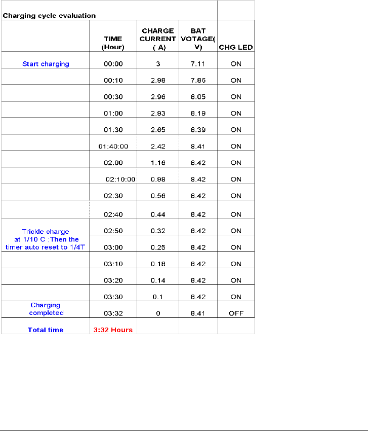
See block diagram below:
© SENSITECH INC. CONFIDENTIAL – CONTROLLED DOCUMENT
Page 20 of 83
A Carrier Corp. Company
PART NUMBER T82002163
REV A
© SENSITECH INC. CONFIDENTIAL – CONTROLLED DOCUMENT
Page 21 of 83
A Carrier Corp. Company
PART NUMBER T82002163
REV A
Li-ION Charging
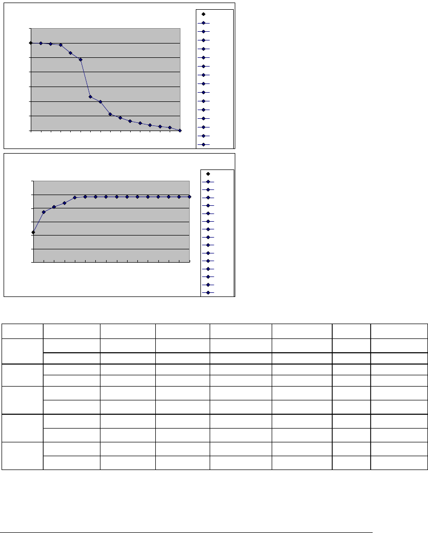
1.Charging cycle evaluation (Battery is empty before this charge) Chager IC is 4006 and CHG indicator
available only
Conditions: Fully Discharge the battery before the charging cycle test. The input power supply is 15V and
charging current is 3A
Remark: The Max. charging time is around 3 hours. According to specification the charging time is limited
to 3 hours ,when charge current is 1/10c then the timer is auto reset ¼ T; So the total time max is 3:45
hours ;and the CHG LED will turn off when charging completed.
© SENSITECH INC. CONFIDENTIAL – CONTROLLED DOCUMENT
Page 22 of 83
A Carrier Corp. Company
PART NUMBER T82002163
REV A
Charging Current Vs time
0
0.5
1
1.5
2
2.5
3
3.5
00:00 01:00 02:00 02:40 03:10 03:32
Current (A)
00:00
00:10
00:30
01:00
01:30
01:40:00
02:00
02:10:00
02:30
02:40
02:50
03:00
03:10
03:20
03:30
03:32
Battery Voltage During charging
6
6.5
7
7.5
8
8.5
9
00:00
00:30
01:30
02:00
02:30
02:50
03:10
03:30
Battery Voltage (V)
00:00
00:10
00:30
01:00
01:30
01:40:00
02:00
02:10:00
02:30
02:40
02:50
03:00
03:10
03:20
03:30
03:32
1) Power suppply efficiency evaluation
Input Voltage (V) Input Current (A) Input PD(W) Output Voltage (V) Output Current(A) Output PD(W) Efficiency(%)
12 2.630 31.56 7.2 3.88 27.936 88.51711027
24 1.400 33.6 7.5 3.8 28.5 84.82142857
8.4 3.530 29.652 7.14 4 28.56 96.31728045
24 1.330 31.92 7.14 4 28.56 89.47368421
7.13 1.120 7.9856 4.98 1 4.98 62.36225205
7.14 0.550 3.927 4.98 0.5 2.49 63.40718105
7.08 0.300 2.124 3.29 0.5 1.645 77.44821092
7.06 0.570 4.0242 3.28 1 3.28 81.50688336
7.09 0.162 1.14858 1.44 0.5 0.72 62.68609936
7.08 0.304 2.15232 1.436 1 1.436 66.71870354
1.45VOutput(LT1
940)
CHARGE
7.2V Output
(LM3075)
5V
output(LM2940s-
5.0)
3.3V
Output(LT1940)
NOTE: THIS WILL NEED TO CHANGE BECAUSE THE LM3075 BUCK CONVERTER HAS BEEN REPLACED.

© SENSITECH INC. CONFIDENTIAL – CONTROLLED DOCUMENT
Page 23 of 83
A Carrier Corp. Company
PART NUMBER T82002163
REV A
2) External Power adapter loading evaluation
Charging at 3A only
Charging3A+Loading1.
45v&0.5A
Charging3A+Loading1.
45v&0.5A+3.3V&0.5A
Charging3A+Loading3.3V
&1A+7.2V&3.0A
Charging3A+Loading3.3
V&1A+7.2V&3.3A
AC/DC Adapter
Outpout Voltage(V)
14.9 14.770 14.89 14.71 14.58
AC/DC ADAPTER
OUTPUT CURRENT
(A)
2.32 2.390 2.56 4.58 4.74
PD(W) 34.568 35.300 38.1184 67.3718 69.1092
Note:The adapter 's max PD is 70W.
LogicPD Card Engine
Memory Controller Reset and Initialization
The SDRAM interface is disabled on reset. Reset values for the boot ROM are determined by BOOT_SEL.
BOOT ROM is immediately available for reading upon exit from reset, and all memory interface control
registers are available for writing.
Memory Controller
The internal and external memory-interface structures for the PXA27x processor will be described in detail
below. Memory-related registers that configure the memory controller for data transfers to and from static
and dynamic memory devices are also described.
The external memory-bus interface for the PXA27x processor supports SDRAM, synchronous, and
asynchronous burst-mode and page-mode flash memory, page-mode ROM, SRAM, variable latency
I/O (VLIO) memory, PC Card, and CompactFlash expansion memory. Memory types are
programmable through the memory-interface configuration registers (see Table 6-44).
Memory requests are placed in a four-deep processing queue and processed in the order they are
received.
Features
The memory controller provides the following features:
• Interfaces to internal synchronous flash and SDRAM devices
• Interfaces to four partitions of SDRAM
• Interfaces to up to 1.0 Gbytes of SDRAM
• Supports 1.8-V JEDEC LP-SDRAM operation at 104 MHz
• Interfaces to six partitions of static memory. Four of these six partitions can be synchronous
flash memory.
• Interfaces to up to 384 Mbytes of flash memory
• Interfaces to two sockets of PC Card memory
• Allows an alternate bus master to take control of the bus
• Places the SDRAMs into self-refresh mode before entering sleep, standby, deep-sleep, and

© SENSITECH INC. CONFIDENTIAL – CONTROLLED DOCUMENT
Page 24 of 83
A Carrier Corp. Company
PART NUMBER T82002163
REV A
frequency-change modes
• Provides signals and controls for fly-by DMA transfers
• Supports non-volatile memory configured as bank 0 from either 16- or 32-bit devices
• Provides three independent output clocks (SDCLK<2:0>) that can be turned on/off separately
and can be programmed to be free-running. The clocks can be the same frequency or half the
frequency of the input clock, CLK_MEM. One clock (SDCLK<0>) can also be programmed
as one quarter of the input-clock frequency. A fourth output clock (SDCLK<3>) depends on
configuration bits used to control SDCLK<0>.
• Provides a programmable power-down mode for saving power
Memory Controller Operation
The processor has three different memory spaces: SDRAM, static memory, and PC Card space.
SDRAM has four partitions, static memory has six partitions, and PC Card space has two partitions
(or sockets). When user software performs a memory burst across the boundary between any two
adjacent partitions, the configurations for each partition must be identical. They must have the
same external bus width, burst length, and so forth.
In theory, the partitions can be different types of memory sharing the same configuration
characteristics. In practice, cross-partition memory bursts are conducted only when the two
partitions hold the same memory type. A typical case is a transfer across two SDRAM partitions, 0
and 1, which are mandated to have the same characteristics.
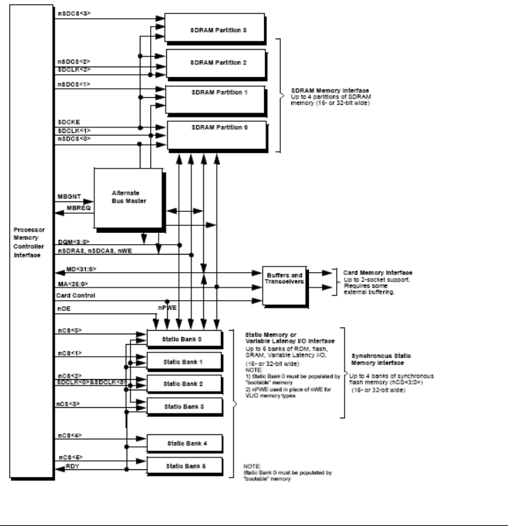
Figure 6-1 is a block diagram of the maximum configuration of the memory controller.
Stacked SDRAM and Flash Memory
This section describes memory types that may be supported in the PXA271 and PXA272
processors.
Stacked SDRAM
On the Intel® PXA271 processor, SDRAM is stacked and connected to SDRAM partition 0. On
systems using the Intel® PXA271 processor, external SDRAM memory chips must not exist within
the same SDRAM partition pair as that of the internal stacked SDRAM. This could cause negative
signal reflection to the stacked SDRAM device.
For the Intel® PXA271 processor stacked SDRAM, the Intel® PXA27x processor memory
controller must be programmed to multiplex the SDRAM address lines out differently because the
address lines to the stacked SDRAM are not connected to the usual MA<24:10> lines. The
MDCNFG[STACKx] field on a Intel® PXA271 processor must be programmed to 0b01 to send the
SDRAM address out on MA<24:23,13:1> for stacked 16-bit SDRAM of this product.
For a non stacked part (Intel® PXA270 processor) or flash only stacked part (Intel® PXA272
processor) the MDCNFG[STACKx] field must be programmed to 0b00 to send the SDRAM
address out on MA<24:10>.
Stacked Flash Memory
A fourth SDCLK, SDCLK<3> is driven by the memory controller, to be used in the PXA271 and
PXA272 processors containing stacked flash devices. SDCLK<3> is a buffer duplicate of
© SENSITECH INC. CONFIDENTIAL – CONTROLLED DOCUMENT
Page 25 of 83
A Carrier Corp. Company
PART NUMBER T82002163
REV A
SDCLK<0> and does not have any control bits of its own to turn it on or off. Use the buffer
strength field associated with SDCLK<3> to turn off SDCLK<3> if there is no stacked flash in the
system. This buffer strength setting is located in the BSCNTR2 register.
Static partitions 0 and 1 may contain stacked flash. The memory controller must be aware of which
static memory partitions contain stacked flash. This is programmed in the SA1111[SXSTACK]
field. When a flash device is being written to, the nCS and nWE signals swap functionality from a normal
flash write to an off-chip
device. This is shown by timing diagrams in the Intel® PXA27x Processor Family EMTS.
Figure 6-1. General Memory Interface Configuration

© SENSITECH INC. CONFIDENTIAL – CONTROLLED DOCUMENT
Page 26 of 83
A Carrier Corp. Company
PART NUMBER T82002163
REV A
Synchronous Dynamic Memory (SDRAM) Interface
The processor supports the JEDEC synchronous dynamic memory (SDRAM) interface. The
SDRAM interface supports four 16-bit or 32-bit wide partitions of SDRAM. Each partition is
allocated 64 or 256 Mbytes of the internal memory map. The actual size of each partition depends
on the SDRAM configuration used. The four partitions are divided into two partition pairs: the 0/1
pair and the 2/3 pair. Both partitions in a pair must be identical in size and configuration. Pairs 0/1
and 2/3 can be different. For example, the 0/1 pair can be 100-MHz SDRAM on a 32-bit data bus,
while the 2/3 pair can be 50-MHz SDRAM on a 16-bit data bus.
The SDRAM interface includes the following:
• Four partition selects, nSDCS<3:0>
• Four byte mask signals, DQM<3:0>
• 15 multiplexed bank/row/column address signals, MA<24:10>, MA<24:23,14:2>, or
MA<24:23,13:1>, depending on the MDCNFG[STACKx] setting
• One write enable, nWE
• One column-address strobe (nSDCAS)
• One row-address strobe (nSDRAS)
• One clock enable (SDCKE)
• Two clocks (SDCLK<2:1>)
The processor performs auto-refresh (CBR) during normal operation and supports self-refreshing
SDRAM during sleep, deep-sleep, standby, and frequency-change modes. An SDRAM autopower-
down mode bit (MDREFR[APD]) can be set so that the two clocks (SDCLK<2:1>) and the
clock-enable signal (SDCKE) to SDRAM are automatically de-asserted whenever none of the
corresponding partitions is being accessed.
Each possible SDRAM section of the memory map is referred to as a partition, to distinguish them
from banks internal to SDRAM devices.
Maximum Row Active Time (TRAS)
The maximum amount of time that any SDRAM row can be active is defined as TRASMAX. When
programming MDREFR[DRI], ensure that the refresh cycle time is less than TRASMAX because it is
not monitored by the memory controller.
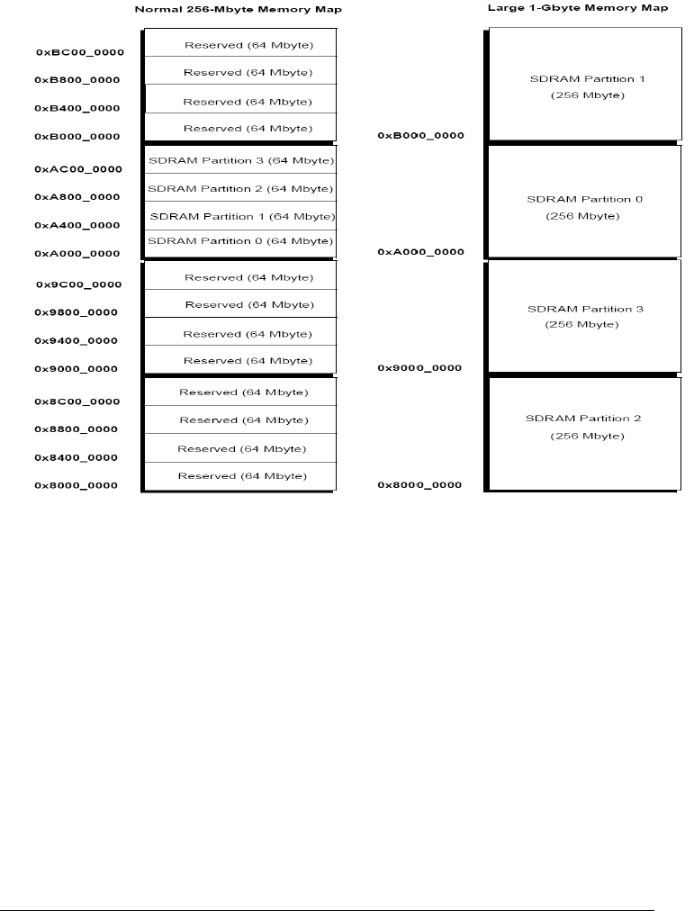
Programmable Larger SDRAM Memory Space
The read/write MDCNFG register contains control bits for configuring the SDRAM for larger
SDRAM configurations than fit in the 64-Mbyte SDRAM partitions. Refer to Table 6-23 for
configuration programming. Figure 6-2 shows the programmable option for the SDRAM memory
space.
© SENSITECH INC. CONFIDENTIAL – CONTROLLED DOCUMENT
Page 27 of 83
A Carrier Corp. Company
PART NUMBER T82002163
REV A
Programmable SDRAM Memory Map Options (Figure below):
SDRAM State Machine
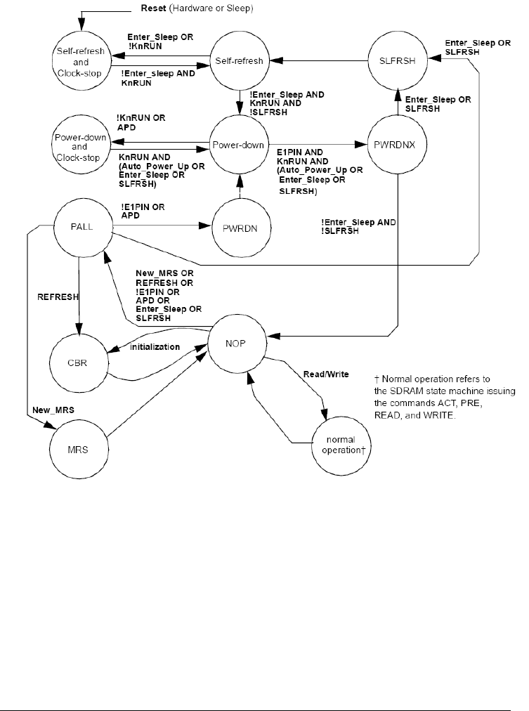
Figure 6-4 shows the SDRAM controller states and transitions associated with powering on the
PXA27x processor and the SDRAMs properly. Transitions are determined by the overall memory
controller state and a few SDRAM power-down, self-refresh status, and control bits. The states that
involve multiple SDRAM devices are self-refresh and clock-stop, self-refresh, SLFRSH,
PWRDNX, power-down, power-down and clock-stop, PWRDN, PALL, and MRS. The states that
involve single SDRAM partitions are ACT, PRE, READ, and WRITE. The MRS command is sent
once to configure partition pair 0/1 and a separate MRS command is sent only once to configure
partition pair 2/3. The auto-refresh command is issued to memory in the same partition pair at the
same time. Therefore, the chip-select signals representing the partition pair are asserted at the same
time when the MRS command and auto-refresh is issued from the memory controller to a specific
partition pair.
© SENSITECH INC. CONFIDENTIAL – CONTROLLED DOCUMENT
Page 28 of 83
A Carrier Corp. Company
PART NUMBER T82002163
REV A
SDRAM Power-ON State Machine (figure below):
Sleep, deep-sleep, standby, or frequency-change requests cause the SDRAM state machine to enter
the self-refresh and clock-stop state. Software must then complete the appropriate reset procedure. Clearing
MDREFR[E1PIN] and MDREFR[KnRUN] provides software control of the SDRAM memory system low-
power modes.
Note: (1) Use these modes with extreme caution, because the resulting states prohibit automatic toggles
from mode register set, read, write, and refresh commands.
The Auto_Power_Down and Auto_Power_Up transitions (made possible by setting the APD bit in
MDREFR) provide a completely automatic alternative for minimizing power consumption in the
SDRAM system.
(2) Some companion chips require the clock to be present at all times.
Use the following prioritization scheme for transitions out of the NOP state. If enabled with the
APD bit, the Auto_Power_Down transition occurs when none of the higher priority transitions are
asserted. The Auto_Power_Up transitions occur when refresh, New_MRS, or read/write is asserted
during the Power_Down state.

© SENSITECH INC. CONFIDENTIAL – CONTROLLED DOCUMENT
Page 29 of 83
A Carrier Corp. Company
PART NUMBER T82002163
REV A
Highest Priority- ”Enter Sleep”
“Set_SLFRSH”
“Clear_E1PIN”
“Refresh”
“New_MRS”
“Read/Write”
Lowest Priority - “Auto_Power_Down”
KnRUN = MDREFR[K1RUN] OR MDREFR[K2RUN]
Auto_Power_Down = MDREFR[APD]
Clear_E1PIN = !(MDREFR[E1PIN])
Set_SLFRSH = MDREFR[SLFRSH]
Enter_Sleep = Sleep/Deep-Sleep/Standby/ Frequency Change Request and no more
transactions to process
Auto_Power_Up = Read/Write is asserted during the power-down state OR New_MRS
OR Refresh OR !(MDREFR[APD])
Synchronous, Static, and Variable-Latency I/O (VLIO)
Interfaces
The static memory and VLIO interfaces have six chip selects (nCS<5:0>) and 26 bits of byte
address (MA<25:0>) for accesses of up to 64 Mbytes of memory in each of six banks. Alternately,
a mode is available to support up to two 128-Mbyte chip selects (nCS<1:0>) with 26 bits of halfword
address (MA<0>, MA<25:1>) and two 64-Mbyte chip selects (nCS<5:4>) with 25 bits of
byte address (MA<25:0>). This programmable option resides in the Static Memory Configuration
register SA1110[SXENX]. Each chip select is individually programmed to select one of the
supported static memory types.
• Non-burst ROM or flash memory (Section 6.4.3.2) is supported on each of
nCS<5:0>
• Burst ROM or flash memory with non-burst writes (Section 6.4.3.2) is
supported on each of nCS<5:0>
• SRAM is supported on each of nCS<5:0>
• Variable-latency I/O is supported on each of nCS<5:0>
• Synchronous flash memory is supported on each of nCS<3:0>
The four synchronous-flash memory partitions (nCS<3:0>) are divided into two partition pairs: the
0/1 pair and the 2/3 pair. Both partitions in a pair must be identical in size and configuration. The
two pairs can be different. For example, the 0/1 pair can be 66-MHz synchronous flash memory on
a 32-bit data bus while the 2/3 pair is 33-MHz synchronous flash memory on a 16-bit data bus.
The VLIO interface differs from SRAM in that it allows the use of the data-ready input signal,
RDY, to insert a variable number of wait states. For all static memory types, each chip select can be
configured individually to a 16-bit or 32-bit wide data bus. The nOE signal is asserted on reads, the
nPWE signal is asserted on writes to VLIO devices, and the nWE signal is asserted on writes to all
other static devices, both synchronous and asynchronous. For SRAM and VLIO, DQM<3:0> are
byte enables for both reads and writes. When the processor comes out of reset, it begins to fetch
and execute instructions at address 0x00, which corresponds to memory selected by nCS<0>,
which is the required location of the boot ROM. The BOOT_SEL pin determines the width of the
boot memory.
Asynchronous Static Operation
The static-memory interface is comprised of six chip selects, nCS<5:0>. These six chip selects are
© SENSITECH INC. CONFIDENTIAL – CONTROLLED DOCUMENT
Page 30 of 83
A Carrier Corp. Company
PART NUMBER T82002163
REV A
configurable for the following:
• Non-burst ROM or flash memory
• Burst ROM or flash memory
• SRAM
• VLIO devices
The VLIO interface differs from SRAM in that it allows the use of a data-ready input signal, RDY,
to insert a variable number of memory-cycle wait states. The data bus width for each chip-select
region can be programmed to be 16- or 32-bit. The nCS<3:0> signals are also configurable for
synchronous static memory. The following list describes the use of nOE,
nWE, and nPWE:
• nOE is asserted for all reads.
• nWE is asserted for flash memory and SRAM writes.
• nPWE is asserted for VLIO writes.
For SRAM and VLIO implementations, DQM<3:0> are used for the write byte-enables, where
DQM<3> corresponds to the MSB. The processor supplies 26 bits of byte address for access of up
to 64 Mbytes per chip select. This byte address is sent out on the 26 external address pins. If the
byte address is unimportant for an application, the lower bit must be truncated for 16-bit systems
and the lower two bits must be truncated for 32-bit systems. For reads, the byte address bits is 0.
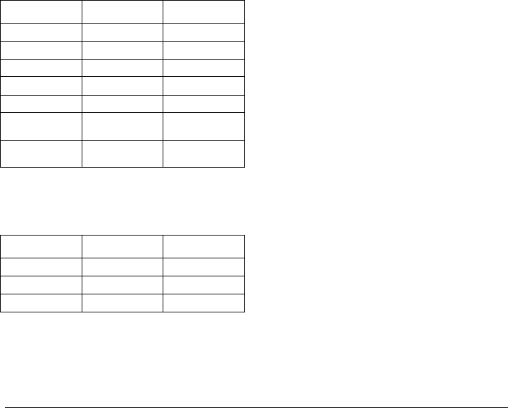
For writes, the byte address bits are summarized in Table 6-10 and Table 6-11.
Table 6-10. 32 Bit Byte Address Bits MA <1.0>
for Writes Based on DQM <3.0>
Transaction DQM<3:0> MA<1:0>
Word 0b0000 0b00
Byte 0 0b1110 0b00
Byte 1 0b1101 0b01
Byte 2 0b1011 0b10
Byte 3 0b0111 0b11
Lower half
word 0b1100 0b00
Upper half
word 0b0011 0b10
Table 6-11. 16-Bit Byte Address Bit MA <0> for Writes Based on DQM <1.0>
Transaction DQM<1:0> MA<0>
Half word 0b00 0b0
Byte 0 0b10 0b0
Byte 1 0b01 0b1
The MSCx[RTx] fields specify the type of memory:
• Non-burst ROM or flash memory
• SRAM
• VLIO
• Burst-of-four ROM or flash memory

© SENSITECH INC. CONFIDENTIAL – CONTROLLED DOCUMENT
Page 31 of 83
A Carrier Corp. Company
PART NUMBER T82002163
REV A
• Burst-of-eight ROM or flash memory
The MSCx[RBWx] fields specify the bus width for the memory space selected by nCS<5:0>. If a
16-bit bus width is specified, transactions occur across data pins MD<15:0>. Use the BOOT_SEL
pin or SXCNFG register to configure nCS<3:0> for synchronous static memory.
Asynchronous Flash Memory Interface
The MSCx[RDFx] bit fields define the latency for each read access of non-burst flash memory or
the first read access of burst flash memory. The same bit field also controls the nWE de-assertion
time during a write cycle to flash memory. The MSCx[RDN] field controls subsequent read access
times to burst flash memory. The MSCx[RRR] bit field calculates the minimum period from the
nCS signal de-assertion following a read or write and before the start of the read from a different
memory.
The following requirements apply to reads from flash memory:
• Because flash memory defaults to read-array mode, burst reads from it are permitted, which
allows instruction caching and burst reads (DMA and USB host) from flash memory.
• Some areas of flash memory might not permit burst reads. When attempting to read from these
areas, do not attempt burst reads. Consult the flash-memory data sheet for more information.
Table 6-10. 32-Bit Byte Address Bits MA<1:0> for Writes Based on DQM<3:0>
Transaction DQM<3:0> MA<1:0>
Word 0b0000 0b00
Byte 0 0b1110 0b00
Byte 1 0b1101 0b01
Byte 2 0b1011 0b10
Byte 3 0b0111 0b11
Lower half word 0b1100 0b00
Upper half word 0b0011 0b10
Table 6-11. 16-Bit Byte Address Bit MA<0> for Writes Based on DQM<1:0>
Transaction DQM<1:0> MA<0>
Half word 0b00 0b0
Byte 0 0b10 0b0
Byte 1 0b01 0b1
Memory Controller
• Software must partition commands and data, then write the commands to flash memory before
a read. The memory controller does not insert any commands before flash-memory reads.
The following requirements apply to writes to flash memory:
• Flash memory space must be uncacheable and unbuffered.
• Burst writes to flash memory do not exist. Writes to flash memory must be exactly the width of
the populated flash devices on the data bus and must be a burst length of one write (for
instance, no byte writes to a 32-bit bus, no word writes to a 16-bit bus, no writes of 2 bytes to a
32-bit bus, no writes of 1 byte to a 16-bit bus). The allowable writes are 2 bytes to a 16-bit bus
and 4 bytes to a 32-bit bus.
• For writes to flash memory, the command and data must be given to the memory controller in
separate write instructions. The first instruction carries the command; the next carries the data.
• Software must partition commands and data and write them to flash memory in the appropriate
sequence. The memory controller does not insert any commands before flash-memory writes.
• Because burst writes to flash memory cannot occur, the DMA controller and USB host
controller must never write to flash memory. Burst writes to flash memory are not performed.

© SENSITECH INC. CONFIDENTIAL – CONTROLLED DOCUMENT
Page 32 of 83
A Carrier Corp. Company
PART NUMBER T82002163
REV A
Synchronous Flash Memory
This section describes how to interface with synchronous flash memory. Synchronous flashmemory
operation resets to asynchronous mode (page mode for reads and asynchronous singleword
writes). The only way the system can enter synchronous mode (burst-timing synchronous
reads and asynchronous single-word writes) is through the Read Configuration register (RCR).
Therefore, at boot time, synchronous flash memory operates the same as asynchronous boot ROM.
Table 6-12 shows sample programming values for the RCR Synchronous Flash Memory register to
ensure proper operation of synchronous flash memory.
Use the values in Table 6-12 as a reference only. Consult the data sheet for the actual part being
used. Determine the frequency-configuration code based on the CLK-to-output delay, the CLK
period, and the nADV-to-output delay timing parameters for the flash device.
Table 6-12. Sample Read Programming Values for Synchronous Flash Memory (Sheet 1 of 2)
Bits Field Name Value to Program†
2:0 BURST LENGTH 0b010 = 8-word burst
5:3 reserved 0b000
6 CLOCK CONFIGURATION
0b1 = Use rising edge of clock
7 BURST SEQUENCE 0b1 = Linear burst order (Intel burst order is not
supported)
8 WAIT CONFIGURATION Not applicable—The processor ignores nWAIT from
the flash device.
9 DATA OUTPUT
CONFIGURATION 0b0 = Hold data for one clock
10 reserved 0b0
†
for configuration register
Table 6-12. Sample Read Programming Values for Synchronous Flash Memory (Sheet 2 of 2)
Bits Field Name Value to Program†
0b010 -> Code 2 (CAS latency 3)
0b011 -> Code 3 (CAS latency 4)
0b100 -> Code 4 (CAS latency 5)
13:11
FREQUENCY
CONFIGURATION 0b101 -> Code 5 (CAS latency 6)
0b110 -> Code 6 (CAS latency 7)
Choose this value based on the “AC Characteristics—
Read-Only
Operation” section of the flash-memory device data
sheet.
14 reserved 0b0
15 READ MODE 0b0 = Synchronous operation 0b1 = Asynchronous
operation
†
for configuration register
ROM Interface
The processor provides programmable timing for both burst and non-burst ROMs. The value of

© SENSITECH INC. CONFIDENTIAL – CONTROLLED DOCUMENT
Page 33 of 83
A Carrier Corp. Company
PART NUMBER T82002163
REV A
MSCx[RDF] defines the latency (in memory clock cycles) for the first and all subsequent data
beats from non-burst ROMs and the first data beat from a burst ROM. The value of MSCx[RDN]
defines the latency for the burst data beats after the first for burst ROMs. Specifying the
MSCx[RRR] value allows a delay on the next access to a different memory space to allow time for
the current ROM to three-state the data bus. MSCx[RRR] must be programmed with the maximum
TOFF value divided by two, as specified by the ROM manufacturer.
MSC0<15:0> is selected when the address space corresponding to nCS<0> is accessed.
SRAM Interface Overview
The processor provides a 16- or 32-bit synchronous SRAM interface that uses the DQM pins for
byte enables on writes. Bits nCS<5:0> select the SRAM bank to be used. nOE is asserted on reads
and nWE is asserted on writes. Address bits MA<25:0> allow up to 64 Mbytes of SRAM per bank
to be addressed.
The RDF fields in the MSCx registers define the latencies for a read access. The MSCx[RDN] field
controls the nWE low time during a write cycle. MSCx[RRR] is defined as the minimum time from
nCS de-assertion to the beginning of a read or write access of any memory bank
Any DMA mode that does not increment the address is not supported for SRAM reads or writes.
DCMDx[INCSRCADDR] and DCMDx[INCTRGADDR] clear cause the address not to be
incremented. This DMA mode is not supported for SRAM. The only valid memory types for this
mode are VLIO and PC Card/CompactFlash devices.
Variable-Latency I/O Interface Overview
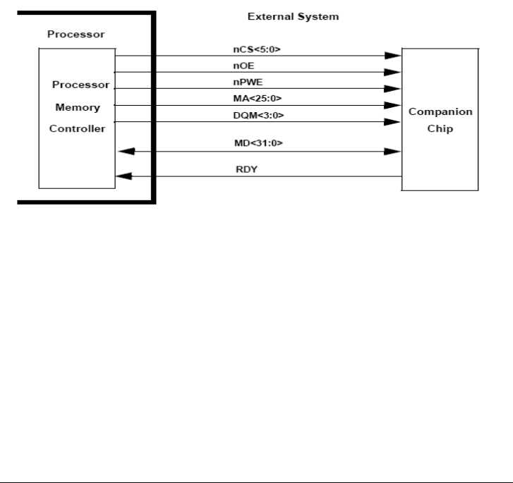
When a companion chip is used as a VLIO device, its functionality is similar to that of an SRAM
with the additional ability to insert a variable number of wait states through the RDY pin. VLIO
can be used in the memory space for any of the six static memory locations (nCS<5:0>) by
programming the corresponding MSCx[RTx] to 0b100.
13:11 FREQUENCY CONFIGURATION
0b010 -> Code 2 (CAS latency 3)
0b011 -> Code 3 (CAS latency 4)
0b100 -> Code 4 (CAS latency 5)
0b101 -> Code 5 (CAS latency 6)
0b110 -> Code 6 (CAS latency 7)
Choose this value based on the “AC Characteristics—Read-Only
Operation” section of the flash-memory device data sheet.
14 reserved 0b0
15 READ MODE 0b0 = Synchronous operation
0b1 = Asynchronous operation
Table 6-12. Sample Read Programming Values for Synchronous Flash Memory
Bits Field Name Value to Program
Memory Controller
VLIO read accesses differ from SRAM read accesses in that nOE toggles for each beat of a burst.
The first nOE assertion occurs two CLK_MEM cycles after the chip select, nCSx, is asserted. For
VLIO writes, nPWE is used instead of nWE, which allows SDRAM refreshes to execute while
performing the VLIO transfers.
© SENSITECH INC. CONFIDENTIAL – CONTROLLED DOCUMENT
Page 34 of 83
A Carrier Corp. Company
PART NUMBER T82002163
REV A
For both reads and writes from and to VLIO, clearing DCMDx[INCSRCADDR] and
DCMDx[INCTRGADDR] causes the source and target addresses not to be incremented to the
VLIO interface, which allows port-type VLIO chips to interface with the processor. The only valid
memory types for this DMA mode are VLIO and PC Card/CompactFlash devices.
For writes to VLIO, if all byte enables are turned off (masking out the data, DQM = 0b1111), then
the write enable is suppressed (nPWE = 1) for this write-beat to VLIO. This suppression can cause
a period when nCS is asserted but neither nOE nor nPWE is asserted, which would happen if there
is a write of one beat to VLIO with all byte enables turned off. In this case, the memory controller
ignores the RDY signal. The RDY signal must not be asserted late if it is to still be asserted, which
could interfere with any following transfers. If the VLIO device does not see an nOE or a nPWE, it
must not change the state of RDY, keeping it either asserted or de-asserted.
With the exception of the case above, and when entering a frequency change, the memory
controller indefinitely waits for the RDY signal to be asserted, which can hang the system if the
external VLIO is not responding. To prevent indefinite hangs, set the watchdog timer when starting
a VLIO transfer; a watchdog reset occurs if no response is received from the VLIO device.
Figure 6-5. Variable-Latency I/O Diagram
UARTs
This chapter describes the universal asynchronous receiver/transmitter (UART) serial ports
included in the PXA27x processor. The serial ports are controlled using direct-memory access
(DMA) or programmed I/O. The PXA27x processor has three UARTs: full-function (FFUART),
Bluetooth (BTUART), and standard (STUART). All UARTs use the same programming model.
Overview
Each serial port contains a UART and a slow infrared-transmit encoder and receive decoder that
conform to the IrDA serial-infrared specification.1
Each UART performs serial-to-parallel conversion on data characters received from a peripheral
device or a modem and parallel-to-serial conversion on data characters received from the
processor. The processor can read a UART’s complete status during functional operation. Status
information includes the type and condition of transfer operations and error conditions (parity,
overrun, framing, or break interrupt) associated with the UART.
Each serial port operates in either FIFO or non-FIFO mode. In FIFO mode, a 64-byte transmit
FIFO holds data from the processor until it is transmitted on the serial link, and a 64-byte receive

© SENSITECH INC. CONFIDENTIAL – CONTROLLED DOCUMENT
Page 35 of 83
A Carrier Corp. Company
PART NUMBER T82002163
REV A
FIFO buffers data from the serial link until it is read by the processor. In non-FIFO mode, the
transmit and receive FIFOs are bypassed.
Each UART includes a programmable baud-rate generator that can divide the input clock by 1 to
(216 – 1). This produces a 16X clock that can be used to drive the internal transmit and receive
logic. Software can program interrupts to meet its requirements, which minimizes the number of
computations required to handle the communications link. Each UART operates in an environment
that is either controlled by software and can be polled or is interrupt-driven.
All three UARTs support the 16550A and 167502 functions, but are slightly different in the features
supported.
Full-Function UART
The FFUART supports modem-control capability. The maximum baud rate is 921,600 bps.
Bluetooth UART
The BTUART is a high-speed UART that supports baud rates up to 921,600 bps and can be
connected to a Bluetooth module. It supports the functions in the feature list, but supports only two
modem control pins (nCTS and nRTS).
1. Infrared Data Association, Serial Infrared Physical Layer Link Specification, October 17, 1995, Version
1.1
2. The 16550A was originally produced by National Semiconductor Inc. The 16750 is produced as the
TL16C750 by Texas Instruments.
The STUART supports all functions in the feature list, but does not support modem-control
capability. The maximum baud rate is 921,600 bps.
Compatibility with 16550A and 16750
The UARTs are functionally compatible with the 16550A and 16750 industry standards. Each
UART supports most of the 16550A and 16750 functions, as well as the following features:
• DMA requests for transmit and receive data services
• Slow infrared-asynchronous interface
• Non-return-to-zero (NRZ) encoding/decoding function
• 64-byte transmit/receive FIFO buffers
• Programmable receive FIFO trigger threshold
• Auto baud-rate detection
• Auto flow
Features
The UARTs share the following features:
• Functionally compatible with the 16550A and 16750
• Ability to add or delete standard asynchronous communication bits (start, stop, and parity) in
the serial data
• Independently controlled transmit, receive, line status, and data-set interrupts
• Programmable baud-rate generator that allows the internal clock to be divided by 1 to (216 – 1)
to generate an internal 16X clock
• Modem control functions (nCTS, nRTS, nDSR, nDTR, nRI, and nDCD)
• Auto-flow capability controls data I/O without generating interrupts:
— nRTS (output) controlled by UART receive FIFO
— nCTS (input) from modem controls UART transmitter
• Fully programmable serial interface:
— 5-, 6-, 7-, or 8-bit characters
— Even, odd, and no-parity detection

© SENSITECH INC. CONFIDENTIAL – CONTROLLED DOCUMENT
Page 36 of 83
A Carrier Corp. Company
PART NUMBER T82002163
REV A
— 1, 1½, or 2 stop-bit generation
— Baud-rate generation up to 921 kbps for all UARTs
— False start-bit detection
• 64-byte transmit FIFO
• 64-byte receive FIFO
• Complete status-reporting capability
• Ability to generate and detect line breaks
• Internal diagnostic capabilities that include:
— Loopback controls for communications-link fault isolation
— Break, parity, and framing-error simulation
• Fully prioritized interrupt system controls
• Separate DMA requests for transmit and receive data services
• Slow infrared asynchronous interface that conforms to the Infrared Data Association (IrDA)
specification
Signal Descriptions
Table 10-1 lists and describes each external signal that is connected to a UART module. The pins
transmit digital CMOS-level signals and are connected to the PXA27x processor through GPIOs.
Refer to Section 24, “General-Purpose I/O Controller” for details on the GPIOs.
Table 10-1. UARTs I/O Signal Descriptions (Sheet 1 of 2)
Name
Type Description
RXD Input
Serial Input- Serial data input to the receive
shit register. In infrared mode, it is connected
to the infrared receiver input. This signal is
present on all three UARTs.
TXD Output
Serial Output—Serial data output to the communications-link peripheral, modem, or
data set. The TXD signal is set to the logic 1 state upon a reset operation. It is connected
to the output of the infrared transmitter in infrared mode. This signal is present on all
three UARTs.
nCTS
Input
Clear to Send—When low, indicates that the modem or data set is ready to exchange
data. The nCTS signal is a modem status input, and its condition can be tested by reading
bit 4 (CTS) of the Modem Status register (MSR). MSR[CTS] is the complement of the
nCTS signal. MSR[DCTS] indicates whether the nCTS input has changed state since the
last time MSR was read. nCTS has no effect on the transmitter. This signal is present on
the FFUART and BTUART. When MSR[CTS] changes state and the modem-status
interrupt is enabled, an interrupt is generated. Non-Auto-Flow Mode—When not in auto-
flow mode, MSR[CTS] indicates the state of nCTS. MSR[DCTS] indicates whether the
nCTS input has changed state since the previous reading of MSR. nCTS has no effect on
the transmitter. The user can program the UART to interrupt the processor when DCTS
changes state. Software can then stall the outgoing data stream by starving the transmit
FIFO or disabling the UART with the IER register. NOTE: If UART transmission is
stalled by disabling the UART, no MSR interrupt is received when nCTS reasserts,
because disabling the UART also disables interrupts. To get around this, either use auto-
CTS in auto-flow mode or program the nCTS GPIO pin to interrupt. Auto-Flow Mode—
In this mode, the UART transmit circuity checks the state of nCTS before transmitting
each byte. IF nCTS is high, no data is transmitted.

© SENSITECH INC. CONFIDENTIAL – CONTROLLED DOCUMENT
Page 37 of 83
A Carrier Corp. Company
PART NUMBER T82002163
REV A
nDSR
Input
Data Set Ready—When low, indicates that the modem or data set is ready to establish a
communications link with a UART. The nDSR signal is a modem-status input. Its
condition can be tested by reading MSR[DSR], which is the complement of nDSR.
MSR[DDSR] indicates whether the nDSR input has changed state since MSR was last
read. This signal is present only on the FFUART. When MSR[DSR] changes state, an
interrupt is generated if the modem-status interrupt is enabled.
nDCD
Input
Data Carrier Detect—When low, indicates that the data carrier has been detected by the
modem or data set. The nDCD signal is a modem-status input. Its condition can be tested
by reading MSR[DCD], which is the complement of the nDCD signal. MSR[DDCD]
indicates whether the nDCD input has changed state since the previous reading of MSR.
nDCD has no effect on the receiver. This signal is present only on the FFUART. When
the DCD bit changes state and the modem-status interrupt is enabled, an interrupt is
generated.
Table 10-1. UARTs I/O Signal Descriptions (Sheet 2 of 2)
Name
Type Description
nRI Input
Ring Indicator—When low, indicates that the modem or data set has received a telephone
ringing signal. The nRI signal is a modem-status input. Its condition can be tested by reading
MSR[RI], which is the complement of the nRI signal. MSR[TERI] (trailing-edge-of-ring
indicator) indicates whether the nRI input has changed from low to high since MSR was last
read. This signal is present only on the FFUART. When the RI bit of the MSR changes from
a high to low state and the modem-status interrupt is enabled, an interrupt is generated.
nDTR
Output
Data Terminal Ready—When low, signals the modem or the data set that the UART is
ready to establish a communications link. To assert the nDTR output (active low), set
MSR[DTR], which is the complement of the output signal. A reset operation deasserts this
signal (high). Loopback-mode operation holds nDTR deasserted. This signal is present only
on the FFUART.
nRTS
Output
Request to Send—When low, signals the modem or the data set that the UART is ready to
exchange data. To assert the nRTS output (active low), set MSR[RTS], which is the
complement of the output signal. A reset operation deasserts this signal (high). Loopback-
mode operation holds nRTS deasserted. This signal is used by the FFUART and BTUART.
Non-Auto-Flow Mode—To assert the nRTS output (active low), set MSR[RTS]. Auto-Flow
Mode—nRTS is automatically asserted by the auto-flow circuitry when the receive buffer
exceeds its programmed trigger threshold. It is deasserted when enough bytes are removed
from the buffer to lower the data level back to the trigger threshold.
Operation
Figure 10-1 shows the format of a UART data frame.
Figure 10-1. Example UART Data Frame
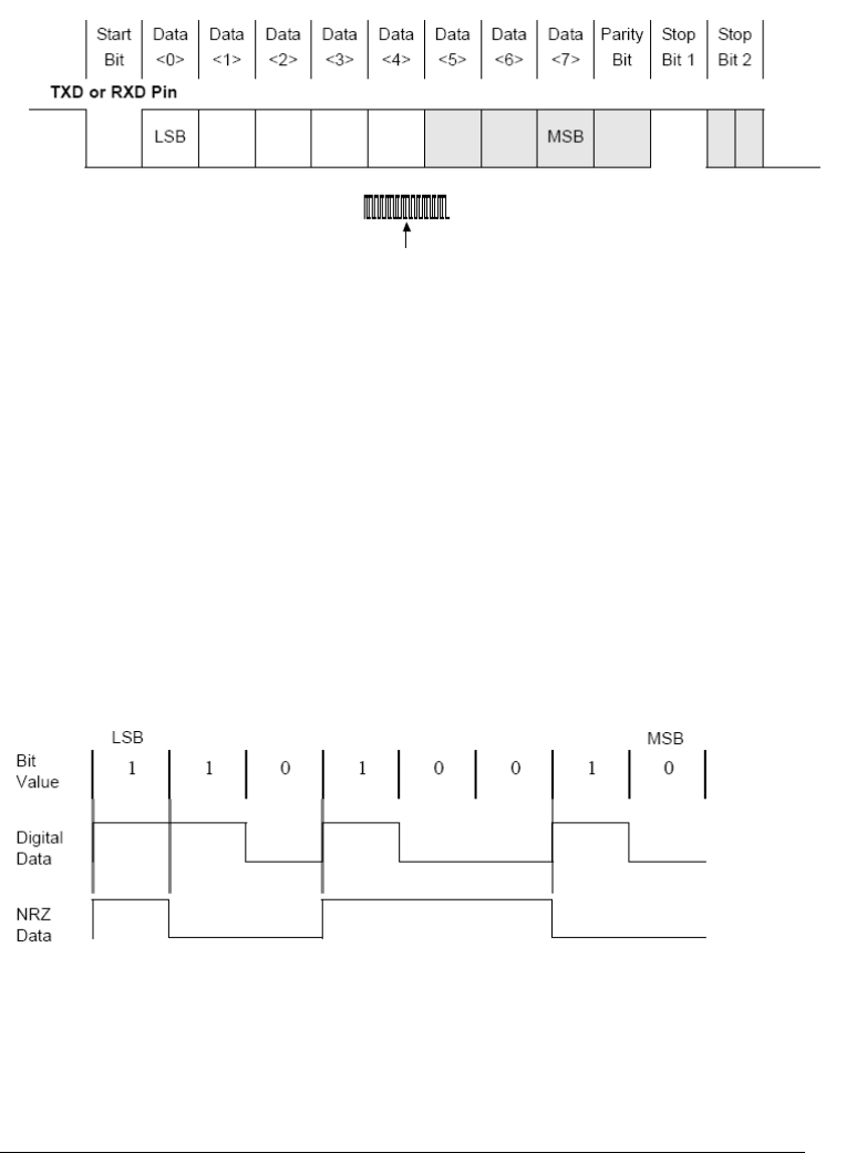
© SENSITECH INC. CONFIDENTIAL – CONTROLLED DOCUMENT
Page 38 of 83
A Carrier Corp. Company
PART NUMBER T82002163
REV A
The receive-data sample counter frequency is 16 times the value of the bit frequency. The 16X
clock is created by the baud-rate generator. Each bit is sampled three times in the middle. Shaded
bits in Figure 10-1 are optional and can be programmed by software.
Each data frame is between 7 and 12 bits long, depending on the size of the data programmed,
whether parity is enabled, and the number of stop bits. A data frame begins by transmitting a start
bit that is represented by a high-to-low transition. The start bit is followed by from 5 to 8 bits of
data that begin with the least significant bit (LSB). The data bits are followed by an optional parity
bit. The parity bit is set if even-parity is enabled and the data byte has an odd number of ones, or if
odd parity is enabled and the data byte has an even number of ones. The data frame ends with 1,
1½, or 2 stop bits, as programmed by software. The stop bits are represented by 1, 1½, or 2
successive bit periods of logic 1.
Each UART has two FIFOs: one transmit and one receive. The transmit FIFO is 64 bytes deep and
8 bits wide. The receive FIFO is 64 bytes deep and 11 bits wide. Three bits are used for tracking
errors.
The UART can use non-return-to-zero (NRZ) coding to represent individual bit values. To enable
NRZ coding, set IER[5]. A bit value of 0b1 is represented by a line transition, and 0b0 is
represented by no line transition. Figure 10-2 shows the data byte 0b0100_1011 in NRZ coding.
The byte’s LSB is transmitted first.
Figure 10-2. Example NRZ Bit Encoding—0b0100_1011
Reset
The UARTs are disabled on reset. To enable a UART, software must program the GPIO registers
(see Section 24, “General-Purpose I/O Controller”), then set IER[UUE]. When the UART is
enabled, the receiver waits for a frame-start bit and the transmitter sends data if it is available in the
Transmit Holding register. Transmit data can be written to the Transmit Holding register before the
UART unit is enabled. In FIFO mode, data is transmitted from the FIFO to the Transmit Holding
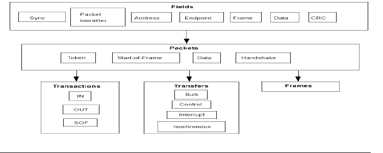
© SENSITECH INC. CONFIDENTIAL – CONTROLLED DOCUMENT
Page 39 of 83
A Carrier Corp. Company
PART NUMBER T82002163
REV A
register before it goes to the pin.
When the UART unit is disabled, the transmitter or receiver finishes the current byte and stops
transmitting or receiving more data. Data in the FIFO is not cleared, and transmission resumes
when the UART is enabled.
USB Client Controller:
Overview
The UDC supports 24 endpoints (endpoint 0 plus 23 programmable endpoints). The UDC is a USB
Revision 1.1-compliant, full-speed device that operates half-duplex at a baud rate of 12 Mbps (as a
slave only, not as a host or hub controller).
The serial information transmitted and received by the USB client controller contains layers of
communications protocols as defined by Universal Serial Bus Specification, Revision 1.1, the most
basic of which are fields.
• USB fields include: sync, packet identifier, address, endpoint, frame number, data, and CRC.
Fields are used to produce packets. Depending on the packet function, a different combination
and number of fields can be used.
• Packet types include: token, start of frame, data, and handshake. Packets are assembled into
groups to produce transfers, transactions, and frames.
• Transfers fall into four groups: bulk, control, interrupt, and isochronous.
• Transactions fall into four groups: IN, OUT, SOF, and SETUP. Data flow is relative to the
USB host controller. IN packets represent data flow from the USB client controller to the host
controller. OUT packets represent data flow from the USB host controller to the client
controller.
Figure 12-1 graphically represents the communications layers in the protocol. See the Universal
Serial Bus Specification, Revision 1.1 for more details on USB protocol.
The UDC uses single-ported memory to support FIFO operations. Bulk, isochronous, and interrupt
endpoint FIFO structures can be double-buffered to enable the endpoint to process one packet
while assembling another. Use either DMA or the Intel XScale® core to fill and empty the FIFOs.
An interrupt, DMA service request, or polling can be used to detect packet receipt.
The USB host controller referenced in this chapter refers to any USB host controller that is
compliant to the Universal Serial Bus Specification, Revision 1.1, including the PXA27x
processor’s internal USB host controller.
Figure 12-1. Communications Protocol Layers in the USB Client Controller
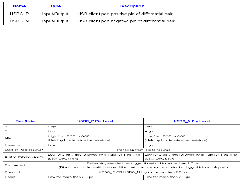
© SENSITECH INC. CONFIDENTIAL – CONTROLLED DOCUMENT
Page 40 of 83
A Carrier Corp. Company
PART NUMBER T82002163
REV A
Features
• USB Revision 1.1, full-speed compliant device
• 23 programmable endpoints
— Type: bulk, isochronous, or interrupt
— Direction: in or out
— Maximum packet size
— Programmable configuration, interface and alternate interface setting numbers
• Endpoint 0 for control IN and OUT
• Four configurations:
— Three programmable configurations with up to seven interfaces with seven alternate
interface settings
— Default configuration 0 with one interface and control endpoint 0
• Configurable 4-Kbyte memory for endpoint data storage
Signal Descriptions
This section describes the signals used by the USB client controller (See Table 12-1).
Table 12-1. USB Client Controller Interface I/O Signal Descriptions
Bidirectional Signals
USBC_P and USBC_N are the differential lines of the USB cable. Using differential signaling
allows transmitting multiple states on the serial bus. These states are combined to transmit data as
well as various bus conditions, including: idle, resume, start-of-packet (SOP), end-of-packet
(EOP), disconnect, connect, and reset. Four distinct states are represented using differential data by
decoding the polarity of the USBC_P and USBC_N pins. Two of the four states are used to
represent data. A one is represented when USBC_P is high and USBC_N is low; a zero is
represented when USBC_P is low and USBC_N is high. The remaining two states and pairings of
the four encodings are decoded further to represent the current state of the USB. Table 12-2 shows
how seven different bus states as well as one and zero are represented using differential signaling.
Table 12-2. USB States Using Differential Signaling
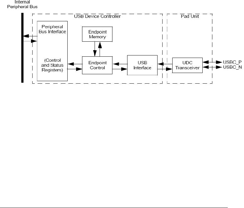
© SENSITECH INC. CONFIDENTIAL – CONTROLLED DOCUMENT
Page 41 of 83
A Carrier Corp. Company
PART NUMBER T82002163
REV A
Operation
The UDC consists of four major components: the peripheral bus interface, endpoint memory,
endpoint control, and USB interface. The peripheral bus interface contains the UDC control and
status registers for the endpoint configuration data and provides the interface between the PXA27x
processor and the USB data. The endpoint memory is a 4-Kbyte SRAM used for USB endpoint
data storage. It has 32 bytes dedicated to endpoint 0, allowing the remainder of its memory to be
allocated to any of the 23 programmable endpoints. The endpoint control and USB interface blocks
provide the USB functionality. Figure 12-2 is a block diagram of the USB client controller and its
dedicated I/O.
Figure 12-2. USB Client Controller Block Diagram
Peripheral Bus Interface and Control/Status Registers
The UDC is a slave peripheral device that is connected to the internal peripheral bus. All userinitiated
accesses to the UDC registers and endpoint memory are completed using the internal
peripheral bus. The control and status registers include registers for frame-number storage, UDC
top-level control and status, interrupt control and status, endpoint control, status, and data transfer.
The UDC Control register (UDCCR) provides control and status of internal UDC functions. The
UDCCR status bits indicate the current USB configuration, interface, and alternate interface setting
numbers assigned the UDC by the USB host controller. The UDCCR also contains a status bit to
indicate if the UDC is actively communicating on the USB, and a status bit to indicate an unusable
endpoint memory configuration. The UDCCR also allows selection of UDC enable for USB
operation, UDC resume, and endpoint memory configuration control
Either processor interrupts or polling can be used to determine whether USB activity occurs. The
Frame Number register (UDCFNR) holds the frame number contained in the last received start-offrame
(SOF) packet.
Although the UDC can generate only a single interrupt to the processor’s interrupt controller, there

© SENSITECH INC. CONFIDENTIAL – CONTROLLED DOCUMENT
Page 42 of 83
A Carrier Corp. Company
PART NUMBER T82002163
REV A
are 53 sources for this interrupt. Each of the 24 endpoints (0 and A–X) has two interrupts: packet
complete and FIFO error. In addition, the UDC has five interrupts that can be generated based on
USB activity. The interrupt sources are shown in the UDC Interrupt Status registers, which must be
read to determine the cause of the interrupt being generated. In addition, USB activity can be
determined by reading the UDC Interrupt Status registers. If polling is used, the Endpoint Control/
Status registers can be read to determine activity on the USB.
The UDC Interrupt Control registers contain interrupt-enable bits that enable the generation of the
UDC interrupt. When an interruptible event occurs, the appropriate status bit in the Endpoint
Control/Status register is set, and if the corresponding interrupt-enable bit in the Interrupt Control
register is set, then the appropriate bit in the Interrupt Status register is set and an interrupt is
generated. An interrupt is cleared by setting the appropriate bit in the Interrupt Status registers
Endpoint 0 is the only control endpoint and the only bidirectional endpoint in the UDC, and has
characteristics different from the programmable endpoints A–X. Key characteristics of endpoint 0
include the following:
• Control/Status, Byte Count, and Data registers
• Configuration is fixed and does not use a configuration register
• Enabled for every USB configuration and interface
• Bidirectional endpoint with 32 bytes of USB data-storage space allocated in the endpoint
memory: 16 bytes of FIFO memory are used for IN data and 16 bytes are used for OUT data
• USB data space is not double-buffered.
• Only endpoint configured and available for USB operation after USB reset, and before the
USB host controller has enumerated the UDC
The Endpoint 0 Control/Status and Byte Count registers provide the status of the endpoint 0 IN and
OUT buffers. The Receive FIFO Not Empty bit (UDCCSR0[RNE]) and OUT Packet Complete bit
(UDCCSR0[OPC]) are set when a complete data packet has been received from the USB host
controller. If the packet is part of a SETUP transaction, the Setup Active bit (UDCCSR0[SA]) is
also set. The endpoint 0 transmit FIFO is flushed by the UDC after receiving an OUT data packet
from the USB host controller. The Byte Count register (UDCBCR0) indicates the number of bytes
of data that need to be unloaded from the receive buffer. As data is read from the endpoint 0 receive
buffer using the Endpoint 0 Data register UDCDR0, the Byte Count register value is decremented
to indicate the number of bytes remaining in the buffer. When all of the data has been unloaded
from the receive buffer, UDCCSR0[RNE] is cleared by the UDC to indicate the receive buffer is
empty. After reading all of the data from the endpoint 0 receive buffer, software must clear
UDCCSR0[OPC] to enable the buffer to receive another USB data packet.
Loading a maximum packet size of 16 bytes into the endpoint 0 transmit FIFO automatically sets
UDCCSR0[IPR]. If less than 16 bytes are loaded into the endpoint 0 transmit FIFO,
UDCCSR0[IPR] must be explicitly set to indicate a complete packet has been loaded. When the
data has been transmitted to the USB host controller, the UDC clears UDCCSR0[IPR] to indicate
the packet has been sent
Each of the 23 programmable endpoints, referred to as endpoints A–X, has a Configuration
register, Control/Status register, Byte Count register, and a Data register. The Configuration
registers set the configuration, interface, alternate setting and endpoint numbers, and maximum
packet size, as well as enable double-buffering for each endpoint. The Configuration registers can
be written only when the UDC is not enabled (UDCCR[UDE] is clear). When UDCCR[UDE] is
set, the endpoint configurations are loaded into the USB interface block and are set to read-only
access.
The Control/Status, Byte Count, and Data registers control the operation of each endpoint after
enumeration. If an endpoint has double-buffering disabled, the Control/Status and Byte Count
registers provide the status of the endpoint buffer. If the endpoint is configured as an OUT

© SENSITECH INC. CONFIDENTIAL – CONTROLLED DOCUMENT
Page 43 of 83
A Carrier Corp. Company
PART NUMBER T82002163
REV A
endpoint, the FIFO Service (FS) and Packet Complete (PC) bits in the Endpoint Control/Status
register are set when a complete data packet has been received from the USB host controller.
The Byte Count register of each endpoint indicates the number of data bytes that need to be
unloaded from the buffer. As data is read from the FIFO memory using the Data register, the
corresponding Byte Count register value is decremented to indicate the number of bytes remaining
in the buffer. When all of the data has been unloaded from the FIFO memory, the FS and Buffer
Not Empty/Buffer Not Full (BNE/BNF) bits in the Control/Status register and the Byte Count (BC)
in the Byte Count register are cleared by the UDC to indicate the current buffer is empty. After
reading all of the data from the endpoint buffer, software must clear the PC bit in the corresponding
Control/Status register.
If an OUT endpoint has double-buffering enabled, the Control/Status and Byte Count registers
provide the status of the endpoint buffer that is currently active. The FS, PC, and BNE/BNF bits in
the Endpoint Control/Status register are set when the first buffer has received a complete data
packet. The short-packet (SP) bit indicates a packet smaller than the maximum packet size has been
received and is ready for unloading, or has been loaded and is ready for transmission. The Data
register unloads data from the first buffer. The Control/Status and Byte Count registers continue to
hold the status of the first buffer until software clears the PC bit in the Control/Status register.
As the data is read from the first receive buffer, the value in the Byte Count register is decremented
and indicates the number of data bytes that still need to be read from the first buffer in the FIFO
memory. When all of the data in the first buffer has been read, the Byte Count register and the
BNE/BNF bit in the Control/Status register are cleared. If a second packet is received before all of
the data has been read from the first buffer, the FS bit continues to be set after the first buffer is
been read, but the second packet of data does not set the PC bit until after software has cleared the
PC bit.
The status of the second buffer cannot be determined until the PC bit is cleared. The PC bit must be
set to update the Control/Status and Byte Count registers with the status of the second buffer. If the
PC bit is set before reading all of the data in the first receive buffer, the data in the first receive
buffer is lost.
If the second buffer has received a complete data packet, the PC bit is again set to indicate that the
endpoint FIFO has data ready to be unloaded, and the BNE/BNF and Byte Count registers indicate
the amount of data present in the second buffer. At this point, the Data register unloads data from
the second buffer. The Control/Status and Byte Count registers continue to hold the status of the
second buffer until software again clears the PC bit. Only after all of the data has been read from
the second buffer must the PC bit be set. Doing so updates the Control/Status and Byte Count
registers to reflect the status of the first buffer.
Suspend and Resume
If idle persists on the USB for more than 3 ms, the UDC detects the suspend state, and (if the
suspend interrupt is enabled) an interrupt is sent to the processor. When the UDC enters the
suspend state, the processor stops the 48-MHz clock to the UDC and enables the UDC pins
USBC_P and USBC_N to detect the resume state. If the processor does not enter sleep mode, the
state of the UDC is preserved and is ready for resume detection.
Note: The presence of SOF packets prevents the UDC from entering suspend mode.
The UDC can exit suspend in three ways:
• Resume initiated by the UDC
• Resume initiated by the USB host controller
• USB reset
If the USB host controller has executed the SET_FEATURE command and enabled the device

© SENSITECH INC. CONFIDENTIAL – CONTROLLED DOCUMENT
Page 44 of 83
A Carrier Corp. Company
PART NUMBER T82002163
REV A
remote wake-up feature of the UDC, after the UDC has entered the suspend state, sending a wakeup
signal to the USB host controller is performed by setting UDCCR[UDR]. Doing so forces the
UDC to drive a non-idle state (K state) onto the USB for 3 milliseconds without further user
intervention. The UDC hardware then clears UDCCR[UDR]. The UDC waits for the resume signal
to be reflected back to it by the USB host controller, and when the resume state is detected on the
USB, if the resume interrupt is enabled, an interrupt is sent to the processor.
The USB host controller can wake up the UDC by driving the non-idle state (K state) either by
driving a resume or USB reset onto the USB. When the UDC pads detect this non-idle state on the
USB, they signal the processor clock manager module to start the 48-MHz clock to the UDC, and
(if the resume interrupt is enabled) an interrupt is sent to the processor. Software must take the
appropriate action to resume activity.
Sleep Mode Operation
If the UDC has entered the suspend state before the PXA27x processor is in sleep mode, the UDC
pins USBC_P and USBC_N are used to detect the resume state on the USB and resume operation
while the processor is in sleep mode. If the USB host controller tries to access the UDC when the
processor is in sleep mode, the USBC_P and USBC_N pins detect the resume state and signal the
processor to begin the wake-up sequence. The UDC will have lost all state information and the
UDC Configuration registers must be reloaded prior to setting UDCCR[UDE]. The USB host
controller must issue a USB reset and re-enumerate the UDC.
If the UDC has been disconnected from the USB and the processor is in sleep mode, a GPIO pin
must be programmed to detect connection to the USB and to signal the processor to begin the
wake-up sequence. The GPIO pin must be connected through a level-shifter to the USB power
signal to detect connect/disconnect to the USB. The UDC will have lost all state information and
users must load the UDC Configuration register and enable the UDC before the UDC is ready for
USB operation.
USB On-The-Go Operation
The processor USB device and host controllers can be used to provide A- and B-device On-The-Go
(OTG) operation as specified in the On-The-Go Supplement to the USB 2.0 Specification. The onchip
OTG transceivers provide on-chip pull-up and pull-down resistors as specified in the Pull-up/
Pull-down Engineering Change Notice to the USB 2.0 Specification. OTG operation requires user
intervention but interrupts are provided to notify the user of OTG activities including Vbus
changes, session detection, and OTG ID changes. The user must use these interrupts along with the
OTG control and status registers to operate as an OTG device. The UDC OTG support includes the
following:
• Decoding of SET_FEATURE commands with OTG specific selector values
• Control for on-chip OTG transceiver with multiplexing between UDC and USB host controller
(UHC) port 2
• Control for multiplexing between UDC, UHC port 2 and UHC port 3 data through GPIOs
• Control, status and interrupt registers for interfacing to off-chip OTG transceivers
• Control, status and interrupt registers for interfacing to off-chip charge pump devices
• OTG ID support
Figure 12-15 shows each of the configurations provided to support OTG operation. Each of these is
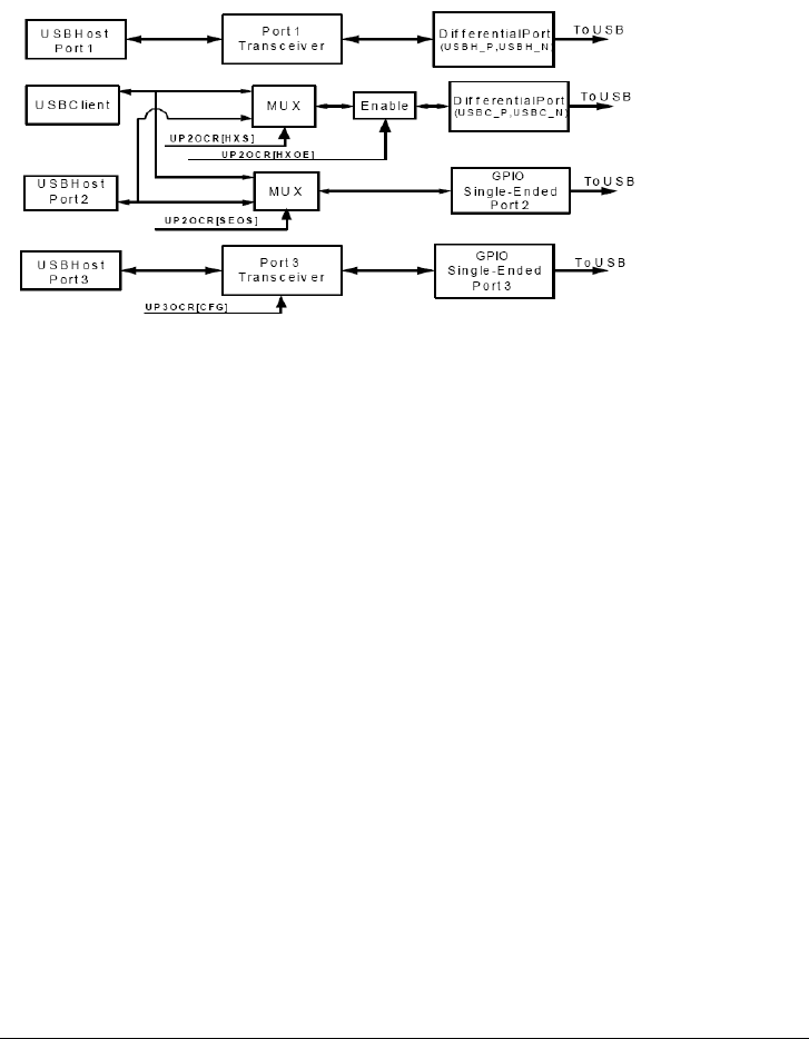
© SENSITECH INC. CONFIDENTIAL – CONTROLLED DOCUMENT
Page 45 of 83
A Carrier Corp. Company
PART NUMBER T82002163
REV A
discussed in detail.
Note: The processor does not provide direct connection to or control of the USB Vbus.
Figure 12-15. USB OTG Configurations
On-Chip OTG Transceiver Operation
The USB host port 2 transceiver is designed in accordance with the Pull-up/Pull-down Resistors
Engineering Change Notice to the USB 2.0 Specification to provide on-chip resistors and OTGcompliant
transceiver operation. The USB host controller port 2 multiplexor is a bidirectional I/O
multiplexor that connects to the USB host port 2 transceiver and the single-ended I/O through the
GPIO. The port 2 multiplexor provides an interface that allows the UDC port or UHC port 2 to
connect to the UHC port 2 transceiver for direct bidirectional connection to the USB. The port 2
multiplexor also provides an interface that allows the UDC port, UHC port 2, and the UHC port 3
to connect to single-ended I/O through the GPIOs.
The OTG transceiver contains two pull-up resistors and one pull-down resistor on each D+ and D–
that can be enabled using the USB Port 2 Output Control Register (UP2OCR) pull-up/pull-down
enable bits (DPPUBE, DMPUBE, DPPUE, DMPUE, DPPDE, DMPDE). Figure 12-16 illustrates
the on-chip host port 2 transceiver pad with the pull-up and pull-down resistors.
• Enable SW3 for both D+ and D– when host port 2 is being used for USB host controller data.
• Enable SW1 on the D+ pad and disable SW1 on the D– pad when host port 2 is being used for
USB device controller data.
• Disable SW2 on the D+ and D– pads when host port 2 is being used for USB device controller
data.
• SW2 is enabled and disabled by hardware when the UDC is idle and receiving data from an
upstream device as specified in the Pull-up/Pull-down Resistors Engineering Change Notice
to the USB 2.0 Specification. Table 12-9 lists the switch settings used for the USB host and
USB device controller I/O.
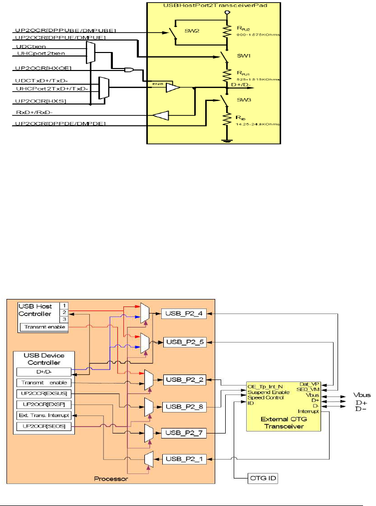
© SENSITECH INC. CONFIDENTIAL – CONTROLLED DOCUMENT
Page 46 of 83
A Carrier Corp. Company
PART NUMBER T82002163
REV A
Figure 12-16. Host Port 2 OTG Transceiver
Interface to External OTG Transceiver
In the case where the user does not use the internal OTG transceiver, the UDC contains control,
status, and interrupt registers to provide seamless interfacing to external transceivers. External
transceivers can be used to provide D+, D–, and Vbus driver to the USB. In this mode, the USB D+
and D– signals are output through GPIO pads with UP2OCR[SEOS] used to control multiplexors
to select between UDC and USB host controller D+, D–, and transmit enable signals. In addition,
the USB Port 2 Output Control Register (UP2OCR) provides the external transceiver suspend
(EXSUS) and external transceiver speed (EXSP) control output bits, and the external transceiver
interrupt input to interface to the external transceiver. Figure 12-17 illustrates the OTG connection
to an external transceiver.
Figure 12-17. Connection to External OTG Transceiver
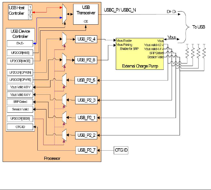
© SENSITECH INC. CONFIDENTIAL – CONTROLLED DOCUMENT
Page 47 of 83
A Carrier Corp. Company
PART NUMBER T82002163
REV A
Note: For Figure 12-17, UP2OCR[SEOS] = 4 for USB client and UP2OCR[SEOS] = 5 for USB host.
Interface to External Charge Pump Device
In addition to the interface options described in Section 12.5.4, the UDC provides control outputs
and interrupt inputs to drive and monitor an external charge pump device. To do so, the USB D+
and D– signals can be output using the on-chip OTG transceiver and the Vbus interface provided
by an external charge pump device. In this mode, UP2OCR[HXS] is used control multiplexors to
select between UDC and USB host controller D+, D–, and transmit enable signals to be output
through the USB host controller port 2 transceiver. In addition, USB Port 2 Output Control
Register (UP2OCR) provides the charge pump Vbus enable (CPVEN) and charge pump Vbus
pulse enable (CPVPE) control output bits used to enable the driving of Vbus and to enable the
driving of pulses on Vbus, respectively. Additionally, USB Port 2 Output Control Register
(UP2OCR) provides the Vbus valid 4.0-V, Vbus valid 4.4-V, session valid, and session request
protocol detected interrupt inputs to interface to the external charge pump device. Figure 12-18
illustrates the OTG connections to an external charge pump device.
Figure 12-18. Connection to External OTG Charge Pump
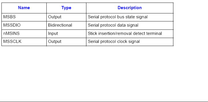
© SENSITECH INC. CONFIDENTIAL – CONTROLLED DOCUMENT
Page 48 of 83
A Carrier Corp. Company
PART NUMBER T82002163
REV A
Memory Stick
Overview
The Memory Stick is a medium for storing and transferring data. In its simplest form, the Memory
Stick is a small, pluggable card containing flash (or other similar) memory. This memory can store
multiple content types—for example, audio data or stored image data. In addition to this basic
form, other devices are available that use the standard Memory Stick definition (for example,
camera modules). The memory stick host controller provides the interface between the PXA27x
processor and one Memory Stick.
Note: The Sony Memory Stick Standard, Format Specification Version 1.3 (the Sony MS standard)
defines the Memory Stick interface and provides the basis for this chapter. For all details of
Memory Stick operation, refer to this Sony standard.
Features
•
Compliance with the Sony Memory Stick standard
•
Built-in transmit and receive FIFO buffers
•
Built-in CRC calculation and checking
•
Transfer clock up to 20 MHz
•
Data transfer using programmed I/O, interrupt to processor, and DMA
•
Automatic command execution when an interrupt from the Memory Stick is detected
Signal Descriptions
Table 17-1 summarizes the signals used by the memory stick host controller.
Operation
The memory stick host controller communicates with the Memory Stick using a half-duplex serial
protocol. This section presents an overview of the protocol. Always refer to the Sony MS standard
for details.
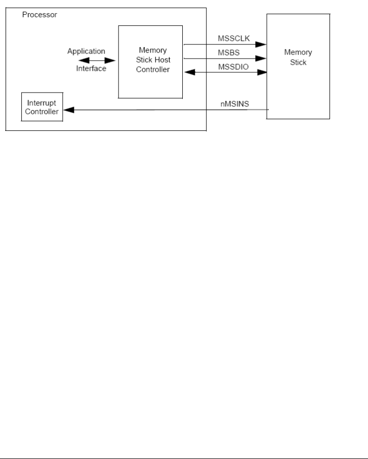
© SENSITECH INC. CONFIDENTIAL – CONTROLLED DOCUMENT
Page 49 of 83
A Carrier Corp. Company
PART NUMBER T82002163
REV A
Functional Description
The Memory Stick system, depicted in Figure 17-1, consists of the memory stick host controller
and an attached Memory Stick card.
Figure 17-1. Memory Stick System Block Diagram
The memory stick host controller interfaces with the Memory Stick using a 32-bit internal
application interface. It allows:
•
Sending of transfer protocol commands (TPCs) to the Memory Stick using the MSHC
Command register.
•
Data transfer using the two separate receive (RX) and transmit (TX) FIFOs (this data can be
transferred using polling, interrupts to the processor, or DMA).
•
Responding directly to Memory Stick interrupts by issuing a predefined command, the
AutoCommand (ACD).
•
Placing the card into a low-power mode.
Interrupts
The memory stick host controller generates a single interrupt to the interrupt controller. The cause
of the interrupt can be determined by reading the Interrupt and Status register.
Status bits in this register indicate which event caused the interrupt to be generated. Interrupts can
be disabled (either individually or in total) by setting bits in the Interrupt Enable register.
To process an interrupt, MSINTEN[INTEN] must be set, and the enable bit for the specific
interrupt in register MSINTEN must be set.
It is possible for multiple secondary interrupts to occur if more than one MSINTEN register bit
besides INTEN are set. To determine the specific cause of the interrupt, read the Interrupt and
Status register, MSINT. To handle more than one interrupt at a time, set MSINTEN[INTEN] and
the specific MSINTEN interrupt enable bits.
Memory Stick Insertion and Removal
The nMSINS signal indicates the insertion and removal of a Memory Stick. nMSINS is connected
to the interrupt controller, but not to the memory stick host controller. Thus, the interrupt controller
must be programmed to generate an nMSINS interrupt.
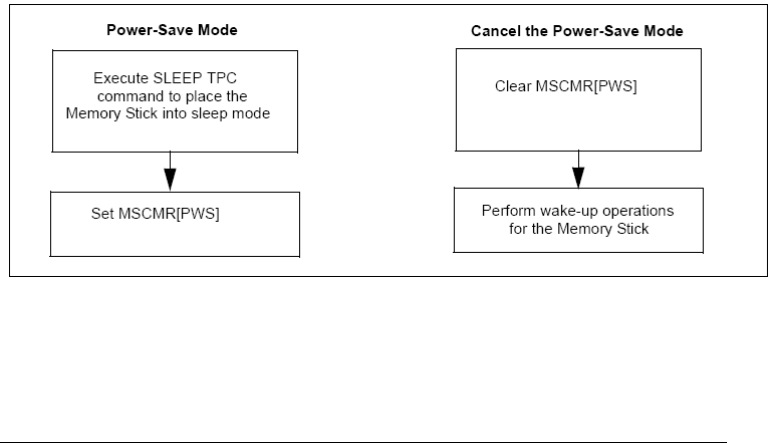
© SENSITECH INC. CONFIDENTIAL – CONTROLLED DOCUMENT
Page 50 of 83
A Carrier Corp. Company
PART NUMBER T82002163
REV A
Software must monitor the nMSINS interrupt. When an interrupt occurs due to the removal of the
memory stick, the software must halt all MHSC activity and reset the memory stick host controller.
Reset
The memory stick host controller is reset in either of two ways:
•
Any PXA27x processor reset causes all of the MSHC registers to be reset.
•
Setting MSCRSR[RST] causes the memory stick host controller to enter and remain in reset
until MSCRSR[RST] is cleared. In this case, all of the registers except for the RST bit are
reset, and the output signals BS, SDIO, and SCLK are driven low. Any currently-executing
protocol is terminated when MSCRSR[RST] is asserted.
These methods do not cause a reset TPC to be sent to the Memory Stick.
Note: Before writing any of the control registers for a new bus protocol, always set MSCRSR[RST] and
then clear it.
Power-Save Mode
When the memory stick is not being used, software may optionally place it into a low-power mode.
This is controlled entirely by software and is not related in any way to the PXA27x processor lowpower
modes.
Figure 17-2 shows how to enter and exit the Memory Stick power-save mode. To maximize overall
system power saving, software must place the Memory Stick in power-save mode prior to entering
any of the system low-power modes.
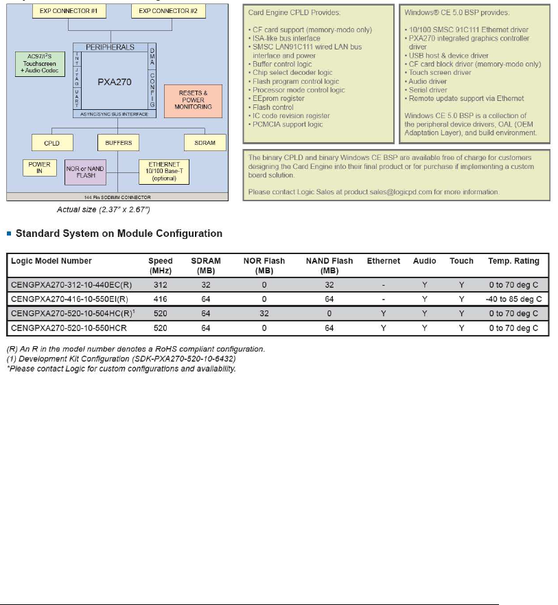
© SENSITECH INC. CONFIDENTIAL – CONTROLLED DOCUMENT
Page 51 of 83
A Carrier Corp. Company
PART NUMBER T82002163
REV A
LogicPD Card Engine:
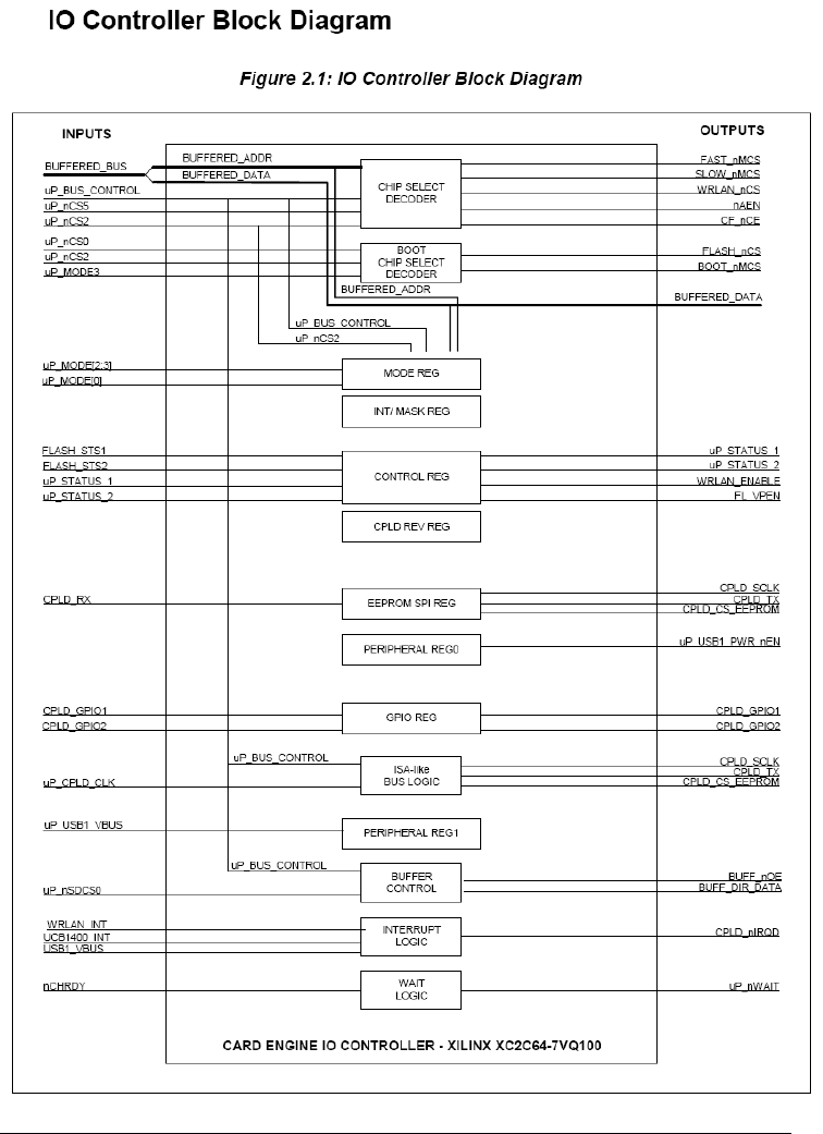
© SENSITECH INC. CONFIDENTIAL – CONTROLLED DOCUMENT
Page 52 of 83
A Carrier Corp. Company
PART NUMBER T82002163
REV A
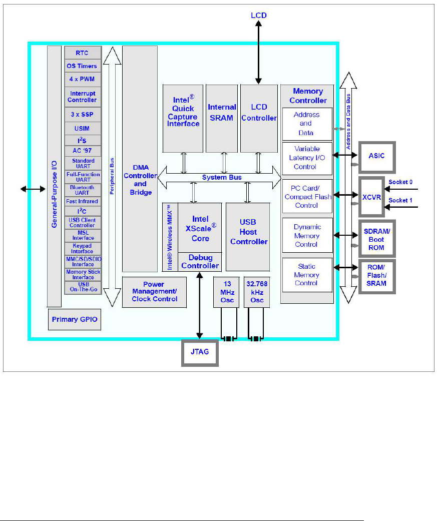
© SENSITECH INC. CONFIDENTIAL – CONTROLLED DOCUMENT
Page 53 of 83
A Carrier Corp. Company
PART NUMBER T82002163
REV A
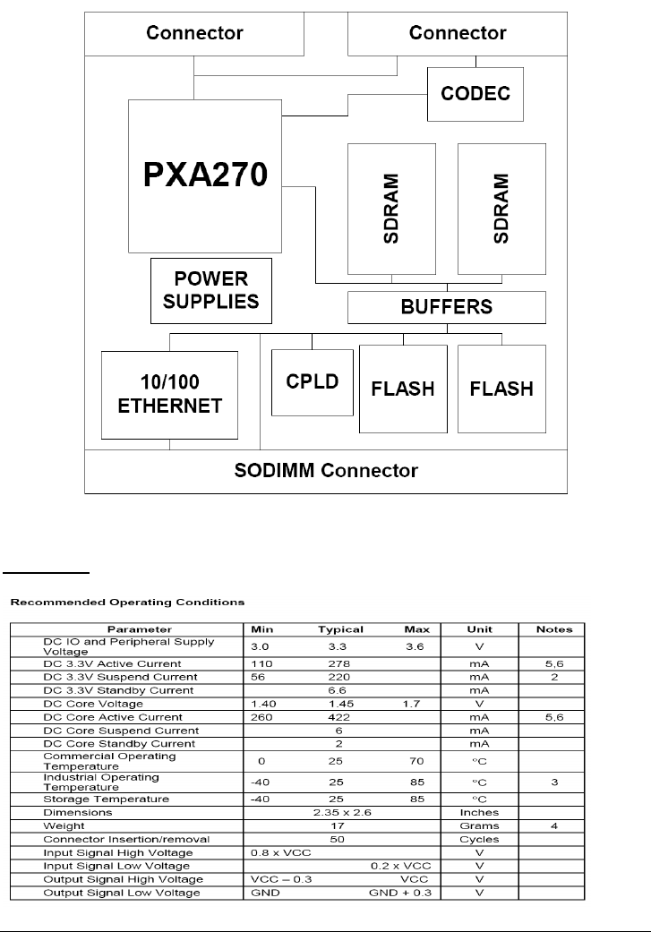
© SENSITECH INC. CONFIDENTIAL – CONTROLLED DOCUMENT
Page 54 of 83
A Carrier Corp. Company
PART NUMBER T82002163
REV A
Note: Our current Card Engine does support Ethernet.
Card Engine:
© SENSITECH INC. CONFIDENTIAL – CONTROLLED DOCUMENT
Page 55 of 83
A Carrier Corp. Company
PART NUMBER T82002163
REV A
TempTale Mini
During normal monitor operation, communications mode is disabled. In order to enable the
communications mode by means of the communications enable pin on the RS232 connector located
inside the monitor. This pin must be held during the entire communications session. The monitor
communicates via a standard RS232, 9600 baud rate, 8 bit, No Parity, 2 Stop bit protocol. (9600,8,N,2)
Once the monitor has entered communications mode, the host PC is responsible for establishing a
connection with the monitor. If the host PC does not establish a connection within one minute’s time,
the microcontroller within the monitor will disable communications mode thus terminating
communications. If this occurs, it will be necessary to re-enable the communications mode by re-
triggering the communications enable line.
To establish a connection with the monitor, the host PC must send a sequence of
Bytes to the monitor and receive the correct responses back from the monitor. This sequence is designed to
give the monitor time to wake-up and allow the host to log in. If any of the bytes are sent or received
incorrectly or at the wrong time during the connection attempt, both the host and monitor should
assume bad communications and return to their previous states. The following table shows the steps
that are taken to connect to the monitor:
Table 1
Step
# Host PC’s Action Monitor’s
Action Action Description
1 Toggle
Communications
Enable Line
(DTR)
Detect Com Line
toggle and enter in
Comm. Mode
Wake-up Monitor via RS232 line toggle
2 Send 00h
Rcv 00h and
Send Product ID of
02h to host
Host send 00h
Monitor replies by sending 2 byte Product
ID of 02h, low byte 02h, high byte 00h,
LSB first
3 Rcv ID and set-up for
correct protocol
Send Next Command
Rcv command
from host and act
accordingly
Host determines monitor type via ID value
and sends next action command.
As can be seen in Table 2 above, the first thing to happen is the monitor enters communications mode via a
change in state in the “detect” line from the RS232 connector. (“Detect” = Pin 4 (DTE Ready) of the
DB9 connector)
The host PC initiates communications by transmitting a 1-byte hex value of 0h to the monitor.
When the monitor is able to respond, it will reply by transmitting a 2-byte (16 bit) protocol ID hex value of
2h back to the host computer. It does this by sending the low byte first and the high byte second.
The host PC then looks at the value that it got back for the protocol ID and determines what command
protocol to use for communicating with the monitor.
Once the host PC has successfully logged in and has established a connection with the monitor. The host
PC may now send predefined commands to the monitor, which allows it to do things such as, configure
the monitor or download the data. The command protocol and a list of the commands with their
definitions are described in a later section. It is also important to note that once a connection has been
established, a 3-minute timeout timer is established within the monitor in place of the 1-minute timeout
© SENSITECH INC. CONFIDENTIAL – CONTROLLED DOCUMENT
Page 56 of 83
A Carrier Corp. Company
PART NUMBER T82002163
REV A
timer. This timer is used as a count down timer that determines the timeout period for communications
between the monitor and host PC. Effectively what this means is that as long as this timer is refreshed
and not allowed to expire, communications mode will stay active allowing commands to be sent. The
monitor refreshes this timer any time valid command is sent, so as long as commands continue to be
sent, the monitor will continue to refresh the timer. If no commands are sent to the monitor within 3
minutes, communications mode within the monitor will be terminated. The reason for the 3-minute
timeout timer is to maximize the battery life of the monitor. Because of the power drain associated
with the communications mode, if the communications mode were allowed to continue indefinitely,
the battery would be drained very quickly.
Once the parameters or the 0h have been received, the monitor will then internally execute the command
and return a status byte followed by any additional data.
A status byte is always returned from the monitor upon completing a command whether or not there is any
additional data. The status byte is always a single byte value. A 0h value indicates successful
completion of the command while a non-zero value indicates an error. A list of valid status codes with
their names and descriptions are in the table below:
Status name Code Description
CMD_SUCCESSFUL 0x00 Returned upon successful completion of command.
CMD_UNKNOWN 0x02 The requested command is not part of the unit's API. This is returned
when a command does not exist.
PARAMETER ERROR 0x03 Parameter errors which are sent from the PC
BAD_TEMP 0x04 When an immediate temperature is requested, this value will be returned if
the conversion process did not complete successfully.
RESERVED (UNUSED) 0x05
BAD_INIT 0x07 The unit can not be initialized due to erroneous information having been
stored in its configuration pages.
UNIT_NEW 0x0A The unit is newly manufactured and un-configured.
UNIT_SLEEPING 0x0B The unit is sleeping prior to activation.
UNIT_SDELAY 0x0C The unit has been activated and is waiting through the startup delay.
UNIT_RUNNING 0x0D The unit has completed the startup delay and is actively recording data.
UNIT_STOPPED 0x0E The unit has been stopped after running.
Depending on the command that was sent, the monitor may or may not send data after the status code. For
instance, if the high-speed download command is sent to the monitor, the monitor will send all of the
temperature data after the status code has been sent.
The ULCM also supports a packet based command protocol which uses the same basic structure as the
ULCM standard commands with the exception that the command parameters and return data are in
packet form with a checksum attached. If the command has parameters then the host sends the
command parameter packet just after the monitor echoes back the command value. If the command
returns any data, then the monitor will return the data packet just after the status is sent. The
following figure illustrates this:
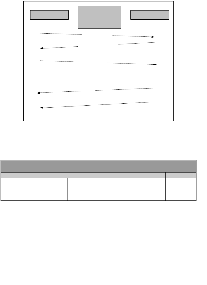
© SENSITECH INC. CONFIDENTIAL – CONTROLLED DOCUMENT
Page 57 of 83
A Carrier Corp. Company
PART NUMBER T82002163
REV A
Figure 1
Executes Command
Command
Echo back command
0x00 or
Parameter Packet
Status
HOST PC MONITOR
ULCM PACKET
COMMAND
PROTOCOL
Data Packet
Note: All data packets will consist of a 3 byte checksum position followed by
the requested data ending with a Checksum
The command parameter packet and data packet use the same packet format, which is shown
below:
Packet Data Checksum
3 byte count of the number of
parameters or data bytes to
follow Parameter or Data bytes
B0 B1 B2 D0, D1, D2, D3, ……….Dn 1Byte
For instance if a ULCM command to download all the data is sent to the monitor, the monitor will send
(after the status byte) a packet containing a 3-byte value representing the number of data bytes to
follow, the data (which includes summary information and temperature data), and a checksum.
For any packet, the checksum is the least significant byte of the sum of all the data in the packet including
the 3-byte checksum position. This is shown in the example below:
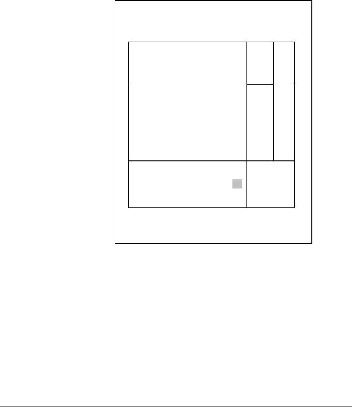
© SENSITECH INC. CONFIDENTIAL – CONTROLLED DOCUMENT
Page 58 of 83
A Carrier Corp. Company
PART NUMBER T82002163
REV A
If the packet contains 1120 data bytes and the value of
all the bytes is a hex 76 then the sum of the count bytes
and data bytes is as follows:
Count Byte 0 0x60
Count Byte 1
0x04
Count Byte 2 0x00
460
H
(112
0D)
Data Byte 0 0x76
Data Byte 1
0x76
Data Byte 2
0x76
.
.
.
.
.
.
Data Byte 1119
0x76
Data Byte 1120 0x76
D
at
a
P
a
c
k
e
t
D
a
t
a
Sum equals 0x208A0 Sum
Once the sum has been calculated, only the least
significant byte, in this case 0xA0, is used as the
checksum.
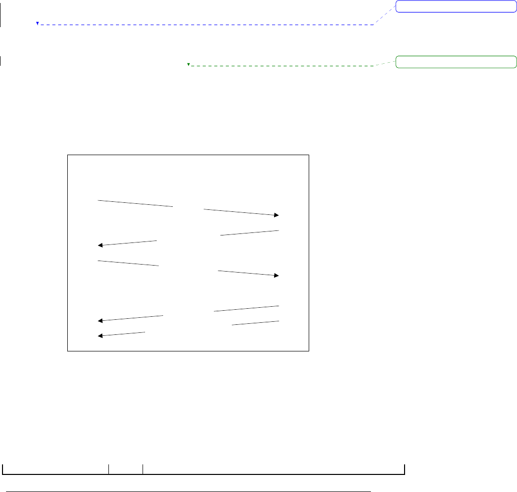
© SENSITECH INC. CONFIDENTIAL – CONTROLLED DOCUMENT
Page 59 of 83
A Carrier Corp. Company
PART NUMBER T82002163
REV A
TempTale 4 (Epson TT4)
Command Transmission Paradigm
As a method of ensuring data integrity, the unit will always echo commands back to the host
computer as it receives them. In this way the external device will know that the unit received a
specific command correctly. This method allows the host computer to respond in the fastest way.
If the unit echoes back the wrong command, the host computer merely disables communications,
thereby forcing the unit to timeout while waiting for a go signal.
If the command is to be followed by a series of data bytes, such as when the host computer is
writing to the Scratchpad, that data is sent by the host computer upon receiving the echoed back
command. Otherwise a 0 is sent by the host to act as a go command. The unit will then perform
the requested action and return an action status byte. Any data or information as required by the
requested action will follow this byte.
command
External
Device TempTale
echo back command
0x00 or parameters
execute
command
command status
any additional response data
Status Byte Definitions
A status byte is always returned from the unit upon completing a command. This is a single byte
value. A '0' value indicates successful completion while a non-'0' indicates an error code. Certain
commands require the unit to be in a specific operating mode. If that condition is not satisfied, the
present mode is sent back as an error code. Status bytes are listed in the table below.
Status name Code Description
CMD_SUCCESSFUL 0x00 Returned upon successful completion of command.
Deleted:
RS232
Deleted:
© SENSITECH INC. CONFIDENTIAL – CONTROLLED DOCUMENT
Page 60 of 83
A Carrier Corp. Company
PART NUMBER T82002163
REV A
CMD_UNKNOWN 0x02 The requested command is not part of the unit's API. This is returned
when a command does not exist. This error code is also returned if a
command that is sent requires a higher access level than the user is
presently in.
BAD_PASSWORD 0x03 During the course of logging into the unit, the supplied password is
incorrect.
BAD_TEMP 0x04 When an immediate temperature is requested, this value will be returned if
the conversion process did not complete successfully.
IIC_TIMEOUT 0x05 During the course of accessing the internally paged memory, either a read
or write time out occurred.
BAD_INIT 0x07 The unit can not be initialized due to erroneous information having been
stored in its configuration pages.
UNIT_NEW 0x0A The unit is newly manufactured and un-configured.
UNIT_SLEEPING 0x0B The unit is sleeping prior to activation.
UNIT_SDELAY 0x0C The unit has been activated and is waiting through the startup delay.
UNIT_RUNNING 0x0D The unit has completed the startup delay and is actively recording data.
UNIT_STOPPED 0x0E The unit has been stopped after running.
Communication Layer Descriptions
The unit utilizes a layered communications protocol. The default layer is no-communications or
Data Recorder mode (unit recording temperature data). The host computer moves from layer 0 to
layer 1 and succeeding layers by successfully sending the appropriate command or sequence of
commands. Presently there are a total of 5 layers. The following table lists the layers by name
and description.
Layer # Layer Name Layer Description
0 Data Recorder No communications - Awaiting communication
initialization sequence.
1 Identification/
Networking Communications Established – Awaiting unit
identification/networking commands.
2 Login/Status Unit Identified - networking issues handled - awaiting
user login.
3 Customer Login
(password
disabled.)
Logged in Customer privilege - all general user
commands available.
4 Sensitech login
(password req.) Logged in with Sensitech privilege. All unit commands
available including test and general commands.
Data Recording Layer
There is no way of telling what the unit may be doing when the host computer tries to initiate
communications. It may be recording data in which case communications are disabled. It may be
in sleep mode, in which case waking up can take 500 milliseconds. One last issue that the unit has

© SENSITECH INC. CONFIDENTIAL – CONTROLLED DOCUMENT
Page 61 of 83
A Carrier Corp. Company
PART NUMBER T82002163
REV A
to deal with erroneous communication attempts. Movement from layer 0 to layer 1 is designed to
eliminate these issues.
Communication is initiated by transmitting a startup sequence of bytes to the unit. This sequence
is designed to give the unit time to wake-up, respond, and synchronize to the host computer’s baud
rate. Unless all steps are performed correctly, the unit will assume bad communications and return
to what it was doing. The bytes transmitted are as follows.
The host computer initiates communications by transmitting a 0x00 to the unit. When the unit is
able to respond to the attempt it will reply by transmitting a 0x00 back to the host computer. At
this point the baud rate has not been established and the computer will receive back garbage.
Possibly more than one byte. Even though the computer will probably not receive a 0x00, any
returned value(s) should be accepted as an indication to continue.
The unit having sent the 0x00, then sets up to receive a 0x55 hex value from the host computer.
The host computer having received the acknowledging 0x00 (or the best approximation thereof)
will have ≈500msec to transmit the next byte in the sequence before the unit terminates the
communications attempt. The host then transmits a 0x55. The unit will use this pattern of 0’s and
1’s to lock onto the host computer’s baud rate. If any other value is received the unit will
terminate communications and return to what it was doing previously. Communications will then
be disabled until the next temperature is taken. This prevents the unit from constantly responding
to a bad communications attempt.
Having received the 0x55 correctly the unit will respond by again transmitting a 0x00 back to the
host. This time the baud rate is correct and the host computer should correctly receive the 0x00.
The host uses this received 0x00 as an indication to transmit the final 4-byte sequence. Again the
host must transmit the final 4 bytes in less than ≈1.0 second or the unit will terminate what it
thinks is a bad communications attempt. The final sequence of 4 bytes is 0x7A, 0x5E, 0x8A, and
0xA1. This last action accomplishes two goals. It verifies that the unit has indeed locked onto to
the correct baud rate and it acts as a simple password against a bogus communications attempt. If
the unit does not receive the correct 4-byte sequence either due to bad communications or
improper baud rate, it will again end communications and return to what it was doing previously.
The unit having received the final four-byte sequence correctly responds by transmitting a 0x00
for a third and final time to the host. The unit is now set to the Network/Identification or layer 1
communications.
The table below shows the sequence of events required to initiate communications with the unit.
Computer Action Unit Response Action Description
xmit 0x00 Reply 0x00 Get unit’s attention
Rcv something - signal to xmit next byte within .5 seconds
xmit 0x55 Reply 0x00 Unit establishes baud rate and responds
rcv 0x00 signal to xmit final 4 byte sequence within 1 second
xmit 0x7A - Sanity check on baud rate detection
xmit 0x5E -
xmit 0x8A -
xmit 0xA1 Reply 0x00 Sanity check successful – respond
rcv 0x00 -
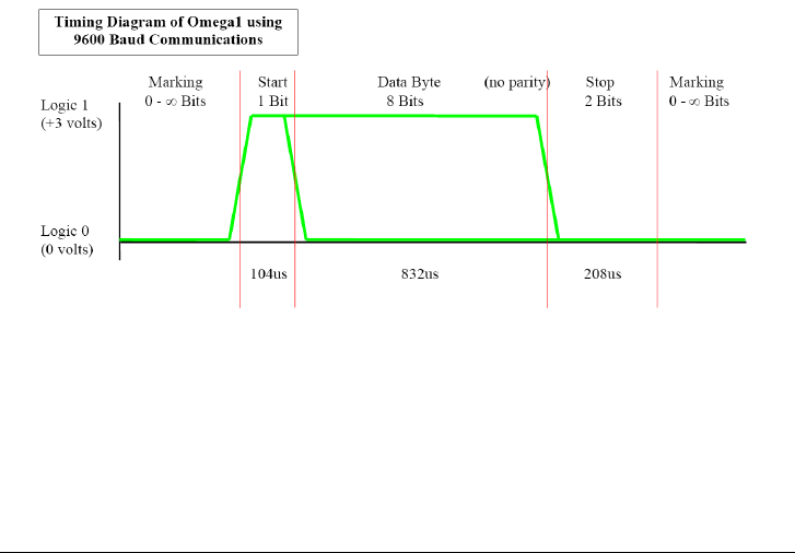
© SENSITECH INC. CONFIDENTIAL – CONTROLLED DOCUMENT
Page 62 of 83
A Carrier Corp. Company
PART NUMBER T82002163
REV A
TempTale 4 (OKI TT4)
Communications
The Monitor has an Infrared optical interface as its primary means for communication to
the outside world. There are also provisions made on the PCB for a hard-wired
asynchronous 0 to +3 volt logic level output. On the optical port, an infrared
phototransistor is used to sense data being input to the device and an infrared LED is
used to transmit data out of the device. This interface will be used for communicating
between an external device (PC w/Interface Plus and TripStrip) and the Monitor. The
hard-wired connection is currently not used but is available for future peripherals.
Any peripheral device that plans to use this connection will be responsible for any
added circuitry that may be required such as voltage level translation, static
protection, drivers, etc. It will also be the peripheral devices responsibility to supply
any power that is needed to operate the added circuitry.
On both interfaces, the data will be transmitted asynchronously using standard RS232
serial protocol. This allows the monitor to connect to a standard RS232 serial port
with very little effort. The monitor UART is setup to receive/transmit data at 9600
Baud with 8 data bits, no parity bit and two stop bits. This can be seen in the diagram
below.

© SENSITECH INC. CONFIDENTIAL – CONTROLLED DOCUMENT
Page 63 of 83
A Carrier Corp. Company
PART NUMBER T82002163
REV A
Establishing a Connection
During normal monitor operation, communications mode is disabled. There are two
ways to enable the monitor’s communications mode. The first method is for an
external device to trigger the monitor’s internal reed switch by means of a magnet. If
this approach is used, the magnet must keep the reed switch triggered during the
entire communications session. The second method is to enable the communications
mode by means of the communications enable pin on the J2 connector located inside
the monitor. This pin must be pulled to ground and held there during the entire
communications session.
Once the monitor has entered communications mode, the host PC is responsible for
establishing a connection with the monitor. If the host PC does not establish a
connection within one minute’s time, the microcontroller within the monitor will
disable communications mode thus terminating communications. If this occurs, it
will be necessary to re-enable the communications mode by either re-triggering the
reed switch by removing it from the magnet for approximately 500msec and then
placing it back near the magnet or by pulling the communications enable pin high for
approximately 500msec and then back to ground.
To establish a connection with the monitor, the host PC must send a sequence of
Bytes to the monitor and receive the correct responses back from the monitor. This
sequence is designed to give the monitor time to wake-up and allow the host to log in.
If any of the bytes are sent or received incorrectly or at the wrong time during the
connection attempt, both the host and monitor should assume bad communications
and return to their previous states. The following table shows the steps that are taken
to connect to the monitor:
© SENSITECH INC. CONFIDENTIAL – CONTROLLED DOCUMENT
Page 64 of 83
A Carrier Corp. Company
PART NUMBER T82002163
REV A
Step
# Host PC’s Action Monitor’s
Action Action Description
1 Send 00h Rcv 00h and
discard Wake-up Monitor by sending 1 byte
2 Rcv Protocol ID
and set-up for
correct protocol
Send Protocol ID,
low byte 01h, high
byte 00h
Acknowledge wake-up by sending back a 2
byte protocol ID of 1
3 Send 55h Rcv value and
verify it is a 55h Send 1-byte value so monitor can verify
correct baud rate.
4 Rcv 00h byte or
timeout and start
over
Send 00h byte or
terminate login
process
If check for 55h is good, acknowledge by
sending back a 00h, otherwise terminate
login process and start over.
5 Send 4 byte login
value Rcv 4 byte login
value and verify Send 4-byte login value.
7Ah, 5Eh, 8Ah, A1h to verify access to the
monitor
6 Rcv 00h byte or
timeout and start
over
Send 00h byte or
terminate login
process
If check for login values is good,
acknowledge by sending back a 00h,
otherwise terminate login process and start
over.
As can be seen in Table above, the first thing to happen is the host PC initiates
communications by transmitting a 1-byte hex value of 0h to the monitor. This byte is
sent to generate an interrupt in the monitor causing it to wake up. When the monitor
is able to respond, it will reply by transmitting a 2-byte (16 bit) protocol ID hex value
of 1h back to the host computer. It does this by sending the low byte first and the
high byte second. At this point, the host PC looks at the value that it got back for the
protocol ID and determines what command protocol to use for communicating with
the monitor.
Next, the host PC sends a 1-byte hex value of 55hto the monitor. The monitor then
receives the value from the host computer and verifies whether it received a 55h or
not. If it determines that the 55h was received correctly, it will send back a 1-byte
value of 0h. If it does not receive the 55h correctly then it will terminate the login
process, return to what it was doing, and wait for the host to start over. If the host
does not retry, then the monitor will timeout after 1 minute and the monitor will
ignore any attempts to communicate with it. If the timeout occurs it will be necessary
to re-enable the communications mode and start the whole connection process over
again. The purpose of sending a 55h to the monitor is to verify the baud rate is
correct by letting the host PC know that it understood what was sent.

© SENSITECH INC. CONFIDENTIAL – CONTROLLED DOCUMENT
Page 65 of 83
A Carrier Corp. Company
PART NUMBER T82002163
REV A
In the case above where the host computer correctly receives a 0h back from the monitor,
the host will then send the final 4-byte login sequence to the monitor. The final
sequence of 4 bytes is 7Ah, 5Eh, 8Ah, and A1h. The monitor should receive the 4
values from the host computer and verify whether or not they are correct. If it
determines the values were received correctly, it will send back a 1-byte value of 0h.
If the monitor receives any of the bytes incorrectly, it will terminate the login process,
return to what it was doing, and wait for the host to start the whole login process over.
If the host does not retry, then the monitor will timeout after approx. 1 minute and
will ignore any attempts by the host to communicate with it. At this point it would be
necessary to re-enable the communications mode and start the whole connection
process over again. This last action of sending 4 consecutive bytes accomplishes two
goals. It again verifies that the unit is indeed receiving data at the correct baud rate
and it acts as a simple password against any bogus communications attempts.
Once the host PC has successfully logged in and has established a connection with the
monitor. The host PC may now send predefined commands to the monitor, which
allows it to do things such as, configure the monitor or download the data. The
command protocol and a list of the commands with their definitions are described in a
later section. It is also important to note that once a connection has been established,
a 15-minute timeout timer is established within the monitor in place of the 1-minute
timeout timer. This timer is used as a count down timer that determines the timeout
period for communications between the monitor and host PC. Effectively what this
means is that as long as this timer is refreshed and not allowed to expire,
communications mode will stay active allowing commands to be sent. The monitor
refreshes this timer any time valid command is sent, so as long as commands continue
to be sent, the monitor will continue to refresh the timer. If no commands are sent to
the monitor within 15 minutes, communications mode within the monitor will be
terminated. The reason for the 15-minute timeout timer is to maximize the battery
life of the monitor. Because of the power drain associated with the communications
mode, if the communications mode were allowed to continue indefinitely, the battery
would be drained very quickly. A battery that would last a year under normal
operation may only last a few days if the communications mode were enabled
continuously.
Command Protocol
The Omega TT4 command protocol is based on a Command/Response type architecture.
This approach works on the principle were the host is in charge of the
communications session and issues commands for the monitor to act on. The Omega
TT4 supports all of the same commands as its predecessor the TT4 (which will be
referred to as “Omega TT4 Standard Commands”) as well as new commands
(referred to as “Omega TT4 Extended Commands”), which use the same basic format
with the exception that the command parameters and return data are in packet format
with a checksum. This packet format was implemented to increase the speed of the
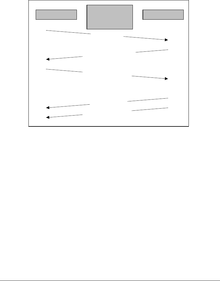
© SENSITECH INC. CONFIDENTIAL – CONTROLLED DOCUMENT
Page 66 of 83
A Carrier Corp. Company
PART NUMBER T82002163
REV A
communications. The figure below illustrates a typical Omega TT4 Standard
Command exchange between the host and monitor:
Executes
Command
Command
Echo back command
0x00 or parameters
Status
Any additional data
HOST PC MONITOR
TT4 PLUS
STANDARD
COMMAND
PROTOCOL
As can be seen in the diagram, the host initiates a command by sending a command value
to the monitor. The monitor then echoes back the same command value. This way
the host device will know that the unit received a specific command value correctly.
If the unit echoes back the wrong command value, the host computer merely ends
communications, thereby forcing the monitor to timeout.
If the host receives the correct command value back from the monitor, the host will send
either a 0h or command parameters. If a command requires parameters, such as the
“Write Scratchpad” command, the host computer upon receiving the echoed back
command would send the parameters at this time. For commands that do not require
any parameters, the host will send a 0h to act as a go signal.
Once the parameters or the 0h have been received, the monitor will then internally
execute the command and return a status byte followed by any additional data.
A status byte is always returned from the monitor upon completing a command whether
or not there is any additional data. The status byte is always a single byte value. A
0h value indicates successful completion of the command while a non-zero value
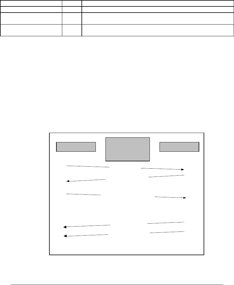
© SENSITECH INC. CONFIDENTIAL – CONTROLLED DOCUMENT
Page 67 of 83
A Carrier Corp. Company
PART NUMBER T82002163
REV A
indicates an error. A list of valid status codes with their names and descriptions are in
the table below:
Status name Code Description
CMD_SUCCESSFUL 0x00 Returned upon successful completion of command.
CMD_UNKNOWN 0x02 The requested command is not part of the unit's API. This is returned
when a command does not exist.
BAD_INIT 0x07 The unit cannot be initialized due to erroneous information having been
stored in its configuration pages.
Depending on the command that was sent, the monitor may or may not send data after the
status code. For instance, if the high-speed download command is sent to the
monitor, the monitor will send all of the temperature data after the status code has
been sent.
The Omega TT4 also supports a new packet based command protocol which uses the
same basic structure as the Omega TT4 standard commands with the exception that
the command parameters and return data are in packet form with a checksum
attached. If the command has parameters then the host sends the command parameter
packet just after the monitor echoes back the command value. If the command
returns any data, then the monitor will return the data packet just after the status is
sent. The following figure illustrates this:
Executes
Command
Command
Echo back command
0x00 or
Parameter Packet with
Checksum
Status
HOST PC MONITOR
TT4 Plus
PACKET
COMMAND
PROTOCOL
Data Packet With
Checksum
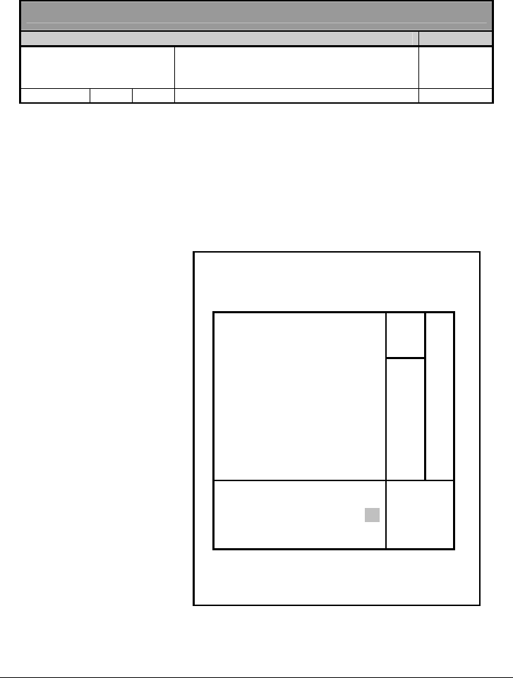
© SENSITECH INC. CONFIDENTIAL – CONTROLLED DOCUMENT
Page 68 of 83
A Carrier Corp. Company
PART NUMBER T82002163
REV A
The command parameter packet and data packet use the same packet format, which is
shown below:
Packet
Packet Data Checksum
3 byte count of the number of
parameters or data bytes to
follow Parameter or Data bytes
B0 B1 B2 D0, D1, D2, D3, ……….Dn 1Byte
For instance if a Omega TT4 command to download all the data is sent to the monitor,
the monitor will send (after the status byte) a packet containing a 3-byte value
representing the number of data bytes to follow, the data (which includes summary
information and temperature data), and a checksum.
For any packet, the checksum is the least significant byte of the sum of all the data in the
packet including the 3-byte count. This is shown in the example below:
If the packet contains 1120 data bytes and the value of
all the bytes is a hex 76 then the sum of the count bytes
and data bytes is as follows:
Count Byte 0 0x60
Count Byte 1 0x04
Count Byte 2 0x00
460H
(1120D)
Data Byte 0 0x76
Data Byte 1 0x76
Data Byte 2 0x76
. .
. .
. .
Data Byte 1119 0x76
Data Byte 1120 0x76
Data
Packet Data
Sum equals 0x208A0
Sum
Once the sum has been calculated, only the least
significant byte, in this case 0xA0, is used as the
checksum.
© SENSITECH INC. CONFIDENTIAL – CONTROLLED DOCUMENT
Page 69 of 83
A Carrier Corp. Company
PART NUMBER T82002163
REV A
TT4 Optical Interface Circuit
The circuit consists of a NAND gate IC which inverts the TX signal (input).
The input UP_UARTC_TX (B) is High and the input (A) is High, then the output is Low and the LED
will not conduct. However, when the TX line transitions from a High to Low state, then the NAND
gate output is High which the LED will begin to conduct.
The UP_UARTC_RX line is Low when light turns the Phototransistor ON. However, when there is no
light, the Phototransistor is OFF; therefore, the UP_UARTC_RX line is High.
LCD
The Trip Strip II will incorporate a monochrome FSTN 320 x 240 Transflective LCD display which will
allow the user to display the temperature/humidity graph of a downloaded monitor.
EDT LCD
LogicPD Evaluation
Board (J11)
VDD 1 4 3.3V
VSS 2 1 DGND
VLCD 3 Booster Power Supply VLCD (boost/pot output)
FLM 4 28 LCD_VSYNC
n/c 5 n/c
CL1 6 30 LCD_HSYNC
CL2 7 32 LCD_DCLK
D0 8 26 B4
D1 9 24 B3
D2 10 23 B2
D3 11 22 B1
DISPOFF 12 35 LCD_MDISP
VLED 13 3 5V
VLSS 14 1 DGND

© SENSITECH INC. CONFIDENTIAL – CONTROLLED DOCUMENT
Page 70 of 83
A Carrier Corp. Company
PART NUMBER T82002163
REV A
Interface Signals:
Pin No. Symbol Function
1 VDD POWER SUPPLY FOR LOGIC CIRCUIT
2 VSS GROUND
3 VLCD POWER SUPPLY FOR LCD DRIVING VOLTAGE
4 FLM THE FLM SIGNAL INDICATING THE BEGINNING OF
EACH DISPLAY CYCLE
5 N/C N/C
6 CL1 DISPLAY DATA LATCH
7 CL2 DISPLAY DATA SHIFT
8 D0 DISPLAY DATA
9 D1 DISPLAY DATA
10 D2 DISPLAY DATA
11 D3 DISPLAY DATA
12 /DISPOFF CONTROL LCD ON/OFF
“L”: DISPLAY OFF,
“H” DISPLAY ON
13 VLED POWER SUPPLY FOR LED B.L
14 VLSS POWER SUPPLY FOR LED B.L
Switching Characteristics:
PARAMETER SYMBOL MIN. TYP. MAX UNIT
CL1 PULSE
WIDTH tw1 30 - - ns
CL2 PULSE tw 51 - - ns
RISE, FALL
TIME tr, tf - - 50 ns
DATA SETUP
TIME tDSU 30 - - ns
DATA HOLD
TIME tDHD 40 - - ns
CL1 SETUP TIME tLSU 51 - - ns
CL1 to CL2 TIME tLC 51 - - ns
FLM SETUP
TIME tsetup 30 - - ns
FLM HOLD TIME thold 50 - - ns
LCD Power ON Sequencing:
1. Logic Circuit Power Supply 3.3VDC (no GPIO)
2. Data Signals (no GPIO)
3. LED Back Light Power Supply 5VDC (GPIO 22, LCD_BL_EN)
4. LCD Contrast Power Supply 3.3VDC (GPIO 12, VLCD_EN)
5. LCD Enable Signal “CONTROL LCD ON/OFF” (GPIO 77, LCD_MDISP)
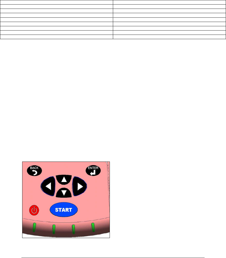
© SENSITECH INC. CONFIDENTIAL – CONTROLLED DOCUMENT
Page 71 of 83
A Carrier Corp. Company
PART NUMBER T82002163
REV A
Keypad
The keypad will consist of 8 buttons which will provide control of the following functions. There are 5
keys that will be dedicated to the navigation of the LCD selections consisting of an up, down, right, left and
OK or select. The three remaining keys will control the power (ON/OFF), Print (START), and BACK. The
method of communication with the Logic PD from the keypad will be in the form of GPIO interrupts. See
the chart below for clarification:
TSII Keypad rows0-2 and columns0-2 identification 06/20/08
Reference: Schematics V3.4.7
KEY IDs: row X, column Y
BACK row 0, column 1
PRINTER row 0, column 2
UP row 1, column 0
DOWN row 1, column 1
ENTER/OK row 1, column 2
LEFT row 2, column 0
RIGHT row 2, column 1
Power Charge Paper Low Batt
Rev 5.27.08
BUTTONS FUNCTIONS
1. BACK 1. Navigate to previous window or selection. Cancel.
2. ENTER 2. Execute command/entry. Executes menu structure.
3. UP Arrow 3. Navigate up
4. DOWN Arrow 4. Navigate down
5. LEFT Arrow 5. Navigate left
6. RIGHT Arrow 6. Navigate right
7. START 7. Download TT4 or TTmini and Print data
8. POWER 8. Initiate power to the unit or power OFF
© SENSITECH INC. CONFIDENTIAL – CONTROLLED DOCUMENT
Page 72 of 83
A Carrier Corp. Company
PART NUMBER T82002163
REV A
9.0 Battery Low Alert Function:
The Trip Strip II has a LED indicator which will indicate a low battery condition by steady red LED.
The circuit is comprised of two Comparators. If the Vin(+) terminal is Low and the Vin(-) terminal is High,
then the output is Low (current will flow). However if the Vin(+) terminal is High and the Vin(-) terminal
is Low, then the output is High (current will not flow).
Therefore, If the Load in the variable input (5 – 27VDC) is <= 6.5VDC, then the Low Batt LED will be
ON. However, if the variable input is >6.8VDC, then the Low Batt LED is OFF. The other input VB =
3.3VDC, which is a fixed input.
If the variable input voltage (Load) is <=6.0VDC, then the Q107 FET (P-Channel) will close.
10.0 Line Thermal Head Printer:
Citizen model # MLT-289 50mm thermal print head without the paper cutting functionality.
Head Temperature Detection Thermistor
Paper End Detection Photointerruptor (LED Indication)
Head-Up Detection Mechanical Switch
Vp = 6.25VDC
Vdd = 5VDC
The thermal head is comprised of heating elements and the head drivers that drive the heating elements.
Serial print data, fed to the SI input, is shifted into the register synchronized with the Shift clock, then is
latched into the latch register at the active edge of the LATCH signal. The Head Drive signal (Print
commands STR1-6) opens the gate to energize the heating elements reflecting the print data.
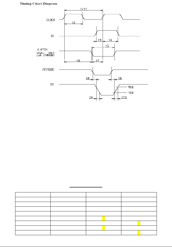
© SENSITECH INC. CONFIDENTIAL – CONTROLLED DOCUMENT
Page 73 of 83
A Carrier Corp. Company
PART NUMBER T82002163
REV A
Motor driving pulse rate:
Motor driving speed varies with driving voltage. It is determined with the following formula:
Motor driving speed (pps) = [200 * (Vp) – 600]
Therefore, for our application Vp = 6.25VDC.
As a result, [200 * (6.25) – 600] = 650 pps
11.0 Control Board
Dip Switch Setting:
Pin No. Function ON OFF
DS1-1 Auto Cutter X
1-2 CR Selection X
1-3 Print Density X
1-4 DTR/XON-XOFF X
1-5 Baud Rate X
1-6 Baud Rate X
1-7 Baud Rate X
1-8 Baud Rate X
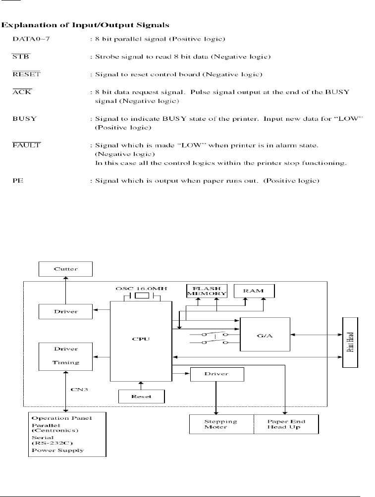
© SENSITECH INC. CONFIDENTIAL – CONTROLLED DOCUMENT
Page 74 of 83
A Carrier Corp. Company
PART NUMBER T82002163
REV A
Note: 1-5 to 1-8 configurations (above) indicate 19,200 bps Baud Rate.
When BUSY signal is “LOW”, data from the host can be received. During a “HIGH” state, data cannot be
received.
This control board incorporates a 2K byte buffer. Therefore, large amount of data can be buffered in input
buffer and the Host side can be released immediately.
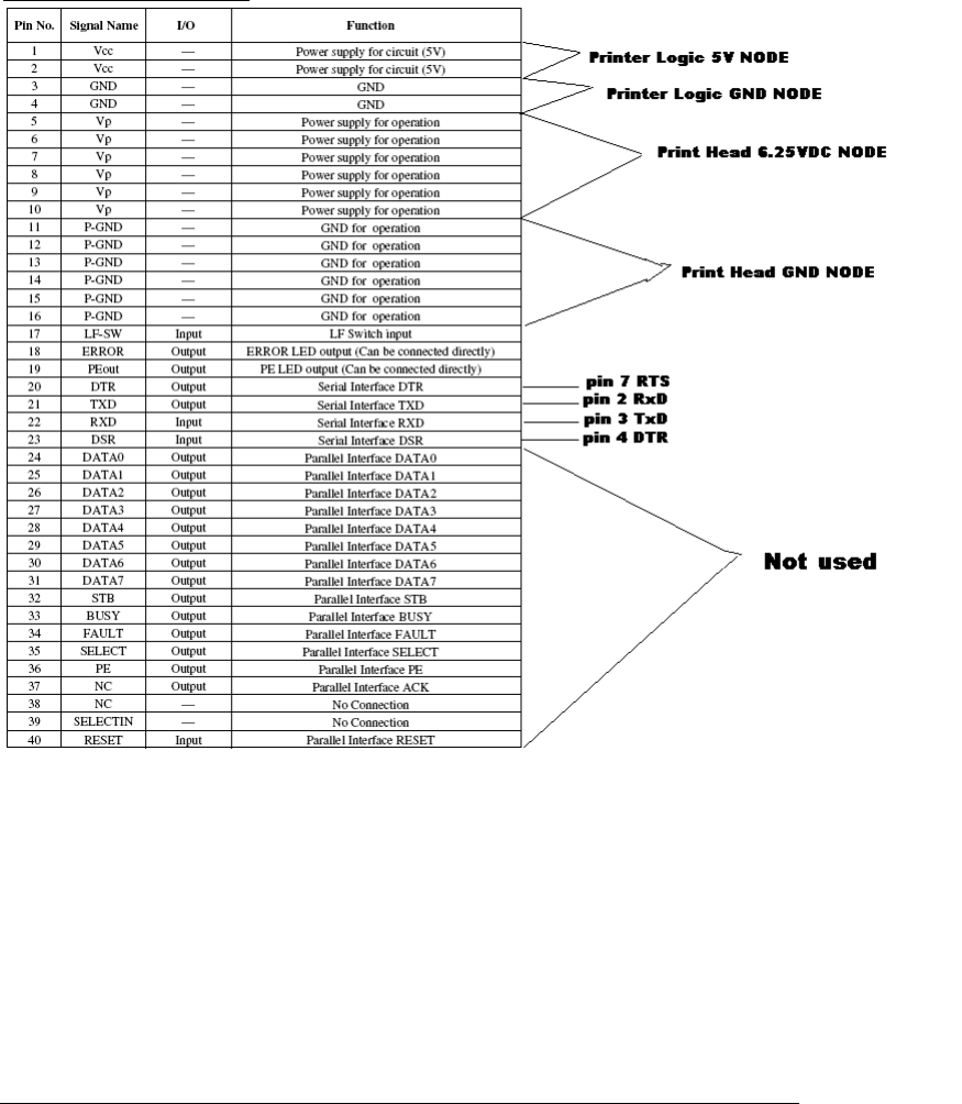
© SENSITECH INC. CONFIDENTIAL – CONTROLLED DOCUMENT
Page 75 of 83
A Carrier Corp. Company
PART NUMBER T82002163
REV A
Printer Control Board Pinouts:

© SENSITECH INC. CONFIDENTIAL – CONTROLLED DOCUMENT
Page 76 of 83
A Carrier Corp. Company
PART NUMBER T82002163
REV A
Device System Configuration Information
LogicLoader (LoLoTM)
LogicLoader Overview
The LogicLoader (LoLo) is a bootloader/firmware-monitor program developed by Logic Product
Development. LogicLoader is designed to initialize an embedded device, load and bootstrap an
operating system, and provide a low-level firmware monitor with debugging functionality.
LogicLoader Basics
Most operating systems rely on an underlying bootloader to initialize a device from its reset condition. In
general, operating systems are designed with the assumption that the system will be in a specific pre-
defined state before the operating system is started. Some example assumptions might be that system
RAM has been initialized and cleared, processor interrupts are disabled, and a timer has been
initialized to provide a system tick for the OS. The LogicLoader program initializes Logic Product
Development’s SOM platforms and prepares them for use by an operating system.
Another basic function of LogicLoader is the capability to upgrade device software (flash memory, CPLD
firmware, serial EEPROM contents) after deployment. This “in-field upgrade” ability requires a
bootloader program that is capable of loading software images from various sources as well as
committing loaded images to non-volatile memory. LogicLoader implements this by giving the system
the ability to load system software from flash memory, a CompactFlash storage card, a Local Area
Network, or even from a device attached to the system’s serial port. LogicLoader also has the ability to
upgrade an existing operating system residing in system flash.
LogicLoader was developed to fulfill the need for an OS and processor independent bootloader that can
interface with a variety of hardware transports. The GNU development tool chain used to build
LogicLoader is cross-platform capable.
Using LogicLoader for Debugging
LogicLoader implements a feature-rich firmware monitor. Included with LoLo is the LogicLoader shell,
also known as “losh.” Losh is a command interpreter providing control over system state prior to
loading an OS image. It has features such as command recall, command-line editing, automated
control via scripting, and diagnostic routines.
Losh includes many commands designed specifically to help software and hardware engineers debug low-
level interfaces. For example, formatted data in arbitrary memory locations can be read from, and
written to, by using the 'x' and 'w' commands. Other commands run specific tests designed to verify
Logic’s SOM hardware platforms. All commands return a value to the command line that can be used
to conditionally evaluate the command result. Refer to the LogicLoader Command Description Manual
on Logic’s downloads page for a complete description of available commands.
Developers may code their own test programs using the provided GNU development tool chain and use the
LogicLoader to load and run their software. This provides the ability to verify and debug hardware
interfaces without the overhead of building, downloading, and running large operating system images.
Manufacturing Advantages with LoLo
LogicLoader can be used with a desktop software utility to load a device’s system software on the
manufacturing line. This utility is customizable to suit your desired transfer mechanism and additional

© SENSITECH INC. CONFIDENTIAL – CONTROLLED DOCUMENT
Page 77 of 83
A Carrier Corp. Company
PART NUMBER T82002163
REV A
needs. LogicLoader can also be augmented with functional test software to completely verify a device
before it leaves the manufacturing line. Here is an example scenario: LogicLoader could launch a
device’s final functional test at the end of a manufacturing line, and then load the device’s final
software image before packaging. Contact Logic for more information on using LogicLoader to
streamline manufacturing.
The LogicLoader Shell (loshTM)
Losh Overview
Losh is a command interpreter similar to those found in Unix environments. Losh implements a
rudimentary network and file system command set, enhanced with custom diagnostic and memory
manipulation commands for debugging hardware.
Developers familiar with a Unix-like command line interface should find the losh implementation familiar
and easy to work with. Many of losh’s commands are patterned after their Unix counterparts and share
the same syntax.
Losh Basics
Losh uses a standard output stream (stdout). By default, stdout refers to a SOM’s debug serial port. The
output of any command that displays information to stdout (i.e. the ‘cat’ command) can be viewed
using the terminal emulation program connected to the SOM’s debug serial port. Likewise, the
standard input stream (stdin) by default also refers to the SOM’s debug serial port.
The LogicLoader Shell includes a virtual file system that uses standard Unix path names. The highest-level
(or root) directory is designated by the identifier ‘/’. A special sub-directory of the root with the name
‘dev’ is used to enumerate and interact with system’s various peripherals and their associated device
drivers.
Using Losh
The losh shell includes a basic command line editing feature and a command history feature. This provides
users with a quick way to repeat commands. Using the up and down arrow keys, the user can scroll
through the list of previously executed commands. When a desired command is displayed, press the
return key to repeat the command. The right and left arrow keys allow a user to position the cursor as
desired on the current line so that text can be modified, deleted, or inserted at the appropriate location
without having to “backspace” the entire line to access the portion of the command or command set
being entered.
Losh includes a user help feature through the ‘help’ command. Typing ‘help’ followed by any command
name at the losh prompt will display the command’s syntax, usage, and an example. This may be
especially helpful to users who are just becoming familiar with the LogicLoader shell.
Commands may be run in the background by adding a ‘&’ suffix.
Program Loading
Using LogicLoader to download any application, operating system, or update to a device requires an
understanding of the interaction between the ‘load’, ‘burn’, ‘jump’, and ‘exec’ commands. The
purpose of this section is to explain the interaction of these commands.
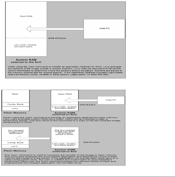
© SENSITECH INC. CONFIDENTIAL – CONTROLLED DOCUMENT
Page 78 of 83
A Carrier Corp. Company
PART NUMBER T82002163
REV A
4.1 Understanding the Load Command
The purpose of the ‘load’ command is to transfer an executable image to a device. The image must be in
one of the following supported formats: ELF, SREC, RAW, or BIN. The ‘load’ command uses
information inherent to the supported formats (or as entered as part of the command for RAW format)
to determine where in the device’s memory the downloaded image should be stored. The image must
be destined to run from either flash memory, system RAM, or on-chip SRAM.
If an image is destined for system RAM or on-chip SRAM, the ‘load’ command stores the image directly to
its run-time location. Refer to Figure 4.1: Downloading to RAM for a graphic representation of this
process.
If a downloaded application is destined for flash memory, the ‘load’ command transfers the file into a
temporary RAM buffer on the device. The transferred image may be programmed into flash using the
‘burn’ command after the transfer is complete. Refer to Figure 4.2: Downloading to Flash for a graphic
representation of this process.
Figure 4.1: Downloading to RAM
Figure 4.2: Downloading to Flash

© SENSITECH INC. CONFIDENTIAL – CONTROLLED DOCUMENT
Page 79 of 83
A Carrier Corp. Company
PART NUMBER T82002163
REV A
YAFFS (Yet Another Flash File System)
8.1 YAFFS Overview
The acronym YAFFS stands for the phrase "Yet Another Flash Filing System." YAFFS was developed by a
company named Aleph One Limited and incorporated by Logic Product Development into the LogicLoader
(LoLo) software program.
Logic selected YAFFS to fill its file system requirements due to the flexible nature of the program, its
licensing scheme, and the fact that it is available for Linux, Windows CE, and other operating systems.
YAFFS also allows LogicLoader and an RTOS to view and modify the same partition. It also makes it
easier for customers to work with embedded flash technology and perform in-field updates.
Note: The partition entries for YAFFS partitions are not persistent -- they must be restored on each boot.
However, the partitions and data remain persistent.
8.2 Working with YAFFS in LogicLoader
8.2.1 Developing a Partition Scheme
The LogicLoader may mount up to four YAFFS partitions at a time. Customers should design a partitioning
scheme which suits their individual needs. The following limits are imposed on partitions:
• Each partition must have a unique name.
• Each partition must exist on local flash accessible from LogicLoader’s '/dev/flashx' device file
(where ‘x’ is an instance index). For example: /dev/flash0 or /dev/flash1.
• Each partition must span at least 4 physical flash blocks.
• A partition must not overlap the flash blocks that contain LogicLoader or its configuration block.
For information about the location of these items, check the LogicLoader User's Manual
addendum for your hardware.
For the remainder of this document, the following partitioning scheme for demonstration purposes will be
used:
• A partition named 'boot' which contains a bitmap and operating
system image and spans the address space below:
* start: 0x000C0000
* length: 0x00800000 (8 MBytes)
• A partition named 'data' which contains customer specific data.
* start: 0x00900000
* length: 0x00400000 (4 MBytes)

© SENSITECH INC. CONFIDENTIAL – CONTROLLED DOCUMENT
Page 80 of 83
A Carrier Corp. Company
PART NUMBER T82002163
REV A
8.2.2 Formatting YAFFS Partitions
All file systems need to be formatted before they can be mounted. Because YAFFS was designed from the
ground up to work with embedded flash technologies, it understands an 'erased' flash device to be both
formatted and empty. To prepare your partition for mounting, simply use LogicLoader's 'erase' command to
erase the area of flash where the partition is to be located.
Using the example partition scheme in the “Developing a Partition Scheme” section, above, the partitions
could be prepared for initial use by erasing the regions of the flash device spanned by them.
For example (LH7A404-11 system address used): losh> erase 0x000C0000 0x00800000
losh > erase 0x00900000 0x00400000
Warning: Erasing flash blocks that will be used for YAFFS partitions will erase everything in those areas of
flash. It is not required to format the partition every time the device is rebooted. The partition should only
be formatted when an entirely new YAFFS partition is created, or when the data on a stored partition needs
to be completely erased.
8.2.3 Adding YAFFS Type Partitions
LogicLoader maintains a partition table in RAM. Before a YAFFS partition can be mounted, it must be
added to the partition table. To do this, the 'add-yaffs' command is used. The 'add-yaffs' command takes the
following arguments:
• <name> a unique string which identifies the partition
• <type> type of flash device the partition resides on
• <start> the physical starting address of the partition
• <length> the length (in bytes) of the partition
Continuing with the example partitions above, LogicLoader can be instructed to add the partitions by
executing the commands as shown below (LH7A404-11 system address used):
losh> add-yaffs boot nor 0x000C0000 0x00800000
losh> add-yaffs data nor 0x00900000 0x00400000
Note: The above steps must be performed every time LogicLoader boots. Because LogicLoader keeps the
partition table in RAM, the existence and locations of YAFFS partitions does not persist across resets or
power cycles.
8.2.4 Mounting the Partition
To mount a partition in the partition table, the 'mount' command is used. That command takes the following
arguments:
• <fstype> the type of filesystem being mounted (‘yaffs’ here)
• [drive addr] not used when mounting a YAFFS partition
• <point> the name of the YAFFS partition
For example:
losh> mount yaffs /boot

© SENSITECH INC. CONFIDENTIAL – CONTROLLED DOCUMENT
Page 81 of 83
A Carrier Corp. Company
PART NUMBER T82002163
REV A
losh> mount yaffs /data
Of note is that the 'drive addr' argument is not used when mounting a YAFFS partition. Also of note is that
the 'point' argument needs to correspond to the name of the partition (as defined by the add-yaffs
command) preceded by a forward slash. LogicLoader needs to mount all YAFFS partitions at the root-
directory level. Thus, a partition added using:
'add-yaffs boot ...'
will be mounted using:
'mount ... /boot'.
Note the absence of the '/' character during the 'add-yaffs' command and its presence during the 'mount'
command.
8.2.5 Accessing YAFFS Partitions in an OS
A key advantage of the read/write YAFFS filesystem capability at the LogicLoader level is the ability to
share data stored in the filesystem with an OS environment. If an OS environment (e.g. Linux, WinCE,
VxWorks) implements YAFFS as an OS-accessible file-system, any files available to LogicLoader are
also available to the OS, and vice-versa.
This contributes to significant benefits in the areas of system software upgrades (including OS upgrades)
splash screen changes, script modifications, and other boot-time data that may need to be updated.
8.3 Summary
To use the YAFFS file system within LogicLoader, follow these steps:
1) Decide on a partitioning scheme.
2) Format the partitions by erasing the associated flash blocks.
3) Add the partitions to LogicLoader using the 'add-yaffs' command.
4) Mount the partitions using the 'mount' command.
Steps 3 and 4 must be repeated every time the system is booted. If the YAFFS partitions are frequently
accessed, consider implementing steps 3 and 4 via a boot script. Step 2 only needs to be performed when
creating a brand new partition or when the contents of an existing partition need to be completely erased.
Note: a partition is persistent. Re-adding a partition at boot-time restores access to previously saved data.
Flash blocks must be erased to permanently remove a partition; otherwise, it can be recovered across boots.
Keep in mind the following when working with YAFFS and LogicLoader:
• Ensure that a partition name does not begin with a '/'. LogicLoader’s virtual filesystem uses the
forward slash to indicate the root directory.
• Ensure partitions do not overlap each other, LogicLoader, or the configuration block.
• Ensure that a partition is erased before it is mounted for the first time.

© SENSITECH INC. CONFIDENTIAL – CONTROLLED DOCUMENT
Page 82 of 83
A Carrier Corp. Company
PART NUMBER T82002163
REV A
Explanation of Script
losh> erase B10 B256 /dev/nand0
Purpose of erase command:
This command erases non-volatile <device>. When using a memory mapped device (such as NOR flash)
the <start address> and <length> parameters indicate the memory address and the length in bytes. When
using a block device (such as NAND flash) the <start block> and <number of blocks> indicate the first
block number and the number of blocks to erase. Note; some devices, such as NAND flash, are marked
with bad blocks by the device manufacturer, these blocks will not be erased and the erase command will
indicate which blocks have been marked bad.
losh> add-yaffs boot nand B10 B256\
Purpose of add-yaffs command:
This command adds a YAFFS partition into LoLo's partition table. You must execute this command before
attempting to mount the YAFFS partition itself. When creating a partition in a NOR flash device, the start
location is a memory address and the length is in bytes. When creating a partition in a NAND flash device,
the start location is the start block and the length indicates the number of blocks.
This command must be called after a reset in order to make LoLo aware of a YAFFS partition. To create a
new YAFFS partition, use the erase command to erase the range of addresses containing the YAFFS file
system in flash memory before calling add-yaffs.
losh> mount yaffs /boot
Purpose of mount command:
This command mounts a filesytem of type <fstype> onto LoLo's root filesystem at point <point>. If the
mount command is successful, you may use other shell commands to access the new filesystem.
losh> erase B267 B128 /dev/nand0
Purpose of erase command:
This command erases non-volatile <device>. When using a memory mapped device (such as NOR flash)
the <start address> and <length> parameters indicate the memory address and the length in bytes. When
using a block device (such as NAND flash) the <start block> and <number of blocks> indicate the first
block number and the number of blocks to erase. Note; some devices, such as NAND flash, are marked
with bad blocks by the device manufacturer, these blocks will not be erased and the erase command will
indicate which blocks have been marked bad.
losh> add-yaffs data nand B267 B128
Purpose of add-yaffs command:
This command adds a YAFFS partition into LoLo's partition table. You must execute this command before
attempting to mount the YAFFS partition itself. When creating a partition in a NOR flash device, the start
location is a memory address and the length is in bytes. When creating a partition in a NAND flash device,
the start location is the start block and the length indicates the number of blocks.
This command must be called after a reset in order to make LoLo aware of a YAFFS partition. To create a
new YAFFS partition, use the erase command to erase the range of addresses containing the YAFFS file
system in flash memory before calling add-yaffs.
losh> mount yaffs /data
Purpose of mount command:
This command mounts a filesytem of type <fstype> onto LoLo's root filesystem at point <point>. If the
mount command is successful, you may use other shell commands to access the new filesystem.

© SENSITECH INC. CONFIDENTIAL – CONTROLLED DOCUMENT Page 83 of 83
A Carrier Corp. Company
PART NUMBER T82002163
REV A
losh> mount fatfs /cfs
Purpose of mount command:
This command mounts a filesytem of type <fstype> onto LoLo's root filesystem at point <point>. If the
mount command is successful, you may use other shell commands to access the new filesystem.
losh> cp /cf/NK.BIN /boot/NK.BIN
Purpose of cp command:
This command is used to copy a file.
losh> config CREATE
Purpose of Config command:
This command saves and/or displays configuration information in the config device. The config device
starts at offset 0x40000 in the boot flash device. The config device may be used to store a boot script, the
debug port baud rate settings, user defined video settings, and the debug Ethernet settings. Please consult
the LogicLoader User's Manual for a full explanation of the config block device.
Create creates a new config block
losh> echo "VOLOadd-yaffs boot nand B10 B256;mount yaffs /boot;add-yaffs data nand B267 B128;
mount yaffs/data;load bin /boot/NK.BIN;
exec rtc:rtc_pxa270:disp_num:0;exit;\n" /dev/config
Purpose of echo command:
This command echoes a string to standard output or to a file.
Note:
This command sets $@ to the number of characters written when no failure occurs.
Purpose of the exec command:
This command allows the processor to jump to an OS image loaded in memory or to a given address.
Before the jump, interrupts, memory caching, and mapping are disabled.
Note:
Returns the return value of the executed code and sets $@ to the jump address when no losh errors occur.
The disp_num: value correlates to the LCD model being used. In this case, the disp_num is 0 for the EDT
LCD. However, for the LogicPD evaluation board LCD, the value is 3.
losh> VOLOadd-yaffs boot nand B10 B256;mount yaffs /boot;add-yaffs data nand B267 B128; mount
yaffs /data;load bin /boot/NK.BIN;exec rtc:rtc_pxa270:disp_num:0;exit;
This device complies with Part 15 of the FCC Rules.
Operation is subject to the following two conditions:
(1) This device may not cause harmful interference. and
(2) This device must accept any interference received, including interference that may cause undesired
operation