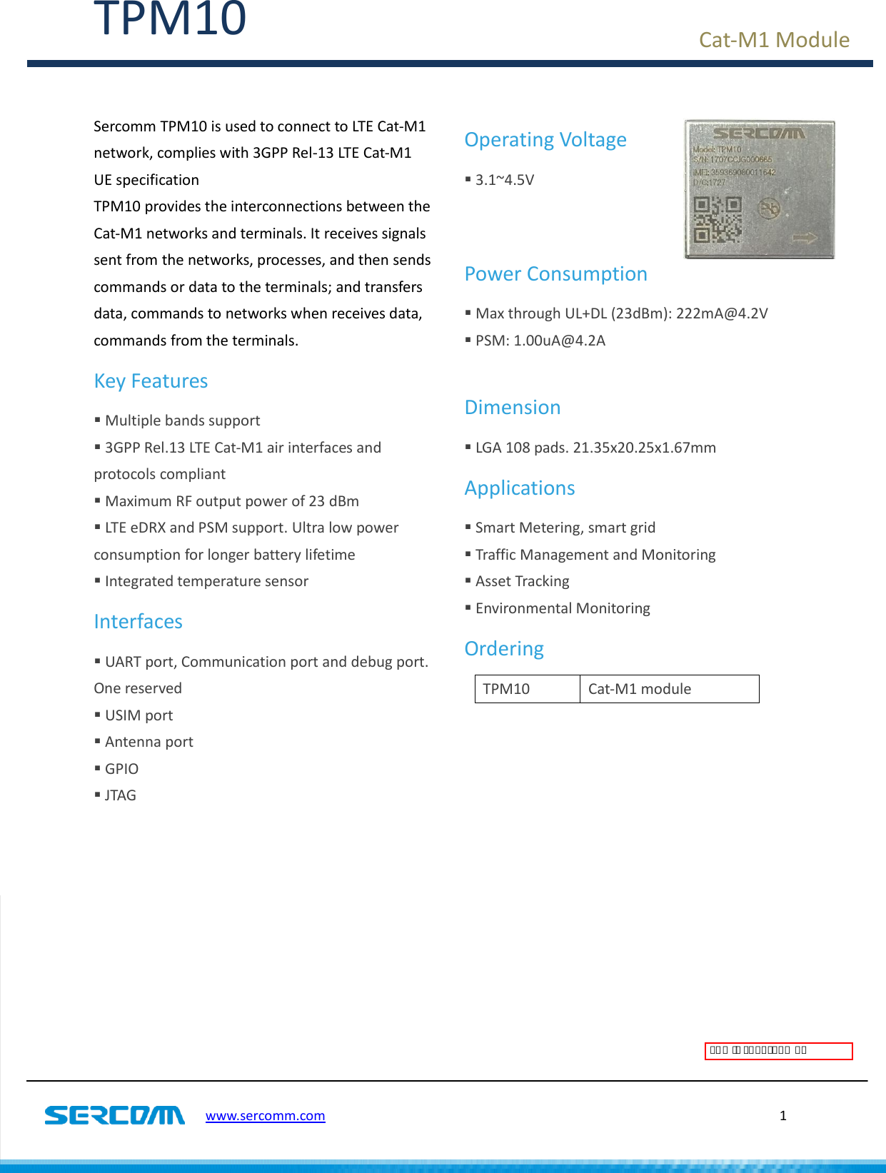
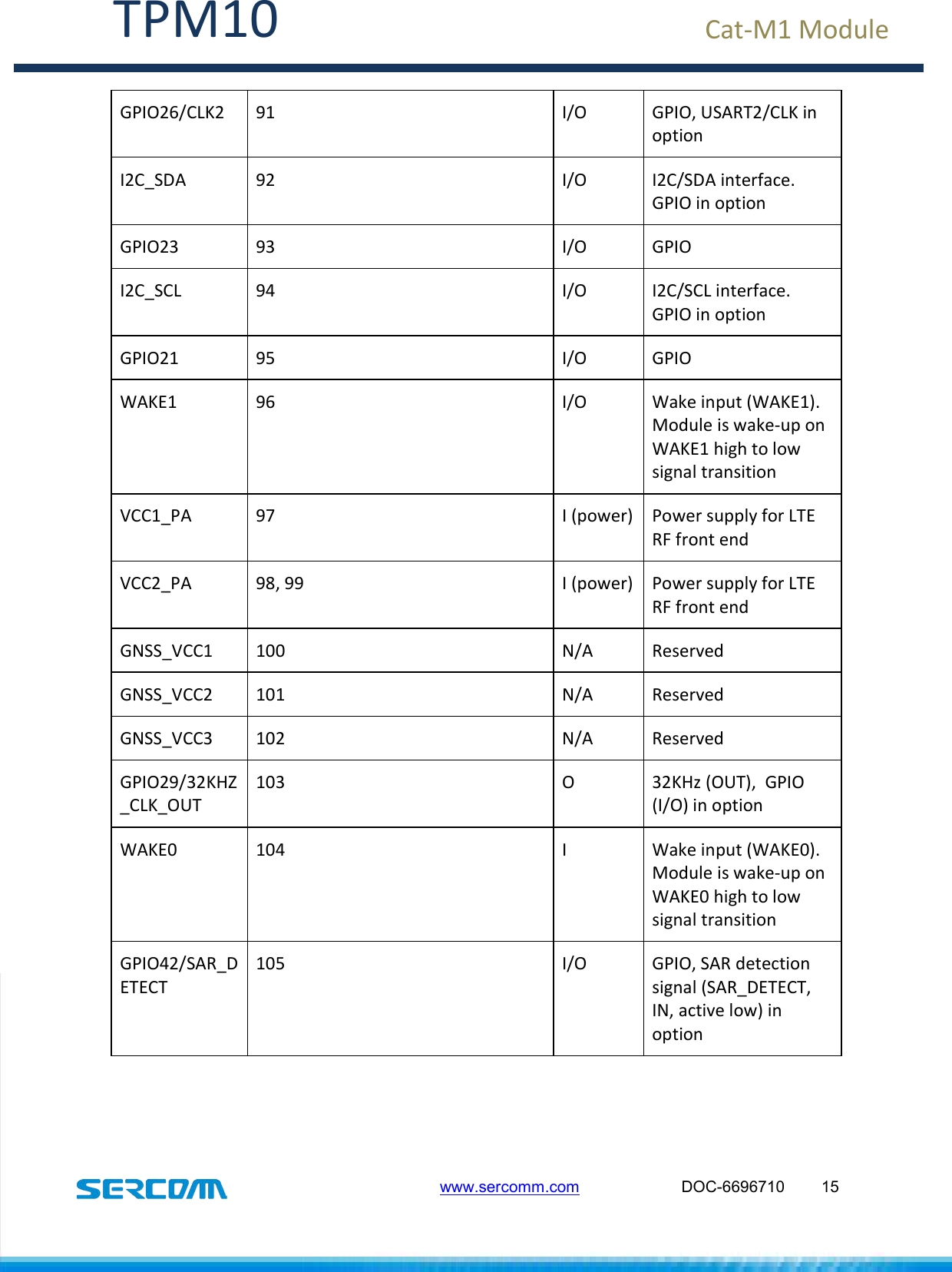
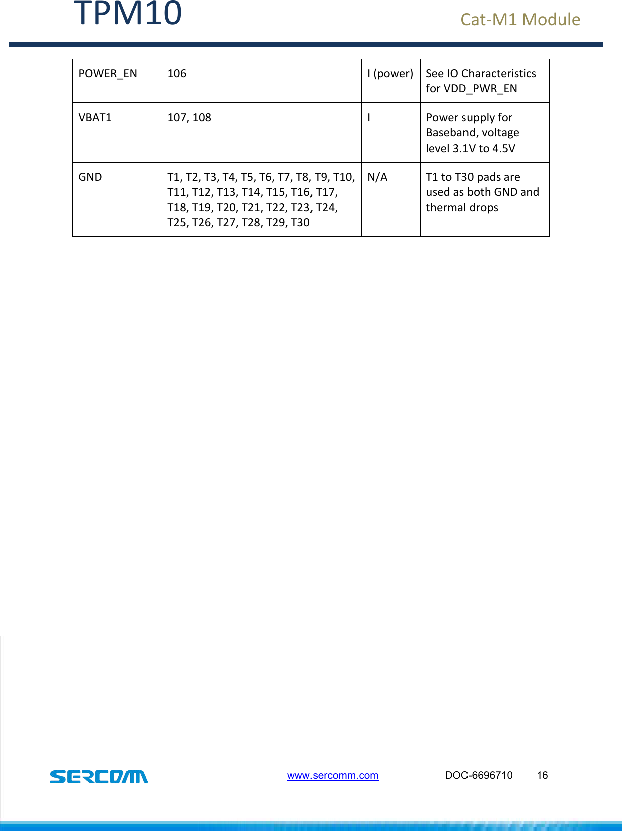
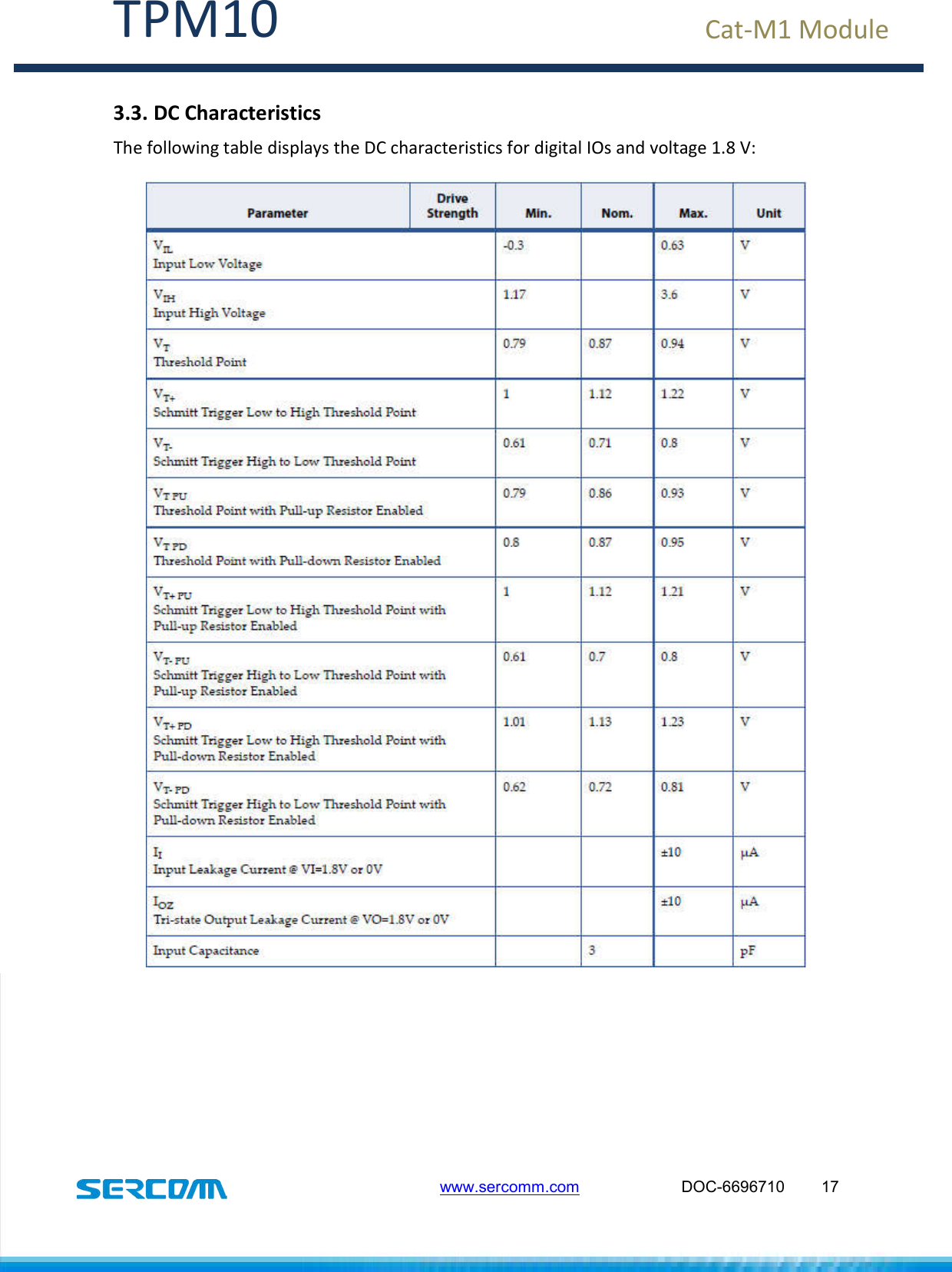
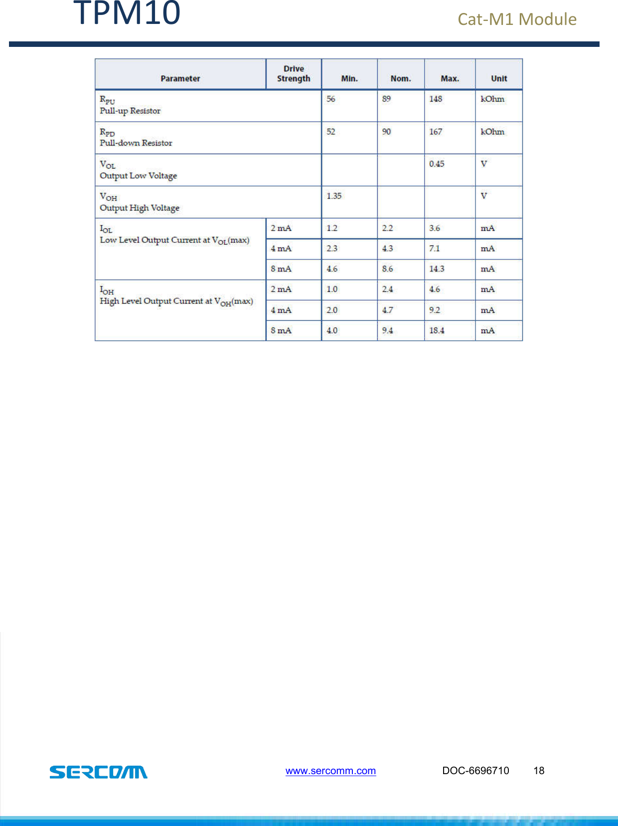
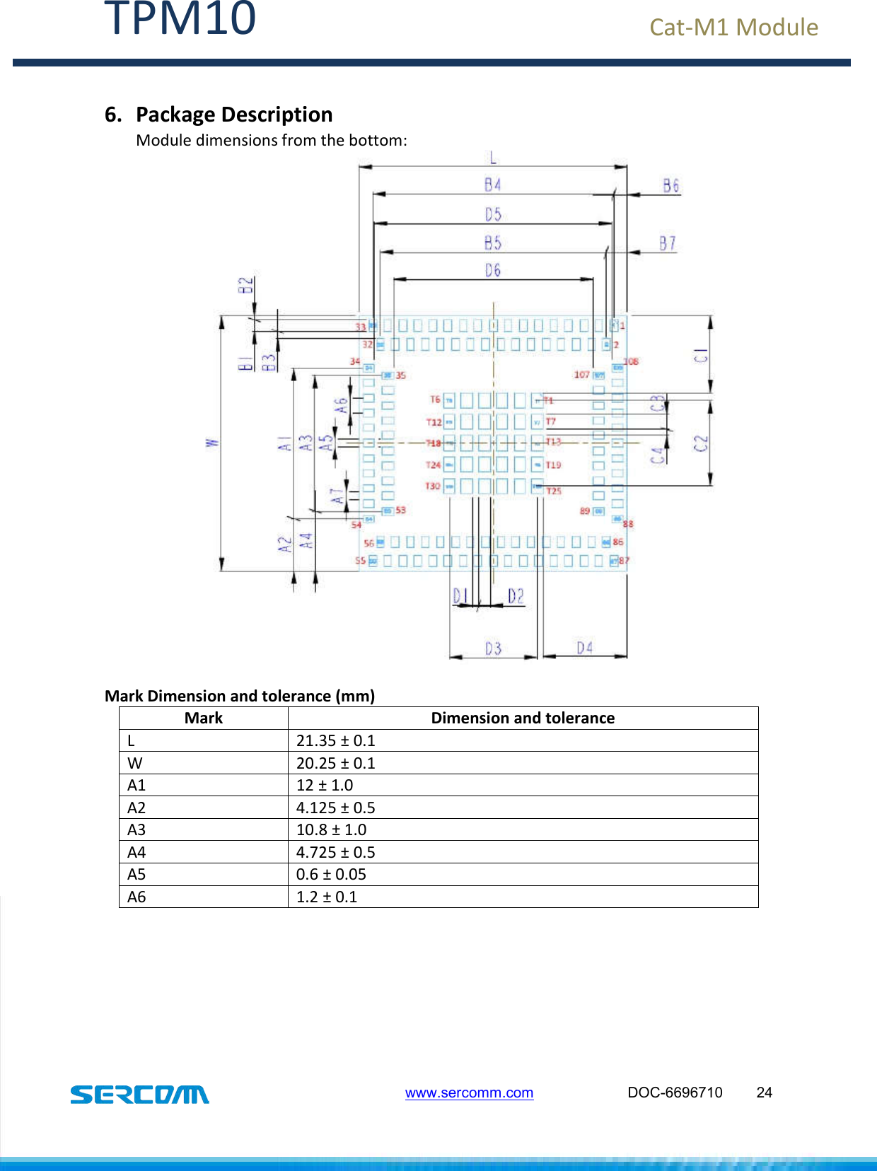
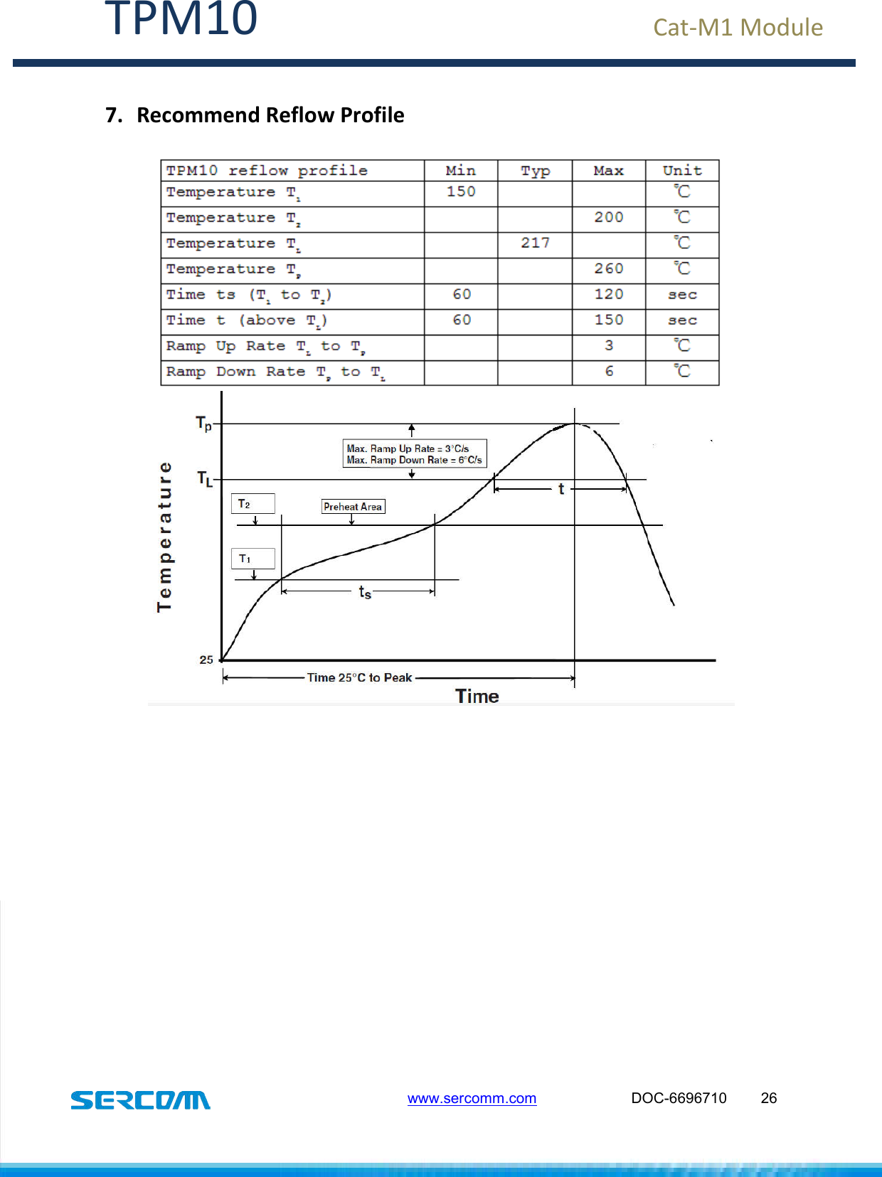
Sercomm TPM10 Cat-M1 Module User Manual

Sercomm Corporation Cat-M1 Module
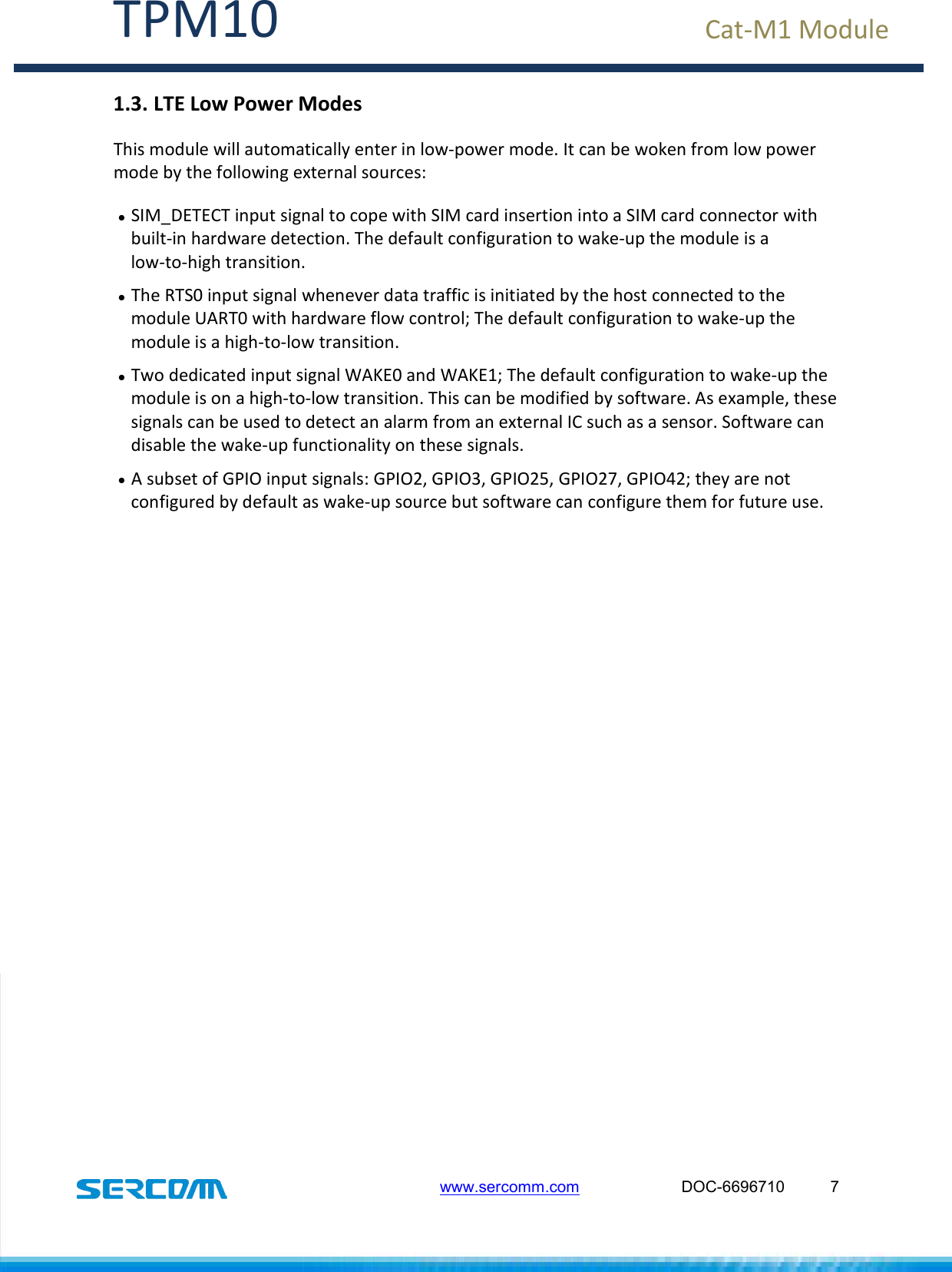
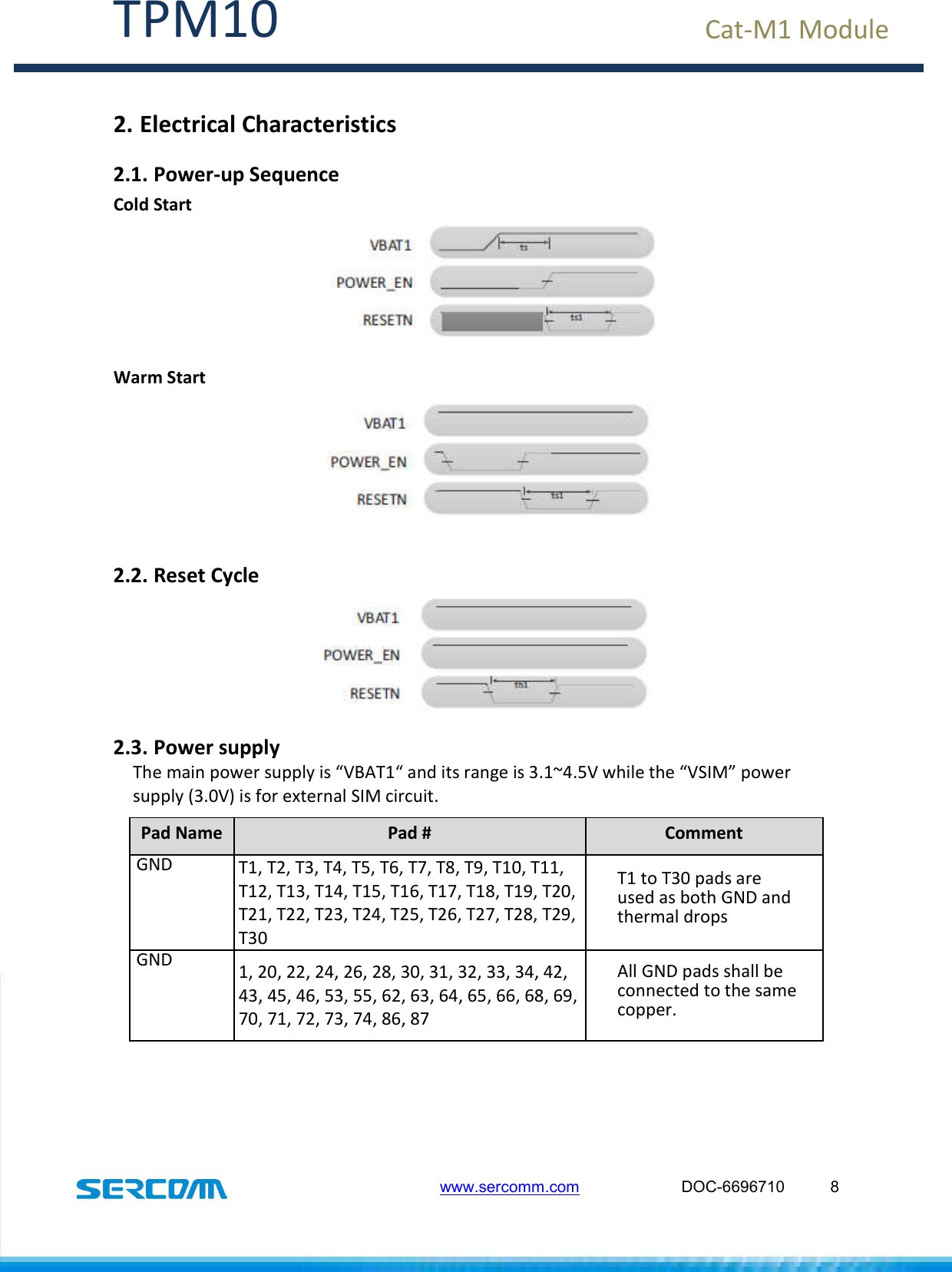
User Manual

 TPM10                    www.sercomm.com                                         1 Cat-M1 Module   Sercomm TPM10 is used to connect to LTE Cat-M1 network, complies with 3GPP Rel-13 LTE Cat-M1 UE specification TPM10 provides the interconnections between the Cat-M1 networks and terminals. It receives signals sent from the networks, processes, and then sends commands or data to the terminals; and transfers data, commands to networks when receives data, commands from the terminals. Key Features  Multiple bands support  3GPP Rel.13 LTE Cat-M1 air interfaces and protocols compliant  Maximum RF output power of 23 dBm    LTE eDRX and PSM support. Ultra low power consumption for longer battery lifetime  Integrated temperature sensor   Interfaces  UART port, Communication port and debug port. One reserved  USIM port  Antenna port  GPIO  JTAG   Operating Voltage  3.1~4.5V  Power Consumption  Max through UL+DL (23dBm): 222mA@4.2V    PSM: 1.00uA@4.2A  Dimension  LGA 108 pads. 21.35x20.25x1.67mm Applications  Smart Metering, smart grid    Traffic Management and Monitoring  Asset Tracking  Environmental Monitoring Ordering TPM10 Cat-M1 module         FCC ID: P27-TPM10
 TPM10                    www.sercomm.com                                         2 Cat-M1 Module  Federal Communication Commission Interference Statement  This  device complies with FCC  Rules. Operation  is subject  to  the  following  two  conditions:  (1)  This device may not cause harmful interference, and (2) this device must accept any interference received, including  interference  that  may  cause  undesired operation.  This  equipment  has  been  tested  and  found  to comply with the limits for a Class B digital device, pursuant to Part 15 of the FCC Rules.    These limits are  designed  to  provide  reasonable  protection against  harmful  interference  in  a  residential installation.  This  equipment  generates,  uses  and can  radiate  radio  frequency  energy  and,  if  not installed  and  used  in  accordance  with  the instructions,  may  cause  harmful  interference  to radio  communications.    However,  there  is  no guarantee  that  interference  will  not  occur  in  a particular  installation.    If  this  equipment  does cause  harmful  interference  to  radio  or  television reception, which can be determined by turning the equipment  off  and  on,  the  user  is  encouraged  to try  to  correct  the  interference  by  one  of  the following measures:   Reorient or relocate the receiving antenna.  Increase  the  separation  between  the equipment and receiver.  Connect  the  equipment  into  an  outlet  on  a circuit  different  from  that  to  which  the receiver is connected.  Consult  the  dealer  or  an  experienced radio/TV technician for help.  FCC Caution: Any  changes  or  modifications  not  expressly approved by the party responsible  for compliance could  void  the  user's  authority  to  operate  this equipment. This  transmitter  must  not  be  co-located  or operating  in  conjunction  with  any  other  antenna or transmitter. Radiation Exposure Statement: This  equipment  complies  with  FCC  radiation exposure  limits  set  forth  for  an  uncontrolled environment.  This  equipment  should  be  installed and  operated  with  minimum  distance  20cm between the radiator & your body.  This device is intended only for OEM integrators under the following conditions: 1) The antenna must be installed such that 20 cm is maintained between the antenna and users, and
 TPM10                    www.sercomm.com                                         3 Cat-M1 Module  2) The transmitter module may not be co-located with any other transmitter or antenna.  As long as 2 conditions above are met, further transmitter test will not be required. However, the OEM integrator is still responsible for testing their end-product for any additional compliance requirements required with this module installed  IMPORTANT NOTE: In the event that these conditions can not be met (for example certain laptop configurations or co-location with another transmitter), then the FCC authorization is no longer considered valid and the FCC ID can not be used on the final product. In these circumstances, the OEM integrator will be responsible for re-evaluating the end product (including the transmitter) and obtaining a separate FCC authorization.  End Product Labeling This transmitter module is authorized only for use in device where the antenna may be installed such that 20 cm may be maintained between the antenna and users. The final end product must be labeled in a visible area with the following: “Contains FCC ID: P27-TPM10”. The grantee's FCC ID can be used only when all FCC compliance requirements are met.  Manual Information To the End User The OEM integrator has to be aware not to provide information to the end user regarding how to install or remove this RF module in the user’s manual of the end product which integrates this module. The end user manual shall include all required regulatory information/warning as show in this manual. RF typical circuit The RF inter-connect called P1 is for example purposes only. Depending on the antenna, interfacing system will dictate the RF inter-connect. Below picture is showing RF typical circuit.  LTE-ANT0 is the primary(main) antenna pin and carries TX and RX signals. Connect 50 Ohm transmission lines from this pins to the 50 Ohm Primary Antenna/Antenna connetors.   The picture RF typical circuit shows, included in the connection between ANT and the antenna connectors, T-type network for matching.
 TPM10                                                   www.sercomm.com                       DOC-6696710  2  Cat-M1 Module    TPM10 DATASHEET       Specifications are subject to change without notice and should not be construed as a commitment by Sercomm Corporation  Copyright 2017 by Sercomm Corporation  All rights reserved.  Ver 1.0
 TPM10                                                   www.sercomm.com                       DOC-6696710  3  Cat-M1 Module  Revision History Rev  Date  Description V1.0  04/11/2017  Initial Release V1.0
 TPM10                                                   www.sercomm.com                       DOC-6696710  4  Cat-M1 Module Table of contents 1.  Functional Overview ........................................................................................................................ 5 1.1.  Block Circuit Diagram......................................................................................................... 5 1.2.  Main Module Components ................................................................................................ 6 1.3.  LTE Low Power Modes ....................................................................................................... 7 2.  Electrical Characteristics .................................................................................................................. 8 2.1.  Power-up Sequence ........................................................................................................... 8 2.2.  Reset Cycle ......................................................................................................................... 8 2.3.  Power supply ..................................................................................................................... 8 2.4.  Performance ...................................................................................................................... 9 3.  Pin out and Definitions .................................................................................................................. 10 3.1.  I/O Parameters Definition ............................................................................................... 10 3.2.  Module Pin Definition ...................................................................................................... 10 3.3.  DC Characteristics ............................................................................................................ 17 3.4.  UART Port ........................................................................................................................ 19 3.5.  SIM Port ........................................................................................................................... 20 3.6.  Antenna Port ................................................................................................................... 20 4.  ESD ................................................................................................................................................. 22 5.  EMC ................................................................................................................................................ 23 6.  Package Description ....................................................................................................................... 24 7.  Recommend Reflow Profile ........................................................................................................... 26 8.  Package and Storage Condition ..................................................................................................... 27 9.  Product Information ...................................................................................................................... 28 10.   Ordering Information .................................................................................................................... 29
 TPM10                                                   www.sercomm.com                       DOC-6696710  5  Cat-M1 Module 1. Functional Overview TPM10 module provides the interconnection between Cat-M1 networks and terminals.   Interconnection with Cat-M1 −  TPM10 module receives and processes signals sent from Cat-M1 networks, and then sends commands or data to terminals for performing the operation and maintenance (O&M).  −  The module receives data and commands from terminals, transferring those data and commands to Cat-M1 networks, and then delivers them to application servers (ASs).   Interconnection with terminals −  TPM10 module reads and uploads terminal data to the Cat-M1 networks.  −  The module receives commands from the Cat-M1 networks and performs O&M for terminals. 1.1.  Block Circuit Diagram TPM10 module is based on the SQN3330 Cat-M1 baseband and developed for 3GPP E-UTRA and Wireless LTE Cat-M1 UE specification. The image below shows the module block diagram:
 TPM10                                                   www.sercomm.com                       DOC-6696710  6  Cat-M1 Module  1.2.  Main Module Components The TPM10 includes the following components.  A. SQN3330 This module includes SQN3330 Cat-1 baseband, a complete dual band RF front end, memory and required circuitry to meet 3GPP E-UTRA (Long Term Evolution - LTE, Release 13 set of specifications) and Wireless LTE Cat-M1 UE specifications.  SQN3330 is a single-chip LTE Cat M1 solution, which is designed specifically for narrowband IoT applications, including sensors, wearables, and other low data, low power M2M and IoT devices.  B. RF  The RF matching circuit.  C. Power system  The main power supply is “VBAT1“ and its range is 3.1~4.5V while the “VSIM” power supply (3.0V) is for external SIM circuit. D. Clock in system  TPM10 is using 32KHz clock in the module system.
 TPM10                                                   www.sercomm.com                       DOC-6696710  7  Cat-M1 Module 1.3.  LTE Low Power Modes  This module will automatically enter in low-power mode. It can be woken from low power mode by the following external sources:   SIM_DETECT input signal to cope with SIM card insertion into a SIM card connector with        built-in hardware detection. The default configuration to wake-up the module is a      low-to-high transition.  The RTS0 input signal whenever data traffic is initiated by the host connected to the      module UART0 with hardware flow control; The default configuration to wake-up the      module is a high-to-low transition.  Two dedicated input signal WAKE0 and WAKE1; The default configuration to wake-up the      module is on a high-to-low transition. This can be modified by software. As example, these      signals can be used to detect an alarm from an external IC such as a sensor. Software can      disable the wake-up functionality on these signals.  A subset of GPIO input signals: GPIO2, GPIO3, GPIO25, GPIO27, GPIO42; they are not      configured by default as wake-up source but software can configure them for future use.
 TPM10                                                   www.sercomm.com                       DOC-6696710  8  Cat-M1 Module 2. Electrical Characteristics  2.1.  Power-up Sequence Cold Start    Warm Start     2.2.  Reset Cycle   2.3.  Power supply    The main power supply is “VBAT1“ and its range is 3.1~4.5V while the “VSIM” power supply (3.0V) is for external SIM circuit. Pad Name  Pad #  Comment GND T1, T2, T3, T4, T5, T6, T7, T8, T9, T10, T11, T12, T13, T14, T15, T16, T17, T18, T19, T20, T21, T22, T23, T24, T25, T26, T27, T28, T29, T30 T1 to T30 pads are used as both GND and thermal drops GND 1, 20, 22, 24, 26, 28, 30, 31, 32, 33, 34, 42, 43, 45, 46, 53, 55, 62, 63, 64, 65, 66, 68, 69, 70, 71, 72, 73, 74, 86, 87 All GND pads shall be connected to the same copper.
 TPM10                                                   www.sercomm.com                       DOC-6696710  9  Cat-M1 Module Pad Name  Pad #  Comment VBAT1  107, 108 Power supply for Baseband, voltage level 3.1V to 4.5V  2.4.  Performance  The Max output power of TPM10 is 23dBm +2/-2.7dBm  The typical sensitivity level of TPM10 is -103 dBm
 TPM10                                                   www.sercomm.com                       DOC-6696710  10  Cat-M1 Module 3. Pin out and Definitions 3.1.  I/O Parameters Definition  Type  Description DI Digital input DO Digital output I/O Bidirectional input/output AI Analog input AO Analog output PO Power output PI Power input OD Open drain  3.2.  Module Pin Definition Pad Name  Pad No.  I/O Type  Description GND  1, 20, 22, 24, 26, 28, 30, 31, 32, 33, 34, 42, 43, 45, 46, 53, 55, 62, 63, 64, 65, 66, 68, 69, 70, 71, 72, 73, 74, 86, 87 N/A  All GND pads shall be connected to the same copper. GPIO3/STATUS_LED 2  IN  GPIO or status LED (STATUS_LED, OUT) in option with 3 modes: - Activity based on LTE connectivity status (typically: ON when attached to LTE network) - Periodic pulse (Sign of life signal)  - LED switch off
 TPM10                                                   www.sercomm.com                       DOC-6696710  11  Cat-M1 Module 1V8  3  O (power) 1.8V reference voltage for IOs GNSS_VINB  4  N/A  Reserved RESERVED/FFF_FFH 5  I/O  Reserved pad GPIO2/POWER_MON 6  I/O  GPIO or Power monitor (POWER_MON, OUT) in option GPIO19/CLK0  7  I/O  GPIO, USART0/CLK in option GPIO27/CTS2  8  I/O  GPIO (I/O), USART2/CTS (OUT)  in option 3V0  9, 11  O (power) 3.0V power supply GPIO28/RTS2  10  I/O  GPIO (I/O), USART2/RTS (IN)  in option SIM_RESETN  12  O  SIM card interface: reset output pin for the SIM card DNC  13, 15  Do not connect Do not connect SIM_CLK  14  O  SIM card interface: clock output pin for the SIM card SIM_DETECT  16  I/O  SIM card presence indication (input)
 TPM10                                                   www.sercomm.com                       DOC-6696710  12  Cat-M1 Module SIM_IO  17  I/O  SIM card bidirectional data input/output SIM_VCC  18  O (power) SIM card supply voltage GNSS_TXD3  19  N/A  Reserved GNSS_RXD3  21  N/A  Reserved GNSS_BOOT0  23  N/A  Reserved GNSS_RSTN  25  N/A  Reserved GNSS_STDBY_OUT 27  N/A  Reserved GNSS_WAKEUP 29  N/A  Reserved GNSS_STDBYN  35  N/A  Reserved GNSS_GPIO28  36  N/A  Reserved GNSS_GPIO1_PPSOUT 37  N/A  Reserved GNSS_GPIO0/BLANKING 38  N/A  Reserved RFDATA12  39  I/O  RF Control, reserved for future use  RFDATA16  40  I/O  RF Control, reserved for future use RFDATA17  41  I/O  RF Control, reserved for future use GNSS_ANT1  44  N/A  Reserved
 TPM10                                                   www.sercomm.com                       DOC-6696710  13  Cat-M1 Module RESETN  47  I  Module HW reset signal JTAG_TDO  48  O  Used for JTAG interface JTAG_TRSTN  49  I  Used for JTAG interface  JTAG_TMS  50  I  Used for JTAG interface JTAG_TDI  51  I  Used for JTAG interface JTAG_TCK  52  I  Used for JTAG interface LTE_ANT  54  Analog  LTE antenna RXD2  56  O  UART2/RXD (OUT) ADC  57  Analog  Analog Digital Converter  TXD2  58  I  UART2/TXD (IN) SPI_SDI  59  I/O  SPI interface, reserved for future use SPI_CSN  60  I/O  SPI interface, reserved for future use SPI_CLK  61  I/O  SPI interface, reserved for future use SPI_SDO  67  I/O  SPI interface, reserved for future use RTS0  75  I  UART0/RTS (IN)
 TPM10                                                   www.sercomm.com                       DOC-6696710  14  Cat-M1 Module CTS0  76  O  UART0/CTS (OUT) TXD0  77  I  UART0/TXD (IN) GPIO14/TXD1  78  I/O  GPIO (I/O), UART1/TXD (IN) in option RXD0  79  O  UART0/RXD (OUT) GPIO15/RXD1  80  I/O  GPIO (I/O), UART1/RXD (OUT) in option GPIO17/CTS1  81  I/O  GPIO (I/O), UART1/CTS (OUT) in option GPIO38/CLK1  82  I/O  GPIO, UART1/CLK in option GPIO16/RTS1  83  I/O  GPIO (I/O), UART1/RTS (IN) in option GPIO41/DTR0  84  I/O  GPIO (I/O), UART0/DTR (IN) in option GPIO39/DSR0  85  I/O  GPIO (I/O), UART0/DSR (OUT) in option GPIO24/DCD0  88  I/O  GPIO (I/O), UART0/DCD (OUT) in option GPIO25/RING0  89  I/O  GPIO (I/O), UART0/RING (OUT) in option GPIO40/EMGCY_SHDN 90  I/O  GPIO, emergency  power shutdown signal (EMGCY_SHDN, IN) in option
 TPM10                                                   www.sercomm.com                       DOC-6696710  15  Cat-M1 Module GPIO26/CLK2  91  I/O  GPIO, USART2/CLK in option I2C_SDA  92  I/O  I2C/SDA interface. GPIO in option GPIO23  93  I/O  GPIO  I2C_SCL  94  I/O  I2C/SCL interface. GPIO in option GPIO21  95  I/O  GPIO WAKE1  96  I/O  Wake input (WAKE1). Module is wake-up on WAKE1 high to low signal transition VCC1_PA  97  I (power)  Power supply for LTE RF front end VCC2_PA  98, 99  I (power)  Power supply for LTE RF front end GNSS_VCC1  100  N/A  Reserved GNSS_VCC2  101  N/A  Reserved GNSS_VCC3  102  N/A  Reserved GPIO29/32KHZ_CLK_OUT 103  O  32KHz (OUT),  GPIO (I/O) in option WAKE0  104  I  Wake input (WAKE0). Module is wake-up on WAKE0 high to low signal transition GPIO42/SAR_DETECT 105  I/O  GPIO, SAR detection signal (SAR_DETECT, IN, active low) in option
 TPM10                                                   www.sercomm.com                       DOC-6696710  16  Cat-M1 Module POWER_EN  106  I (power)  See IO Characteristics for VDD_PWR_EN VBAT1  107, 108  I  Power supply for Baseband, voltage level 3.1V to 4.5V GND  T1, T2, T3, T4, T5, T6, T7, T8, T9, T10, T11, T12, T13, T14, T15, T16, T17, T18, T19, T20, T21, T22, T23, T24, T25, T26, T27, T28, T29, T30 N/A  T1 to T30 pads are used as both GND and thermal drops
 TPM10                                                   www.sercomm.com                       DOC-6696710  17  Cat-M1 Module 3.3.  DC Characteristics  The following table displays the DC characteristics for digital IOs and voltage 1.8 V:
 TPM10                                                   www.sercomm.com                       DOC-6696710  18  Cat-M1 Module
 TPM10                                                   www.sercomm.com                       DOC-6696710  19  Cat-M1 Module 3.4.  UART Port  The following image represents the typical implementation for the hardware flow control for UART0, UART1 and UART2. TDX and RDX signals are mandatory. RTS and CTS are strongly recommended. The other signals are optional.  UART pin definition: Pad Name  Pad No.  I/O Type  Description RXD2 56 O UART2/RXD (OUT) TXD2 58 I UART2/TXD (IN) RTS0 75 I UART0/RTS (IN) CTS0 76 O UART0/CTS (OUT). TXD0 77 I UART0/TXD (IN) RXD0 79 O UART0/RXD (OUT)
 TPM10                                                   www.sercomm.com                       DOC-6696710  20  Cat-M1 Module 3.5.   SIM Port Pin definition: Pad Name  Pad No.  I/O Type  Description SIM_RESETN 12 O SIM card interface: reset output pin for the SIM card SIM_CLK 14 O SIM card interface: clock output pin for the SIM card SIM_DETECT 16 I/O SIM card presence indication (input) SIM_IO 17 I/O SIM card bidirectional data input/output SIM_VCC 18 O SIM card supply voltage   3.6.  Antenna Port  TPM10 LTE RF front-end power supplies diagram:  Pin definition: Pad Name  Pad No.  I/O Type  Description LTE_ANT 54 Analog LTE antenna
 TPM10                                                   www.sercomm.com                       DOC-6696710  21  Cat-M1 Module
 TPM10                                                   www.sercomm.com                       DOC-6696710  22  Cat-M1 Module 4. ESD The module has no electro-static discharge (ESD) protection measures, and its sensitive pins need external ESD protection. Appropriate ESD measures need to be added during the manufacturing/transporting/operation stages. The table below shows the ESD requirements for the module. Pin  Contact Discharge  Air Discharge  Unit VBAT ±5 ±10 KV ANT ±4 ±8 KV Other ports ±0.5 ±1 KV
 TPM10                                                   www.sercomm.com                       DOC-6696710  23  Cat-M1 Module 5. EMC The signal integrity and power integrity issues caused by electromagnetic compatibility (EMC) need to be considered when you use the module to design. Below are some suggestions:   The coupling of the module and other digital chips must be deployed remotely as far as     possible, in order to avoid mutual interference.  The power supply (CSS), clock, high-speed digital signals, EMI components, and RF     simulation parts must be deployed remotely as far as possible.  The CSS, clock, high-speed digital signals, EMI components, and antennas must be    coupled remotely as far as possible in space.  During cabling routing, RF reference ground, digital and analog areas should be    separated, and all cables are routed in compliance with specified requirements to    avoid mutual coupling between lines.  The decoupling capacitor is placed near pins.
 TPM10                                                   www.sercomm.com                       DOC-6696710  24  Cat-M1 Module 6. Package Description Module dimensions from the bottom:   Mark Dimension and tolerance (mm) Mark  Dimension and tolerance L  21.35 ± 0.1 W  20.25 ± 0.1 A1  12 ± 1.0 A2  4.125 ± 0.5 A3  10.8 ± 1.0 A4  4.725 ± 0.5 A5  0.6 ± 0.05 A6  1.2 ± 0.1
 TPM10                                                   www.sercomm.com                       DOC-6696710  25  Cat-M1 Module A7  0.6 ± 0.05 B1  0.9 ± 0.1 B2  0.325 ± 0.05 B3  0.6 ± 0.05 B4  19.2 ± 0.2 B5  18 ± 0.2 B6  1.075 ± 0.1 B7  1.675 ± 0.15 C1  6.125 ± 0.5 C2  6.8 ± 0.5 C3  1.2 ± 0.01 C4  0.5 ± 0.05 D1  0.5 ± 0.05 D2  0.9 ± 0.1 D3  7 ± 0.5 D4  6.725 ± 0.5 D5  18.9 ± 0.2 D6  15.9 ± 0.2
 TPM10                                                   www.sercomm.com                       DOC-6696710  26  Cat-M1 Module 7. Recommend Reflow Profile
 TPM10                                                   www.sercomm.com                       DOC-6696710  27  Cat-M1 Module 8. Package and Storage Condition Operation and Storage Environment: Item  Minimum Value Maximum Value Unit Operating temperature –40 85 ˚C Storage temperature –40 85 ˚C Operating Humidity 10 85 % Storage Humidity 5 85 %
 TPM10                                                   www.sercomm.com                       DOC-6696710  28  Cat-M1 Module 9. Product Information     Model  It displays the model name of the device. SN  The serial number of the device. IMEI  The IMEI number is used by a GSM network to identify the device.  D/C  It shows the date code that is used to identify when the device is being  manufactured.
 TPM10                                                   www.sercomm.com                       DOC-6696710  29  Cat-M1 Module 10. Ordering Information  Part Number         Description  Package Type  Operation Temp. TPM10  Cat-M1 Module  Reel  -40~85C

Navigation menu