Siemens Austria SIEMO-S50037 Bluetooth Module SieMo-S50037 User Manual SieMo S50037
Siemens AG Austria Bluetooth Module SieMo-S50037 SieMo S50037
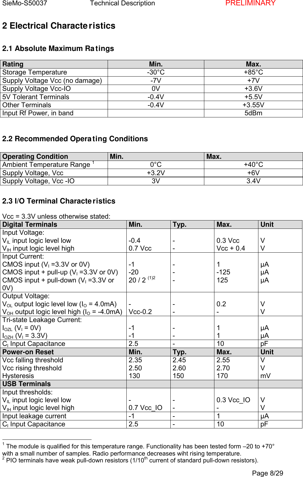
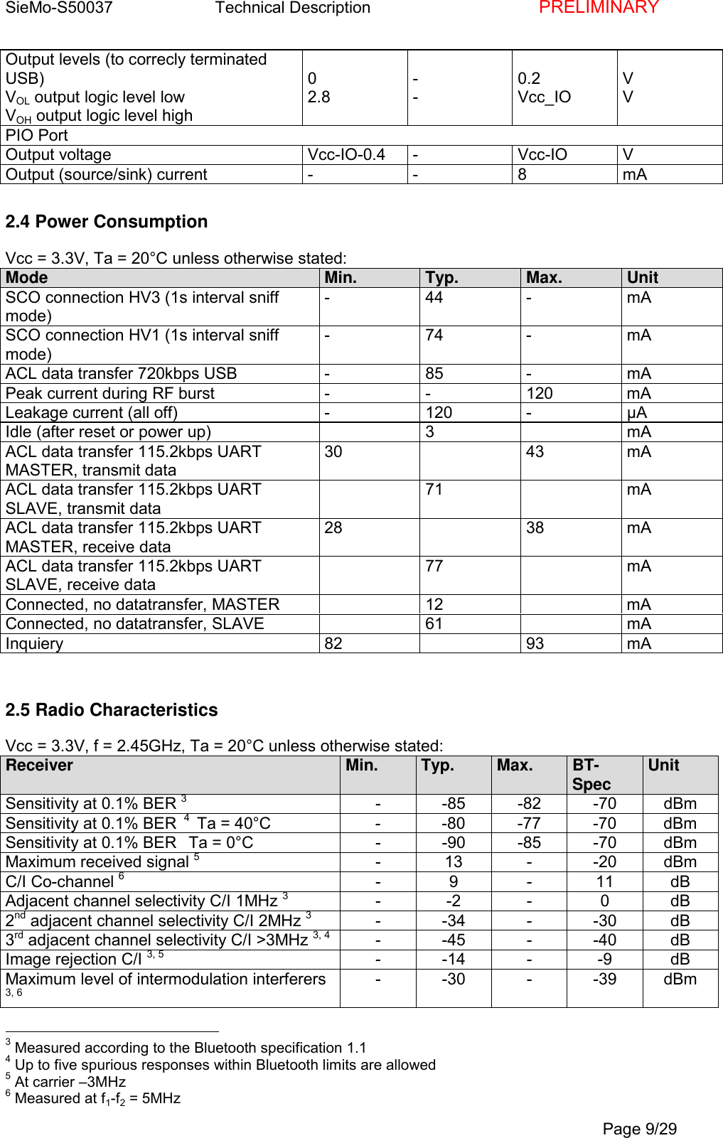
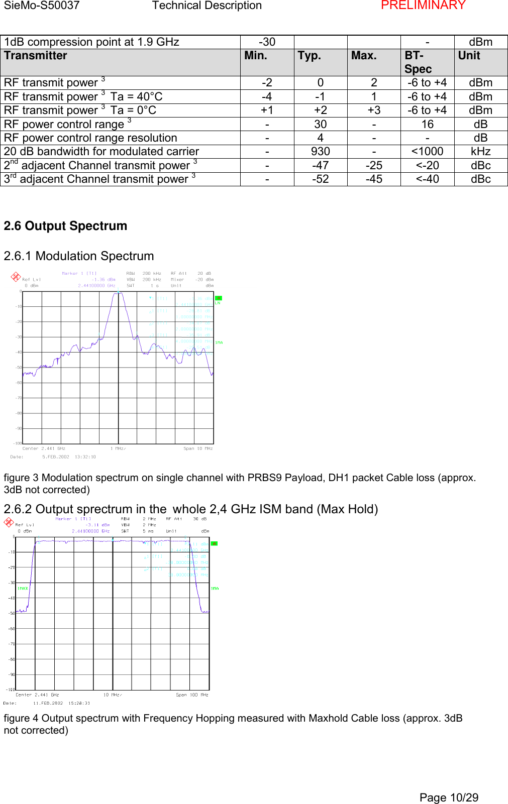
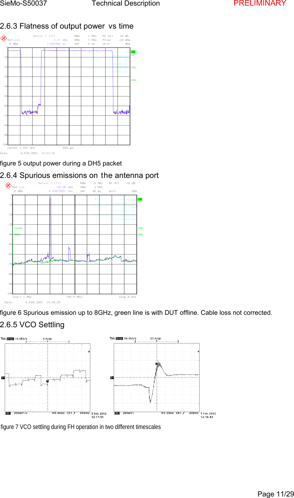
Contents
- 1. Reference Antenna description
- 2. Technical description
- 3. Test board description
Technical description
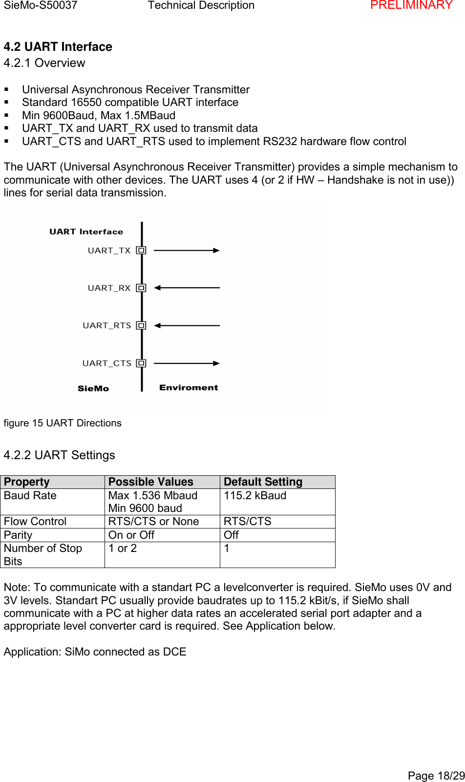
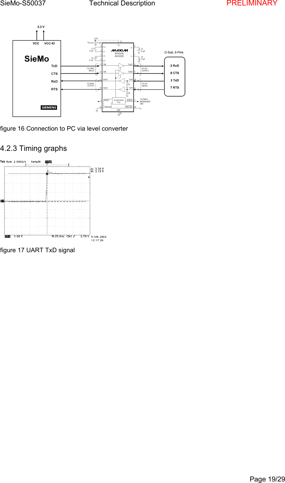
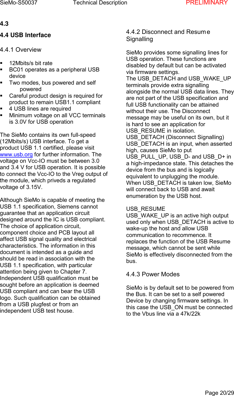
![SieMo-S50037 Technical Description PRELIMINARYPage 5/290 General Information0.1 HistoryIssue Date Reason for Changes01 2002-02-12 Initial issue02 2002-02-25 Redesign of document structure, inserting of the Clause RegulatoryStatementsTable 1: History0.2 References[1] http://www.bluetooth.com](https://usermanual.wiki/Siemens-Austria/SIEMO-S50037.Technical-description/User-Guide-230586-Page-5.png)
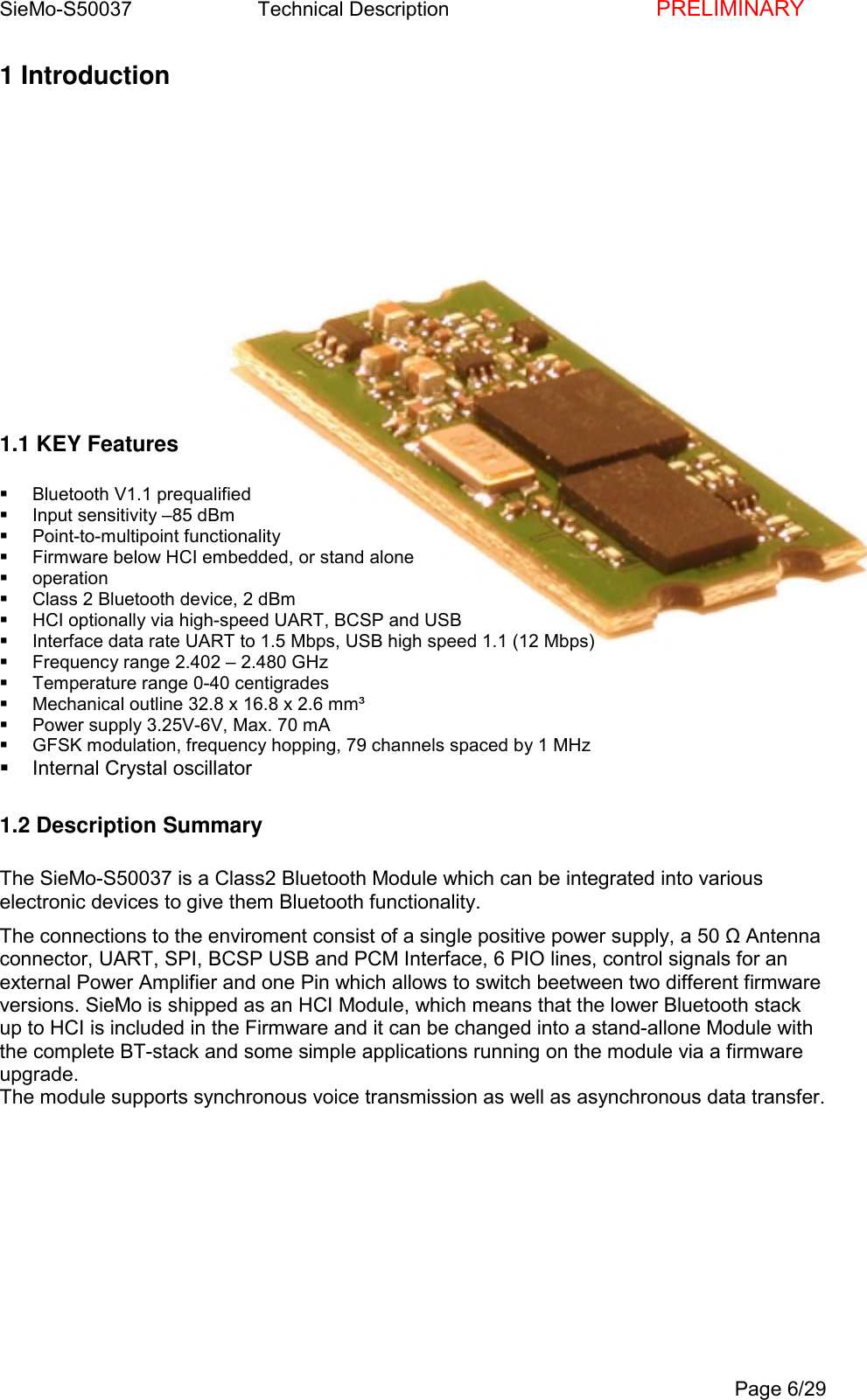
![SieMo-S50037 Technical Description PRELIMINARYPage 13/293 Pin Description3.1 Pinout Diagramfigure 10 SieMo Pinout, bottom view3.2 Pin description tablePin Name Type Pin DescriptionRFANT Rf in/out T2 Antenna output, 50Ω; unconditionallystable; DC path to GNDTX-EN CMOS output,pulled downF5 Control output for external switch or PARX-EN CMOS outputpulled downF4 Control output for external switch or LNATX-PWR Analog output F6 Ramping control output for external PA,need not be used, ramping is done on themodule.PowerVcc Power C6 Power Supply 3,25-6VVcc-IO Power C4 Power Supply for all IO-Pins, 3.0-3.4VUART-InterfaceTxD CMOS output, 5Vtolerant, pulled downB5 UART data outputRxD CMOS input, 5Vtolerant, pulled downA5 UART data inputRTS CMOS output A6 UART Ready To SendCTS CMOS input B6 UART Clear To SendUSB-InterfaceD+ CMOS bidirectional B1 USB D+D- CMOS bidirectional B2 USB D-USB_PULL_UP/PIO[2]CMOS bidirectional,pulled downD1 USB Pull-up, internally attached to D+, onlyused with corresponding USB-settings.USB_WAKE_UP/PIO[3]CMOS bidirectional,pulled downB4 Output goes high to wake up PC when inUSB mode, only used with corresponding USB-settings.USB_ON/PIO[4]CMOS bidirectional,pulled downD2 USB On (Input. Senses when VBUS is highwakes SieMo), only used with corresponding USB-](https://usermanual.wiki/Siemens-Austria/SIEMO-S50037.Technical-description/User-Guide-230586-Page-13.png)
![SieMo-S50037 Technical Description PRELIMINARYPage 14/29settings.USB_DETACH/PIO[5]CMOS bidirectional,pulled downC1 Chip detaches from USB when this line ishigh, only used with corresponding USB-settings.PCM-InterfacePCM_IN CMOS inputpulled downA1 Synchronous 8kss-1data inputPCM_OUT CMOS outputpulled downA2 Synchronous 8kss-1data outputPCM_SYNC CMOS bidirectional,pulled downA3 Synchronous data strobePCM_CLK CMOS bidirectional,pulled downA4 Synchronous data clockSPI-InterfaceSPI-CSB CMOS input, 5Vtolerant, pulled upE1 SPI Chip SelectSPI-CLK CMOS input, 5Vtolerant, pulled downE2 SPI ClockSPI-MOSI CMOS input, 5Vtolerant, pulled upE3 SPI Data InputSPI-MISO CMOS output,tristateE4 SPI Data OutputPIO-InterfacePIO[2]/USB_PULL_UPCMOS bidirectional,pulled downD1 Programmable IO linePIO[3]/USB_WAKE_UPCMOS bidirectional,pulled downB4 Programmable IO linePIO[4]/USB_ON CMOS bidirectional,pulled downD2 Programmable IO linePIO[5]/USB_DETACHCMOS bidirectional,pulled downC1 Programmable IO linePIO[6]/ CMOS bidirectional,pulled downD5 Programmable IO linePIO[7]/ CMOS bidirectional,pulled downD6 Programmable IO lineSpecial FunctionsRESET# CMOS inputpulled upR3 Reset# inputSCAN_ENABLE CMOS inputpulled downF1 For Test only, do not connectMODE CMOS inputpulled downD3 Selects second Firmware, if programmed](https://usermanual.wiki/Siemens-Austria/SIEMO-S50037.Technical-description/User-Guide-230586-Page-14.png)
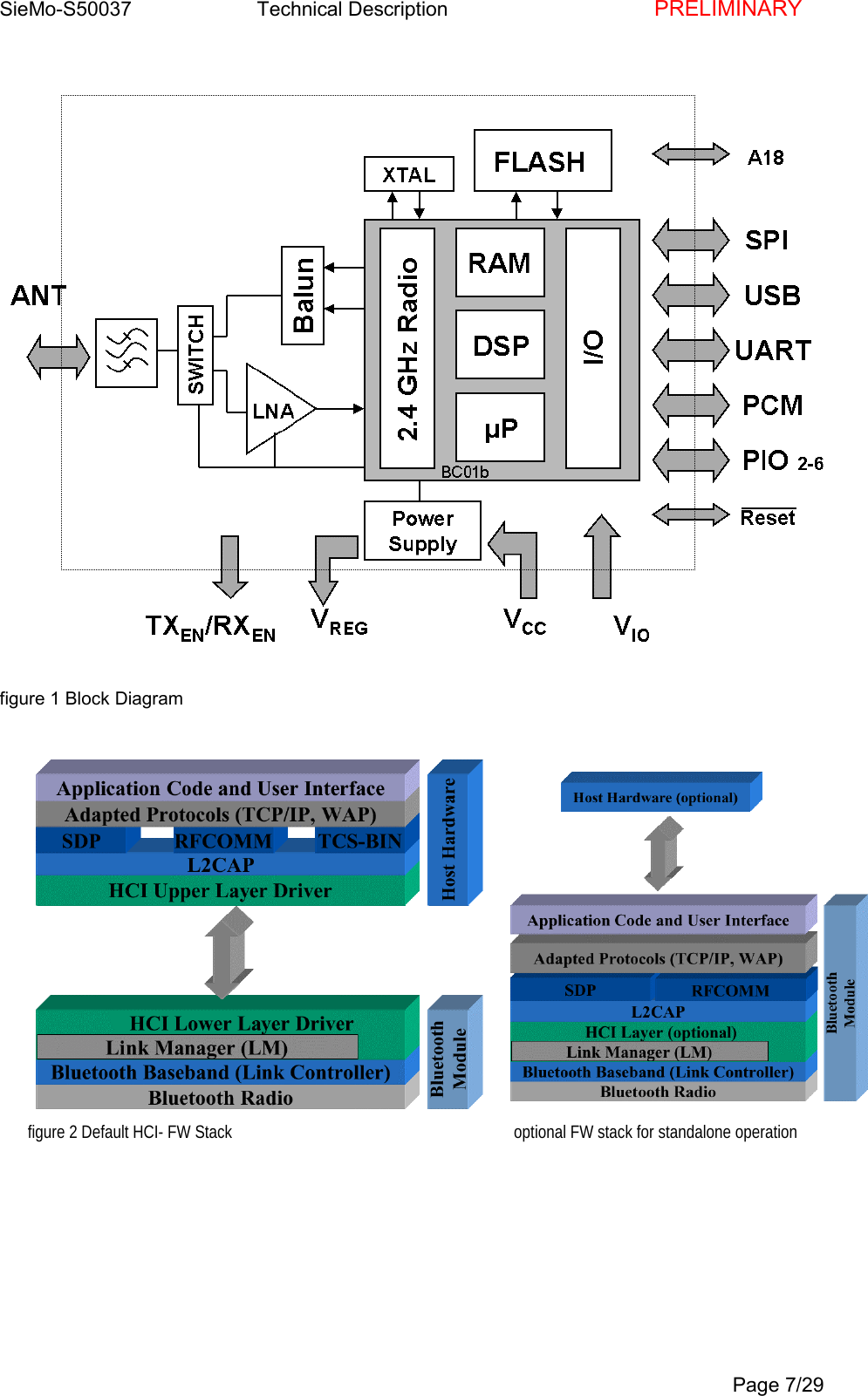
![SieMo-S50037 Technical Description PRELIMINARYPage 22/294.5.3 Single-Cycle OperationAfter a serial peripheral interface transaction finishes, the master toggles SPI_CLK withSPI_CSB high to initiate a new transaction. SPI_CSB must be high for at least two SPI_CLKcycles.4.5.4 Multi-Slave OperationSieMo should not be connected in a multi-slave arrangement by simple parallel connection ofslave MISO lines. When SieMo is deselected (SPI_CSB = 1), the SPI_MISO line does notfloat. Instead, SieMo outputs 0 if the processor is running or 1 if it is stopped.4.5.5 Writing to SieMoTo write to the SieMo, the 8-bit write command (00000010) is sent first (C[7:0] followed by a16-bit address (A[15:0]). 16 bits of data (D:[15:0]) are sent.Terminal Type Description DeviceTerminal PC ParallelConnectorSPI_CSB CMOS input Serial Peripheral Interface ChipSelectE1 2SPI_CLK CMOS input Serial Peripheral Interface SPIClockE2 9SPI_MOSI CMOS input Serial Peripheral Interface SPIData InputE3 8SPI_MISO CMOS output Serial Peripheral Interface SPIData OutputE4 10GND B3 194.5.6 SPI Timingfigure 20 SPI write operation a](https://usermanual.wiki/Siemens-Austria/SIEMO-S50037.Technical-description/User-Guide-230586-Page-22.png)
![SieMo-S50037 Technical Description PRELIMINARYPage 23/29figure 21 SPI write operation b4.5.7 Reading from SieMoReading is similar to writing, in that an 8-bit read command (00000011) is sent first, followedby the address of the location to be read. The SieMo then outputs the 16-bit contents of thelocation on MISO during bits D[15:0] and a check-word during T[15:0].The check-word iscomposed of {command, address [15:8]}. The check-word may be used to 'sanity-check' aread operation to a memory location. This overcomes the problem encountered with typicalserial peripheral interface slaves, whereby it is impossible to determine whether the datareturned by a read operation is valid data, or the result ofthe slave device not responding.figure 22 SPI read timing afigure 23 SPI read timing b](https://usermanual.wiki/Siemens-Austria/SIEMO-S50037.Technical-description/User-Guide-230586-Page-23.png)