Siemens Austria SIEMO-S50037 Bluetooth Module SieMo-S50037 User Manual SieMo S50037
Siemens AG Austria Bluetooth Module SieMo-S50037 SieMo S50037
Contents
- 1. Reference Antenna description
- 2. Technical description
- 3. Test board description
Technical description

SieMo-S50037 Technical Description PRELIMINARY
Page 1/29
Technical Description
Siemens Bluetooth™ Module
SieMo-S50037
S50037-Q5-*
Issued by
Program and System Engineering
Product and Solutions
Radio Communication Devices
Erdberger Laende 26, A-1031 Vienna, Austria
Copyright Siemens AG 2002 All Rights Reserved.
SIEMENS AKTIENGESELLSCHAFT

File Name: SieMo_S50037 Technical Description.doc Page 2/29
Author Part of this Document Department
Canbolant D. Regulatory Statements, Bluetooth™ Trademark PSE PRO RCD 3
Jatschka T. Technical Clauses PSE PRO RCD 3
3/29
0 General Information ................................................................................................. 5
0.1 History.......................................................................................................................... 5
0.2 References................................................................................................................... 5
1 Introduction .............................................................................................................. 6
1.1 KEY Features............................................................................................................... 6
1.2 Description Summary ................................................................................................... 6
2 Electrical Characteristics.......................................................................................... 8
2.1 Absolute Maximum Ratings.......................................................................................... 8
2.2 Recommended Operating Conditions........................................................................... 8
2.3 I/O Terminal Characteristics......................................................................................... 8
2.4 Power Consumption..................................................................................................... 9
2.5 Radio Characteristics ................................................................................................... 9
2.6 Output Spectrum ........................................................................................................ 10
2.6.1 Modulation Spectrum................................................................................................10
2.6.2 Output sprectrum in the whole 2,4 GHz ISM band (Max Hold) ..................................10
2.6.3 Flatness of output power vs time ..............................................................................11
2.6.4 Spurious emissions on the antenna port ...................................................................11
VCO Settling......................................................................................................................11
2.6.6 S-Parameter of the Antenna port ..............................................................................12
3 Pin Description....................................................................................................... 13
3.1 Pinout Diagram .......................................................................................................... 13
3.2 Pin description table................................................................................................... 13
4 Interface Description.............................................................................................. 15
4.1 PCM Interface ............................................................................................................ 15
4.1.1 Overview...................................................................................................................15
4.1.2 Description................................................................................................................15
4.1.3 Generic PCM Interface .............................................................................................15
4.1.4 PCM Timing..............................................................................................................16
Timing graphs....................................................................................................................17
4.2 UART Interface .......................................................................................................... 18
4.2.1 Overview...................................................................................................................18
4.2.2 UART Settings..........................................................................................................18
4.2.3 Timing graphs...........................................................................................................19
4.4 USB Interface............................................................................................................. 20
4.4.1 Overview...................................................................................................................20
4.4.2 Disconnect and Resume Signalling...........................................................................20
4.4.3 Power Modes............................................................................................................20
4.4.4 USB Timing ..............................................................................................................21
4.5 Serial Peripheral Interface.......................................................................................... 21
4.5.1 Overview...................................................................................................................21
4.5.2 Instruction Cycle .......................................................................................................21
4.5.3 Single-Cycle Operation.............................................................................................22
4.5.4 Multi-Slave Operation ...............................................................................................22
4.5.5 Writing to SieMo .......................................................................................................22
4.5.6 SPI Timing ................................................................................................................22
4.5.7 Reading from SieMo .................................................................................................23
4.5.8 Auto-Increment Operation.........................................................................................24
5 Functional Description ........................................................................................... 25
4/29
6 Regulatory Statements .......................................................................................... 26
6.1 General ...................................................................................................................... 26
6.2 European Union (EU) and EFTA Member States ....................................................... 26
6.3 United States of America (USA) ................................................................................. 27
7 Bluetooth Trademark ............................................................................................. 29

SieMo-S50037 Technical Description PRELIMINARY
Page 6/29
1 Introduction
1.1 KEY Features
Bluetooth V1.1 prequalified
Input sensitivity –85 dBm
Point-to-multipoint functionality
Firmware below HCI embedded, or stand alone
operation
Class 2 Bluetooth device, 2 dBm
HCI optionally via high-speed UART, BCSP and USB
Interface data rate UART to 1.5 Mbps, USB high speed 1.1 (12 Mbps)
Frequency range 2.402 – 2.480 GHz
Temperature range 0-40 centigrades
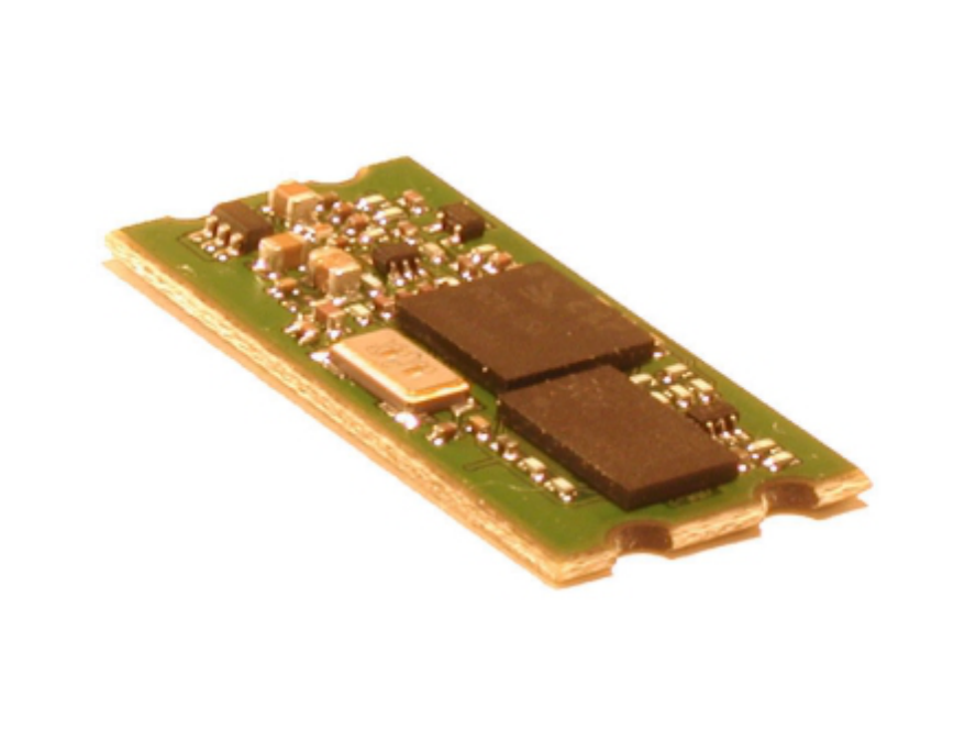
Mechanical outline 32.8 x 16.8 x 2.6 mm³
Power supply 3.25V-6V, Max. 70 mA
GFSK modulation, frequency hopping, 79 channels spaced by 1 MHz
Internal Crystal oscillator
1.2 Description Summary
The SieMo-S50037 is a Class2 Bluetooth Module which can be integrated into various
electronic devices to give them Bluetooth functionality.
The connections to the enviroment consist of a single positive power supply, a 50 Ω Antenna
connector, UART, SPI, BCSP USB and PCM Interface, 6 PIO lines, control signals for an
external Power Amplifier and one Pin which allows to switch beetween two different firmware
versions. SieMo is shipped as an HCI Module, which means that the lower Bluetooth stack
up to HCI is included in the Firmware and it can be changed into a stand-allone Module with
the complete BT-stack and some simple applications running on the module via a firmware
upgrade.
The module supports synchronous voice transmission as well as asynchronous data transfer.
SieMo-S50037 Technical Description PRELIMINARY
Page 7/29
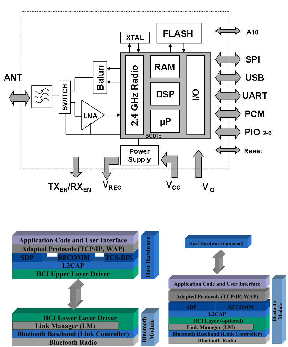
figure 1 Block Diagram
figure 2 Default HCI- FW Stack optional FW stack for standalone operation

SieMo-S50037 Technical Description PRELIMINARY
Page 8/29
2 Electrical Characteristics
2.1 Absolute Maximum Ratings
Rating Min. Max.
Storage Temperature -30°C +85°C
Supply Voltage Vcc (no damage) -7V +7V
Supply Voltage Vcc-IO 0V +3.6V
5V Tolerant Terminals -0.4V +5.5V
Other Terminals -0.4V +3.55V
Input Rf Power, in band 5dBm
2.2 Recommended Operating Conditions
Operating Condition Min. Max.
Ambient Temperature Range 10°C +40°C
Supply Voltage, Vcc +3.2V +6V
Supply Voltage, Vcc -IO 3V 3.4V
2.3 I/O Terminal Characteristics
Vcc = 3.3V unless otherwise stated:
Digital Terminals Min. Typ. Max. Unit
Input Voltage:
VIL input logic level low
VIH input logic level high
-0.4
0.7 Vcc
-
-
0.3 Vcc
Vcc + 0.4
V
V
Input Current:
CMOS input (VI =3.3V or 0V)
CMOS input + pull-up (VI =3.3V or 0V)
CMOS input + pull-down (VI =3.3V or
0V)
-1
-20
20 / 2 (1)2
-
-
-
1
-125
125
µA
µA
µA
Output Voltage:
VOL output logic level low (IO = 4.0mA)
VOH output logic level high (IO = -4.0mA)
-
Vcc-0.2
-
-
0.2
-
V
V
Tri-state Leakage Current:
IOZL (VI = 0V)
IOZH (VI = 3.3V)
-1
-1
-
-
1
1
µA
µA
CI Input Capacitance 2.5 - 10 pF
Power-on Reset Min. Typ. Max. Unit
Vcc falling threshold
Vcc rising threshold
Hysteresis
2.35
2.50
130
2.45
2.60
150
2.55
2.70
170
V
V
mV
USB Terminals
Input thresholds:
VIL input logic level low
VIH input logic level high
-
0.7 Vcc_IO
-
-
0.3 Vcc_IO
-
V
V
Input leakage current -1 - 1 µA
CI Input Capacitance 2.5 - 10 pF
1 The module is qualified for this temperature range. Functionality has been tested form –20 to +70°
with a small number of samples. Radio performance decreases wiht rising temperature.
2 PIO terminals have weak pull-down resistors (1/10th current of standard pull-down resistors).

SieMo-S50037 Technical Description PRELIMINARY
Page 9/29
Output levels (to correcly terminated
USB)
VOL output logic level low
VOH output logic level high
0
2.8
-
-
0.2
Vcc_IO
V
V
PIO Port
Output voltage Vcc-IO-0.4 - Vcc-IO V
Output (source/sink) current - - 8 mA
2.4 Power Consumption
Vcc = 3.3V, Ta = 20°C unless otherwise stated:
Mode Min. Typ. Max. Unit
SCO connection HV3 (1s interval sniff
mode)
-44-mA
SCO connection HV1 (1s interval sniff
mode)
-74-mA
ACL data transfer 720kbps USB - 85 - mA
Peak current during RF burst - - 120 mA
Leakage current (all off) - 120 - µA
Idle (after reset or power up) 3 mA
ACL data transfer 115.2kbps UART
MASTER, transmit data
30 43 mA
ACL data transfer 115.2kbps UART
SLAVE, transmit data
71 mA
ACL data transfer 115.2kbps UART
MASTER, receive data
28 38 mA
ACL data transfer 115.2kbps UART
SLAVE, receive data
77 mA
Connected, no datatransfer, MASTER 12 mA
Connected, no datatransfer, SLAVE 61 mA
Inquiery 82 93 mA
2.5 Radio Characteristics
Vcc = 3.3V, f = 2.45GHz, Ta = 20°C unless otherwise stated:
Receiver Min. Typ. Max. BT-
Spec Unit
Sensitivity at 0.1% BER 3- -85 -82 -70 dBm
Sensitivity at 0.1% BER 4 Ta = 40°C - -80 -77 -70 dBm
Sensitivity at 0.1% BER Ta = 0°C - -90 -85 -70 dBm
Maximum received signal 5-13--20dBm
C/I Co-channel 6-9-11dB
Adjacent channel selectivity C/I 1MHz 3--2- 0dB
2nd adjacent channel selectivity C/I 2MHz 3- -34 - -30 dB
3rd adjacent channel selectivity C/I >3MHz 3, 4 - -45 - -40 dB
Image rejection C/I 3, 5 --14- -9dB
Maximum level of intermodulation interferers
3, 6
- -30 - -39 dBm
3 Measured according to the Bluetooth specification 1.1
4 Up to five spurious responses within Bluetooth limits are allowed
5 At carrier –3MHz
6 Measured at f1-f2 = 5MHz
SieMo-S50037 Technical Description PRELIMINARY
Page 10/29
1dB compression point at 1.9 GHz -30 - dBm
Transmitter Min. Typ. Max. BT-
Spec Unit
RF transmit power 3-2 0 2 -6 to +4 dBm
RF transmit power 3 Ta = 40°C -4 -1 1 -6 to +4 dBm
RF transmit power 3 Ta = 0°C +1 +2 +3 -6 to +4 dBm
RF power control range 3- 30 - 16 dB
RF power control range resolution - 4 - - dB
20 dB bandwidth for modulated carrier - 930 - <1000 kHz
2nd adjacent Channel transmit power 3--47-25<-20dBc
3rd adjacent Channel transmit power 3--52-45<-40dBc
2.6 Output Spectrum
2.6.1 Modulation Spectrum
figure 3 Modulation spectrum on single channel with PRBS9 Payload, DH1 packet Cable loss (approx.
3dB not corrected)
2.6.2 Output sprectrum in the whole 2,4 GHz ISM band (Max Hold)
figure 4 Output spectrum with Frequency Hopping measured with Maxhold Cable loss (approx. 3dB
not corrected)
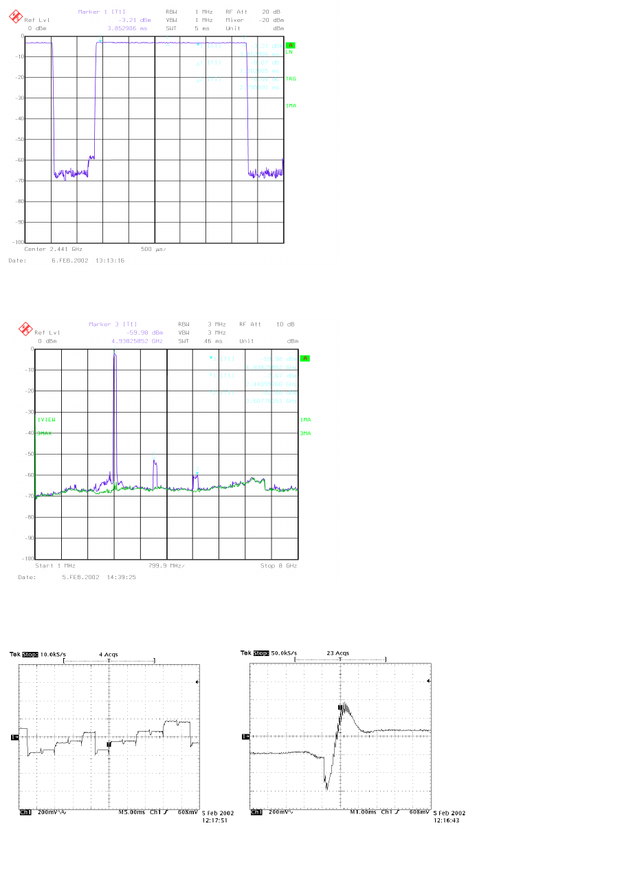
SieMo-S50037 Technical Description PRELIMINARY
Page 11/29
2.6.3 Flatness of output power vs time
figure 5 output power during a DH5 packet
2.6.4 Spurious emissions on the antenna port
figure 6 Spurious emission up to 8GHz, green line is with DUT offline. Cable loss not corrected.
2.6.5 VCO Settling
figure 7 VCO settling during FH operation in two different timescales
SieMo-S50037 Technical Description PRELIMINARY
Page 12/29
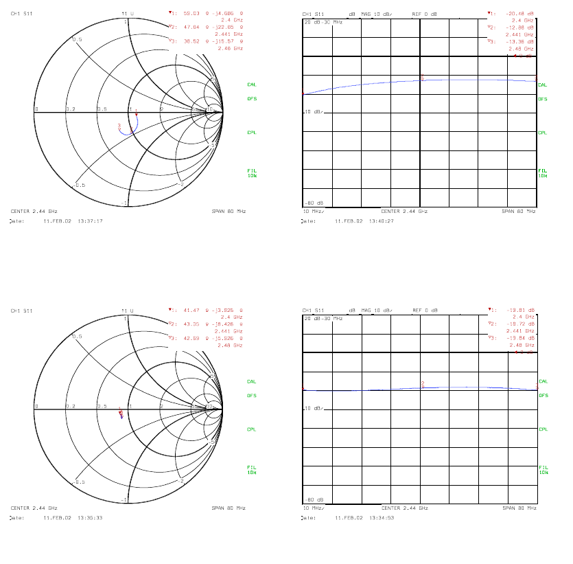
2.6.6 S-Parameter of the Antenna port
figure 8 S11 on the antenna port in transmit mode
figure 9 S11 on the antenna port in receive mode
SieMo-S50037 Technical Description PRELIMINARY
Page 13/29
3 Pin Description
3.1 Pinout Diagram
figure 10 SieMo Pinout, bottom view
3.2 Pin description table
Pin Name Type Pin Description
RF
ANT Rf in/out T2 Antenna output, 50Ω; unconditionally
stable; DC path to GND
TX-EN CMOS output,
pulled down
F5 Control output for external switch or PA
RX-EN CMOS output
pulled down
F4 Control output for external switch or LNA
TX-PWR Analog output F6 Ramping control output for external PA,
need not be used, ramping is done on the
module.
Power
Vcc Power C6 Power Supply 3,25-6V
Vcc-IO Power C4 Power Supply for all IO-Pins, 3.0-3.4V
UART-Interface
TxD CMOS output, 5V
tolerant, pulled down
B5 UART data output
RxD CMOS input, 5V
tolerant, pulled down
A5 UART data input
RTS CMOS output A6 UART Ready To Send
CTS CMOS input B6 UART Clear To Send
USB-Interface
D+ CMOS bidirectional B1 USB D+
D- CMOS bidirectional B2 USB D-
USB_PULL_UP
/PIO[2]
CMOS bidirectional,
pulled down
D1 USB Pull-up, internally attached to D+, only
used with corresponding USB-settings.
USB_WAKE_U
P/PIO[3]
CMOS bidirectional,
pulled down
B4 Output goes high to wake up PC when in
USB mode, only used with corresponding USB-settings.
USB_ON/
PIO[4]
CMOS bidirectional,
pulled down
D2 USB On (Input. Senses when VBUS is high
wakes SieMo), only used with corresponding USB-

SieMo-S50037 Technical Description PRELIMINARY
Page 14/29
settings.
USB_DETACH/
PIO[5]
CMOS bidirectional,
pulled down
C1 Chip detaches from USB when this line is
high, only used with corresponding USB-settings.
PCM-Interface
PCM_IN CMOS input
pulled down
A1 Synchronous 8kss-1data input
PCM_OUT CMOS output
pulled down
A2 Synchronous 8kss-1data output
PCM_SYNC CMOS bidirectional,
pulled down
A3 Synchronous data strobe
PCM_CLK CMOS bidirectional,
pulled down
A4 Synchronous data clock
SPI-Interface
SPI-CSB CMOS input, 5V
tolerant, pulled up
E1 SPI Chip Select
SPI-CLK CMOS input, 5V
tolerant, pulled down
E2 SPI Clock
SPI-MOSI CMOS input, 5V
tolerant, pulled up
E3 SPI Data Input
SPI-MISO CMOS output,
tristate
E4 SPI Data Output
PIO-Interface
PIO[2]/USB_PULL
_UP
CMOS bidirectional,
pulled down
D1 Programmable IO line
PIO[3]/USB_WAK
E_UP
CMOS bidirectional,
pulled down
B4 Programmable IO line
PIO[4]/USB_ON CMOS bidirectional,
pulled down
D2 Programmable IO line
PIO[5]/USB_DETA
CH
CMOS bidirectional,
pulled down
C1 Programmable IO line
PIO[6]/ CMOS bidirectional,
pulled down
D5 Programmable IO line
PIO[7]/ CMOS bidirectional,
pulled down
D6 Programmable IO line
Special Functions
RESET# CMOS input
pulled up
R3 Reset# input
SCAN_ENABLE CMOS input
pulled down
F1 For Test only, do not connect
MODE CMOS input
pulled down
D3 Selects second Firmware, if programmed
SieMo-S50037 Technical Description PRELIMINARY
Page 15/29
4 Interface Description
4.1 PCM Interface
4.1.1 Overview
PCM Pulse Code Modulation is a
standard method used to digitise
human voice
Four-wire, full duplex serial interface
used to transfer a single voice channel
to an external audio codec
Maximum of one SCO connection is
possible using the PCM interface
Further SCO channels must use the
HCI protocol layer
Data format is 13 bit linear PCM
4.1.2 Description
Pulse Code Modulation (PCM) is the
standard method used to digitise human
voice patterns for transmission over digital
communication channels. Through its
PCM interface, SieMo provides hardware
support for continual transmission and
reception of PCM data, thus reducing
processor overhead for wireless headset
applications.
SieMo offers a bi-directional digital audio
interface that routes directly into the
baseband layer of the on-chip firmware (it
does not pass through the HCI
protocollayer). Hardware on SieMo allows
the data to be sent to and received from a
SCO connection. Only one SCO
connection can be supported by the PCM
interface at any one time. Any additional
SCO connections must receive and
transmit their data over the HCI protocol
layer. The data format is 13-bit linear
PCM. SieMo can operate either as a
master (with an output clock of 256kHz) or
as a slave (with the input clock varying
between 128kHz and 512kHz). When in
slave mode and using higher clock rates
SieMo can support Motorola's
Synchronous Serial Interface (SSI)
standard that allows multiple bi-directional
audio channels to be multiplexed onto a
single physical connection.
4.1.3 Generic PCM Interface
For a generic PCM interface there is one
master and one slave device. The master
generates the clock and synchronisation
signals. The sync signal identifies the start
of the sample data and has an 8kHz
period. There are two types of frame sync:
long andshort. In long frame sync mode
PCM_SYNC going high indicates the first
(and most significant) bit of the sample. It
must remain high for at least two clock
cycles, but this can be longer. In short
frame sync MSB start is signalled by sync
going low (normally it only goes high for
one clock cycle).
The clock runs at a higher rate than sync:
at least 8 x bits_per_sample MHz,
although higher rates are common. The
sample resolution is 13 bits/sample,
uncompressed. Several Motorola
CODECs allow their output gain to be
controlled via the addition of three extra
data bits after the audio data. SieMo
supports this feature, effectively raising the
bits per sample to 16. Data from both the
master and slave is clocked out on the
rising clock edge and sampled on the
falling edge. Master mode is the default
setting. In master mode SieMo generates
a 256kHz clock signal (PCM_CLK) and the
8kHz, long format synchronisation signal
(PCM_SYNC). Short frame sync is not
supported. See PCM Timing Diagrams for
more information.
Slave mode is selected by setting a
Persistent Store value. In slave mode
SieMo clocks output data on the rising
edge of the received clock signal and
samples incoming data on the falling edge.
The incoming clock frequency should be
between 128kHz and 512kHz. (Note that
128kHz is 8 x 16 kHz, therefore the
absolute minimum possible frequency for
the 8ksamples/sec and 16bits/sample (13
audio data plus three gain data). The
frame sync must be long format. Short
format is not supported (see SSI Mode
and Timing Diagrams in this section for
moreinformation).
SieMo-S50037 Technical Description PRELIMINARY
Page 16/29
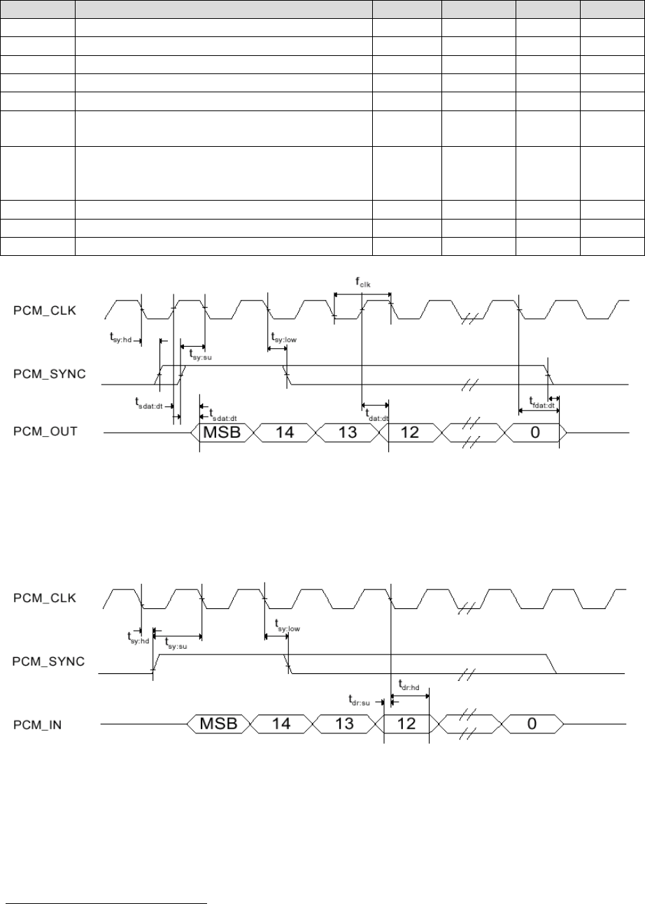
4.1.4 PCM Timing
Symbol Parameter Min Typ Max Unit
fCLK PCM clock frequency 256 kHz
(1) Clock duty cycle 50 %
tsy:hd Hold time from CLK low to SYNC high 1.95 us
tsy:su Set-up time for SYNC high to CLK low 1.95 us
tsdat:dt Delay time from CLK to valid MSB data 50 ns
tdat:dt Delay time from CLK high to PCM_OUT
valid data
50 ns
tfdat:dt Delay time from SYNC or CLK, whichever
is later, to PCM_OUT data line high
impedance
3007ns
tsy:low Hold time from 2nd CLK to SYNC low 3001ns
tdr:su Set-up time for PCM_IN valid to CLK low 3001ns
tdr:hd Hold time for CLK low to PCM_IN invalid 3001ns
figure 11 PCM Master Timing
7 Assumes normal system clock operation. Figures may vary during low power modes
when system clock speeds are reduced.
SieMo-S50037 Technical Description PRELIMINARY
Page 17/29
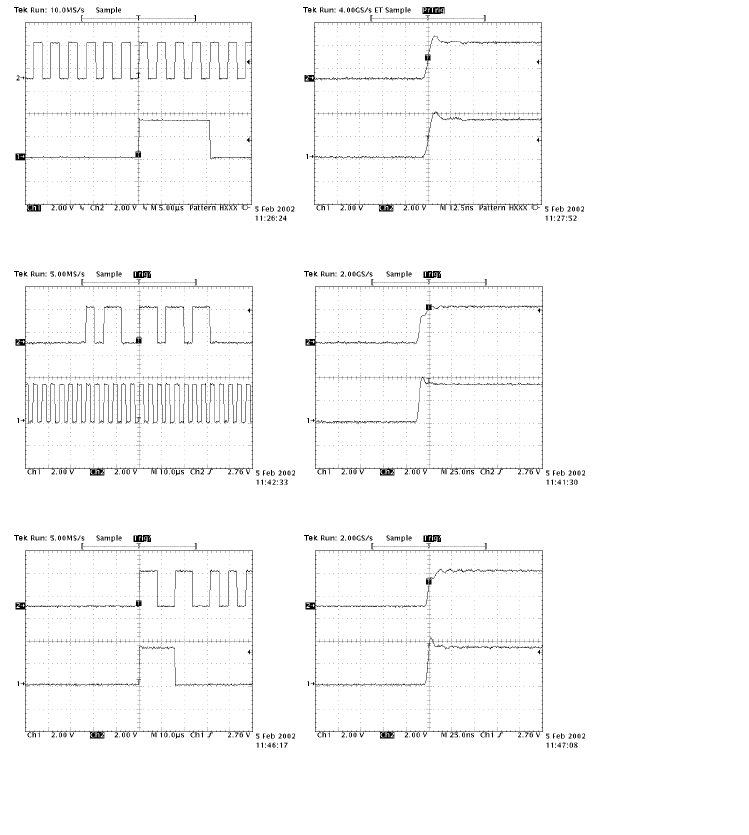
4.1.5 Timing graphs
figure 14 PCM clock (upper) vs PCM sync in 2 different Timescales
figure 14 PCM OUT vs PCM CLOCK in two different timescales
figure 14 PCM OUT vs PCM SYNC in two different timescales
SieMo-S50037 Technical Description PRELIMINARY
Page 18/29
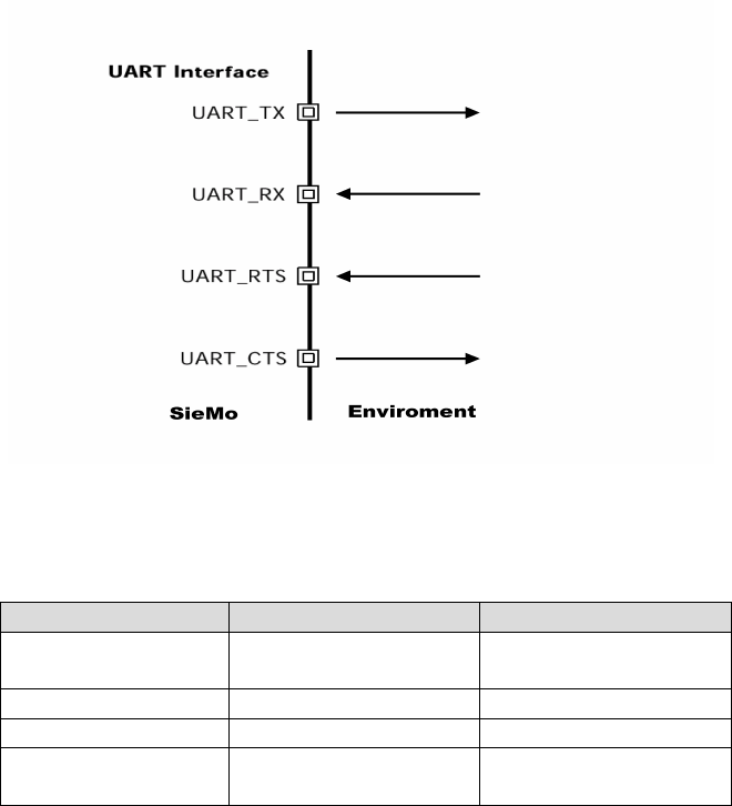
4.2 UART Interface
4.2.1 Overview
Universal Asynchronous Receiver Transmitter
Standard 16550 compatible UART interface
Min 9600Baud, Max 1.5MBaud
UART_TX and UART_RX used to transmit data
UART_CTS and UART_RTS used to implement RS232 hardware flow control
The UART (Universal Asynchronous Receiver Transmitter) provides a simple mechanism to
communicate with other devices. The UART uses 4 (or 2 if HW – Handshake is not in use))
lines for serial data transmission.
figure 15 UART Directions
4.2.2 UART Settings
Property Possible Values Default Setting
Baud Rate Max 1.536 Mbaud
Min 9600 baud
115.2 kBaud
Flow Control RTS/CTS or None RTS/CTS
Parity On or Off Off
Number of Stop
Bits
1 or 2 1
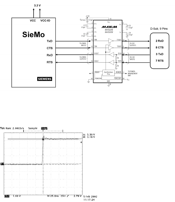
Note: To communicate with a standart PC a levelconverter is required. SieMo uses 0V and
3V levels. Standart PC usually provide baudrates up to 115.2 kBit/s, if SieMo shall
communicate with a PC at higher data rates an accelerated serial port adapter and a
appropriate level converter card is required. See Application below.
Application: SiMo connected as DCE
SieMo-S50037 Technical Description PRELIMINARY
Page 19/29
figure 16 Connection to PC via level converter
4.2.3 Timing graphs
figure 17 UART TxD signal

SieMo-S50037 Technical Description PRELIMINARY
Page 20/29
4.3
4.4 USB Interface
4.4.1 Overview
12Mbits/s bit rate
BC01 operates as a peripheral USB
device
Two modes, bus powered and self
powered
Careful product design is required for
product to remain USB1.1 compliant
4 USB lines are required
Minimum voltage on all VCC terminals
is 3.0V for USB operation
The SieMo contains its own full-speed
(12Mbits/s) USB interface. To get a
product USB 1.1 certified, please visit
www.usb.org for further information. The
voltage on Vcc-IO must be between 3.0
and 3.4 V for USB operation. It is possible
to connect the Vcc-IO to the Vreg output of
the module, which priveds a regulated
voltage of 3.15V.
Although SieMo is capable of meeting the
USB 1.1 specification, Siemens cannot
guarantee that an application circuit
designed around the IC is USB compliant.
The choice of application circuit,
component choice and PCB layout all
affect USB signal quality and electrical
characteristics. The information in this
document is intended as a guide and
should be read in association with the
USB 1.1 specification, with particular
attention being given to Chapter 7.
Independent USB qualification must be
sought before an application is deemed
USB compliant and can bear the USB
logo. Such qualification can be obtained
from a USB plugfest or from an
independent USB test house.
4.4.2 Disconnect and Resum e
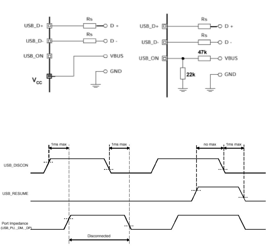
Signalling
SieMo provides some signalling lines for
USB operation. These functions are
disabled by default but can be activated
via firmware settings.
The USB_DETACH and USB_WAKE_UP
terminals provide extra signalling
alongside the normal USB data lines. They
are not part of the USB specification and
full USB functionality can be attained
without their use. The Disconnect
message may be useful on its own, but it
is hard to see an application for
USB_RESUME in isolation.
USB_DETACH (Disconnect Signalling)
USB_DETACH is an input, when asserted
high, causes SieMo to put
USB_PULL_UP, USB_D- and USB_D+ in
a high-impedance state. This detaches the
device from the bus and is logically
equivalent to unplugging the module.
When USB_DETACH is taken low, SieMo
will connect back to USB and await
enumeration by the USB host.
USB_RESUME
USB_WAKE_UP is an active high output
used only when USB_DETACH is active to
wake-up the host and allow USB
communication to recommence. It
replaces the function of the USB Resume
message, which cannot be sent while
SieMo is effectively disconnected from the
bus.
4.4.3 Power Modes
SieMo is by default set to be powered from
the Bus. It can be set to a self powered
Device by changing firmware settings. In
this case the USB_ON must be connected
to the Vbus line via a 47k/22k
SieMo-S50037 Technical Description PRELIMINARY
Page 21/29
figure 18 USB Power Modes- Applications
4.4.4 USB Timing
figure 19 USB Disconnect and Resume Signal Timing
4.5 Serial Peripheral Interface
4.5.1 Overview
Consistent with the Motorola SPI standard
SieMo always acts in slave mode
SPI_CLK is always generated by the host
SieMo uses 16-bit addresses and 16-bit data during serial peripheral interface transactions.
Such transactions will operate regardless of whether the internal processor is running or is
stopped. This section details the considerations required when interfacing to SieMo via the
four dedicated Serial peripheral interface terminals.
4.5.2 Instruction Cycle
Before SieMo can be addressed, SPI_CSB must be taken low (SPI_CSB = 0). Data on
SPI_MOSI is then clocked into the SieMo on the rising edge of the clockline SPI_CLK. When
reading, SieMo will reply to the master on MISO, the data being valid on the falling edge of
the SPI_CLK. The master provides the clocking.
SieMo-S50037 Technical Description PRELIMINARY
Page 22/29
4.5.3 Single-Cycle Operation
After a serial peripheral interface transaction finishes, the master toggles SPI_CLK with
SPI_CSB high to initiate a new transaction. SPI_CSB must be high for at least two SPI_CLK
cycles.
4.5.4 Multi-Slave Operation
SieMo should not be connected in a multi-slave arrangement by simple parallel connection of
slave MISO lines. When SieMo is deselected (SPI_CSB = 1), the SPI_MISO line does not
float. Instead, SieMo outputs 0 if the processor is running or 1 if it is stopped.
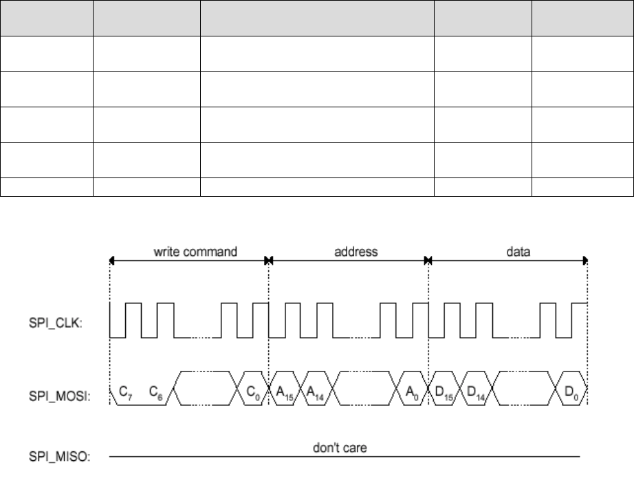
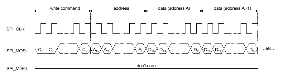
4.5.5 Writing to SieMo
To write to the SieMo, the 8-bit write command (00000010) is sent first (C[7:0] followed by a
16-bit address (A[15:0]). 16 bits of data (D:[15:0]) are sent.
Terminal Type Description Device
Terminal PC Parallel
Connector
SPI_CSB CMOS input Serial Peripheral Interface Chip
Select
E1 2
SPI_CLK CMOS input Serial Peripheral Interface SPI
Clock
E2 9
SPI_MOSI CMOS input Serial Peripheral Interface SPI
Data Input
E3 8
SPI_MISO CMOS output Serial Peripheral Interface SPI
Data Output
E4 10
GND B3 19
4.5.6 SPI Timing
figure 20 SPI write operation a
SieMo-S50037 Technical Description PRELIMINARY
Page 23/29
figure 21 SPI write operation b
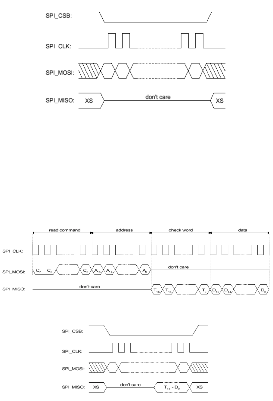
4.5.7 Reading from SieMo
Reading is similar to writing, in that an 8-bit read command (00000011) is sent first, followed
by the address of the location to be read. The SieMo then outputs the 16-bit contents of the
location on MISO during bits D[15:0] and a check-word during T[15:0].The check-word is
composed of {command, address [15:8]}. The check-word may be used to 'sanity-check' a
read operation to a memory location. This overcomes the problem encountered with typical
serial peripheral interface slaves, whereby it is impossible to determine whether the data
returned by a read operation is valid data, or the result ofthe slave device not responding.
figure 22 SPI read timing a
figure 23 SPI read timing b
SieMo-S50037 Technical Description PRELIMINARY
Page 24/29
4.5.8 Auto-Increment Operati on
Sending a command word and the address of a register every time it is to be read or written
can be a significant overhead, especially when large amounts of data are to be transferred.
SieMo offers increased data transfer efficiency via its auto-increment operation. During
operation, SieMo increments the address automatically. Only the data is transmitted or
received over the serial peripheral interface bus. SieMo keeps the previous command word.
figure 24 Example Auto-Increment Operation
SieMo-S50037 Technical Description PRELIMINARY
Page 25/29
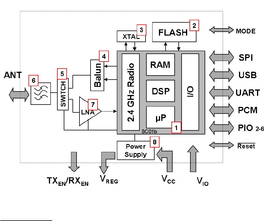
5 Functional Description
SieMo S50037 is a Bluetooth module which is consistent with Bluetooth specification 1.1.
The modules implimentation is based on the BC01b single chip by CSR Cambridge Silicon
Radio.
figure 25 block diagram
Functional Blocks:
1. BlueCore 01b (BC01b) CMOS-single chip bc Cambridge Silicon Radio (CSR)
2. 8 MBit Flash Memory
3. 13 MHz XTAL with asymmteric trimming capacitors, digitally trimmed during production.
Initial Tolerance <0.5 ppm, <20 ppm over age and temperature.
4. BALUN (BALanced to UNbalanced) performs transformation from symmetrical output to
assymetrical lines and biasing of the output stage.
5. Antenna switch switches between input and output direction to transmit or receive a
signal with TDM (Time Division Multiplex).
6. Output/Input Filter removes (out-of-band) spurious emissions and increases (out-of-band)
blocking performance.
7. LNA Low Noise Amplifier increases sensitivty of receiver and isolation between transmit
and reiceive path during transmission.
8. Power supply ensures that all rf-parameters fulfill the Bluetooth specification with an input
voltage range from 3.25 to 6V.
SieMo-S50037 Technical Description PRELIMINARY
Page 26/29
6 Regulatory Statements
6.1 General
• This Bluetooth radio module has to be installed and used in accordance with the
technical description/installation instructions provieded by the manufacturer.
• This Bluetooth radio module is intended to be placed on the market in all States, where
the BluetoothTM technologie and the used frequency band is released.
• For detail information concerning type approval of this module (eg. where this module is
already pre-approved) please contact the authorised local distributor or the manufacturer.
6.2 European Union (EU) and EFTA Member States
This Bluetooth module is an assessed radio module in conformity with the R&TTE directive
1999/5/EC and has been provided with the CE mark accordingly.
It is conform to the following specifications/Standards∗
∗∗
∗) :
Applied specifications/Standards Essential Requirement
(Corresponding article of R&TTE)
EN 300 328 (ETS 300 328): Part 1, V1.1.1 and
Part 2, V1.2.2 (2000-07)
EN 301 489-17 (ETS 300 826): V1.1.1 (2000-09)
Electromagnetic Compatibility
(Art. 3.1b)
EN 300 328 (ETS 300 328): Part 1, V1.1.1 and
Part 2, V1.2.2 (2000-07) Radio Frequency Spectrum Efficiency
(Art. 3.2)
Note that the radio frequency band used by this equipment is not harmonized throughout
the European Community. According to the R&TTE directive 1999/5/EC is this equipment
a ‘Class 2’ equipment and marked accordingly with the assigned Class Identifier.
CE Conformity Marking:
∗
∗∗
∗ ) Safety requirement according to the article 3.1a of R&TTE Directive are not applicable on this
Bluetooth radio module, since it is intended to be integrated in final products/applications.

SieMo-S50037 Technical Description PRELIMINARY
Page 27/29
Because this Bluetooth™ radio module is very small and intended to be integrated/installed
in final products (OEM products/applications) it is not practicable to place the label including
the CE conformity marking on it. Therefore the required labeling information is placed in this
technical description/installation manual of this radio module. However the CE conformity
marking reffered to in R&TTE Directiv, Article 12 is displayed on the packaging of the radio
module in an appropriate form.
OEM products/applications, where this Bluetooth™ radio module is integrated/installed in,
has to be labeled in accordance with R&TTE Directive, Article 12.
An auxiliary label is included in the packaging of this radio module, which can be used for
that purpose and has to be permanently affixed to the OEM product/application or to it`s data
plate and to it`s packaging and to accompanying documents. The label has to be affixed
visibly (label data must be visible from the outside of the equipment enclosure) legibly and
indelibly.
Note that in case of using the provieded auxiliary label, additionally following statement
has to be included in the users manual of the final product (OEM product/application):
Note that the radio frequency band used by this equipment is not harmonized throughout the
European Community. According to the R&TTE directive 1999/5/EC is this equipment
a ‘Class 2’ equipment and marked accordingly with the assigned Class Identifier.
6.3 United States of America (USA)
This Bluetooth radio module complies with part 15 of the Federal Communications
Commission (FCC) Rules and labeled in accordance with the FCC Rules.
FCC ID: P6L-SieMo-S50037
Operation is subject to the following two conditions:
(1) This device may not cause harmful interference, and
(2) this device must accept any interference received, including interference that may cause
undesired operation.
Note that any changes or modifications to this equipment not expressly approved by the
manufacturer could void the user’s authority to operate this equipment.
Because this Bluetooth™ radio module is very small and intended to be integrated/installed
in OEM products/applications it is not practicable to place the label including the FCC
statement on it. Therefore the required labeling information is placed in this capter of the
technical description/installation manual of this radio module. However the FCC identifier is
displayed on the packaging of the radio module in an appropriate form.
OEM products/applications, where this Bluetooth™ radio module is integrated/installed in,
has to be labeled in accordance with FCC Rules (section 15.19 and 47 CFR Ch. I: §2.925,
§2.926).
An auxiliary label is included in the packaging of this radio module, which can be used for
that purpose and has to be permanently affixed to the OEM product/application in a readily
visible (label data must be visible from the outside of the equipment enclosure) manner (eg.
on an exterior surface of the equipment).

SieMo-S50037 Technical Description PRELIMINARY
Page 28/29
Note that in case of using the provieded auxiliary label, additionally following statement
has to be included in the users manual of the final product (OEM product/application):
This device complies with part 15 of the Federal Communications Commission (FCC) Rules.
Operation is subject to the following two conditions:
(1) This device may not cause harmful interference, and
(2) this device must accept any interference received, including interference that may cause
undesired operation.
Note that any changes or modifications to this equipment not expressly approved by the
manufacturer could void the user’s authority to operate this equipment.
Manufacturer information concerning antenna:
The only antenna(s) approved for use with this Bluetooth™ radio module are those
documented in this construction file, and must be installed in the manner specified therein. In
all other cases, where the second manufacturer/installer desires to use an antenna with this
module that has not been previously approved for use with it, then one of the following
procedures has to be followed in order to ensure the compliance of the new antenna:
1. The Manufacturer of this Bluetooth radio module files a Class II permissive change to
approve the new antenna with the module.
2. The second manufacturer/installer obtains a separate FCC equipment authorization for
the module and the new antenna.
SieMo-S50037 Technical Description PRELIMINARY
Page 29/29
7 Bluetooth Trademark
BLUETOOTH is a trademark owned by Bluetooth SIG, Inc., U.S.A, and licensed to
Siemens AG.
This product is a qualified BluetoothTM product and compliant to the BluetoothTM
specifications version 1.1.