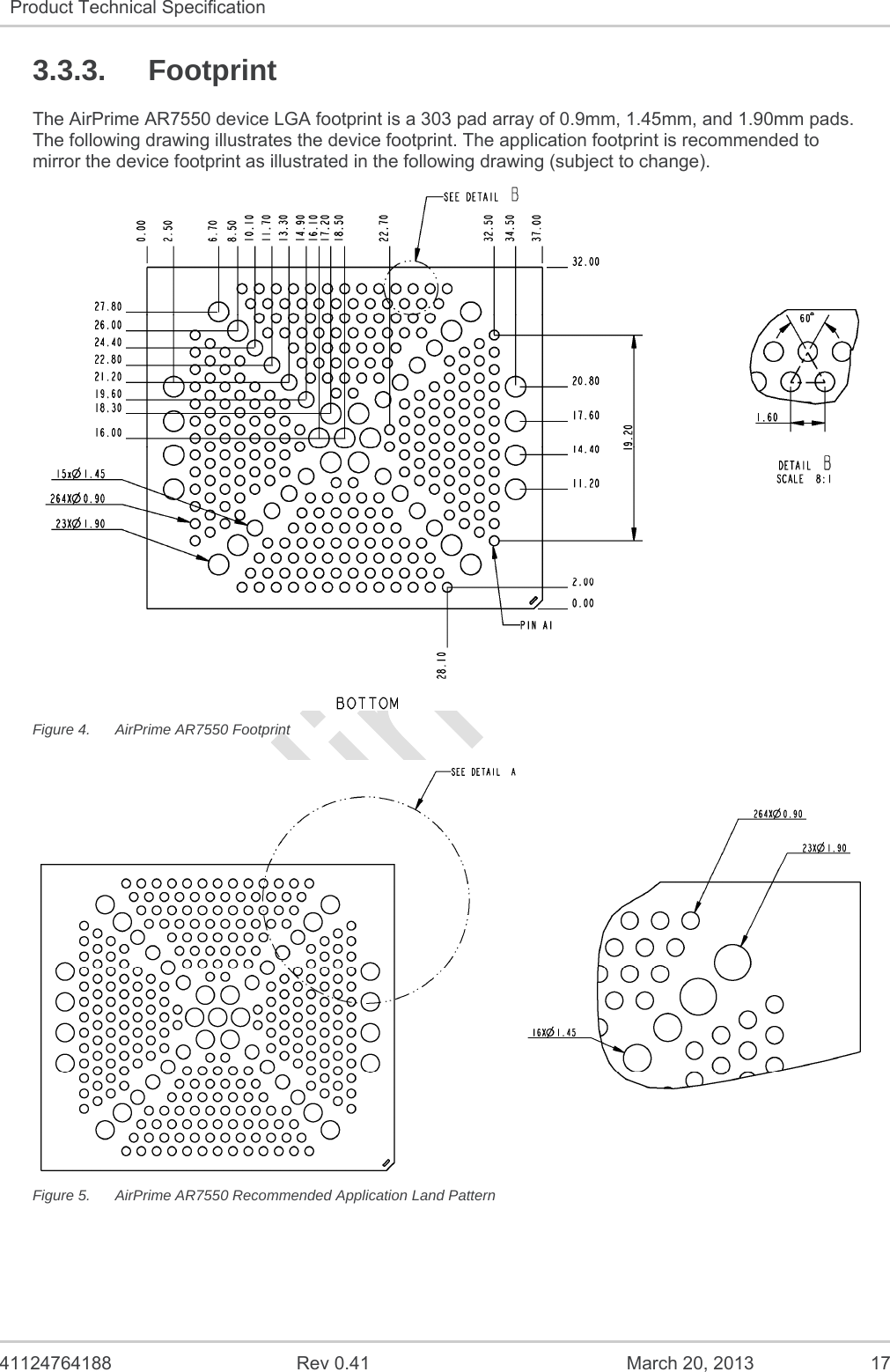
Sierra Wireless AR7550 Wireless Module User Manual AirPrime AR7550 Hardware Integration Guide Rev1 0bx
Sierra Wireless Inc. Wireless Module AirPrime AR7550 Hardware Integration Guide Rev1 0bx
AirPrime - AR7550 - Hardware Integration Guide - Rev1.0_v3

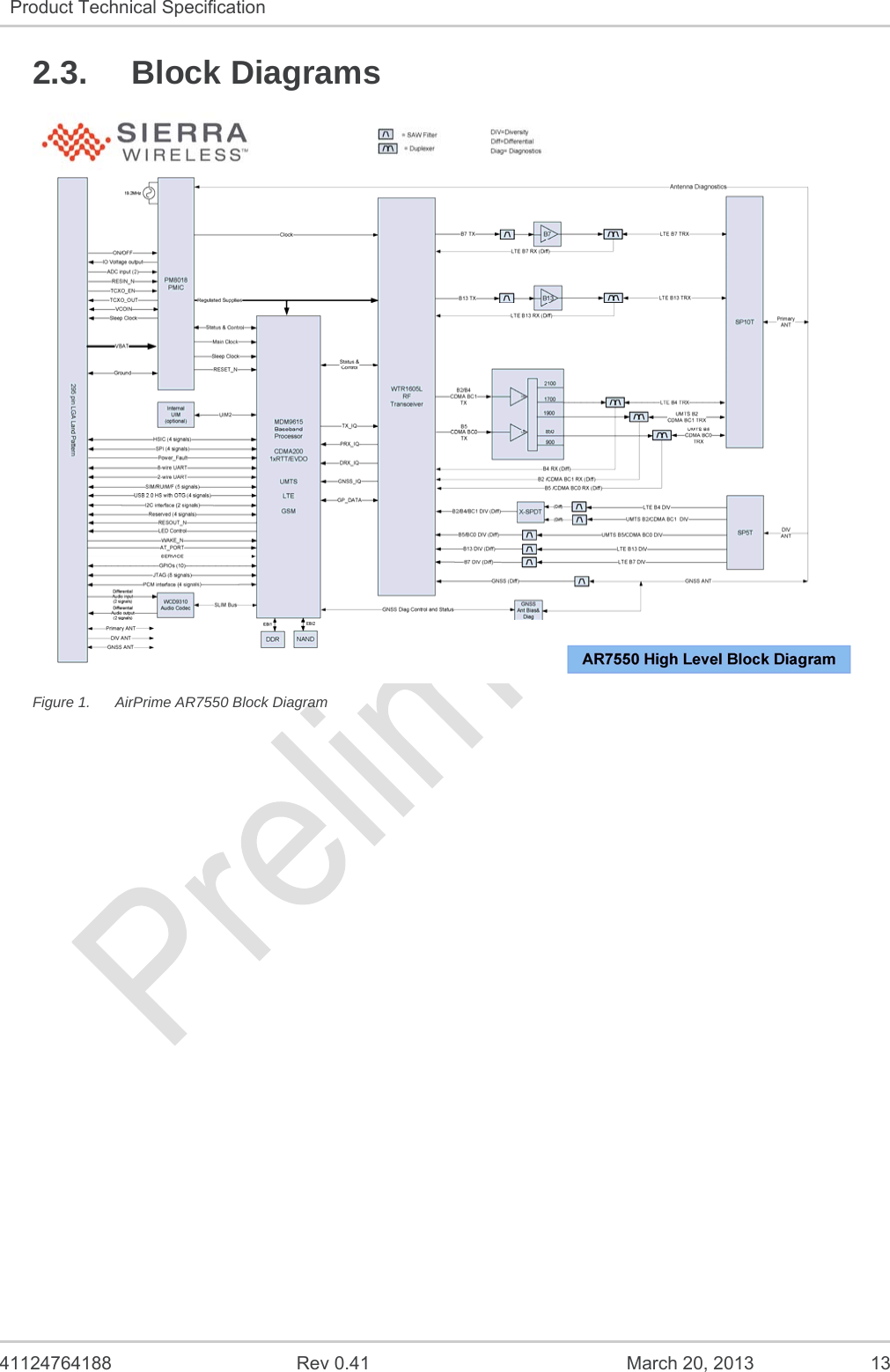
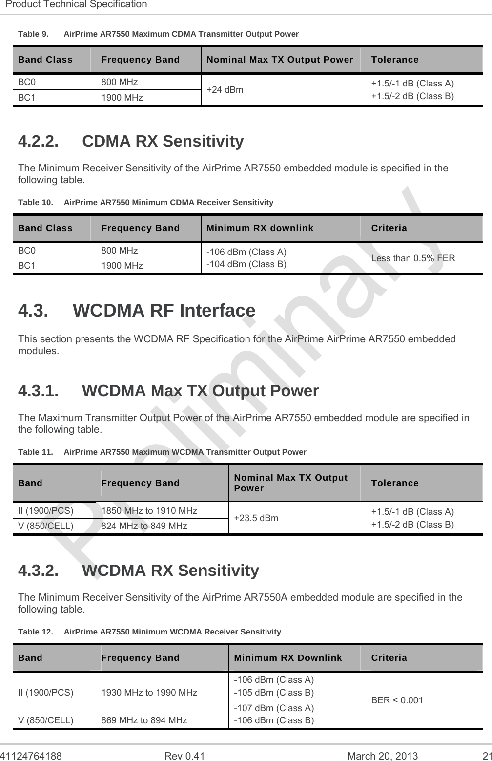
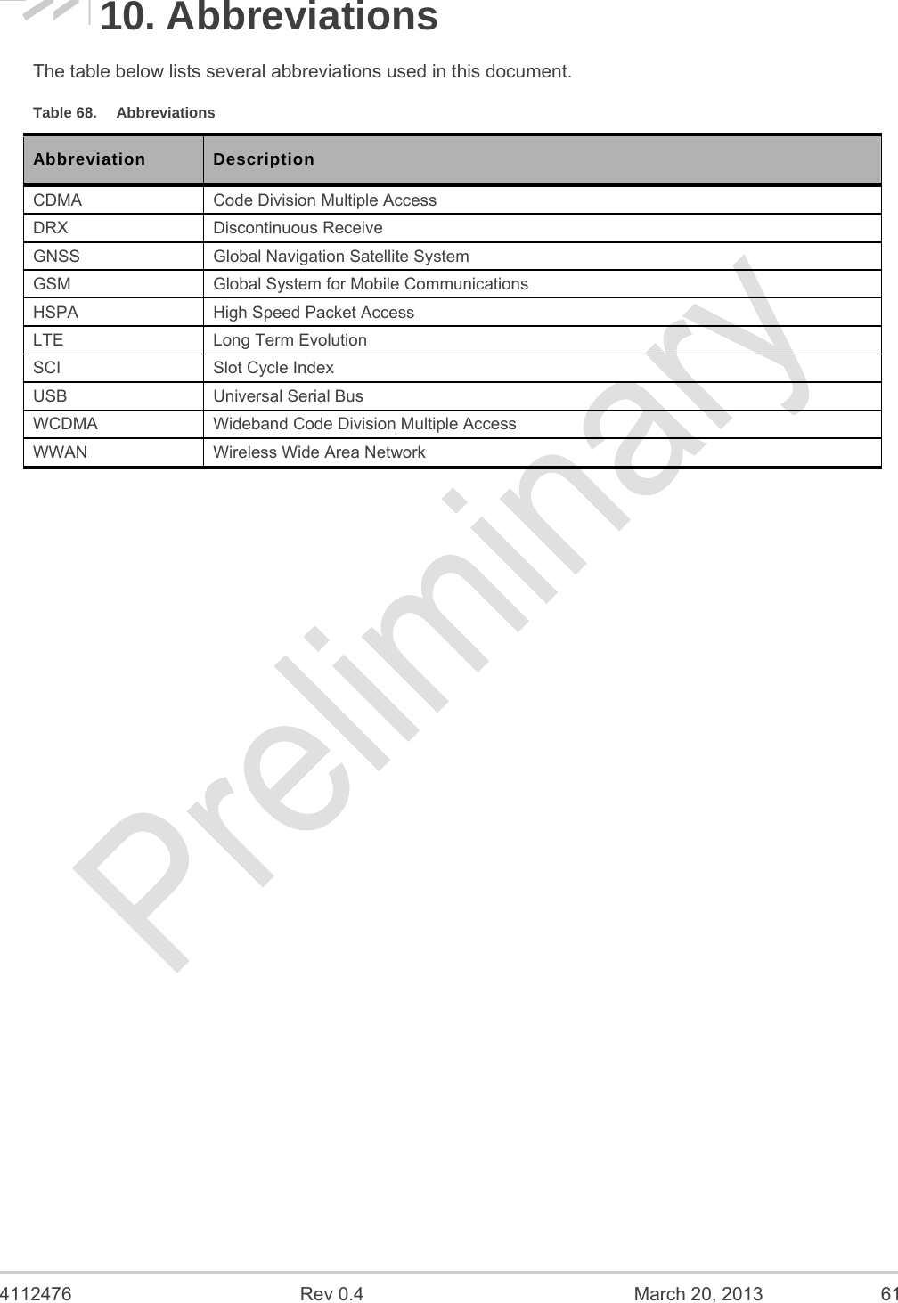
![41124764188 Rev 0.41 March 20, 2013 23 Product Technical Specification 4.5. Primary Antenna Diagnostics The primary antenna diagnostic feature allows the AirPrime AR7550 embedded module to determine if the primary antenna connected to the module is: open, shorted or normal. The antenna connected to this interface needs to have a DC resistance to ground of 10 k ± 1k embedded inside. The ARx55x FW accepts two limits which are used to evaluate the status of the antenna, representing the short and open thresholds. Refer to [7] for the syntax of AT+ANTLIMT. Table 16. Primary Antenna ADC Characteristics Min Nom Max Units ADC Voltage Range 0 0.9 1.8 Volts Resolution - 15 Bit ADC Values 0 16383 Voltage/ADC step ~0.0011 Volts 1 Assumes 10k Nominal DC resistance in the attached antenna and internal to AirPrime AR7550 device The following example illustrates the Antenna states and resistance values for a typical limit setting. AT+ANTLIMT=1,839,1088 Table 17. Primary Antenna Diagnostics Ranges Antenna State Min ADC Max ADC Antenna Resistance Range Short 0 839 ~ 7 k Normal 841 1086 7 k < x < 13 k Open 1088 1900 13 k Note: Highlighted numbers in the table above are programmed as shortLim and openLim using the +ANTLIMT command. 4.6. RX2 Antenna Diagnostics The RX2 antenna diagnostic feature allows the AirPrime AR75500 to determine if the RX2 antenna connected to the module is: open, shorted or normal. The antenna connected to this interface needs to have a DC resistance to ground of 10 k ± 1k embedded inside. The AirPrime AR7550 FW accepts two limits which are used to evaluate the status of the antenna, representing the short and open thresholds. Refer to [7] for the syntax of AT+ANTLIMT. Table 18. RX2 Antenna ADC Characteristics Min Nom Max Units ADC Voltage Range 0 0.9 1.8 Volts Resolution - 15 Bit ADC Values 0 16383 Voltage/ADC step ~0.0011 Volts 1 Assumes 10k Nominal DC resistance in the attached antenna and internal to AirPrime AR7550 device](https://usermanual.wiki/Sierra-Wireless/AR7550/User-Guide-1961582-Page-23.png)
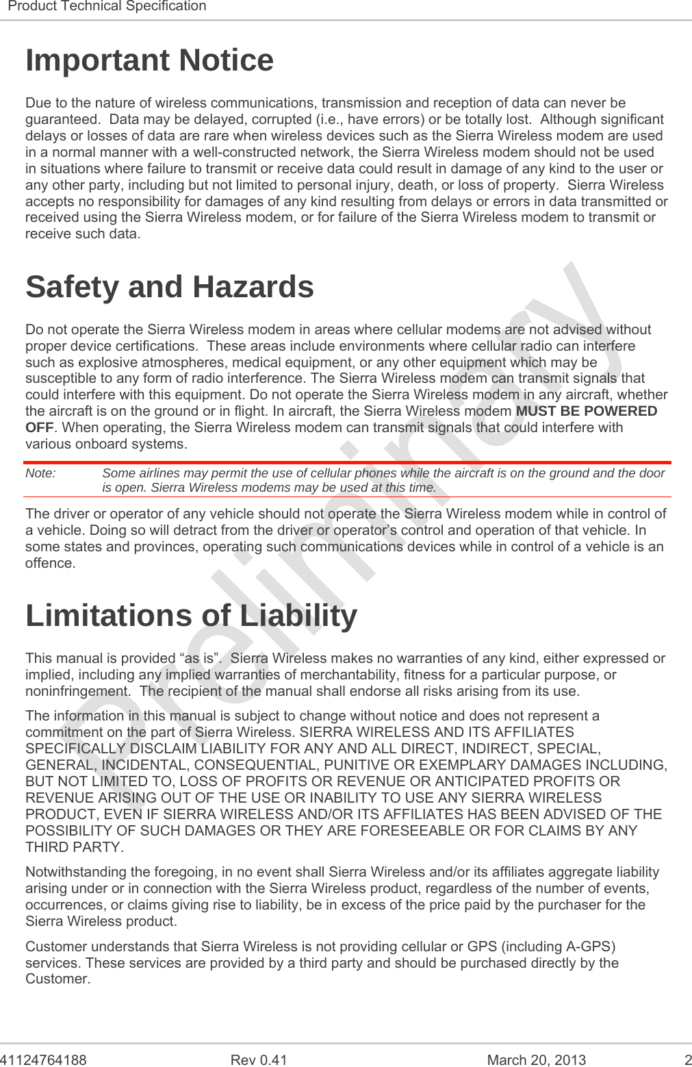
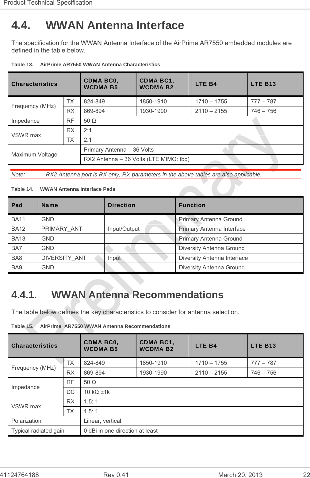
![41124764188 Rev 0.41 March 20, 2013 30 Product Technical Specification Parameter Comments Min Typ Max Units VIL Low level input voltage CMOS/Schmitt -0.3 – 0.35* VCC_1V8 V VOH High level output voltage CMOS, at pin rated drive strength VCC_1V8 - 0.45 – VCC_1V8 V VOL Low-level output voltage CMOS, at pin rated drive strength 0 – 0.45 V IOH High level output current VOH = VCC_1V8 – 0.45 V – – 6 mA IOL Low Level output current VOL = 0.45 V -6 – – mA IOH-LED High level output current LED signal only – – – mA IOL-LED Low Level output current LED signal only -3 – 20 mA IIHPD Input high leakage current With pull-down 5 30 µA IILPU Input low leakage current With pull-up -30 -5 µA IL Input leakage current VIO = max, VIN = 0 V to VIO LED signal only -0.3 – +0.35 µA CIN Input capacitance – – 7 pF CIN-LED Input capacitance LED signal only – – 5 pF Caution: Digital IOs shall not be pulled-up to an external voltage as this may cause VCC_1V8 to not go low when the AirPrime AR7550 device is powered down. Also, this would partially bias the AirPrime AR7550 device which could potentially damage the device or result in GPIOs being set to undetermined levels. 5.6. Internal Device Frequencies The table below summarizes the frequencies generated within the AirPrime AR7550. This table is provided for reference only to the device integrator. Table 28. Internal Device Frequencies Subsystem/Feature Frequency Units Real Time Clock 32.768 kHz PCM Audio interface (Primary PCM Master Mode) [TBD] 8, 128, 2048 kHz I2C Interface 400 kHz PMIC switching power supplies tbd MHz GNSS Antenna bias switching supply 3.5 MHz](https://usermanual.wiki/Sierra-Wireless/AR7550/User-Guide-1961582-Page-30.png)
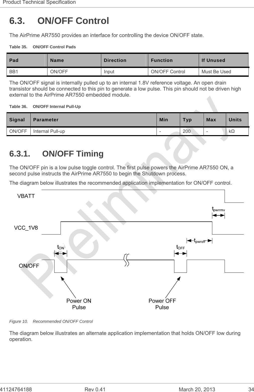
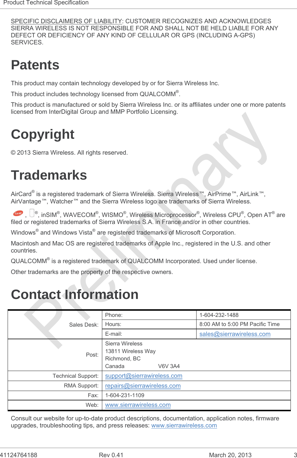
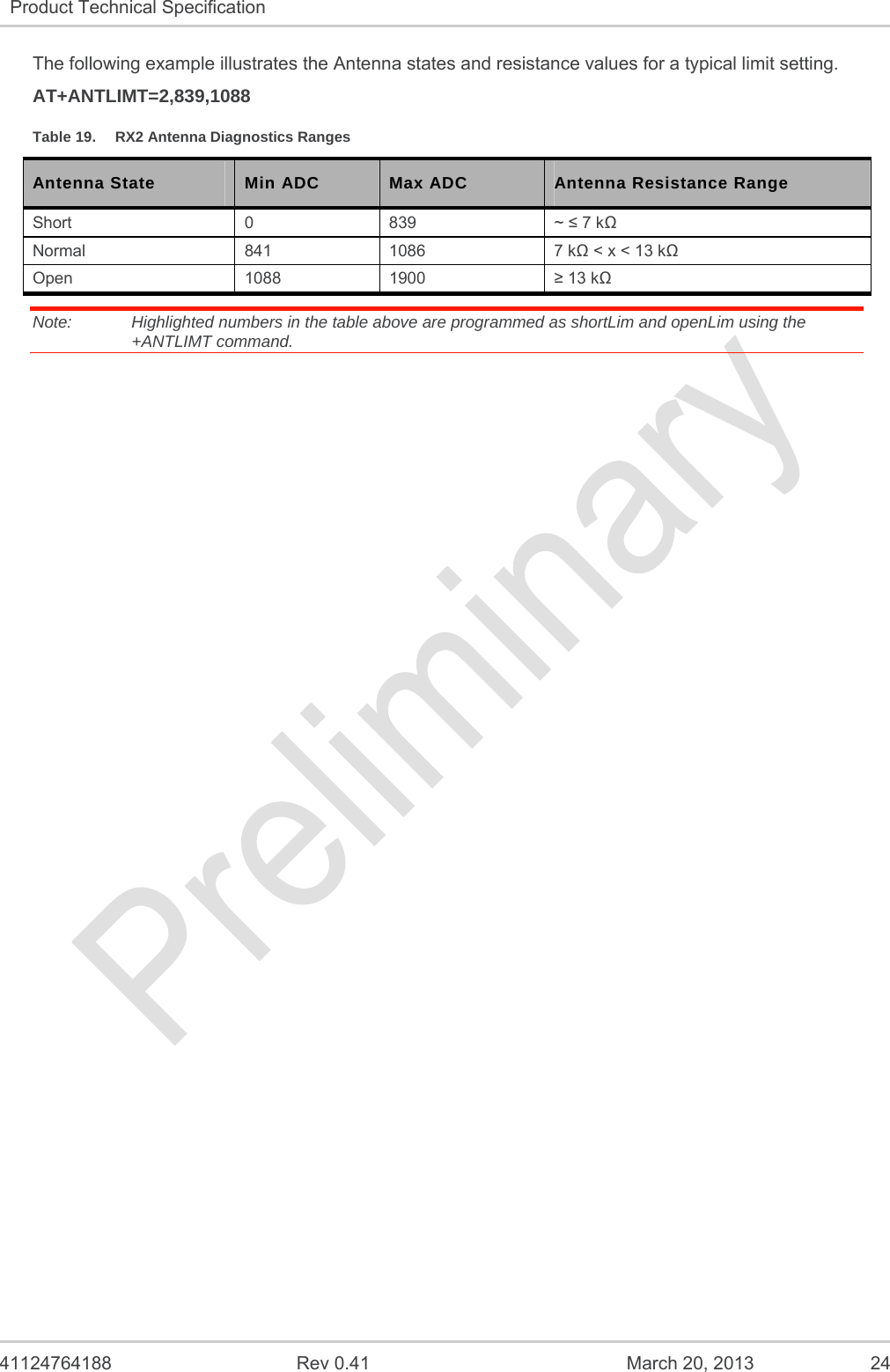
![41124764188 Rev 0.41 March 20, 2013 35 Product Technical Specification Figure 11. Alternate ON/OFF Control Table 37. Power-ON Sequence Symbol Definitions Symbol Parameter Boot Min Typ Max tON Turn ON Pulse duration 50 ms 100 ms tOFF Turn OFF Pulse duration 50 ms 100 ms 500 ms tpwroff Time to Power OFF - 5 s - tpwrrmv Time VBATT must be maintained after VCC_1V8 goes inactive 0 s - - tHI Time required for ON/OFF to be high prior to OFF pulse. In process 10 s - Complete 50 ms Tpwroff is the time between when a power OFF pulse is complete and when shutdown is completed by the AirPrime AR7550 devices. This duration is network and device dependent, i.e. in a CDMA network a power down registration is initiated by the AirPrime AR7550 device, when the acknowledgement is received from the network power OFF completes. Detection of power down can be accomplished by monitoring for one of the following: +WIND: 10 output on the AT Command interface USB ports are de-enumerated The application must wait for a power down to be detected prior to removing power from the AirPrime AR7550 device. If a timeout is required, it is recommended to be in excess of 30s prior to removing power from the AirPrime AR7550 device. Note: Refer to [7] for details on enabling the +WIND message for power down and +USLGRPMSK and +USLEVTMSK for unsolicited message output.](https://usermanual.wiki/Sierra-Wireless/AR7550/User-Guide-1961582-Page-35.png)
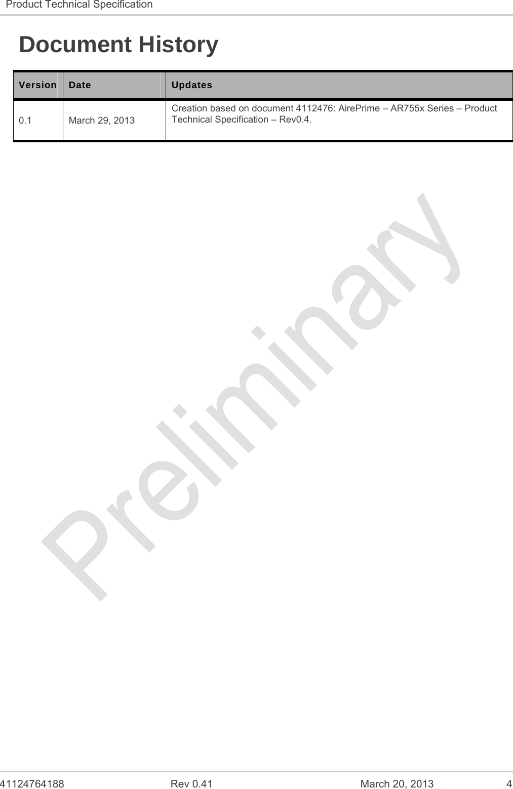
![41124764188 Rev 0.41 March 20, 2013 38 Product Technical Specification Table 41. USB Characteristics USB Value Units USB_VBUS Voltage range 2.0 – 5.25 V Maximum Current draw1 1 mA Maximum Input Capacitance (Min ESR = 50 m) 10 F 1 With the AirPrime AR7550 device powered ON. 6.5. UART The AirPrime AR7550 has two UART interfaces. The primary UART is an 8-wire1 electrical interface and the secondary UART is a 2-wire electrical interface. Table 42. UART Pads Pad Name Direction Function Interface If Unused AD9 RXD1 Output Receive Data (UART1) UART1 Leave Open AE6 RTS1 Input Ready To Send (UART1) UART1 Leave Open1 AD8 TXD1 Input Transmit Data (UART1) UART1 Leave Open AE7 CTS1 Output Clear To Send (UART1) UART1 Leave Open AF6 DCD1 Output Data Carrier Detect (UART1) UART1 Leave Open AE5 DTR1 Input Data Terminal Ready (UART1) UART1 Leave Open AF5 DSR1 Output Data Set Ready (UART1) UART1 Leave Open DB2 RXD2 Output UART2 Receive Data UART2 Leave Open DA2 TXD2 Input UART2 Transmit Data UART2 Leave Open 1 If UART1 is implemented as a 2-wire interface, RTS1 should be pulled low to disable flow control. 6.6. Ring Indicator The Ring Indicator (RI) may be used to notify an external application of several events such as an incoming call, timer expiration or incoming SMS. Table 43. Ring Indicator Pad Pad Name Direction Function If Unused AD7 RI1 Output Ring Indicator Leave Open The events which toggle the RI signal can be configured using the AT+WWAKESET command. The duration of the RI pulse can be configured using the AT+WRID command. The reason for the RI signal being activated can be queried using the AT+WWAKE command. Refer to [7] for details of these AT Commands. The RI signal is independent of the UART. 1 Includes Ring Indicator which may also be used independently of UART1.](https://usermanual.wiki/Sierra-Wireless/AR7550/User-Guide-1961582-Page-38.png)
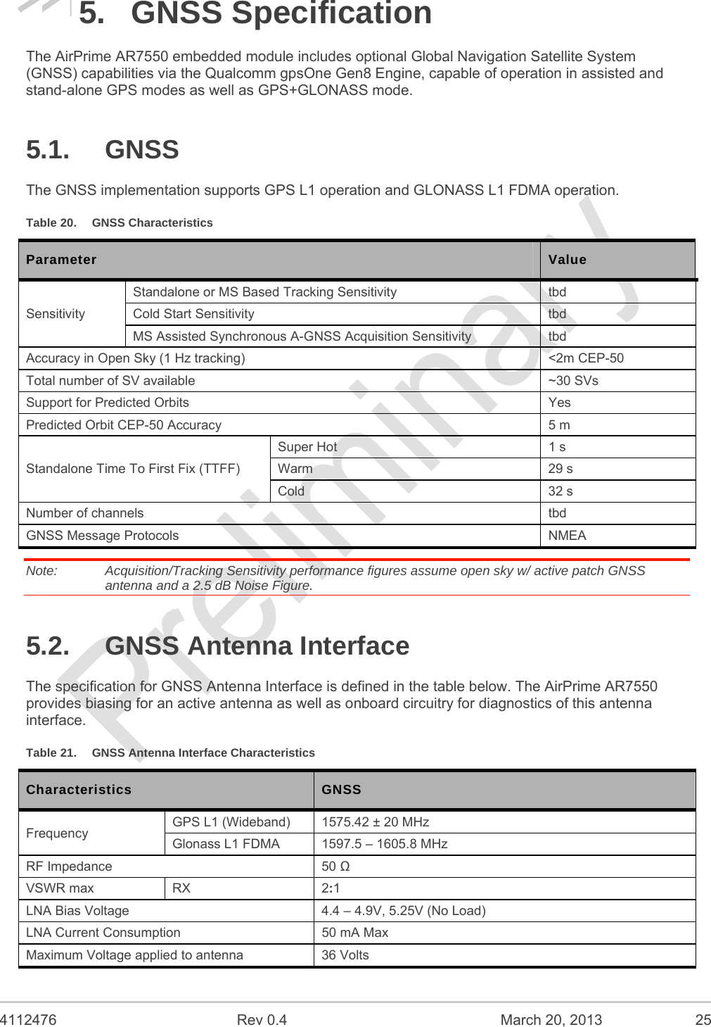
![41124764188 Rev 0.41 March 20, 2013 43 Product Technical Specification Table 54. ADC Interface Characteristics ADC Value Units ADCx Full-Scale Voltage Level 1.8 V Resolution 15 bit Input Impedance >4 M 6.14. LED The AirPrime AR7550 provides an LED control output signal pad. This signal is an open drain input. Table 55. LED Interface Pad Pad Name Direction Function If Unused AA6 LED Output LED driver control Leave Open Figure 16. LED Reference Circuit The behavior of the LED signal can be modified using the AT command AT!LEDCTRL. 6.15. Audio The AirPrime AR7550 supports both Analog and Digital audio interfaces. The following diagram illustrates the Audio subsystem and identifies where various AT commands affect the audio subsystem. Refer to [7] for details of the AT commands. [Diagram tbd] Figure 17. Audio Block Diagram 6.15.1. Analog Audio The AirPrime AR7550 provides a mono differential analog audio interface. Table 56. Analog Audio Interface Pads Pad Name Direction Function Interface CD9 AUDIO1_IN_P Input Microphone 1 input positive Primary CC10 AUDIO1_IN_M Microphone 1 input negative CE6 AUDIO1_OUT_P Output Speaker 1 output positive CE8 AUDIO1_OUT_M Speaker 1 output negative](https://usermanual.wiki/Sierra-Wireless/AR7550/User-Guide-1961582-Page-43.png)
![4112476 Rev 0.4 March 20, 2013 60 9. References The table below lists the reference specifications for this product. Table 67. Reference Specifications Ref Title Issuer [1] Recommended Minimum Performance Standards for cdma2000 High Rate Packet Data Access Terminal – C.S0033 3GPP2 [2] Recommended Minimum Performance Standards for cdma2000 Spread Spectrum Mobile Stations – C.S0011 (IS-98D) 3GPP2 [3] Universal Serial Bus Specification USB Implementers Forum [4] Universal Serial Bus CDC Subclass Specification for Wireless Mobile Communication Devices USB Implementers Forum [5] Universal Serial Bus Class Definitions for Communication Devices USB Implementers Forum [6] AirPrime AR Series Customer Process Guidelines Sierra Wireless [7] AirPrime AR7 Series AT Command Interface Specification Sierra Wireless [8] AirPrime AR7 Series Firmware Download Guide Sierra Wireless](https://usermanual.wiki/Sierra-Wireless/AR7550/User-Guide-1961582-Page-60.png)