Sierra Wireless AR7550 Wireless Module User Manual AirPrime AR7550 Hardware Integration Guide Rev1 0bx
Sierra Wireless Inc. Wireless Module AirPrime AR7550 Hardware Integration Guide Rev1 0bx
AirPrime - AR7550 - Hardware Integration Guide - Rev1.0_v3

P
r
r
odu
c
c
t Te
c
A
c
hni
c
A
irPr
i
c
al S
p
i
me
A
p
ecifi
c
A
R75
cati
o
50
o
n
Ma
4114188
0.4
rch 29, 2013

41124764188 Rev 0.41 March 20, 2013 2
Product Technical Specification
Important Notice
Due to the nature of wireless communications, transmission and reception of data can never be
guaranteed. Data may be delayed, corrupted (i.e., have errors) or be totally lost. Although significant
delays or losses of data are rare when wireless devices such as the Sierra Wireless modem are used
in a normal manner with a well-constructed network, the Sierra Wireless modem should not be used
in situations where failure to transmit or receive data could result in damage of any kind to the user or
any other party, including but not limited to personal injury, death, or loss of property. Sierra Wireless
accepts no responsibility for damages of any kind resulting from delays or errors in data transmitted or
received using the Sierra Wireless modem, or for failure of the Sierra Wireless modem to transmit or
receive such data.
Safety and Hazards
Do not operate the Sierra Wireless modem in areas where cellular modems are not advised without
proper device certifications. These areas include environments where cellular radio can interfere
such as explosive atmospheres, medical equipment, or any other equipment which may be
susceptible to any form of radio interference. The Sierra Wireless modem can transmit signals that
could interfere with this equipment. Do not operate the Sierra Wireless modem in any aircraft, whether
the aircraft is on the ground or in flight. In aircraft, the Sierra Wireless modem MUST BE POWERED
OFF. When operating, the Sierra Wireless modem can transmit signals that could interfere with
various onboard systems.
Note: Some airlines may permit the use of cellular phones while the aircraft is on the ground and the door
is open. Sierra Wireless modems may be used at this time.
The driver or operator of any vehicle should not operate the Sierra Wireless modem while in control of
a vehicle. Doing so will detract from the driver or operator’s control and operation of that vehicle. In
some states and provinces, operating such communications devices while in control of a vehicle is an
offence.
Limitations of Liability
This manual is provided “as is”. Sierra Wireless makes no warranties of any kind, either expressed or
implied, including any implied warranties of merchantability, fitness for a particular purpose, or
noninfringement. The recipient of the manual shall endorse all risks arising from its use.
The information in this manual is subject to change without notice and does not represent a
commitment on the part of Sierra Wireless. SIERRA WIRELESS AND ITS AFFILIATES
SPECIFICALLY DISCLAIM LIABILITY FOR ANY AND ALL DIRECT, INDIRECT, SPECIAL,
GENERAL, INCIDENTAL, CONSEQUENTIAL, PUNITIVE OR EXEMPLARY DAMAGES INCLUDING,
BUT NOT LIMITED TO, LOSS OF PROFITS OR REVENUE OR ANTICIPATED PROFITS OR
REVENUE ARISING OUT OF THE USE OR INABILITY TO USE ANY SIERRA WIRELESS
PRODUCT, EVEN IF SIERRA WIRELESS AND/OR ITS AFFILIATES HAS BEEN ADVISED OF THE
POSSIBILITY OF SUCH DAMAGES OR THEY ARE FORESEEABLE OR FOR CLAIMS BY ANY
THIRD PARTY.
Notwithstanding the foregoing, in no event shall Sierra Wireless and/or its affiliates aggregate liability
arising under or in connection with the Sierra Wireless product, regardless of the number of events,
occurrences, or claims giving rise to liability, be in excess of the price paid by the purchaser for the
Sierra Wireless product.
Customer understands that Sierra Wireless is not providing cellular or GPS (including A-GPS)
services. These services are provided by a third party and should be purchased directly by the
Customer.

41124764188 Rev 0.41 March 20, 2013 3
Product Technical Specification
SPECIFIC DISCLAIMERS OF LIABILITY: CUSTOMER RECOGNIZES AND ACKNOWLEDGES
SIERRA WIRELESS IS NOT RESPONSIBLE FOR AND SHALL NOT BE HELD LIABLE FOR ANY
DEFECT OR DEFICIENCY OF ANY KIND OF CELLULAR OR GPS (INCLUDING A-GPS)
SERVICES.
Patents
This product may contain technology developed by or for Sierra Wireless Inc.
This product includes technology licensed from QUALCOMM®.
This product is manufactured or sold by Sierra Wireless Inc. or its affiliates under one or more patents
licensed from InterDigital Group and MMP Portfolio Licensing.
Copyright
© 2013 Sierra Wireless. All rights reserved.
Trademarks
AirCard® is a registered trademark of Sierra Wireless. Sierra Wireless™, AirPrime™, AirLink™,
AirVantage™, Watcher™ and the Sierra Wireless logo are trademarks of Sierra Wireless.
, ®, inSIM®, WAVECOM®, WISMO®, Wireless Microprocessor®, Wireless CPU®, Open AT® are
filed or registered trademarks of Sierra Wireless S.A. in France and/or in other countries.
Windows® and Windows Vista® are registered trademarks of Microsoft Corporation.
Macintosh and Mac OS are registered trademarks of Apple Inc., registered in the U.S. and other
countries.
QUALCOMM® is a registered trademark of QUALCOMM Incorporated. Used under license.
Other trademarks are the property of the respective owners.
Contact Information
Sales Desk:
Phone: 1-604-232-1488
Hours: 8:00 AM to 5:00 PM Pacific Time
E-mail: sales@sierrawireless.com
Post:
Sierra Wireless
13811 Wireless Way
Richmond, BC
Canada V6V 3A4
Technical Support: support@sierrawireless.com
RMA Support: repairs@sierrawireless.com
Fax: 1-604-231-1109
Web: www.sierrawireless.com
Consult our website for up-to-date product descriptions, documentation, application notes, firmware
upgrades, troubleshooting tips, and press releases: www.sierrawireless.com

41124764188 Rev 0.41 March 20, 2013 4
Product Technical Specification
Document History
Version Date Updates
0.1 March 29, 2013
Creation based on document 4112476: AirePrime – AR755x Series – Product
Technical Specification – Rev0.4.

4112476 Rev 0.4 March 20, 2013 5
Contents
1.INTRODUCTION ................................................................................................ 11
1.1.General Features ............................................................................................................ 11
2.FUNCTIONAL SPECIFICATIONS ...................................................................... 12
2.1.Modes of Operation ......................................................................................................... 12
2.2.Communications Functions ............................................................................................. 12
2.3.Block Diagrams ............................................................................................................... 13
3.HARDWARE SPECIFICATIONS ........................................................................ 14
3.1.Environmental Specifications .......................................................................................... 14
3.2.Electrical Specifications ................................................................................................... 14
3.2.1.Absolute Maximum and ESD Ratings ...................................................................... 14
3.3.Mechanical Specifications ............................................................................................... 15
3.3.1.Physical Dimensions and Connection Interface ....................................................... 15
3.3.2.Mechanical Drawing ................................................................................................. 16
3.3.3.Footprint ................................................................................................................... 17
3.3.4.Thermal Consideration ............................................................................................. 18
4.RF SPECIFICATION .......................................................................................... 19
4.1.LTE RF Interface ............................................................................................................. 19
4.1.1.LTE Max TX Output Power ...................................................................................... 19
4.1.2.LTE RX Sensitivity ................................................................................................... 20
4.2.CDMA RF Interface ......................................................................................................... 20
4.2.1.CDMA Max TX Output Power .................................................................................. 20
4.2.2.CDMA RX Sensitivity ............................................................................................... 21
4.3.WCDMA RF Interface ...................................................................................................... 21
4.3.1.WCDMA Max TX Output Power ............................................................................... 21
4.3.2.WCDMA RX Sensitivity ............................................................................................ 21
4.4.WWAN Antenna Interface ............................................................................................... 22
4.4.1.WWAN Antenna Recommendations ........................................................................ 22
4.5.Primary Antenna Diagnostics .......................................................................................... 23
4.6.RX2 Antenna Diagnostics ............................................................................................... 23
5.GNSS SPECIFICATION ..................................................................................... 25
5.1.GNSS .............................................................................................................................. 25
5.2.GNSS Antenna Interface ................................................................................................. 25
5.2.1.GNSS Antenna Recommendations ......................................................................... 26
5.3.GNSS Antenna Diagnostics ............................................................................................ 26
5.4.Current Consumption ...................................................................................................... 29
5.5.Digital IO Characteristics ................................................................................................. 29
5.6.Internal Device Frequencies ............................................................................................ 30

41124764188 Rev 0.41 March 20, 2013 6
Product Technical Specification
6.BASEBAND SPECIFICATION ........................................................................... 32
6.1.Power Supply .................................................................................................................. 32
6.1.1.Under-Voltage Lockout (UVLO) ............................................................................... 32
6.2.VCOIN ............................................................................................................................. 33
6.3.ON/OFF Control .............................................................................................................. 34
6.3.1.ON/OFF Timing ........................................................................................................ 34
6.3.3.Software-Initiated Power Down ................................................................................ 36
6.3.4.Deep Sleep............................................................................................................... 36
6.3.4.1.Sequence to Enter Deep Sleep Mode ........................................................................... 37
6.4.USB ................................................................................................................................. 37
6.5.UART ............................................................................................................................... 38
6.6.Ring Indicator .................................................................................................................. 38
6.7.UIM Interface ................................................................................................................... 39
6.7.1.Internal UIM .............................................................................................................. 39
6.8.General Purpose IO ........................................................................................................ 40
6.8.1.AT Port Switch ......................................................................................................... 40
6.9.Secure Digital IO ............................................................................................................. 40
6.10.I2C ................................................................................................................................... 41
6.11.Voltage Reference ........................................................................................................... 41
6.12.RESET ............................................................................................................................. 41
6.13.ADC ................................................................................................................................. 42
6.14.LED .................................................................................................................................. 43
6.15.Audio ............................................................................................................................... 43
6.15.1.Analog Audio ............................................................................................................ 43
6.15.2.Digital Audio ............................................................................................................. 44
6.15.2.1.PCM ............................................................................................................................ 44
6.15.2.2.I2S .............................................................................................................................. 47
6.16.SPI Bus ............................................................................................................................ 49
6.16.1.Characteristics ......................................................................................................... 49
6.16.2.SPI Configuration ..................................................................................................... 49
6.16.3.SPI Waveforms ........................................................................................................ 49
6.16.4.SPI Pin Description .................................................................................................. 50
6.16.5.Application ................................................................................................................ 50
6.17.HSIC Bus ......................................................................................................................... 51
6.17.1.HSIC Pin Description ............................................................................................... 51
6.17.2.HSIC Waveforms ..................................................................................................... 51
6.17.3.Application ................................................................................................................ 52
6.18.Temperature Monitoring .................................................................................................. 53
7.ROUTING CONSTRAINTS AND RECOMMENDATIONS ................................. 54
7.1.RF Routing Recommendations ....................................................................................... 54
7.2.Power and Ground Recommendations ........................................................................... 56
7.3.Antenna Recommendations ............................................................................................ 56
7.4.Interface Circuit Recommendations ................................................................................ 57

41124764188 Rev 0.41 March 20, 2013 7
Product Technical Specification
8.REGULATORY INFORMATION ......................................................................... 58
8.1.Important Notice .............................................................................................................. 58
8.2.Important Compliance Information for USA OEM Integrators ......................................... 58
9.REFERENCES ................................................................................................... 60
10.ABBREVIATIONS .............................................................................................. 61

4112476 Rev 0.4 March 20, 2013 8
List of Figures
Figure 1.AirPrime AR7550 Block Diagram .................................................................................... 13
Figure 2.AR55x Assembly Drawing ............................................................................................... 16
Figure 3.AirPrime AR7550 Mechanical Dimensions Drawing ....................................................... 16
Figure 4.AirPrime AR7550 Footprint ............................................................................................. 17
Figure 5.AirPrime AR7550 Recommended Application Land Pattern ........................................... 17
Figure 6.AirPrime AR7550 Heatsink Contact Area ....................................................................... 18
Figure 7.VGNSS_ANT vs. ADC Readings Relationship ............................................................... 28
Figure 8.GNSS Power Supply and Antenna Diagnostics Block Diagram ..................................... 28
Figure 9.Under-Voltage Lockout (UVLO) Diagram ........................................................................ 32
Figure 10.Recommended ON/OFF Control ..................................................................................... 34
Figure 11.Alternate ON/OFF Control ............................................................................................... 35
Figure 12.Power Mode Diagram ...................................................................................................... 36
Figure 13.Recommended UIM Holder Implementation ................................................................... 39
Figure 14.Illustration of Reset Timing When RESIN_N < Trdel ...................................................... 42
Figure 15.Illustration of Reset Timing When RESIN_N Held Low > Trdet+Trdel ............................ 42
Figure 16.LED Reference Circuit ..................................................................................................... 43
Figure 17.Audio Block Diagram ....................................................................................................... 43
Figure 18.PCM_FS Timing Diagram (2048 kHz Clock) ................................................................... 45
Figure 19.PCM Codec to AR Device Timing Diagram (Primary PCM) ........................................... 46
Figure 20.AR Device to PCM Codec Timing Diagram (Primary PCM) ........................................... 46
Figure 21.PCM_FS Timing Diagram (128 kHz Clock) ..................................................................... 47
Figure 22.PCM Codec to AR Device Timing Diagram (Auxiliary PCM) .......................................... 47
Figure 23.AR Device to PCM Codec Timing Diagram (Auxiliary PCM) .......................................... 47
Figure 24.I2S Signals Timing Diagram ............................................................................................ 48
Figure 25.4-Wire Configuration SPI Transfer .................................................................................. 49
Figure 26.Example of 4-wire SPI Bus Application ........................................................................... 50
Figure 27.HSIC Signal Sample Waveforms .................................................................................... 51
Figure 28.Example of HSIC Bus Application ................................................................................... 52
Figure 29.Temperature Monitoring State Machine .......................................................................... 53
Figure 30.AppCAD Screenshot for Microstrip Design Power Mode Diagram ................................. 54
Figure 31.RF Routing Examples ..................................................................................................... 55
Figure 32.Coplanar Clearance Example ......................................................................................... 55
Figure 33.Antenna Microstrip Routing Example .............................................................................. 56
Figure 34.AirPrime AR7550 Input Reference Circuit ....................................................................... 57
Figure 35.AirPrime AR7550 Output Reference Circuit .................................................................... 57

4112476 Rev 0.4 March 20, 2013 9
List of Tables
Table 1.AirPrime AR7550 Embedded Modules ........................................................................... 11
Table 2.AirPrime AR7550 Modes of Operation ............................................................................ 12
Table 3.Communications Functions ............................................................................................. 12
Table 4.AirPrime AR7550 Environmental Specifications ............................................................. 14
Table 5.AirPrime AR7550 Absolute Maximum Ratings ................................................................ 14
Table 6.AirPrime AR7550 Embedded Module Dimensions ......................................................... 15
Table 7.AirPrime AR7550 Maximum LTE Transmitter Output Power .......................................... 19
Table 8.AirPrime AR7550 Minimum LTE Receiver Sensitivity ..................................................... 20
Table 9.AirPrime AR7550 Maximum CDMA Transmitter Output Power ...................................... 21
Table 10.AirPrime AR7550 Minimum CDMA Receiver Sensitivity ................................................. 21
Table 11.AirPrime AR7550 Maximum WCDMA Transmitter Output Power .................................. 21
Table 12.AirPrime AR7550 Minimum WCDMA Receiver Sensitivity ............................................. 21
Table 13.AirPrime AR7550 WWAN Antenna Characteristics ........................................................ 22
Table 14.WWAN Antenna Interface Pads ...................................................................................... 22
Table 15.AirPrime AR7550 WWAN Antenna Recommendations ................................................. 22
Table 16.Primary Antenna ADC Characteristics ............................................................................ 23
Table 17.Primary Antenna Diagnostics Ranges ............................................................................ 23
Table 18.RX2 Antenna ADC Characteristics.................................................................................. 23
Table 19.RX2 Antenna Diagnostics Ranges .................................................................................. 24
Table 20.GNSS Characteristics ..................................................................................................... 25
Table 21.GNSS Antenna Interface Characteristics ........................................................................ 25
Table 22.GNSS Antenna Interface Pads ........................................................................................ 26
Table 23.GNSS Recommended Antenna Characteristics ............................................................. 26
Table 24.GNSS Antenna Diagnostics Ranges ............................................................................... 26
Table 25.VGNSS_ANT Current Draw ............................................................................................ 27
Table 26.AirPrime AR7550 Current Consumption Values ............................................................. 29
Table 27.Digital IO Characteristics ................................................................................................. 29
Table 28.Internal Device Frequencies ............................................................................................ 30
Table 29.Power Supply Requirements ........................................................................................... 32
Table 30.Power Supply Pads ......................................................................................................... 32
Table 31.UVLO Thresholds ............................................................................................................ 33
Table 32.VCOIN Pad ...................................................................................................................... 33
Table 33.VCOIN Interface Specification ......................................................................................... 33
Table 34.VCOIN Charging Specifications ...................................................................................... 33
Table 35.ON/OFF Control Pads ..................................................................................................... 34
Table 36.ON/OFF Internal Pull-Up ................................................................................................. 34
Table 37.Power-ON Sequence Symbol Definitions ....................................................................... 35

41124764188 Rev 0.41 March 20, 2013 10
Product Technical Specification
Table 38.Period of Wake Intervals ................................................................................................. 36
Table 39.Deep Sleep Function Availability ..................................................................................... 36
Table 40.USB Pad Details .............................................................................................................. 37
Table 41.USB Characteristics ........................................................................................................ 38
Table 42.UART Pads ...................................................................................................................... 38
Table 43.Ring Indicator Pad ........................................................................................................... 38
Table 44.UIM Pads ......................................................................................................................... 39
Table 45.GPIO Interface Pads ....................................................................................................... 40
Table 46.AT Port Switch States ..................................................................................................... 40
Table 47.SDIO Interface Pads ....................................................................................................... 40
Table 48.I2C Interface Pads ........................................................................................................... 41
Table 49.Voltage Reference Pad ................................................................................................... 41
Table 50.Voltage Reference Characteristics .................................................................................. 41
Table 51.Reset Interface Pads ....................................................................................................... 41
Table 52.Reset Timing ................................................................................................................... 42
Table 53.ADC Interface Pads ......................................................................................................... 42
Table 54.ADC Interface Characteristics ......................................................................................... 43
Table 55.LED Interface Pad ........................................................................................................... 43
Table 56.Analog Audio Interface Pads ........................................................................................... 43
Table 57.Analog Audio Interface Characteristics ........................................................................... 44
Table 58.Digital Audio Interface Pads ............................................................................................ 44
Table 59.PCM Interface Configurations ......................................................................................... 44
Table 60.Primary PCM Timing ....................................................................................................... 45
Table 61.Auxiliary PCM Timing ...................................................................................................... 46
Table 62.SPI Configuration ............................................................................................................ 49
Table 63.SPI Master Timing Characteristics .................................................................................. 50
Table 64.SPI Pin Description ......................................................................................................... 50
Table 65.HSIC Pin Description ....................................................................................................... 51
Table 66.Temperature Monitoring States ....................................................................................... 53
Table 67.Reference Specifications ................................................................................................. 60
Table 68.Abbreviations ................................................................................................................... 61
4112476 Rev 0.4 March 20, 2013 11
1. Introduction
1.1. General Features
The AirPrime AR7550 embedded modules are designed for the automotive industry. They support
LTE, CDMA, WCDMA air interface standards and shares hardware and firmware interfaces with the
AirPrime AR5550 and AR855x. They also have Global Navigation Satellite System (GNSS)
capabilities including GPS and GLONASS.
The AirPrime AR7550 embedded modules are based on the Qualcomm MDM9615 wireless chipset
and support the following bands.
Table 1. AirPrime AR7550 Embedded Modules
Product Description Band Support
AirPrime
AR7550 LTE/CDMA2000/ /WCDMA embedded module
LTE: B4, B7*, B13
CDMA: BC0, BC1
WCDMA: B2, B5
* LTE B7 for AirPrime AR7550 is optional.
4112476 Rev 0.4 March 20, 2013 12
2. Functional Specifications
This chapter highlights the features of the AirPrime AR7550 series of embedded modules.
2.1. Modes of Operation
The AirPrime AR7550 supports 2G/3G/4G operations and also supports GNSS operation. For
complete details, refer to the table below.
Table 2. AirPrime AR7550 Modes of Operation
Mode Band
Frequency (MHz)
Downlink (DL) UE Receive Uplink (UL) UE Transmit
LTE
Band 4 2110 MHz to 2155 MHz 1710 MHz to 1755 MHz
Band 7 2620MHz to 2690 MHz 2500 MHz to 2570 MHz
Band 13 746 MHz to 756 MHz 777 MHz to 787 MHz
CDMA2000 –
1xRTT & 1xEVDO
Band Class 0 869 MHz to 894 MHz 824 MHz to 849 MHz
Band Class 1 1930 MHz to 1990 MHz 1850 MHz to 1910 MHz
WCDMA/HSPA II (1900/PCS) 1930 MHz to 1990 MHz 1850 MHz to 1910 MHz
V (850/CELL) 869 MHz to 894 MHz 824 MHz to 849 MHz
GNSS GPS L1 1574.42 – 1576.42 ---
GLONASS L1 FDMA 1597.5 – 1605.8 ---
Note: Supported bands vary depending on product. Refer to Table 1 AirPrime AR7550 Embedded
Modules for the list of bands supported by each module variant.
2.2. Communications Functions
The AirPrime AR7550 provides the following communications functions via the LTE, CDMAand UMTS
networks.
Table 3. Communications Functions
Communications Function LTE CDMA WCDMA GSM/GPRS/EDGE
Voice Circuit Switched EVRC, EVRC-B AMR, AMR-WB FR, EFR, HR
VoLTE
Packet Data
Short Message Service (SMS)
OTA OTAPA
OTASP
DTMF
41124764188 Rev 0.41 March 20, 2013 13
Product Technical Specification
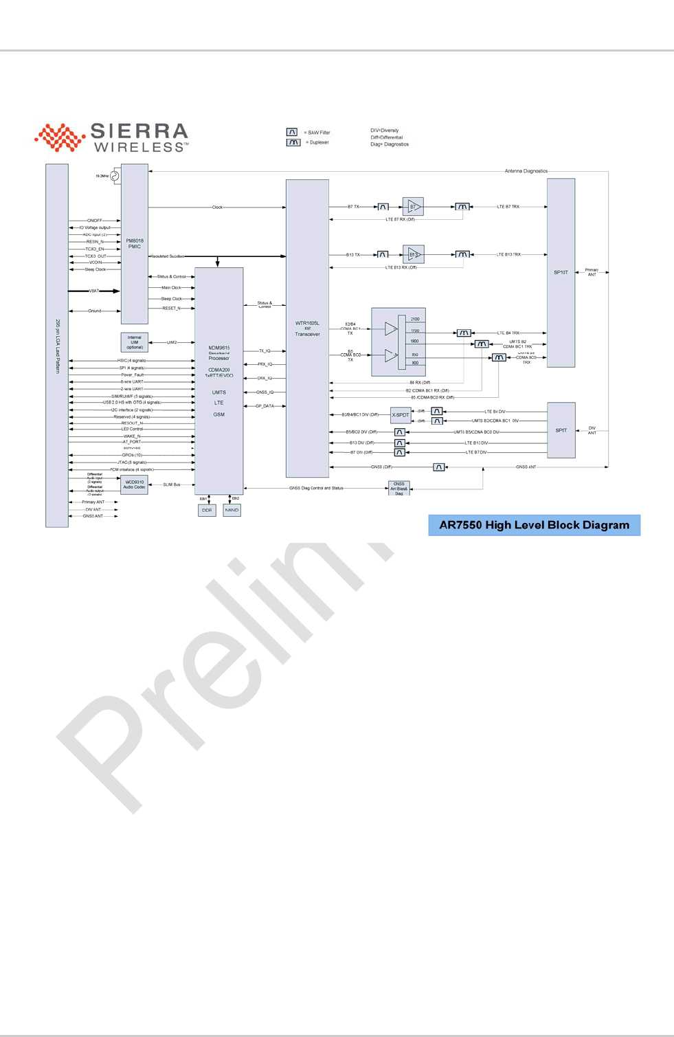
2.3. Block Diagrams
Figure 1. AirPrime AR7550 Block Diagram
4112476 Rev 0.4 March 20, 2013 14
3. Hardware Specifications
3.1. Environmental Specifications
The environmental specification for both operating and storage of the AirPrime AR7550 embedded
modules are defined in the table below.
Table 4. AirPrime AR7550 Environmental Specifications
Parameter Temperature Range Operating Class
Ambient Operating Temperature
-30°C to +75°C Class A
-40°C to -30°C
+75°C to +85°C Class B
Ambient Storage Temperature -40°C to +90°C ---
Ambient Humidity 95% or less ---
Class A is defined as the operating temperature range that the device:
Shall exhibit normal function during and after environmental exposure.
Shall meet the minimum requirements of 3GPP, 3GPP2 or appropriate wireless standards.
Class B is defined as the operating temperature range that the device:
Shall remain fully functional during and after environmental exposure
Shall exhibit the ability to establish a voice, SMS or DATA call (emergency call) at all times
even when one or more environmental constraint exceeds the specified tolerance.
Unless otherwise stated, full performance should return to normal after the excessive
constraint(s) have been removed.
3.2. Electrical Specifications
This section provides details for some of the key electrical specifications of the AirPrime AR7550
embedded modules.
3.2.1. Absolute Maximum and ESD Ratings
This section defines the Absolute Maximum and Electrostatic Discharge (ESD) Ratings of the
AirPrime AR7550 embedded modules.
Warning: If these parameters are exceeded, even momentarily, damage may occur to the device.
Table 5. AirPrime AR7550 Absolute Maximum Ratings
Parameter Min Max Units
VBATT Power Supply Input - 5.0 V
VIN Voltage on any digital input or output pin - VCC_1v8+0.5 V
IIN Latch-up current -100 100 mA
41124764188 Rev 0.41 March 20, 2013 15
Product Technical Specification
Parameter Min Max Units
Maximum Voltage applied to antenna interface pins
VANT
Primary Antenna - 36 V
RX2 Antenna - 36 V
GNSS Antenna - 36 V
ESD Ratings
ESD1 Primary, RX2 and GNSS antenna pads - Contact - ± 8 kV
All other signal pads - Contact - ± 1.5 kV
1 The ESD Simulator configured with 330pF, 1000.
Caution: The AirPrime AR7550 embedded modules are sensitive to Electrostatic Discharge. ESD
countermeasures and handling methods must be used when handling the AirPrime AR7550
devices.
3.3. Mechanical Specifications
3.3.1. Physical Dimensions and Connection Interface
The AirPrime AR7550 embedded modules are a Land Grid Array (LGA) form factor device. The
device does not have a System or RF connectors. All electrical and mechanical connections are made
via the 303 pad LGA on the underside of the PCB.
Table 6. AirPrime AR7550 Embedded Module Dimensions
Parameter Nominal Max Units
Overall Dimension 32 x 37 32.25 x 37.25 mm
Overall Module Height 3.64 3.89 mm
PCB Thickness 1.6 1.76 mm
Flatness Specification - 0.1 mm
Weight tbd - g
Note: The dimensions in Error! Reference source not found. are accurate as of the release date of this
document.
41124764188 Rev 0.41 March 20, 2013 16
Product Technical Specification
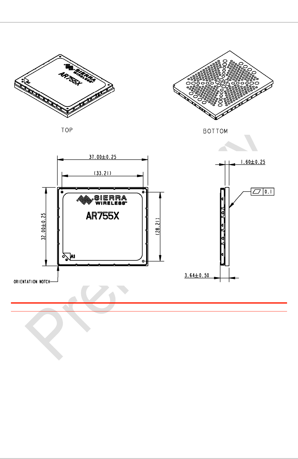
3.3.2. Mechanical Drawing
Figure 2. AR55x Assembly Drawing
Figure 3. AirPrime AR7550 Mechanical Dimensions Drawing
Note: The dimensions in Error! Reference source not found. are preliminary and subject to change.
41124764188 Rev 0.41 March 20, 2013 17
Product Technical Specification
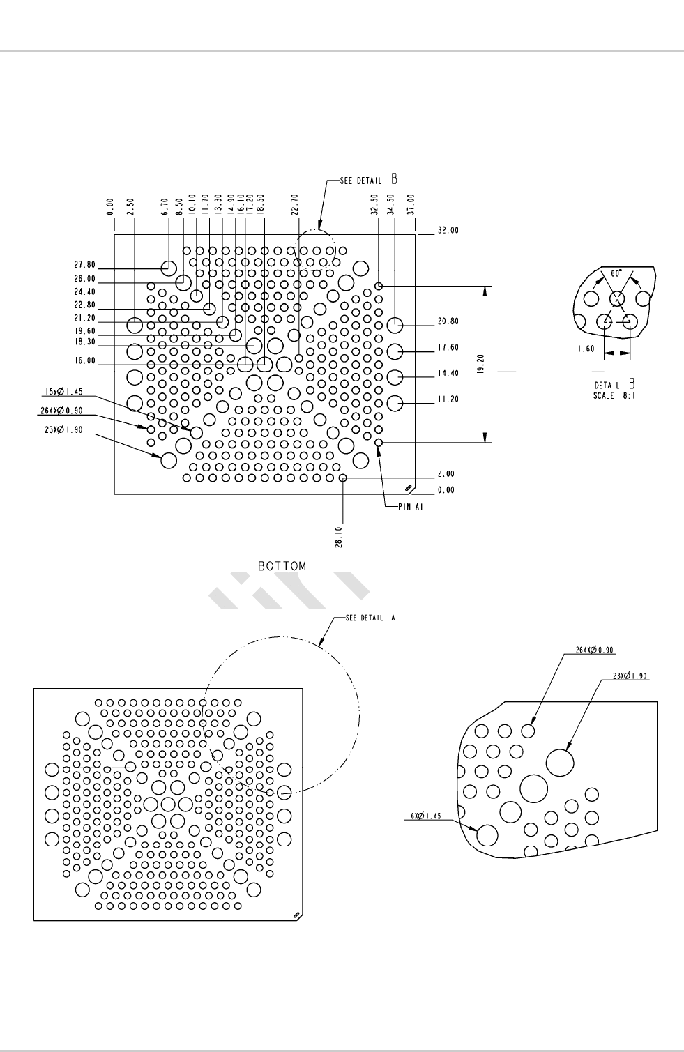
3.3.3. Footprint
The AirPrime AR7550 device LGA footprint is a 303 pad array of 0.9mm, 1.45mm, and 1.90mm pads.
The following drawing illustrates the device footprint. The application footprint is recommended to
mirror the device footprint as illustrated in the following drawing (subject to change).
Figure 4. AirPrime AR7550 Footprint
Figure 5. AirPrime AR7550 Recommended Application Land Pattern
41124764188 Rev 0.41 March 20, 2013 18
Product Technical Specification
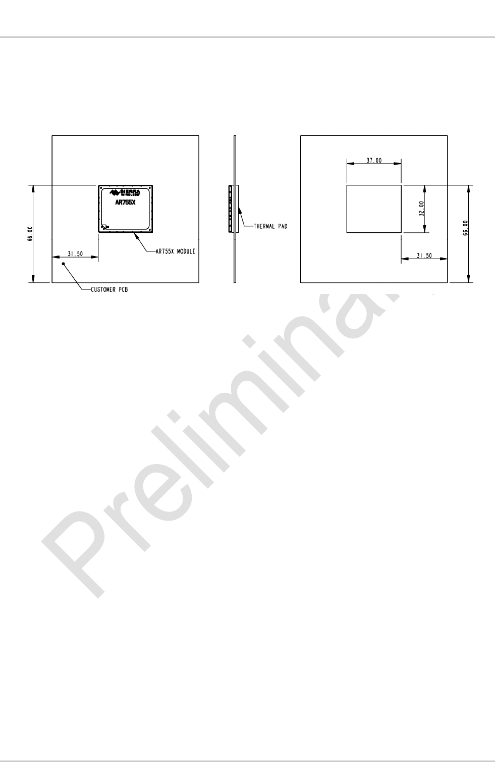
3.3.4. Thermal Consideration
The AirPrime AR7550 device is designed to work over an extended temperature range. In order to do
this efficiently a method of sinking heat from the product is recommended.
Refer to application notes (TBD) for details.
Figure 6. AirPrime AR7550 Heatsink Contact Area
4112476 Rev 0.4 March 20, 2013 19
4. RF Specification
This section presents the WWAN RF interface of the AirPrime AR7550 series of embedded modules.
The specifications for the LTE, CDMA and WCDMA interfaces are defined.
4.1. LTE RF Interface
This section presents the LTE RF Specification for the AirPrime AR7550.
4.1.1. LTE Max TX Output Power
The Maximum Transmitter Output Power of the AirPrime AR7550 embedded modules are specified in
the following table.
Table 7. AirPrime AR7550 Maximum LTE Transmitter Output Power
Band Frequency Band
Nomi
nal
Max
TX
Outp
ut
Powe
r
Tolera
nce
Band 4
+23
dB
+1/‐2
dB
41124764188 Rev 0.41 March 20, 2013 20
Product Technical Specification
Band Frequency Band
Nomi
nal
Max
TX
Outp
ut
Powe
r
Tolera
nce
Band 13 776 MHz to 787 MHz
4.1.2. LTE RX Sensitivity
The Minimum Receiver Sensitivity of the AirPrime AR7550 embedded modules are specified in the
following table.
Table 8. AirPrime AR7550 Minimum LTE Receiver Sensitivity
Band Frequency Band Minimum RX Downlink Criteria
Band 4 1710 MHz to 1755 MHz tbd tbd
Band 7 2500 MHz to 2570 MHz tbd tbd
Band 13 746 MHz to 757 MHz tbd tbd
4.2. CDMA RF Interface
This section presents the CDMA RF Specification for the AirPrime AR7550 embedded modules.
AirPrime AR7550 devices are designed to be compliant with 3GPP2 C.S0011 Rev A and 3GPP2
C.S0033 Rev A v1.0. Parameters specified differently for the reference standard are identified below.
4.2.1. CDMA Max TX Output Power
The Maximum Transmitter Output Power of the AirPrime AR7550 embedded module is specified in
the following table.
41124764188 Rev 0.41 March 20, 2013 21
Product Technical Specification
Table 9. AirPrime AR7550 Maximum CDMA Transmitter Output Power
Band Class Frequency Band Nominal Max TX Output Power Tolerance
BC0 800 MHz +24 dBm +1.5/-1 dB (Class A)
+1.5/-2 dB (Class B)
BC1 1900 MHz
4.2.2. CDMA RX Sensitivity
The Minimum Receiver Sensitivity of the AirPrime AR7550 embedded module is specified in the
following table.
Table 10. AirPrime AR7550 Minimum CDMA Receiver Sensitivity
Band Class Frequency Band Minimum RX downlink Criteria
BC0 800 MHz -106 dBm (Class A)
-104 dBm (Class B) Less than 0.5% FER
BC1 1900 MHz
4.3. WCDMA RF Interface
This section presents the WCDMA RF Specification for the AirPrime AirPrime AR7550 embedded
modules.
4.3.1. WCDMA Max TX Output Power
The Maximum Transmitter Output Power of the AirPrime AR7550 embedded module are specified in
the following table.
Table 11. AirPrime AR7550 Maximum WCDMA Transmitter Output Power
Band Frequency Band Nominal Max TX Output
Power Tolerance
II (1900/PCS) 1850 MHz to 1910 MHz +23.5 dBm +1.5/-1 dB (Class A)
+1.5/-2 dB (Class B)
V (850/CELL) 824 MHz to 849 MHz
4.3.2. WCDMA RX Sensitivity
The Minimum Receiver Sensitivity of the AirPrime AR7550A embedded module are specified in the
following table.
Table 12. AirPrime AR7550 Minimum WCDMA Receiver Sensitivity
Band Frequency Band Minimum RX Downlink Criteria
II (1900/PCS) 1930 MHz to 1990 MHz
-106 dBm (Class A)
-105 dBm (Class B) BER < 0.001
V (850/CELL) 869 MHz to 894 MHz
-107 dBm (Class A)
-106 dBm (Class B)
41124764188 Rev 0.41 March 20, 2013 22
Product Technical Specification
4.4. WWAN Antenna Interface
The specification for the WWAN Antenna Interface of the AirPrime AR7550 embedded modules are
defined in the table below.
Table 13. AirPrime AR7550 WWAN Antenna Characteristics
Characteristics CDMA BC0,
WCDMA B5 CDMA BC1,
WCDMA B2 LTE B4 LTE B13
Frequency (MHz) TX 824-849 1850-1910 1710 – 1755 777 – 787
RX 869-894 1930-1990 2110 – 2155 746 – 756
Impedance RF 50
VSWR max RX 2:1
TX 2:1
Maximum Voltage Primary Antenna – 36 Volts
RX2 Antenna – 36 Volts (LTE MIMO: tbd)
Note: RX2 Antenna port is RX only, RX parameters in the above tables are also applicable.
Table 14. WWAN Antenna Interface Pads
Pad Name Direction Function
BA11 GND Primary Antenna Ground
BA12 PRIMARY_ANT Input/Output Primary Antenna Interface
BA13 GND Primary Antenna Ground
BA7 GND Diversity Antenna Ground
BA8 DIVERSITY_ANT Input Diversity Antenna Interface
BA9 GND Diversity Antenna Ground
4.4.1. WWAN Antenna Recommendations
The table below defines the key characteristics to consider for antenna selection.
Table 15. AirPrime AR7550 WWAN Antenna Recommendations
Characteristics CDMA BC0,
WCDMA B5 CDMA BC1,
WCDMA B2 LTE B4 LTE B13
Frequency (MHz) TX 824-849 1850-1910 1710 – 1755 777 – 787
RX 869-894 1930-1990 2110 – 2155 746 – 756
Impedance RF 50
DC 10 k ±1k
VSWR max RX 1.5: 1
TX 1.5: 1
Polarization Linear, vertical
Typical radiated gain 0 dBi in one direction at least
41124764188 Rev 0.41 March 20, 2013 23
Product Technical Specification
4.5. Primary Antenna Diagnostics
The primary antenna diagnostic feature allows the AirPrime AR7550 embedded module to determine
if the primary antenna connected to the module is: open, shorted or normal. The antenna connected
to this interface needs to have a DC resistance to ground of 10 k ± 1k embedded inside.
The ARx55x FW accepts two limits which are used to evaluate the status of the antenna, representing
the short and open thresholds. Refer to [7] for the syntax of AT+ANTLIMT.
Table 16. Primary Antenna ADC Characteristics
Min Nom Max Units
ADC Voltage Range 0 0.9 1.8 Volts
Resolution - 15 Bit
ADC Values 0 16383
Voltage/ADC step ~0.0011 Volts
1 Assumes 10k Nominal DC resistance in the attached antenna and internal to AirPrime AR7550 device
The following example illustrates the Antenna states and resistance values for a typical limit setting.
AT+ANTLIMT=1,839,1088
Table 17. Primary Antenna Diagnostics Ranges
Antenna State Min ADC Max ADC Antenna Resistance Range
Short 0 839 ~ 7 k
Normal 841 1086 7 k < x < 13 k
Open 1088 1900 13 k
Note: Highlighted numbers in the table above are programmed as shortLim and openLim using the
+ANTLIMT command.
4.6. RX2 Antenna Diagnostics
The RX2 antenna diagnostic feature allows the AirPrime AR75500 to determine if the RX2 antenna
connected to the module is: open, shorted or normal. The antenna connected to this interface needs
to have a DC resistance to ground of 10 k ± 1k embedded inside.
The AirPrime AR7550 FW accepts two limits which are used to evaluate the status of the antenna,
representing the short and open thresholds. Refer to [7] for the syntax of AT+ANTLIMT.
Table 18. RX2 Antenna ADC Characteristics
Min Nom Max Units
ADC Voltage Range 0 0.9 1.8 Volts
Resolution - 15 Bit
ADC Values 0 16383
Voltage/ADC step ~0.0011 Volts
1 Assumes 10k Nominal DC resistance in the attached antenna and internal to AirPrime AR7550 device

41124764188 Rev 0.41 March 20, 2013 24
Product Technical Specification
The following example illustrates the Antenna states and resistance values for a typical limit setting.
AT+ANTLIMT=2,839,1088
Table 19. RX2 Antenna Diagnostics Ranges
Antenna State Min ADC Max ADC Antenna Resistance Range
Short 0 839 ~ 7 k
Normal 841 1086 7 k < x < 13 k
Open 1088 1900 13 k
Note: Highlighted numbers in the table above are programmed as shortLim and openLim using the
+ANTLIMT command.
4112476 Rev 0.4 March 20, 2013 25
5. GNSS Specification
The AirPrime AR7550 embedded module includes optional Global Navigation Satellite System
(GNSS) capabilities via the Qualcomm gpsOne Gen8 Engine, capable of operation in assisted and
stand-alone GPS modes as well as GPS+GLONASS mode.
5.1. GNSS
The GNSS implementation supports GPS L1 operation and GLONASS L1 FDMA operation.
Table 20. GNSS Characteristics
Parameter Value
Sensitivity
Standalone or MS Based Tracking Sensitivity tbd
Cold Start Sensitivity tbd
MS Assisted Synchronous A-GNSS Acquisition Sensitivity tbd
Accuracy in Open Sky (1 Hz tracking) <2m CEP-50
Total number of SV available ~30 SVs
Support for Predicted Orbits Yes
Predicted Orbit CEP-50 Accuracy 5 m
Standalone Time To First Fix (TTFF)
Super Hot 1 s
Warm 29 s
Cold 32 s
Number of channels tbd
GNSS Message Protocols NMEA
Note: Acquisition/Tracking Sensitivity performance figures assume open sky w/ active patch GNSS
antenna and a 2.5 dB Noise Figure.
5.2. GNSS Antenna Interface
The specification for GNSS Antenna Interface is defined in the table below. The AirPrime AR7550
provides biasing for an active antenna as well as onboard circuitry for diagnostics of this antenna
interface.
Table 21. GNSS Antenna Interface Characteristics
Characteristics GNSS
Frequency GPS L1 (Wideband) 1575.42 ± 20 MHz
Glonass L1 FDMA 1597.5 – 1605.8 MHz
RF Impedance 50
VSWR max RX 2:1
LNA Bias Voltage 4.4 – 4.9V, 5.25V (No Load)
LNA Current Consumption 50 mA Max
Maximum Voltage applied to antenna 36 Volts
41124764188 Rev 0.41 March 20, 2013 26
Product Technical Specification
Minimum isolation between the GNSS and WWAN Antenna must be 10 dB for the AirPrime AR7550.
Table 22. GNSS Antenna Interface Pads
Pad Name Direction Function
BA4 GND GNSS Antenna Ground
BA5 GNSS_ANT Input GNSS Antenna Interface
BA6 GND GNSS Antenna Ground
5.2.1. GNSS Antenna Recommendations
The table below defines the key characteristics to consider for antenna selection.
Table 23. GNSS Recommended Antenna Characteristics
Characteristics GNSS
Frequency GPS L1 (Wideband) 1575.42 ± 20 MHz
Glonass L1 FDMA 1597.5 – 1605.8 MHz
RF Impedance 50
VSWR max RX 1.5: 1
LNA Bias Voltage 4.4 – 4.9V
LNA Noise Figure 2.0 dB Max
LNA Current Consumption 50 mA Max
Antenna System Gain (Antenna + LNA - Cable) 20 – 24 dB
Polarization Right Hand Circular Polarization
5.3. GNSS Antenna Diagnostics
The GNSS Antenna Diagnostic feature measures the current drawn by an active GNSS antenna to
determine the state of this antenna interface. Based on the current draw an assessment of open,
short, normal or over-current is made. If an over-current is detected, the bias for the active antenna is
removed to eliminate the fault for drawing excess current which could potentially damage the antenna.
The limits between open/normal and normal/short can be set by the application through an AT
Command.
ADC Value <
openLim < >
shortLim >
GNSS Antenna State Open Normal Short
The Over Current limit is set by hardware and cannot be altered.
Table 24. GNSS Antenna Diagnostics Ranges
Control State Min Max Units
HW Over Current 78 100 mA
The GNSS antenna supply is powered from VBATT through a boost regulator.
41124764188 Rev 0.41 March 20, 2013 27
Product Technical Specification
The following table identifies some key VGNSS_ANT current draw values and the associated ADC
values.
Table 25. VGNSS_ANT Current Draw
I (mA) Nominal
0 337
5 612
10 936
15 1242
20 1558
25 1877
30 2194
35 2494
40 2821
45 3188
50 3444
55 3747
60 4065
65 4292
70 4319
The graph below illustrates the relationship between current drawn on VGNSS_ANT vs the ADC
readings used to monitor the GNSS Antenna status.
41124764188 Rev 0.41 March 20, 2013 28
Product Technical Specification
Figure 7. VGNSS_ANT vs. ADC Readings Relationship
PM8018
150K
BOOSTREG
VIN VOUT
FB
BOOST_CTRL
200V/V
Converter
S+ S‐
Vout
PMIC
MPP_02
MDM9X15
GPIO_09
GPIO_69
LGA
VBATT 330m
ILim
VIN VOUT
FLAGB
ON
GPIO_59
10K
GNSSPWR_EN
ILIM_EN
ILIM_OC_N
VGNSS
5V
CurrentLimit=75mA
0~4.35V
GNSS_ANT_ADC
5V
Figure 8. GNSS Power Supply and Antenna Diagnostics Block Diagram
41124764188 Rev 0.41 March 20, 2013 29
Product Technical Specification
5.4. Current Consumption
The table below summarizes some key current consumption values for various modes of the AirPrime
AR7550 devices.
Table 26. AirPrime AR7550 Current Consumption Values
Mode Parameter Typical Max Units
On Call – CDMA
Maximum TX Output – 1xRTT/1xEVDO - tbd mA
+0dBm TX Output – 1xRTT tbd - mA
+0dBm TX Output – 1xEVDO tbd - mA
On Call – WCDMA
Maximum TX Output – WCDMA/HSPA - tbd mA
+0dBm TX Output – WCDMA tbd - mA
+0dBm TX Output – HSPA tbd - mA
On Call – LTE Maximum TX Output - tbd mA
+0dBm TX Output tbd - mA
Idle – CDMA Registered USB Enumerated tbd - mA
USB Not Enumerated tbd - mA
Searching for network – CDMA tbd - mA
Idle – WCDMA Registered USB Enumerated tbd - mA
USB Not Enumerated tbd - mA
Searching for network – WCDMA tbd - mA
Idle – LTE Registered USB Enumerated tbd - mA
USB Not Enumerated tbd - mA
Searching for network – LTE tbd - mA
Sleep Mode
Average current, QPCH, SCI=2 - tbd mA
Average current, WCDMA, DRX=8 - tbd mA
Average current, LTE - tbd mA
Off Power OFF Current tbd tbd A
GNSS
Acquisition (Airplane mode, cold start) tbd mA
Tracking (Registered) tbd mA
Powering an Active Antenna from VGNSS_ANT tbd mA
1 This is the additional current draw on VBATT for 10mA consumption by Active LNA from VGNSS_ANT. Higher current
consumption by the antenna will result in higher consumption on VBATT.
5.5. Digital IO Characteristics
The Digital IO characteristics are defined in the table below. These apply to GPIOs, UART, LED,
SDIO and PCM/I2S.
Table 27. Digital IO Characteristics
Parameter Comments Min Typ Max Units
VIH High level input
voltage CMOS/Schmitt 0.65* VCC_1V8 – VCC_1V8+0.3 V
41124764188 Rev 0.41 March 20, 2013 30
Product Technical Specification
Parameter Comments Min Typ Max Units
VIL Low level input
voltage CMOS/Schmitt -0.3 – 0.35* VCC_1V8 V
VOH High level
output voltage
CMOS, at pin rated drive
strength VCC_1V8 - 0.45 – VCC_1V8 V
VOL Low-level output
voltage
CMOS, at pin rated drive
strength 0 – 0.45 V
IOH High level
output current
VOH = VCC_1V8 – 0.45
V – – 6 mA
IOL Low Level
output current VOL = 0.45 V -6 – – mA
IOH-LED High level
output current LED signal only – – – mA
IOL-LED Low Level
output current LED signal only -3 – 20 mA
IIHPD Input high
leakage current With pull-down 5 30 µA
IILPU Input low
leakage current With pull-up -30 -5 µA
IL Input leakage
current
VIO = max,
VIN = 0 V to VIO
LED signal only
-0.3 – +0.35 µA
CIN Input
capacitance – – 7 pF
CIN-LED Input
capacitance LED signal only – – 5 pF
Caution: Digital IOs shall not be pulled-up to an external voltage as this may cause VCC_1V8 to not go low
when the AirPrime AR7550 device is powered down. Also, this would partially bias the AirPrime
AR7550 device which could potentially damage the device or result in GPIOs being set to
undetermined levels.
5.6. Internal Device Frequencies
The table below summarizes the frequencies generated within the AirPrime AR7550. This table is
provided for reference only to the device integrator.
Table 28. Internal Device Frequencies
Subsystem/Feature Frequency Units
Real Time Clock 32.768 kHz
PCM Audio interface (Primary PCM Master Mode) [TBD]
8,
128,
2048
kHz
I2C Interface 400 kHz
PMIC switching power supplies tbd MHz
GNSS Antenna bias switching supply 3.5 MHz

41124764188 Rev 0.41 March 20, 2013 31
Product Technical Specification
Subsystem/Feature Frequency Units
Fundamental clock, codec, TCXO_OUT 19.2 MHz
PLL tbd MHz
USB 12,
480 Mb/s
4112476 Rev 0.4 March 20, 2013 32
6. Baseband Specification
6.1. Power Supply
The AirPrime AR7550 embedded module is powered via a single regulated DC power supply, 3.7V
nominal. The power supply requirements can be found in the following table.
Table 29. Power Supply Requirements
Power Supply Min Typ Max Units
Main DC Power Input Range 3.4 3.7 4.2 V
Power Supply Ripple 0 to 1kHz - - 200 mVpp
>1kHz - - 50 mVpp
Maximum Current draw AR7550 - - tbd mA
AirPrime AR7550 does not support USB bus-powered operation. DC power must be supplied via the
VBATT input.
Table 30. Power Supply Pads
Pad Name Direction Function If Unused
EA2 VBATT Input Power Supply Input Must Be Used
EB2 VBATT Input Power Supply Input Must Be Used
EC2 VBATT Input Power Supply Input Must Be Used
6.1.1. Under-Voltage Lockout (UVLO)
The power management section of the AirPrime AR7550 includes an under-voltage lockout circuit that
monitors supply and shuts down when VBATT falls below the threshold.
Figure 9. Under-Voltage Lockout (UVLO) Diagram
The AirPrime AR7550 will power down and remain off until the level of VBATT returns to the valid
range and the ON/OFF signal is active.
41124764188 Rev 0.41 March 20, 2013 33
Product Technical Specification
Note: If the AirPrime AR7550 device has 6 UVLO events without a valid power down or reset sequence, it
enters a mode in which only the DM port enumerates on the USB.
Table 31. UVLO Thresholds
Description Value Units
UVLO
Rising threshold 2.725 V
Falling threshold 2.55 V
Minimum Duration below Falling threshold 1.0 uS
6.2. VCOIN
The AirPrime AR7550 provides an interface for a coin cell to maintain the internal RTC when VBATT
is removed from the AirPrime AR7550 device. Whenever VBATT is applied the RTC is powered from
the VBATT supply. The AirPrime AR7550 also supports charging of a coin cell if connected to this
interface.
Table 32. VCOIN Pad
Pad Name Direction Function If Unused
AC11 VCOIN Input /Output Voltage Input/Charging output Leave Open
The table below defines the specifications of this interface.
Table 33. VCOIN Interface Specification
VCOIN Min Typ Max Units
DC Power Input Range TBD TBD TBD V
Current Draw 1.1 2.0 A
The table below defines the VCOIN charging specifications.
Table 34. VCOIN Charging Specifications
VCOIN Charging Specs Comments Min Typ Max Units
Target regulator voltage1 VIN > 2.5 V, ICHG = 100 A TBD TBD TBD V
Target series resistance2 800 – 2100
Coin cell charger voltage error ICHG = 0 A -5 – +5 %
Coin cell charger resistor error -20 – +20 %
Dropout voltage3 ICHG = 2 mA – – 200 mV
Ground current, charger enabled
VBAT = 3.6 V, T = 27 ºC
VBAT = 3.2 to 4.2 V
IC = off; VCOIN = open
–
–
4.5
–
–
8
A
A
1. Valid regulator voltage settings are 2.5, 3.0, 3.1, and 3.2 V.
2. Valid series resistor settings are 800, 1200, 1700, and 2100 .
3. Set the input voltage (VBAT) to 3.5 V. Note the charger output voltage; call this value V0. Decrease the input voltage
until the regulated output voltage drops 100 mV (until the charger output voltage = V0 - 0.1 V). The voltage drop across
the regulator under this condition is the dropout voltage (Vdropout = VBAT - the charger output voltage).
41124764188 Rev 0.41 March 20, 2013 34
Product Technical Specification
6.3. ON/OFF Control
The AirPrime AR7550 provides an interface for controlling the device ON/OFF state.
Table 35. ON/OFF Control Pads
Pad Name Direction Function If Unused
BB1 ON/OFF Input ON/OFF Control Must Be Used
The ON/OFF signal is internally pulled up to an internal 1.8V reference voltage. An open drain
transistor should be connected to this pin to generate a low pulse. This pin should not be driven high
external to the AirPrime AR7550 embedded module.
Table 36. ON/OFF Internal Pull-Up
Signal Parameter Min Typ Max Units
ON/OFF Internal Pull-up - 200 - k
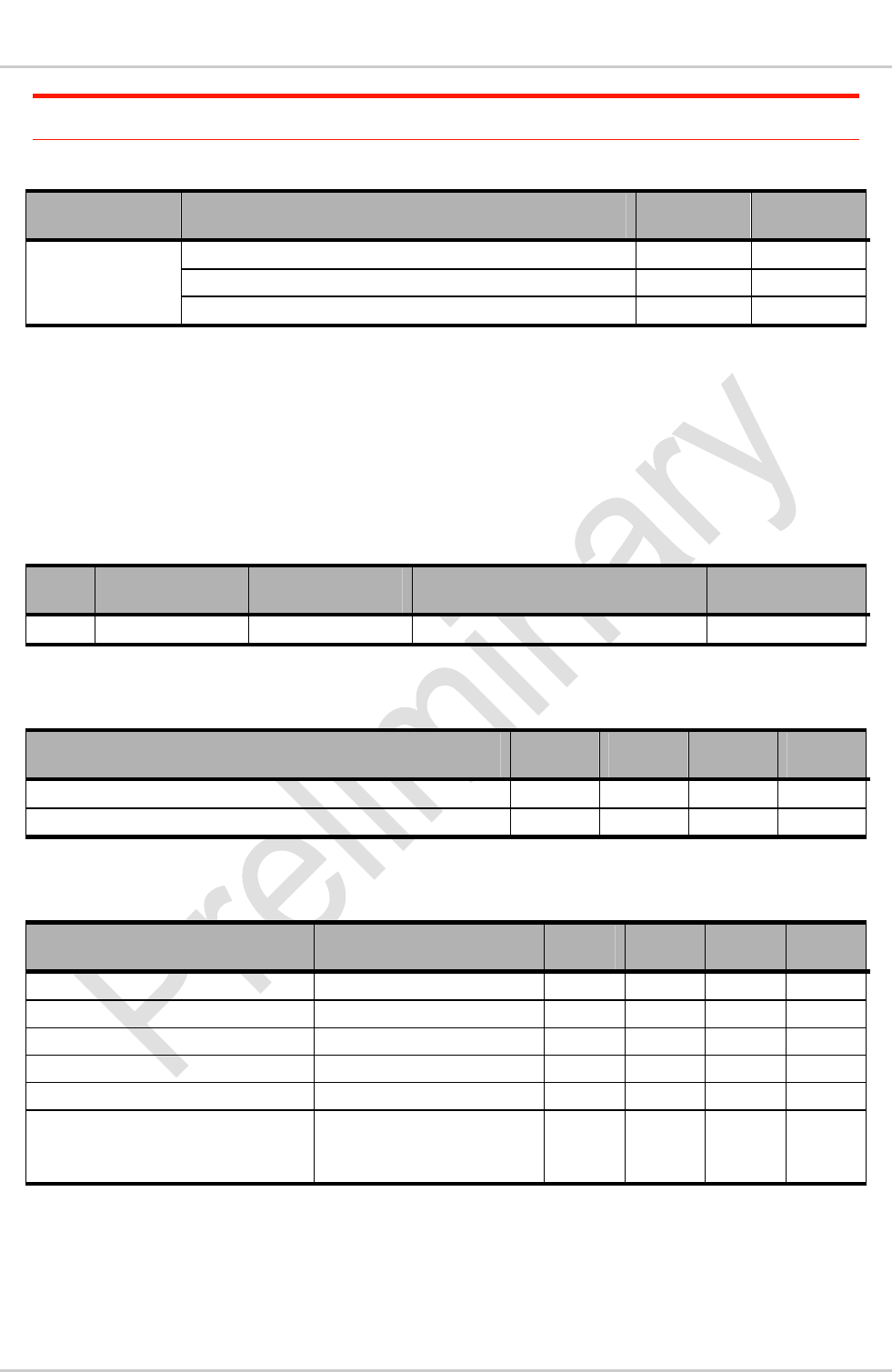
6.3.1. ON/OFF Timing
The ON/OFF pin is a low pulse toggle control. The first pulse powers the AirPrime AR7550 ON, a
second pulse instructs the AirPrime AR7550 to begin the Shutdown process.
The diagram below illustrates the recommended application implementation for ON/OFF control.
Figure 10. Recommended ON/OFF Control
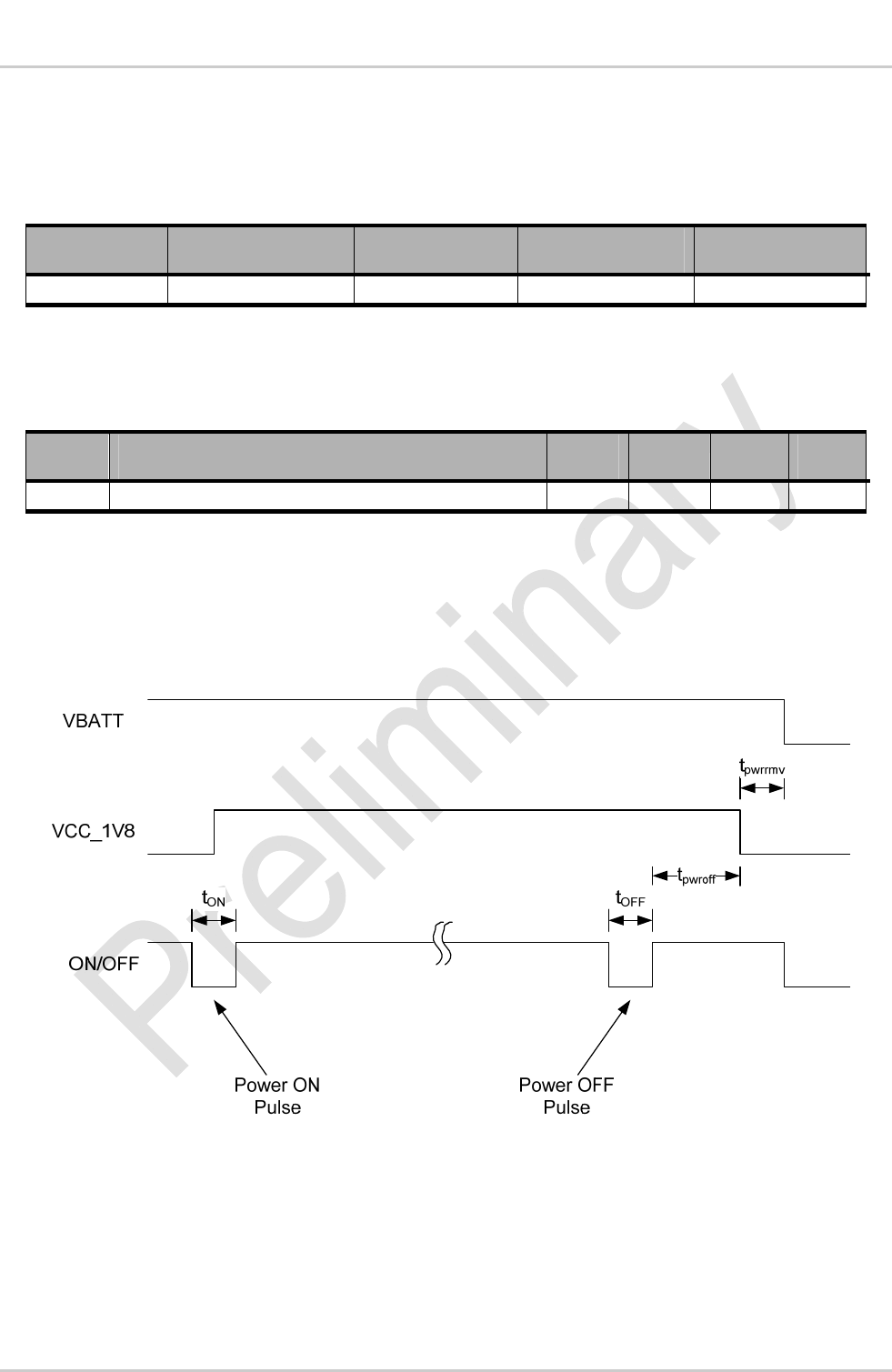
The diagram below illustrates an alternate application implementation that holds ON/OFF low during
operation.
41124764188 Rev 0.41 March 20, 2013 35
Product Technical Specification
Figure 11. Alternate ON/OFF Control
Table 37. Power-ON Sequence Symbol Definitions
Symbol Parameter Boot Min Typ Max
tON Turn ON Pulse duration 50 ms 100 ms
tOFF Turn OFF Pulse duration 50 ms 100 ms 500 ms
tpwroff Time to Power OFF - 5 s -
tpwrrmv Time VBATT must be maintained after VCC_1V8
goes inactive 0 s - -
tHI Time required for ON/OFF to be high prior to OFF
pulse.
In process 10 s -
Complete 50 ms
Tpwroff is the time between when a power OFF pulse is complete and when shutdown is completed by
the AirPrime AR7550 devices. This duration is network and device dependent, i.e. in a CDMA network
a power down registration is initiated by the AirPrime AR7550 device, when the acknowledgement is
received from the network power OFF completes.
Detection of power down can be accomplished by monitoring for one of the following:
+WIND: 10 output on the AT Command interface
USB ports are de-enumerated
The application must wait for a power down to be detected prior to removing power from the AirPrime
AR7550 device. If a timeout is required, it is recommended to be in excess of 30s prior to removing
power from the AirPrime AR7550 device.
Note: Refer to [7] for details on enabling the +WIND message for power down and +USLGRPMSK and
+USLEVTMSK for unsolicited message output.
41124764188 Rev 0.41 March 20, 2013 36
Product Technical Specification
6.3.3. Software-Initiated Power Down
The host application may choose to use the AT Command AT!POWERDOWN to initiate a power
down of the AirPrime AR7550 device instead of using an OFF pulse. In this scenario the ON/OFF
signal should be left open by the application. The AirPrime AR7550 device will initiate a power up
after completion of the power down if ON/OFF is low.
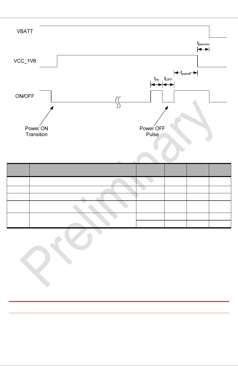
6.3.4. Deep Sleep
The AirPrime AR7550 embedded modules support a low power mode in which the device is
registered on the LTE/CDMA/GSM/WCDMA network and sleeps in between wake intervals where it
listens for pages.
Figure 12. Power Mode Diagram
The following table lists the parameter that defines the wake interval period for the various devices.
Table 38. Period of Wake Intervals
AR Series Device Network Standard Parameter
AR7550
CDMA SCI
WCDMA DRX
LTE DRX
The average current consumption of the AirPrime AR7550 while in this mode is defined in the Sleep
Mode portion of the current consumption tables in section 5.4 Current Consumption.
The Slot Cycle Index is the lower of the values stored in the AirPrime AR7550 or the value being
broadcast by the wireless network that the AirPrime AR7550 is registered on.
The MFRM and DRX cycle index values are broadcast by the wireless network on which the AirPrime
AR7550 embedded module is registered.
While in Deep Sleep mode the functions of the AirPrime AR7550 are limited as defined in the
following table.
Table 39. Deep Sleep Function Availability
Function Availability Conditions
Paging
41124764188 Rev 0.41 March 20, 2013 37
Product Technical Specification
Function Availability Conditions
GNSS - GNSS is powered down
Time measurement
USB - USB_VBUS is not applied
UART -
Digital IO - Digital IO pins maintained last state
Events that cause the AirPrime AR7550 to wake-up from Deep Sleep mode include:
Incoming call
Expiration of an internal timer in the AirPrime AR7550
USB_VBUS is applied to the AirPrime AR7550
WAKE_N is asserted (low)
UART1 DTR is asserted (high) if UART1 DTR has been enabled as a sleep control
(AT+W32K=1,1) and AT Command Service is mapped to UART1
GNSS location fix request is initiated from an Embedded Application
See the Ring Indicator section for more information about configuring the RI signal to notify an
external application of a wake-up event while the AR device is in sleep mode.
6.3.4.1. Sequence to Enter Deep Sleep Mode
The following list defines the sequence needed by the application to allow the AirPrime AR7550 to
enter Deep Sleep mode:
1. AR7550 has registered on the WWAN network (or callbox), and is not in a call.
2. End GNSS Tracking session.
3. Turn off GNSS Antenna bias.
4. Confirm WAKE_N is not held low (pulled-up in AirPrime AR7550).
5. Issue AT command to request AR device to enter deep sleep (AT+W32K=1,x).
6. If AT+W32K=1,1 is used, DTR must also be de-asserted to allow sleep.
7. Ensure UARTs are in the inactive state.
8. Remove VBUS from being applied to the AR device.
6.4. USB
The AirPrime AR7550 has a High Speed USB2.0 compliant, peripheral only interface.
Table 40. USB Pad Details
Pad Name Direction Function
DA7 USB_VBUS Input USB Power Supply
DB6 USB_D_P In/Out Differential data interface positive
DA6 USB_D_M In/Out Differential data interface negative
DD5 USB_ID In/Out USB ID
The AR7550 will not be damaged if a valid USB_VBUS is supplied while the main DC power is not
supplied.
41124764188 Rev 0.41 March 20, 2013 38
Product Technical Specification
Table 41. USB Characteristics
USB Value Units
USB_VBUS
Voltage range 2.0 – 5.25 V
Maximum Current draw1 1 mA
Maximum Input Capacitance (Min ESR = 50 m) 10 F
1 With the AirPrime AR7550 device powered ON.
6.5. UART
The AirPrime AR7550 has two UART interfaces. The primary UART is an 8-wire1 electrical interface
and the secondary UART is a 2-wire electrical interface.
Table 42. UART Pads
Pad Name Direction Function Interface If Unused
AD9 RXD1 Output Receive Data (UART1) UART1 Leave Open
AE6 RTS1 Input Ready To Send (UART1) UART1 Leave Open1
AD8 TXD1 Input Transmit Data (UART1) UART1 Leave Open
AE7 CTS1 Output Clear To Send (UART1) UART1 Leave Open
AF6 DCD1 Output Data Carrier Detect (UART1) UART1 Leave Open
AE5 DTR1 Input Data Terminal Ready (UART1) UART1 Leave Open
AF5 DSR1 Output Data Set Ready (UART1) UART1 Leave Open
DB2 RXD2 Output UART2 Receive Data UART2 Leave Open
DA2 TXD2 Input UART2 Transmit Data UART2 Leave Open
1 If UART1 is implemented as a 2-wire interface, RTS1 should be pulled low to disable flow control.
6.6. Ring Indicator
The Ring Indicator (RI) may be used to notify an external application of several events such as an
incoming call, timer expiration or incoming SMS.
Table 43. Ring Indicator Pad
Pad Name Direction Function If Unused
AD7 RI1 Output Ring Indicator Leave Open
The events which toggle the RI signal can be configured using the AT+WWAKESET command. The
duration of the RI pulse can be configured using the AT+WRID command.
The reason for the RI signal being activated can be queried using the AT+WWAKE command. Refer
to [7] for details of these AT Commands.
The RI signal is independent of the UART.
1 Includes Ring Indicator which may also be used independently of UART1.
41124764188 Rev 0.41 March 20, 2013 39
Product Technical Specification
6.7. UIM Interface
The UIM interface of the AirPrime AR7550 supports a USIM/CSIM for LTE, WCDMA, GSM and
CDMA. The UIM can be embedded internally in AR7550 and can be external to AR7550.
Table 44. UIM Pads
Pad Name Direction Function If Unused
DA5 UIM_DETECT Input Detection of an external UIM card Leave Open
DB4 UIM_VCC Output Supply output for an external UIM card Leave Open
DC3 UIM_RST Output Reset output to an external UIM card Leave Open
DA4 UIM_DAT Input /Output Data connection with an external UIM card Leave Open
DE1 UIM_CLK Output Clock output to an external UIM card Leave Open
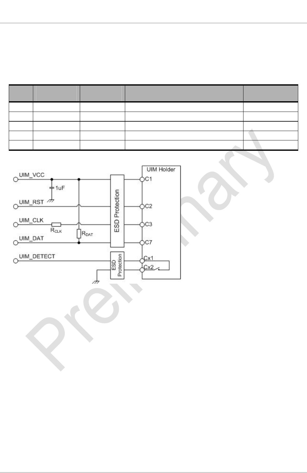
The diagram below illustrates the recommended implementation of a UIM holder on the application.
Figure 13. Recommended UIM Holder Implementation
UIM_DETECT is used to detect the physical presence of a SIM/UIM card in the holder. It has a 3.0uA
to 30µA pull-up to 1.8V inside the AirPrime AR7550. It should be set to GND if a SIM/UIM is present.
All signals must be ESD-protected near the UIM holder.
The capacitor and two resistors should be added as placeholders to compensate for potential layout
issues. UIM_DAT trace should be routed away from the UIM_CLK trace. Keep distance from AirPrime
AR7550 to UIM-Holder as short as possible.
An ESD device specifically designed for SIM/UIM cards is recommended for UIM_VCC, UIM_RST,
UIM_CLK and UIM_DAT. i.e. SEMTECH EClamp2455K, Infineon BGF106C or NXP IP4264CZ8-20-
TTL. For UIM_DETECT a low leakage ESD suppressor should be selected.
6.7.1. Internal UIM
Alternatively, a hardware option is available that includes a UIM device mounted on the AirPrime
AR7550 PCB thus eliminating the need for an external UIM holder
41124764188 Rev 0.41 March 20, 2013 40
Product Technical Specification
6.8. General Purpose IO
The AirPrime AR7550 defines 10 GPIOs for customer use.
Table 45. GPIO Interface Pads
Pad Name Pull State Function If Unused Multiplexed
Function
CA10 GPIO1 Pull-Down Available-GPIO Leave Open
CA11 GPIO2 Pull-Down Available-GPIO Leave Open
CB10 GPIO3 Pull-Down Available-GPIO Leave Open
CB11 GPIO4 Pull-Down Available-GPIO Leave Open
CC7 GPIO5 Pull-Down Available-GPIO Leave Open
CC8 GPIO6 Pull-Down Available-GPIO Leave Open
CC9 GPIO7 Pull-Down Available-GPIO Leave Open
CD7 GPIO8 Pull-Down Available-GPIO Leave Open Band indicator1
CE5 GPIO9 Pull-Down Available-GPIO Leave Open Band indicator2
CF5 GPIO10 Pull-Down Available-GPIO Leave Open Band indicator3
Refer to the Digital IO Characteristics section for electrical characteristics of these signals.
6.8.1. AT Port Switch
The AirPrime AR7550 supports switching the active AT command port between USB and UART.
Table 46. AT Port Switch States
Pad Name State AT Port
AB5 AT_PORT_SW
Low (default) Available on USB
High Available on UART1
6.9. Secure Digital IO
The AirPrime AR7550 defines a 1.8V SDIO interface for future use.
Table 47. SDIO Interface Pads
Pad Name Direction Function If Unused
AA11 SDIO_DATA0 Input/Output SDIO Data bit 0 Leave Open
AA10 SDIO_DATA1 Input/Output SDIO Data bit 1 Leave Open
AB9 SDIO_DATA2 Input/Output SDIO Data bit 2 Leave Open
AB10 SDIO_DATA3 Input/Output SDIO Data bit 3 Leave Open
AB8 SDIO_CMD Output SDIO Command Leave Open
AA9 SDIO_CLK Output SDIO Clock Leave Open
41124764188 Rev 0.41 March 20, 2013 41
Product Technical Specification
6.10. I2C
The AirPrime AR7550 provides an I2C interface.
Table 48. I2C Interface Pads
Pad Name Direction Function If Unused
CD6 I2C_CLK Output I2C Clock output Leave Open
CC6 I2C_SDA Input/Output I2C Data Leave Open
The I2C signals are open drain outputs with 2.2 k pull-up resistors to VCC_1V8 internal to the
AirPrime AR7550.
6.11. Voltage Reference
The AirPrime AR7550 utilizes 1.8V logic. A voltage reference output for this rail is provided below.
Table 49. Voltage Reference Pad
Pad Name Direction Function If Unused
AA12 VCC_1V8 Output Voltage Reference Output Leave Open
AB12 VCC_1V8 Output Voltage Reference Output Leave Open
Table 50. Voltage Reference Characteristics
Parameter Min Typ Max Units
VCC_1V8
Voltage Level 1.746 1.8 1.854 V
Output Current 25 mA
The VCC_1V8 signal can be used to power external circuitry and/or detect the power state of the
AirPrime AR7550 device.
Using VCC_1V8 to determine the power state is recommended when the user application wants to
disable VBATT. VBATT should not be disabled before VCC_1V8 goes inactive. To be able to detect
the power state on VCC_1V8, all logic input signals to the AirPrime AR7550device must be set low
(see Digital IO Characteristics for affected signal groups).
The VCC_1V8 signal is High-Z when the AirPrime AR7550 embedded module is powered down.
6.12. RESET
The AirPrime AR7550 provides an interface to allow an external application to RESET the module as
well as an output to indicate the current RESET state or control an external device.
Table 51. Reset Interface Pads
Pad Name Direction Function If Unused
AH2 RESIN_N Input External Reset Input Leave Open
AG4 RESOUT_N Output Reset Output Leave Open
41124764188 Rev 0.41 March 20, 2013 42
Product Technical Specification
The RESIN_N signal is pulled-up internal to the AirPrime AR7550. An open collector transistor or
equivalent should be used to Ground the signal when necessary to RESET the module.
Note: Use of the RESIN_N signal to RESET the AirPrime AR7550 could result in memory corruption if
used inappropriately. This signal should only be used if the AirPrime AR7550 has become
unresponsive and it is not possible to perform a power cycle.
Table 52. Reset Timing
Symbol Parameter Min Typ Max
Trdet Duration of RESIN_N signal before firmware detects it
(debounce timer) - 32 ms -
Trlen Duration reset asserted 40 ms -
Trdel Delay between minimum Reset duration and Internal Reset
generated - 500 ms -
Figure 14. Illustration of Reset Timing When RESIN_N < Trdel
Figure 15. Illustration of Reset Timing When RESIN_N Held Low > Trdet+Trdel
6.13. ADC
The AirPrime AR7550 provides two ADC inputs. The interface information is provided in the tables
below.
Table 53. ADC Interface Pads
Pad Name Direction Function If Unused
DE3 ADC0 Input Analog to Digital Converter Input Leave Open or Ground
DF2 ADC1 Input Analog to Digital Converter Input Leave Open or Ground
41124764188 Rev 0.41 March 20, 2013 43
Product Technical Specification
Table 54. ADC Interface Characteristics
ADC Value Units
ADCx
Full-Scale Voltage Level 1.8 V
Resolution 15 bit
Input Impedance >4 M
6.14. LED
The AirPrime AR7550 provides an LED control output signal pad. This signal is an open drain input.
Table 55. LED Interface Pad
Pad Name Direction Function If Unused
AA6 LED Output LED driver control Leave Open
Figure 16. LED Reference Circuit
The behavior of the LED signal can be modified using the AT command AT!LEDCTRL.
6.15. Audio
The AirPrime AR7550 supports both Analog and Digital audio interfaces. The following diagram
illustrates the Audio subsystem and identifies where various AT commands affect the audio
subsystem. Refer to [7] for details of the AT commands.
[Diagram tbd]
Figure 17. Audio Block Diagram
6.15.1. Analog Audio
The AirPrime AR7550 provides a mono differential analog audio interface.
Table 56. Analog Audio Interface Pads
Pad Name Direction Function Interface
CD9 AUDIO1_IN_P Input Microphone 1 input positive
Primary
CC10 AUDIO1_IN_M Microphone 1 input negative
CE6 AUDIO1_OUT_P Output Speaker 1 output positive
CE8 AUDIO1_OUT_M Speaker 1 output negative
41124764188 Rev 0.41 March 20, 2013 44
Product Technical Specification
Table 57. Analog Audio Interface Characteristics
Analog Audio Min. Typ. Max. Units
Audio IN
Input Impedance 16 20 24 k
Signal Level – Differential -0.3 - 2.9 dBV
Signal Level – Single-ended
(the unused audio signal must be tied to
GND or analog reference)
-0.3 - 2.9 dBV
Audio OUT
Signal Level – Differential - - dBV
Signal Level – Single-ended -0.3 - 2.9 dBV
Output Impedance -0.3 - 2.9
Signal Drive Strength – Application Load - 600 1M k
6.15.2. Digital Audio
The AirPrime AR7550 provides a 4-wire digital audio interface. This interface can be configured as
either a PCM or an I2S.
Table 58. Digital Audio Interface Pads
Pad Name Direction1 PCM
Function Direction I2S Function If Unused
DB3 PCM_FS Output PCM Frame
Sync Input/Output I2S_WS Leave Open
DA3 PCM_CLK Output PCM Clock Input/Output I2S_SCLK Leave Open
DC2 PCM_DOUT Output PCM Data Out Output I2S_DOUT Leave Open
DD2 PCM_DIN Input PCM Data In Input I2S_DIN Leave Open
1 Direction when defined in Master mode.
6.15.2.1. PCM
The AirPrime AR7550 PCM interface can be configured in one of two modes: primary PCM or
auxiliary PCM mode. The table below defines the configurations for each of these two modes.
Table 59. PCM Interface Configurations
Element Primary PCM Auxiliary PCM
Slot Configuration Slot-based Single
Sync type Short Long
Frequency 8 kHz
Duty Cycle 50%
Clock (Master) 2.048 MHz 128 kHz
Data formats 16-bit linear, 8-bit A-law, 8-bit m-law
AirPrime AR7550 Master/Slave Master or Slave Master
41124764188 Rev 0.41 March 20, 2013 45
Product Technical Specification
6.15.2.1.1. PCM Data format
The PCM data is 8 kHz and 16 bits with the following PDM bit format:
PCM_DIN – SDDD DDDD DDDD DDVV
PCM_DOUT – SDDD DDDD DDDD DDVV
Where:
S – Signed bit
D – Data
V – Volume padding
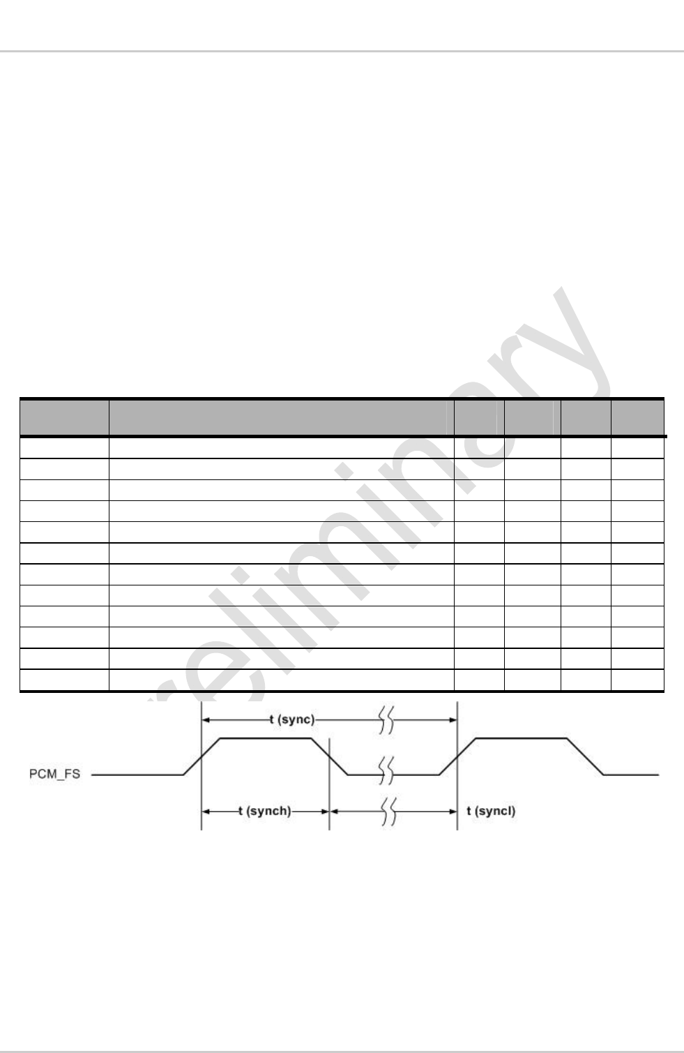
6.15.2.1.2. Primary PCM Timing
The table and drawings below illustrate the PCM signals timing when the AirPrime AR7550 module is
operating in Primary PCM mode.
Table 60. Primary PCM Timing
Parameter Description Min Typ Max unit
T(sync) PCM_FS cycle time - 125 - µs
T(synch) PCM_FS high time - 488 - ns
T(syncl) PCM_FS low time - 124.5 - µs
T(clk) PCM_CLK cycle time - 488 - ns
T(clkh) PCM_CLK high time - 244 - ns
T(clkl) PCM_CLK low time - 244 - ns
T(susync) PCM_FS setup time high before falling edge of PCM_CLK - 122 - ns
T(hsync) PCM_FS Hold time after falling edge of PCM_CLK - - 366 ns
T(sudin) PCM_DIN setup time before falling edge of PCM_CLK 60 - - ns
T(hdin) PCM_DIN hold time after falling edge of PCM_CLK 60 - - ns
T(pdout) Delay from PCM_CLK rising to PCM_DOUT valid - - 60 ns
T(zdout) Delay from PCM_CLK falling to PCM_DOUT HIGH-Z - - 60 ns
Figure 18. PCM_FS Timing Diagram (2048 kHz Clock)
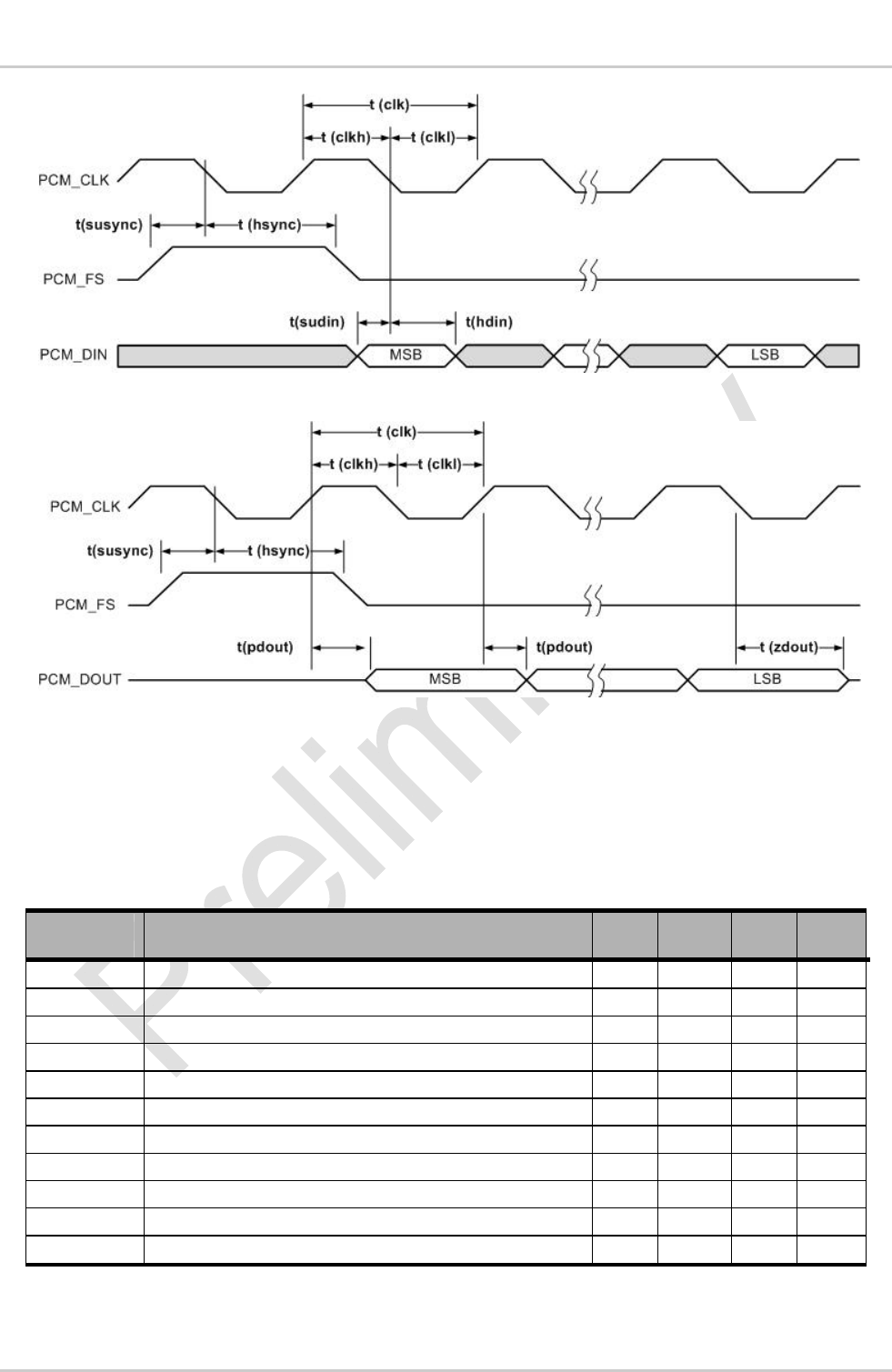
41124764188 Rev 0.41 March 20, 2013 46
Product Technical Specification
Figure 19. PCM Codec to AR Device Timing Diagram (Primary PCM)
Figure 20. AR Device to PCM Codec Timing Diagram (Primary PCM)
6.15.2.1.3. Auxiliary PCM Timing
The table and drawings below illustrate the timing of the PCM signals when the AirPrime AR7550
module is operating in Auxiliary PCM mode.
Table 61. Auxiliary PCM Timing
Parameter Description Min Typ Max unit
T(auxsync) PCM_FS cycle time - 125 - µs
T(auxsynch) PCM_FS high time 62.4 62.5 - µs
T(auxsyncl) PCM_FS low time 62.4 62.5 - µs
T(auxclk) PCM_CLK cycle time - 7.8 - µs
T(auxclkh) PCM_CLK high time 3.8 3.9 - µs
T(auxclkl) PCM_CLK low time 3.8 3.9 - µs
T(suauxsync) PCM_FS setup time high before falling edge of PCM_CLK 1.95 - - ns
T(hauxsync) PCM_FS Hold time after falling edge of PCM_CLK 1.95 - - ns
T(sudin) PCM_DIN setup time before falling edge of PCM_CLK 70 - - ns
T(hauxdin) PCM_DIN hold time after falling edge of PCM_CLK 20 - - ns
T(pauxdout) Delay from PCM_CLK rising to PCM_DOUT valid - - 50 ns
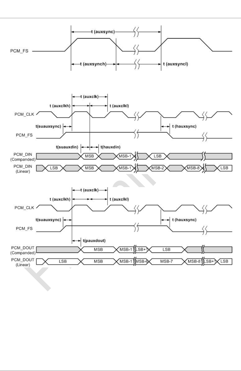
41124764188 Rev 0.41 March 20, 2013 47
Product Technical Specification
Figure 21. PCM_FS Timing Diagram (128 kHz Clock)
Figure 22. PCM Codec to AR Device Timing Diagram (Auxiliary PCM)
Figure 23. AR Device to PCM Codec Timing Diagram (Auxiliary PCM)
6.15.2.2. I2S
The AirPrime AR7550 I2S interface can be used to transfer serial digital audio to/from an external
stereo DAC/ADC. The I2S interface is a 4-wire interface: serial clock (I2S_SCLK), word select
(I2S_WS), serial uplink data (I2S_DIN), and serial downlink data (I2S_DOUT).
The AirPrime AR7550 I2S interface can be configured as a master or slave and either transmitter or
receiver.
A high-level timing diagram of the I2S signals is presented below.
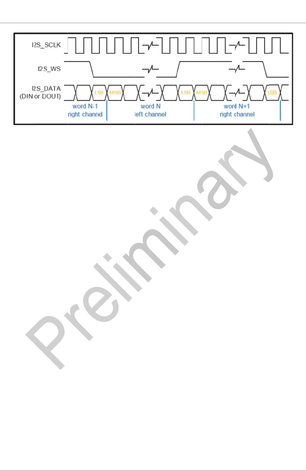
411247641
8
Product T
e
Figure 24.
6.15.2
.
The seri
I2S_DO
comple
m
length:
6.15.2
.
The wo
r
6.15.2
.
This is t
h
Sample
8
8
e
chnical Spe
c
I2S Signals
T
.
2.1.
i
al PCM ster
e
UT signal pi
n
m
ent, with th
When the tr
a
receiver’s L
S
When the tr
a
LSB will be
s
The MSB h
a
The transmi
t
Serial data
s
leading (L-t
o
Serial data
m
.
2.2.
r
d-select line
0 specifies t
1 specifies t
The WS sig
n
.
2.3.
h
e serial bit
c
I2S_SCLK
Where bit_
w
I2S_SCLK
rates of 8, 1
I2S_SCLK
Where bit_
w
c
ification
T
iming Diagra
m
I2S_DIN
a
e
o-data stre
a
n
and input
o
e MSB first.
a
nsmitted w
o
S
B are ignor
a
nsmitted w
o
s
et to zero i
n
a
s a fixed po
t
ter always
s
s
ent by the t
r
o
-H) edge of
m
ust be latc
h
I2S_WS
indicates th
he left chan
n
he right cha
n
n
al changes
I2S_SCL
K
c
lock whose
rate = (2
w
idth = 16 bi
t
rate = 32
6, 24, 32, 4
4
rate = (2
w
idth = 16 a
n
Rev 0.41
m
a
nd I2S_D
a
m for both
c
o
n the I2S_
D
The transmi
t
o
rd length is
e
d; the rest
o
o
rd length is
n
itially, so th
e
s
ition, wher
e
s
ends the M
S
r
ansmitter m
the clock si
g
h
ed into the
r
e channel b
e
n
el
n
nel
one clock p
e
K
rate is a fu
n
x bit_w
i
t
s per chann
e
x FS
4
.1, and 48
k
x 16) x
n
d FS = 48 k
H
OUT
c
hannels ar
e
D
IN signal pi
n
t
ter and rec
e
greater tha
n
o
f the trans
m
less than th
e
e
y will remai
e
as the LSB
S
B of the ne
x
ay be synch
g
nal.
r
eceiver on
t
e
ing transmi
t
e
riod before
n
ction of the
d
i
dth) x F
S
e
l and FS is
k
Hz are sup
p
48 kHz =
H
z.
e
output fro
m
n
. Serial dat
a
e
iver are not
n
the receive
m
itter’s LSBs
e
receiver w
o
n at zero.
position de
p
x
t word one
c
ronized with
t
he leading
e
t
ted / receiv
e
the MSB is
t
d
ata width a
S
the sample
r
p
orted. An e
x
1.536 MH
z
March
2
m
the AirPrim
e
a
is transmit
t
required to
h
r
word lengt
h
are ignored
o
rd length, t
h
ends upon
w
c
lock period
either the tr
a
dge of the s
e
e
d:
t
ransmitted.
n
d sample r
a
r
ate, therefo
r
x
ample clock
z
2
0, 2013
e AR7550 o
n
t
ed in two’s
h
ave the sa
m
h
, the bits af
t
.
h
e receiver’
s
w
ord length.
after WS ch
a
iling (H-to-
L
erial clock si
a
te:
r
e:
k
rate is:
4
8
n
the
m
e word
t
er the
s
missing
anges.
L
) or
gnal.
8
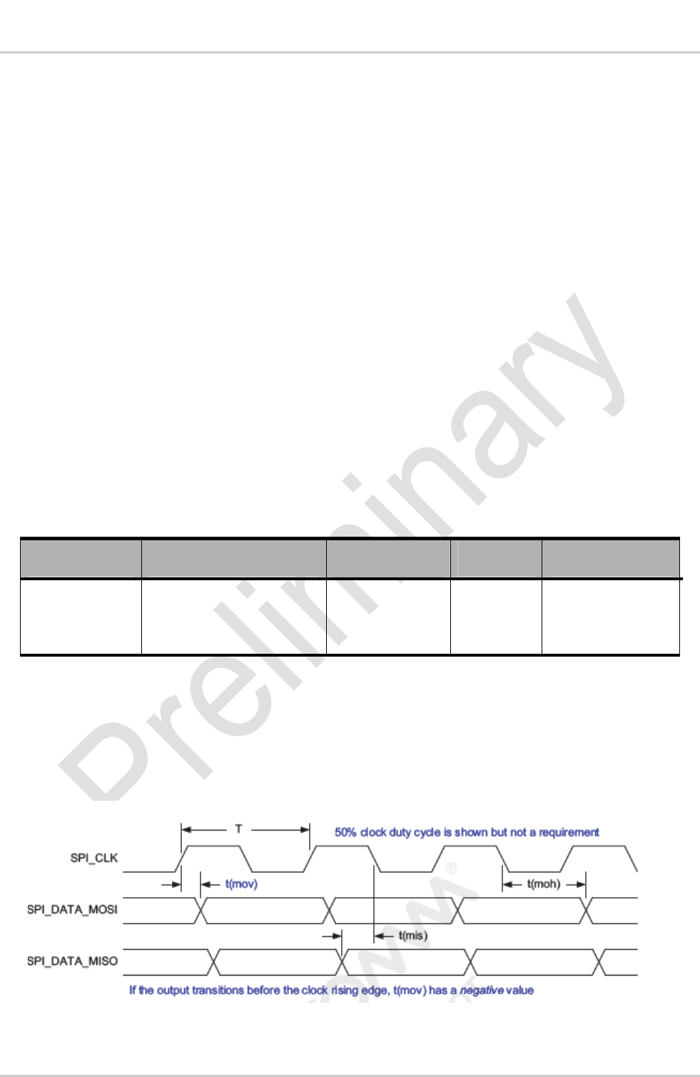
41124764188 Rev 0.41 March 20, 2013 49
Product Technical Specification
6.16. SPI Bus
The AirPrime AR7550 embedded module provides one SPI bus (4-wire interface).
SPI bus interface includes:
A CLK signal
An O signal
An I signal
A CS (Chip Select) signal
6.16.1. Characteristics
The following features are available on the SPI bus:
Master-only mode operation
SPI speed is from 128 kbit/s to 26 Mbit/s in master mode operation
4-wire interface
4 to 32 (TBD) bits data length.
6.16.2. SPI Configuration
Table 62. SPI Configuration
Operation Maximum Speed SPI-Mode Duplex 4-wire Type
Master 26Mb/s 0,1,2,3 full
SPIx-CLK;
SPIx-IO;
SPIx-I;
SPIx_CS
For the 4-wire configuration, SPIx-I/O is used as output only, SPIx-I is used as input only (TBC by
firmware).
6.16.3. SPI Waveforms
The following figure shows waveforms for SPI transfer with 4-wire configuration.
Figure 25. 4-Wire Configuration SPI Transfer
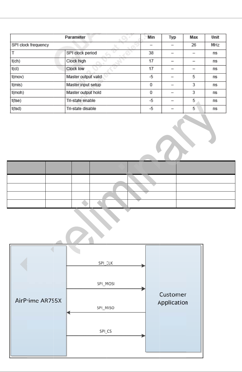
411247641
8
Product T
e
Table 63.
6.16.
Refer to
Table 64.
Signal
SPI-CLK
SPI-MIS
O
SPI-MO
S
SPI_CS
6.16.
A 4-wir
e
Figure 26.
8
8
e
chnical Spe
c
SPI Master
T
4. SPI
the followin
g
SPI Pin Des
Pi
n
C
E
O
C
E
S
I
C
D
C
D
5. Ap
p
e
SPI config
u
Example of
4
c
ification
T
iming Chara
c
Pin De
g
table for t
h
cription
n
#
I/
O
E
4
O
E
3
I
D
4
O
D
5
O
p
licatio
n
u
ration has t
h
4
-wire SPI Bus
A
Rev 0.41
c
teristics
scripti
o
h
e SPI interf
a
O
I/O Ty
p
1V8
1V8
1V8
1V8
n
h
e input and
A
pplication
o
n
a
ce pin desc
r
p
e
R
Z
Z
Z
Z
output data
r
iption.
R
eset State
lines disass
o
March
2
De
s
SPI
SPI
SPI
SPI
o
ciated.
2
0, 2013
s
cription
Serial Clock
Serial input
Serial output
Chip Select
5
0
0
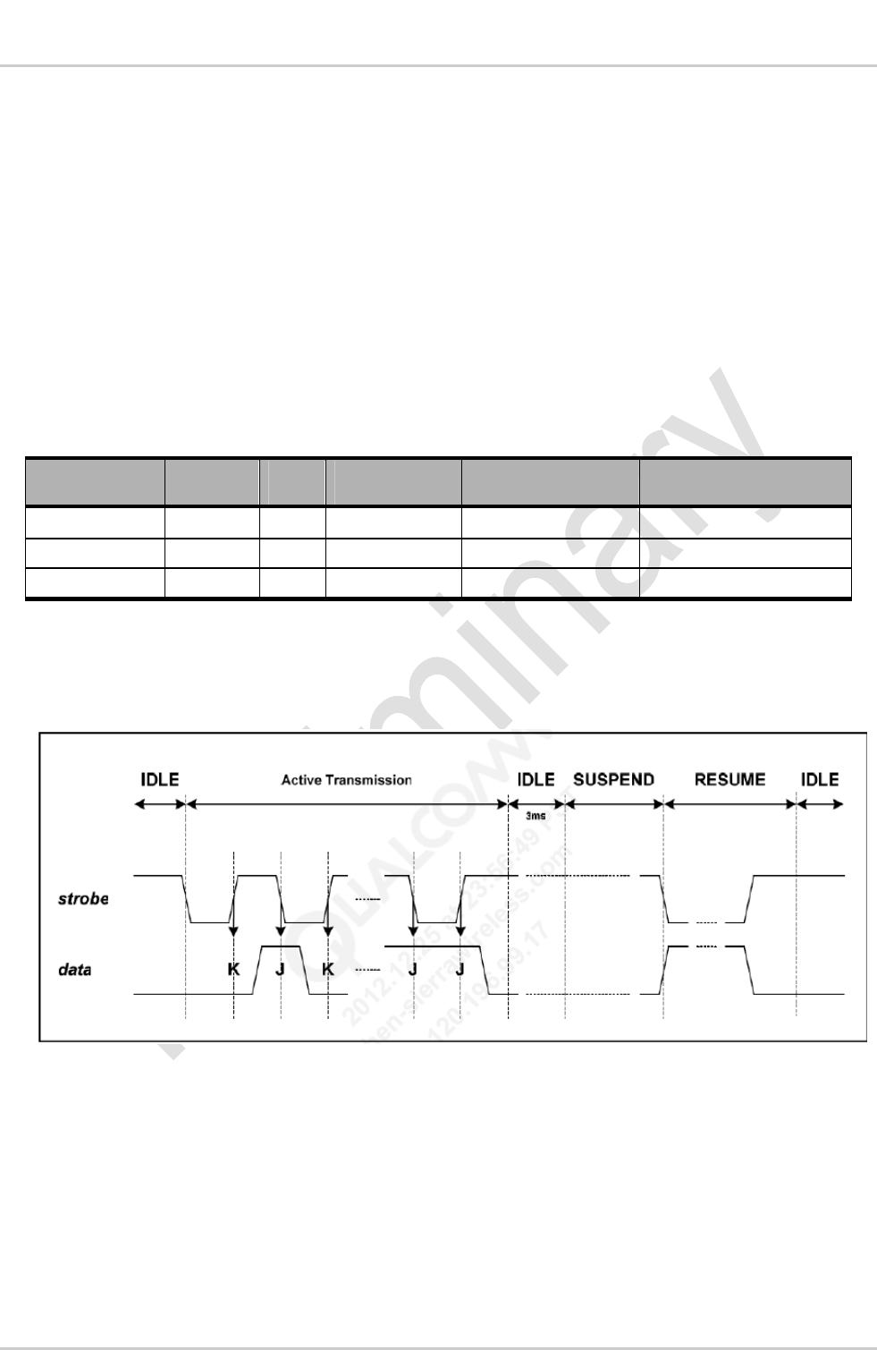
41124764188 Rev 0.41 March 20, 2013 51
Product Technical Specification
6.17. HSIC Bus
The AirPrime AR7550 embedded module provides one HSIC bus (2-wire interface).
HSIC bus interface includes:
HSIC strobe signal
HSIC data signal
Calibration pad for HSIC port signal
6.17.1. HSIC Pin Description
Refer to the following table for the HSIC interface pin description.
Table 65. HSIC Pin Description
Signal Pin # I/O I/O Type Reset State Description
HSIC_STB AA2 B 1V2 Z HSIC strobe signal
HSIC_DATA AA3 B 1V2 Z HSIC data
HSIC_CAL AA4 B 1V2 Z HSIC calibration pad
6.17.2. HSIC Waveforms
The following figure shows waveforms for HSIC signal sample.
Figure 27. HSIC Signal Sample Waveforms
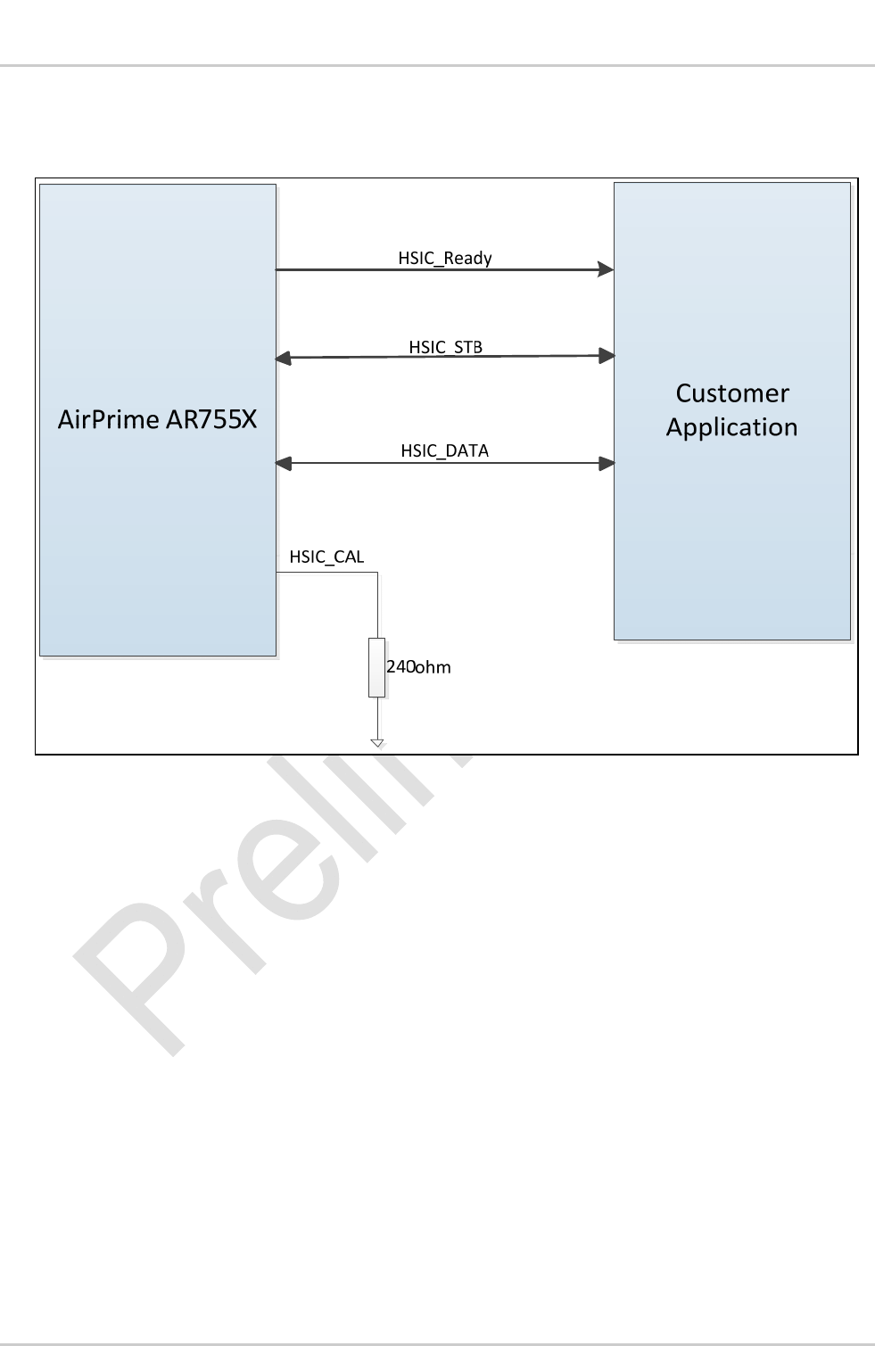
41124764188 Rev 0.41 March 20, 2013 52
Product Technical Specification
6.17.3. Application
A 4-wire SPI configuration has the input and output data lines disassociated.
Figure 28. Example of HSIC Bus Application
Note 1: Trace length to 10cm maximum
2: Skew between data and strobe signals < 15ps, and
3: Connect HSIC_Ready to HSIC_RST_N of the HSIC device.
41124764188 Rev 0.41 March 20, 2013 53
Product Technical Specification
6.18. Temperature Monitoring
The AirPrime AR7550 has internal temperature monitoring of both the PMIC device and the Power
Amplifier devices.
Normal High Temperature
Warning
Power off.
Handled by
Power State
state machine.
High Temperature
Critical
(Low power mode)
Low Temperature
Critical
(Low power mode)
current_temp < TEMP_HI_WARN
current_temp < TEMP_LO_CRIT
current_temp > TEMP_NORM_LO
current_temp > TEMP_HI_CRIT
Application asserts ON/OFF
Or
Issues AT!POWERDOWN
Application asserts ON/OFF
Or
Issues AT!POWERDOWN
current_temp > TEMP_HI_WARN
current_temp < TEMP_HI_NORM
Figure 29. Temperature Monitoring State Machine
Table 66. Temperature Monitoring States
State Description Threshold1 Default Temp
value (°C) Functionality
Normal
Both PMIC and PA
Thermistors are
between
TEMP_HI_NORM +85
All
TEMP_LO_NORM -40
High
Temperature
Warning
Either PMIC or PA
Thermistor has
exceeded
TEMP_HI_WARN +95
All –
Warning message output
on AT Command port
High
Temperature
Critical
Either PMIC or PA
Thermistor has
exceeded
TEMP_HI_CRIT 140
Low Power Mode – Device
will only make Emergency
calls
Low
Temperature
Critical
Either PMIC or PA
Thermistor has
descended past
TEMP_HI_CRIT -45
Low Power Mode – Device
will only make Emergency
calls
1 There are two sets of thresholds: PATEMP for PA Thermistor, and PCTEMP for PMIC Thermistor.
To restore full operation, temperature readings for both the PA and PMIC Thermistors must be within
the Normal or High Temperature Warning state thresholds.
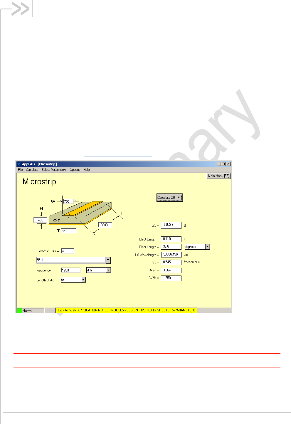
4112476 Rev 0.4 March 20, 2013 54
7. Routing Constraints and
Recommendations
Layout and routing of the AirPrime AR7550 device in the application is critical to maintaining the
performance of the radio. The following sections provide guidance to the developer when designing
their application to include an AirPrime AR7550 device and achieve optimal system performance.
7.1. RF Routing Recommendations
To route the RF antenna signals, the following recommendations must be observed for PCB layout:
The RF signals must be routed using traces with a 50 characteristic impedance.
Basically, the characteristic impedance depends on the dielectric constant (εr) of the material used,
trace width (W), trace thickness (T), and height (H) between the trace and the reference ground plane.
In order to respect this constraint, Sierra Wireless recommends that a MicroStrip structure be used
and trace width be computed with a simulation tool (such as AppCAD, shown in the figure below and
available free of charge at http://www.avagotech.com).
Figure 30. AppCAD Screenshot for Microstrip Design Power Mode Diagram
The trace width should be wide enough to maintain reasonable insertion loss and manufacturing
reliability. Cutting out inner layers of ground under the trace will increase the effective substrate
height; therefore, increasing the width of the RF trace.
Caution: It is critical that no other signals (digital, analog, or supply) cross under the RF path. The figure
below shows a generic example of good and poor routing techniques.
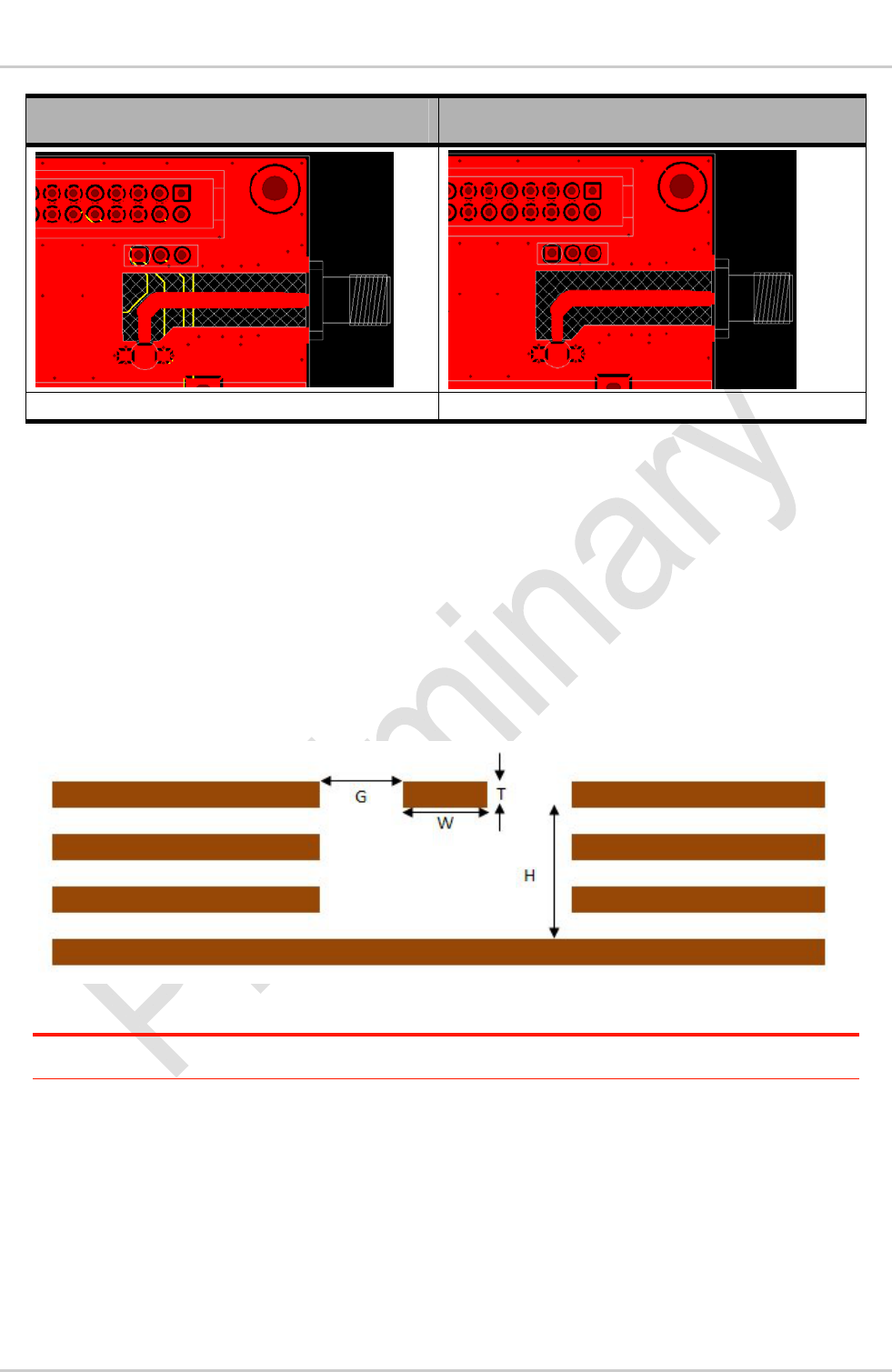
41124764188 Rev 0.41 March 20, 2013 55
Product Technical Specification
Poor routing Correct routing
The yellow traces cross the RF trace. There is no signal around the RF path.
Figure 31. RF Routing Examples
Fill the area around the RF traces with ground and ground vias to connect inner ground layers
for isolation.
Cut out ground fill under RF signal pads to reduce stray capacitance losses.
Avoid routing RF traces with sharp corners. A smooth radius is recommended.
E.g. Use of 45° angles instead of 90°.
The ground reference plane should be a solid continuous plane under the trace.
The coplanar clearance (G, below) from the trace to the ground should be at least the trace
width (W) and at least twice the height (H). This reduces the parasitic capacitance, which
potentially alters the trace impedance and increases the losses.
E.g. If W = 100 microns then G = 200 microns in an ideal setup. G = 150 microns would also
be acceptable is space is limited.
Figure 32. Coplanar Clearance Example
Note: The figure above shows several internal ground layers cut out, which may not be necessary for
every application.

41124764188 Rev 0.41 March 20, 2013 56
Product Technical Specification
Figure 33. Antenna Microstrip Routing Example
7.2. Power and Ground Recommendations
Power and ground routing is critical to achieving optimal performance of the AirPrime AR7550 devices
when integrated into an application.
Recommendations:
Do not use a separate GND for the Antennas
Connections to GND from the AirPrime AR7550 should be flooded plane using thermal reliefs
to ensure reliable solder joints.
VBATT is recommended to be routed as a wide trace(s) directly from the 4V supply to the
LGA pad.
7.3. Antenna Recommendations
The AirPrime AR7550 devices are designed to provide diagnostics status of the antennas connected
to it.
The Primary antenna interface is optimized for a multiband cellular antenna with a 10 k DC
impedance between the antenna element and the ground reference.
The GNSS antenna interface is optimized for a 5V active GNSS antenna supporting the GPS
L1 and GLONASS L1 FDMA bands. Refer to the GNSS Antenna Diagnostics section.
Connecting the antenna ground reference to the vehicle chassis is not recommended since that has
been known to cause noise from the engine to couple into the audio of the device. It is ultimately up to
the integrator to evaluate this performance.
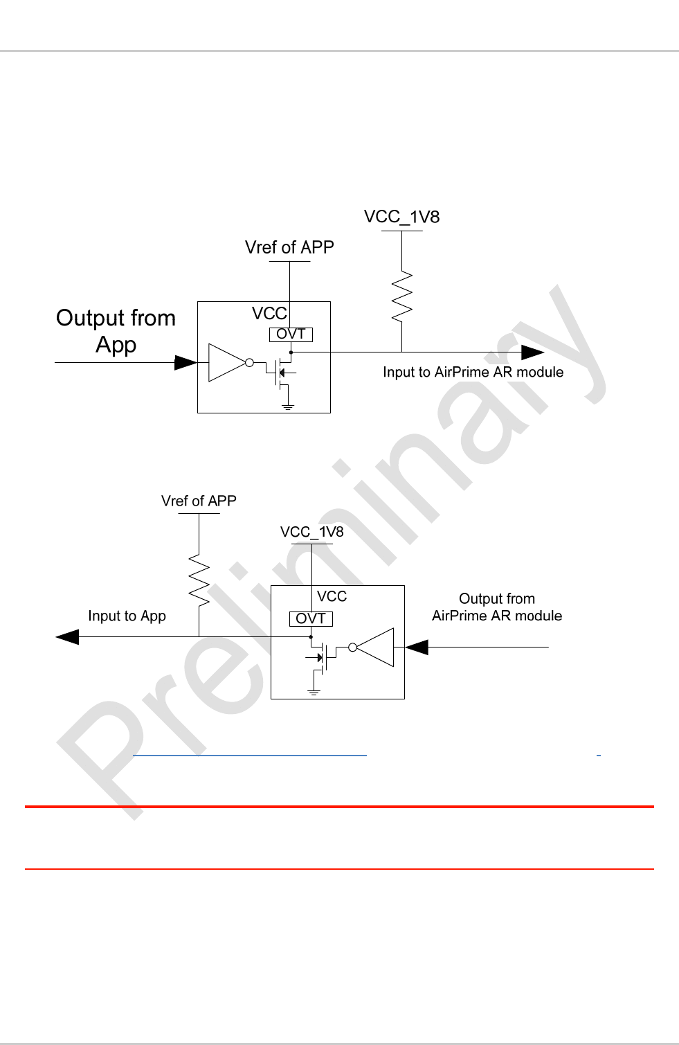
41124764188 Rev 0.41 March 20, 2013 57
Product Technical Specification
7.4. Interface Circuit Recommendations
The recommended interface implementation is to use open-drain non-inverting buffers with pull-ups to
the appropriate voltage reference. This allows a host processor operating at a different voltage to
communicate with the AirPrime AR7550 using the appropriate voltage levels.
The figure below is a reference circuit for a digital input signal to the AirPrime AR7550 device.
Figure 34. AirPrime AR7550 Input Reference Circuit
The figure below is a reference circuit for a digital output signal from the AirPrime AR7550 device.
Figure 35. AirPrime AR7550 Output Reference Circuit
Refer to Chapter Error! Reference source not found. Error! Reference source not found. section
to identify the appropriate reference voltage and direction of the specific signals.
The open-drain non-inverting buffer used in the reference circuits above is the OnSemi NL17SZ07.
Tip: The NL17SZ07 is over-voltage tolerant on the inputs. It may be possible to power all the buffers
from the 1.8V reference voltage output. Review the digital output characteristics of the applications
drivers and the Input characteristics of the buffer selected to determine if this would work in your
application.
If a Digital IO signal is used bidirectional in the application then a bidirectional buffer or bidirectional
level translator is needed.

4112476 Rev 0.4 March 20, 2013 58
8. Regulatory Information
8.1. Important Notice
Because of the nature of wireless communications, transmission and reception of data can never be
guaranteed. Data may be delayed, corrupted (i.e., have errors) or be totally lost.
Although significant delays or losses of data are rare when wireless devices such as the Sierra
Wireless modem are used in a normal manner with a well-constructed network, the Sierra Wireless
modem should not be used in situations where failure to transmit or receive data could result in
damage of any kind to the user or any other party, including but not limited to personal injury, death,
or loss of property. Sierra Wireless and its affiliates accept no responsibility for damages of any kind
resulting from delays or errors in data transmitted or received using Sierra Wireless modem, or for
failure of the Sierra Wireless modem to transmit or receive such data.
Safety and Hazards
Do not operate the AR7550 modem:
In areas where blasting is in progress
Where explosive atmospheres may be present including refueling points, fuel depots, and
chemical plants
Near medical equipment, life support equipment, or any equipment which may be susceptible
to any form of radio interference. In such areas, the AR Series device MUST BE POWERED
OFF. Otherwise, the AR Series device can transmit signals that could interfere with this
equipment
In an aircraft, the AR Series device MUST BE POWERED OFF. Otherwise, the AR Series
device can transmit signals that could interfere with various onboard systems and may be
dangerous to the operation of the aircraft or disrupt the cellular network. Use of cellular phone
in aircraft is illegal in some jurisdictions. Failure to observe this instruction may lead to
suspension or denial of cellular telephone services to the offender, or legal action or both.
Some airlines may permit the use of cellular phones while the aircraft is on the ground and
the door is open. The AR Series device may be used normally at this time.
8.2. Important Compliance Information for USA
OEM Integrators
The AR Series device is granted with a modular approval for mobile applications. Integrators may use
the AR Series device in their final products without additional FCC/IC (Industry Canada) certification if
they meet the following conditions. Otherwise, additional FCC/IC approvals must be obtained.
1. At least 20cm separation distance between the antenna and the user’s body must be
maintained at all times.
2. To comply with FCC/IC regulations limiting both maximum RF output power and human
exposure to RF radiation, the maximum antenna gain including cable loss in a mobile-only
exposure condition must not exceed the gain values presented in the table below:
6.5 dBi in Cellular band
3 dBi in PCS band
6.0 dBi in LTE Band 4
9.0 dBi in LTE Band 7
9.0 dBi in LTE Band 13 (Note: LTE Band 13 is not permitted in Canada.)
41124764188 Rev 0.41 March 20, 2013 59
Product Technical Specification
3. The AR7550 modem may transmit simultaneously with other collocated radio transmitters
within a host device, provided the following conditions are met:
Each collocated radio transmitter has been certfied by FCC / IC for mobile application.
At least 20 cm separation distance between the antennas of the collocated transmitters
and the user’s body must be maintained at all times.
The output power and antenna gain must not exceed the limits and configurations
stipulated in the following table.
Device Technology Band Frequency
(MHz)
Maximum
conducted power Maximum antenna
gain
AR7550
Module
LTE 4 1710-1755 24 6
7 2500 – 2570 24 9
13 777-787 24 6
UMTS 2 1850-1910 24 3
5 824-849 24 3
CDMA BC0 824-849 25 3
BC1 1850-1910 25 3
Collocated
transmitters1
WLAN 2400-2500 29 5
5150-580 29 5
WiMAX 2300-2400 29 5
2500-2700 29 5
3300-3800 29 5
BT 2400-2500 15 5
1. Valid collocated Transmitter combinations: WLAN+BT; WiMAX+BT.
(WLAN+WiMAX+BT is not permitted.)
4. A label must be affixed to the outside of the end product into which the AirPrime AR7550
device is incorporated, with a statement similar to the following:
a.
This device contains FCC ID: N7NAR7550
This equipment contains equipment certified under IC: 2417C-AR7550
A user manual with the end product must clearly indicate the operating requirements and conditions
that must be observed to ensure compliance with current FCC/IC RF exposure guidelines.
The end product with an embedded AirPrime AR7550 device may also need to pass the FCC Part 15
unintentional emission testing requirements and be properly authorized.
Note: If this module is intended for use in a portable device, you are responsible for separate approval to
satisfy the SAR requirements of FCC Part 2.1093 and IC RSS-102.
4112476 Rev 0.4 March 20, 2013 60
9. References
The table below lists the reference specifications for this product.
Table 67. Reference Specifications
Ref Title Issuer
[1] Recommended Minimum Performance Standards for
cdma2000 High Rate Packet Data Access Terminal – C.S0033 3GPP2
[2] Recommended Minimum Performance Standards for
cdma2000 Spread Spectrum Mobile Stations – C.S0011 (IS-98D) 3GPP2
[3] Universal Serial Bus Specification USB Implementers
Forum
[4] Universal Serial Bus CDC Subclass Specification for Wireless Mobile
Communication Devices
USB Implementers
Forum
[5] Universal Serial Bus Class Definitions for Communication Devices USB Implementers
Forum
[6] AirPrime AR Series Customer Process Guidelines Sierra Wireless
[7] AirPrime AR7 Series AT Command Interface Specification Sierra Wireless
[8] AirPrime AR7 Series Firmware Download Guide Sierra Wireless
4112476 Rev 0.4 March 20, 2013 61
10. Abbreviations
The table below lists several abbreviations used in this document.
Table 68. Abbreviations
Abbreviation Description
CDMA Code Division Multiple Access
DRX Discontinuous Receive
GNSS Global Navigation Satellite System
GSM Global System for Mobile Communications
HSPA High Speed Packet Access
LTE Long Term Evolution
SCI Slot Cycle Index
USB Universal Serial Bus
WCDMA Wideband Code Division Multiple Access
WWAN Wireless Wide Area Network