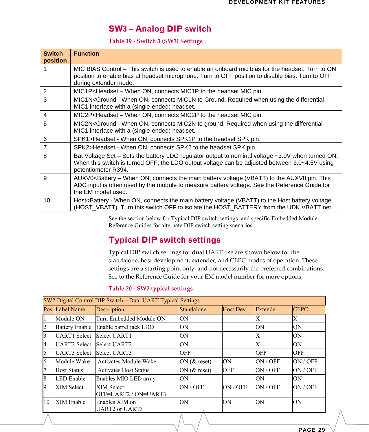
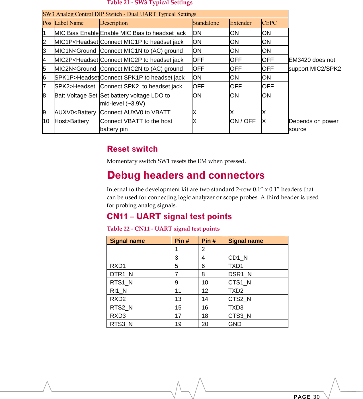
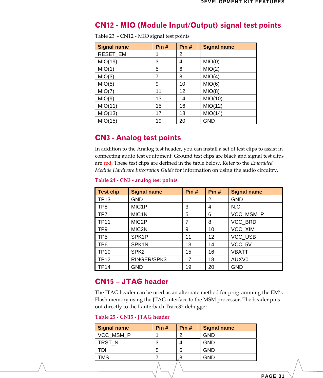
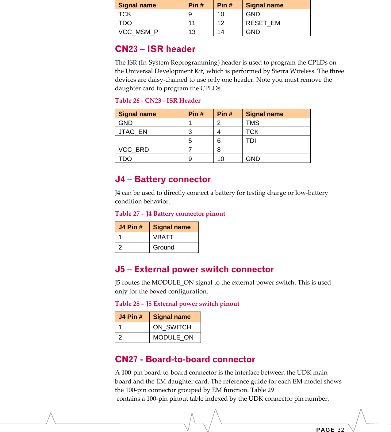
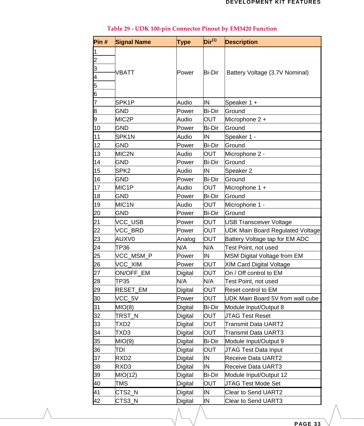
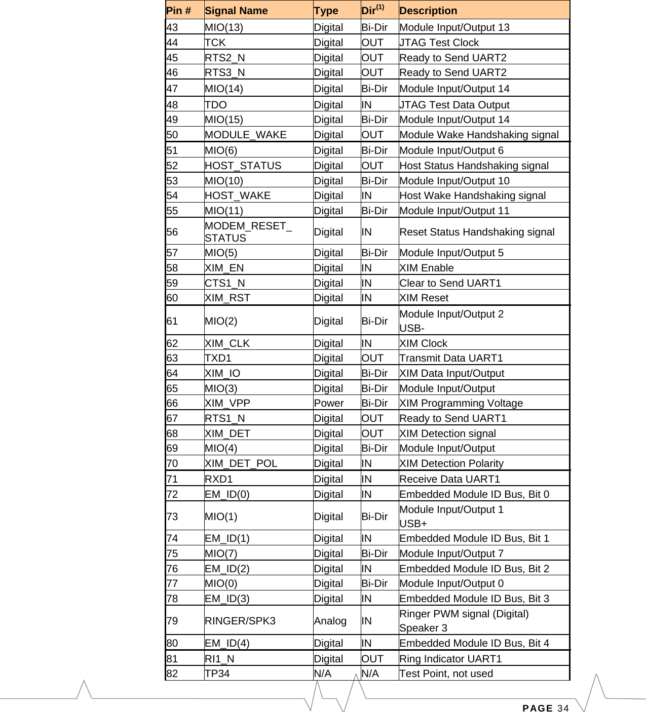
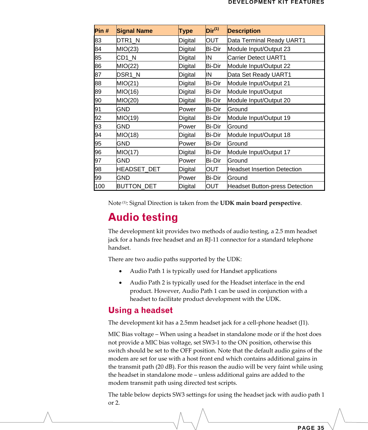
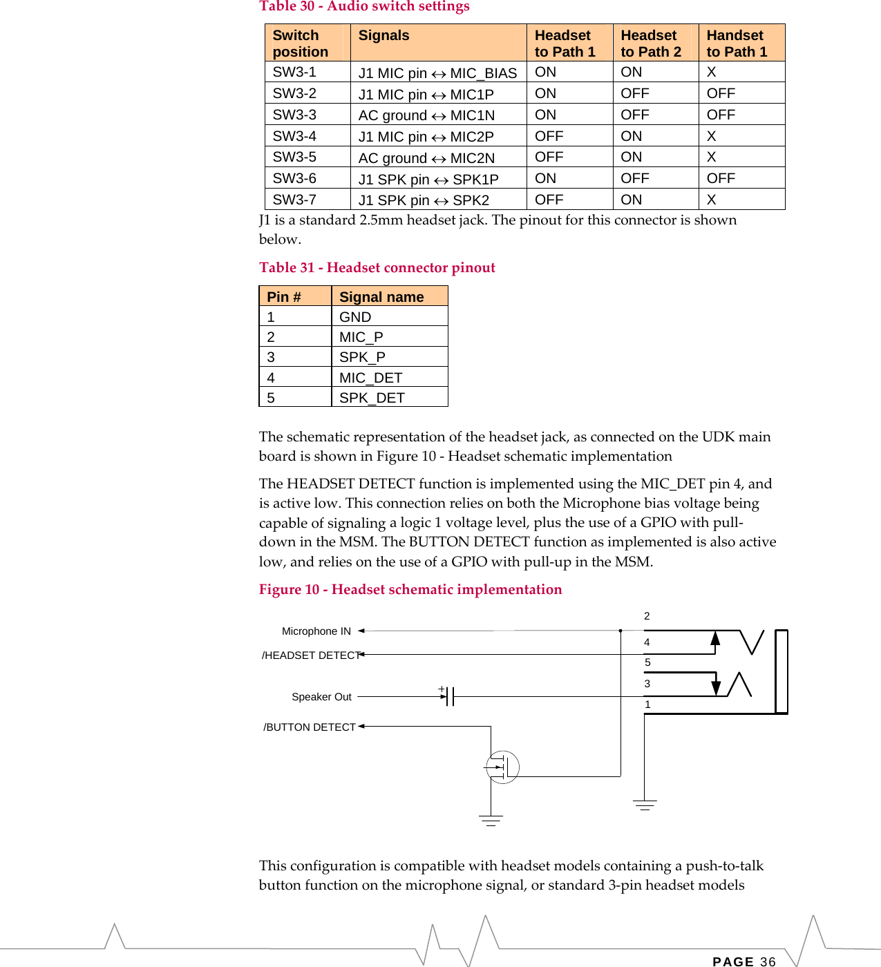
Sierra Wireless EM5625 Embedded Wireless Radio Modem User Manual Universal Development Kit Hardware Users Guide

Sierra Wireless Inc. Embedded Wireless Radio Modem Universal Development Kit Hardware Users Guide

User Manual

     Universal Development Kit  Hardware Users Guide                             2130391 Rev 1.1
UNIVERSAL DEVELOPMENT KIT SierraWirelessreservestherighttomakechangesinitsproductswithoutnoticeinordertoimprovedesignorperformancecharacteristics.Thispublicationneitherstatesnorimpliesanywarrantyofanykind,includingbutnotlimitedtoimpliedwarrantsofmerchantabilityorfitnessforaparticularapplication.Theinformationinthispublicationisbelievedtobeaccurateinallrespectsatthetimeofpublication,butissubjecttochangewithoutnotice.SierraWirelessassumesnoresponsibilityforanyerrororomissions,anddisclaimsresponsibilityforanyconsequencesresultingfromtheuseoftheinformationincludedherein.Copyright©2004 SierraWireless.Allrightsreserved.  PAGE 2
  INTRODUCTION Table of Contents  INTRODUCTION......................................................................................................................... 6 OVERVIEW ................................................................................................................................... 6 TERMS AND ACRONYMS .............................................................................................................. 6 REGULATORY INFORMATION............................................................................................. 7 STATEMENT ................................................................................................................................. 7 REQUIREMENTS............................................................................................................................ 7 SAFETY ........................................................................................................................................ 7 User operation requirements.................................................................................................. 7 INTERFACES ................................................................................................................................. 8 DEVELOPMENT KIT CONTENTS .................................................................................................... 9 CONFIGURATIONS ........................................................................................................................ 9 Boxed configuration................................................................................................................ 9 Bench configuration.............................................................................................................. 10 SETUP AND INSTALLATION ................................................................................................ 12 QUICK SETUP ............................................................................................................................. 12 PC CONNECTIONS ...................................................................................................................... 12 POWERING THE DEVELOPMENT KIT ........................................................................................... 13 AC wall cube power.............................................................................................................. 13 DC power.............................................................................................................................. 14 RF CONNECTION ....................................................................................................................... 14 DEVELOPMENT KIT FEATURES ........................................................................................ 16 INTRODUCTION .......................................................................................................................... 16 MODES OF OPERATION ............................................................................................................... 16 Standalone mode................................................................................................................... 16 Host Development mode ....................................................................................................... 17 Extender Mode...................................................................................................................... 18 CEPC mode........................................................................................................................... 19 LED INDICATORS ...................................................................................................................... 21 D10 – 10-segment LED......................................................................................................... 21 D11 – Board power LED...................................................................................................... 22 D12 – Module power LED.................................................................................................... 22 SERIAL INTERFACES................................................................................................................... 23 UART (1~3) - DE9................................................................................................................ 23 UART signals ........................................................................................................................ 23 UART switches...................................................................................................................... 23 UART monitor support.......................................................................................................... 24 XIM interface........................................................................................................................ 26 USB ....................................................................................................................................... 27 SWITCHES .................................................................................................................................. 27 SW2 – Digital control DIP switch ........................................................................................ 27  PAGE 3
  SW3 – Anlalog DIP switch.................................................................................................... 29 Typical DIP switch settings .................................................................................................. 29 Reset switch........................................................................................................................... 30 DEBUG HEADERS AND CONNECTORS .......................................................................................... 30 CN11 – UART signal test points........................................................................................... 30 CN12 - MIO (Module Input/Output) signal test points......................................................... 31 CN3 - Analog test points....................................................................................................... 31 CN15 – JTAG header............................................................................................................ 31 CN23 – ISR header ............................................................................................................... 32 J4 – Battery connector.......................................................................................................... 32 J5 – External power switch connector.................................................................................. 32 CN27 - Board-to-board connector........................................................................................ 32 AUDIO TESTING.......................................................................................................................... 35 Using a headset..................................................................................................................... 35 Using a handset..................................................................................................................... 37 RF INTERFACE......................................................................................................................... 38 INTRODUCTION .......................................................................................................................... 38 50Ω CONNECTION ..................................................................................................................... 38 Cables ................................................................................................................................... 39 ANTENNA USE............................................................................................................................ 39 PART NUMBERS.......................................................................................................................... 39 Figures Figure 1 - UDK boxed Configuration........................................................................................... 10 Figure 2 - UDK bench configuration............................................................................................ 11 Figure 3 - Dual UART and USB+UART Configurations............................................................. 12 Figure 4 - RF Connections Diagram............................................................................................ 15 Figure 5 - Standalone mode connection diagram......................................................................... 17 Figure 6 - Extender mode configuration ...................................................................................... 19 Figure 7 – CEPC connection diagram ......................................................................................... 20 Figure 8 - Monitor mode connection example.............................................................................. 25 Figure 9 - Protocol analyzer Y-adapter cable.............................................................................. 26 Figure 11 - Headset schematic implementation ........................................................................... 36 Figure 12 - Pushbutton microphone headset................................................................................ 37 Tables Table 1 – Acronyms and definitions................................................................................................ 6 Table-2 - UDK Interfaces ............................................................................................................... 8 Table 3 - Power switch settings .................................................................................................... 13 Table 4 - VBATT voltage adjustment............................................................................................ 14 Table 5 – Standalone / Host Development mode switch configurations ...................................... 18 Table 6 - Extender mode switch configuration............................................................................. 18 Table 7 - CEPC switch settings .................................................................................................... 19 Table 9 - CEPC Signal Definition ................................................................................................ 20 Table 10 - Primary 10-segment LED map.................................................................................... 21   PAGE 4
  INTRODUCTION Table 11 - Secondary 10-segment LED map ................................................................................ 22 Table 12 - D12 power LED states................................................................................................. 22 Table 13 - UART signals............................................................................................................... 23 Table 14 - UART Switch Settings.................................................................................................. 23 Table 15 - UART Monitor Connections........................................................................................ 24 Table 16 - XIM switch settings...................................................................................................... 26 Table 17 - CN25 XIM signal interface.......................................................................................... 27 Table 18 - USB signal interface.................................................................................................... 27 Table 19 - Switch 2 (SW2) settings ............................................................................................... 28 Table 20 - Switch 3 (SW3) Settings............................................................................................... 29 Table 21 - SW2 typical settings..................................................................................................... 29 Table 22 - SW3 Typical Settings................................................................................................... 30 Table 23 - CN11 - UART signal test points .................................................................................. 30 Table 24  - CN12 - MIO signal test points.................................................................................... 31 Table 25 - CN3 - analog test points.............................................................................................. 31 Table 26 - CN15 - JTAG header................................................................................................... 31 Table 27 - CN23 - ISR Header...................................................................................................... 32 Table 28 – J4 Battery connector pinout........................................................................................ 32 Table 29 – J5 External power switch pinout ................................................................................ 32 Table 30 - UDK 100-pin Connector Pinout by EM3420 Function............................................... 33 Table 31 - Audio switch settings................................................................................................... 36 Table 32 - Headset connector pinout............................................................................................ 36 Table 33 - Handset connector pinout............................................................................................ 37 Table 34 - Typical RF Performance Parameters.......................................................................... 38 Table 35 - Connector part numbers.............................................................................................. 39  PAGE 5
  Introduction Overview ThisdocumentexplainsthefeaturesandcapabilitiesoftheUniversalDevelopmentKit(UDK).TheUDKisbasedonadevelopmentplatformthatisdesignedtosupportmultiplemembersoftheWirelessEmbeddedModule(EM)productfamily.ThepurposeoftheUniversalDevelopmentKitistoassisttheOEMduringthefollowingproductdevelopmentstages:•  InitialEMevaluation•  Hostsoftwaredevelopment•  PreliminaryhardwareintegrationTerms and Acronyms Table1–AcronymsanddefinitionsAcronym or Term  Definition Call Box  Test equipment used for CDMA testing, a.k.a. test set CDMA  Code Division Multiple Access (digital phone standard) Cellular  800 MHz radio spectrum air interface CW Clock-wise CCW Counter clock-wise dB  Decibel = 10 x log10 (P1/P2) (Power dB) Decibel = 20 x log10 (V1/V2) (Voltage dB) dBm   Decibels, relative to 1 mW… Decibel(mW) = 10 x log10 (Pwr (mW)/1mW) EM Embedded Module GPS  Global positioning system HW Hardware MIO Module Input/Output Modem  Modulator – demodulator (the EM) PCS  Personal Communication System –spans the 1.9GHz radio spectrum RF Radio Frequency RUIM  Removable User Identity Module SIM  Subscriber Identity Module UART  Universal Asynchronous Receiver Transmitter UDK Universal Development Kit USB  Universal Serial Bus xIM  Either RUIM or SIM, as the cards themselves are interchangeable   PAGE 6
  REGULATORY INFORMATION Regulatory Information Statement Thefollowingsafetyprecautionsmustbeobservedduringallphasesoftheoperation,use,serviceorrepairofanycellularterminalormobileincorporatingtheEM.Manufacturersofthecellularterminaldevicesareadvisedtoconveythefollowingsafetyinformationtousersandoperatingpersonnelandtoincorporatetheseguidelinesintoallsafetystandardsofdesign,manufactureandintendeduseoftheproduct.SierraWirelessassumesnoliabilityforcustomerfailuretocomplywiththeseprecautions.1.TheEMmustbeoperatedatthevoltagesdescribedinthistechnicaldocumentation.2.TheEMmustnotbemechanicallyorelectricallychanged.Useoftheconnectorsshouldfollowtheguidanceofthistechnicaldocumentation.3.TheEMisdesignedtomeettheEMCrequirementsof47CFRPart2andPart15.4.WhenintegratingtheEMintoasystem,SierraWirelessrecommendstestingthesystemtoOETBulletin65SupplementCedition97‐01.Requirements TheFederalCommunicationsCommission(FCC)requiresapplicationforcertificationofdigitaldevicesinaccordancewithCFRTitle47,Part2andPart15.Thisincludeselectromagneticsusceptibilitytesting.AstheEMisnotastand‐alonetransceiverbutisanintegratedmodule,theEMcannotbetestedbyitselfforEMC/EMIcertification.ThisdevicecomplieswithPart15oftheFCCrules.OperationoftheEMissubjecttothefollowingtwoconditions:(1)thisdevicemaynotcauseharmfulinterference,and(2)thisdevicemustacceptanyinterferencereceived,includinginterferencethatmaycauseundesiredoperation.Yourmobiledeviceisalowpowerradiotransmitterandreceiver.WhileON,itreceivesandsendsoutradiofrequency(RF)signals.ThedesignofthismodulecomplieswiththeFCCguidelinesandapplicablestandards.WARNING:Unauthorizedantennas,modifications,orattachmentscouldimpaircallquality,damagetheEM,orresultinviolationofFCCregulations.DonotusetheEMwithadamagedantenna.Pleasecontactyourlocalauthorizeddealerforantennareplacement.Safety User operation requirements Theantennausedforthistransmittermustbeinstalledtoprovideaseparationdistanceofatleast20cmfromallpersonsandmustnotbeco‐locatedoroperatinginconjunctionwithanyotherantennasortransmitters.Apersonorobjectwithin8inches(20centimeters)oftheantennacouldimpaircallquality PAGE 7
  andmaycausethephonetooperateatahigherpowerlevelthannecessaryandexposethatpersontoRFenergyinexcessofthatestablishedbytheFCCRFExposureGuidelines.!IMPORTANT!:TheUDKmustbeinstalledwithaminimumseparationdistanceof20cmormorebetweentheantennaandpersonstosatisfyFCCRFexposurerequirementsformobiletransmittingdevices.Thetransmittereffectiveradiatedpowermustbelessthan1.5WattsERP,2.0Wattsor33.0dBmEIRP.Thisrequiresthatthecombinationofantennagainandfeedlinelossdoesnotexceed6.0dBi(Conductedmaxpower+cableloss+Antennagain).Interfaces TheUniversalDevelopmentKitconsistsoftwoprintedcircuitboards,amainboardandadaughtercard.ThemainboardcontainstheinterfacesanddevelopmentfeaturesthatarecommontomultipleEMtypes.ThedaughtercardisdesignedtoadaptagivenEMtypetothemainboard.Thefollowingtabledescribestheinterfacesanddevelopmentfeatures(mainboardonly)availableontheUniversalDevelopmentKit.Table-2 - UDK Interfaces External Interfaces   Available Outside of Box      USB connector: B-type / USB device    4  UART connectors: 2 or 3 UARTs + 1 or 2 TxD monitors      Power on/off switch      DC Input jack: +5VDC from universal input AC adapter    2 Power LEDs    10 Status LEDs     Reset switch      2.5mm headset jack      RJ-14 handset jack      Host adapter flat cable connector      RF connector for antenna or call-box: TNC female   Available on main board only      Battery test clips (& battery header)    2  Digital / Logic analyzer headers: GPIO & UART    1 Analog header      JTAG debug interface    2  x10 DIP switches: x10 analog / x10 digital     XIM socket   PAGE 8
  REGULATORY INFORMATION Development Kit Contents TheUniversalDevelopmentKitpackageincludes:•  UniversalDevelopmentKitmainboard•  UniversalDevelopmentKitdaughtercard•  WirelessEmbeddedModule(EM)•  Walloutlet110/220VACpowersupply•  2DE9serialcables•  CD‐ROMcontainingSierraWirelessToolssoftwareandutilitiesThekitalsoincludesanumberofoptionalcomponents,dependingontheEMtypeorintendeduse:•  Antenna–combinationsofcellular,PCSandGPSbandsuponrequest•  RFAdapter–specifictotheEMtype•  USBcable•  Parallelcable–onlyusedforCEPCinterface•  Headset–withpush‐to‐talkbutton•  DualUARTadapter–supports230kbps•  Metalenclosure–optional,typicallyusedfordemonstrationorcertificationConfigurations Boxed configuration Theboxed(demo)configurationisshownbelow.Youmustspecifythisdeliveryoptionatthetimeofordering.Notethatthisconfigurationisnotpreferablefordevelopmentuse,sinceonlyasubsetoftheinterfacesisavailable.ItisintendedforinitialEMevaluationordemonstrationonly.Thediagrambelowdepictsalloftheavailableinterfacesandindicatorsfortheboxedconfiguration,andisshownwiththelidoffforclarity.NotethattheinternalRFcableconnectseithertotheSMAortotheTNCbulkheadadapter,notboth. PAGE 9
  Figure1‐UDKboxedConfigurationTxDn See UART monitor support on page 24. USB.  See USB on page .27. UART1  See UART signals on page 23. UART2  See UART signals on page 23. UART3  See UART signals on page 23. TNC Adapter. (Typically not installed) See 50Ω Connection on page 38. SMA Adapter.  See 50Ω Connection on page 38. UDK Power LED. See D11– Board power LED on page 22. Module Power LED. See D12 –Module power LED on page 22. Wall Cube Input.  See AC wall cube power on page 13. Reset Button. See Reset switch on page 30. Headset Jack. See Using a headset on page 35. Handset Jack. See Using a handset on page 37. Bench configuration Thebenchconfigurationisthemostcommon‐usedconfiguration.Thisisanopen‐boardconfigurationwithaccesstoalldevelopmentfeatures.TheEM3420DaughterCardisshowninthediagramasanexample.Theembeddedmodule’sRFadaptercanalsobeaccesseddirectlyinthisconfigurationinordertominimizeRFlosses.TheseadditionalinterfacesareshowninFigure2‐UDKbenchconfiguration  PAGE 10
  SETUP AND INSTALLATION Figure2‐UDKbenchconfigurationCEPC / Parallel Interface. See page 19. EM RF Adapter. See page 38. SMA Adapter.  See page 38. EM3420 Daughter Card RUIM Connector. See page 24. Battery Header. See page  32. MIO Header See page 31. Digital / Control DIP Switch. See page 27. UART Header. See page 30. MSM JTAG Header. See page 31.Analog Header.  See page 31. Analog / Control DIP Switch. See page 29. CPLD Program Header. See page 32. 10x DIP LED. See page 21.  PAGE 11
   Setup and Installation Quick setup Tosetupandinstallthedevelopmentkit:1.ConfiguretheUDKDIPswitchesforStandaloneMode.SeeTypicalDIPswitchsettingsonpage29.Theboxedconfigurationhaspre‐configureddefaultsettings.2.ConnecttheDevelopmentKittoaPC(orotherhost)viaserialcable(s).3.PlugthewalloutletpowerbrickACcableintoanACreceptacle,thenplugtheDCcableintothedevelopmentkit.4.ConnectthecablefromthedevelopmentkitSMARFconnectortothecallboxorCDMAemulator;pleasecontactSierraWirelessApplicationsEngineeringforadditionalsetupinformation.PC connections ThedevelopmentkitmaybeconnectedtoaPCinadualUARTconfigurationorUSB+singleUARTasillustratedbelow.AUSB‐onlyconfigurationisnotshown.Figure3‐DualUARTandUSB+UARTConfigurationsUniversal Dev KitDaughter CardUART 1DC InputWallCubeUART 2Serial Cable(s)EMUSBUART 3 TxDnSW2SW3Data       Control  PAGE 12
  SETUP AND INSTALLATION Universal Dev KitDaughter CardUART 1DC InputWallCubeUART 2Serial Cable(s)EMUSBUART 3 TxDnSW2SW3Data       ControlNotethat“COMA”and“COMB”labelsareusedonthehostPCintheabovediagram.ThisistoidentifythephysicalCOMportsandshouldnotbeconfusedwiththeCOMportnumberassignedbyWindows.Powering the Development Kit Therearetwooptionsforpoweringthedevelopmentkit,usinganAC“wall‐cube”orDCpowerfromanexternalpowersupply.AC wall cube power WhenusingtheAC“wall‐cube”,theDCoutputjackfromthewall‐cubeconnectstothe“DCInput”jackonthedevelopmentkit,CN5.Ifthe“wall‐cube”suppliedwiththeDevPlatformisnotsuitable,anotherwall‐cubemaybeusedsolongasithasa5Voutputratedforatleast2Ampswiththejackbarrelexteriorgroundedand5Vonthebarrelinterior.WhenusingtheUDKinthepackagedconfiguration,SwitchSW2‐1mustbeintheOFFposition,asthisisinparallelwiththebox‐mountedpowerswitch.TurningSW2‐1ONover‐ridestheexternalswitch.Table3showstherequiredswitchsettingswhenusingwall‐cubepower.Table3‐Powerswitchsettings SW2-1  External Power Switch  Module Power State OFF X  OFF Bench Configuration  ON X  ON OFF OFF  OFF OFF ON  ON Boxed Configuration  ON X  ON  PAGE 13
  Whenusingthewallcubeinput,thereare2settingsforbatteryvoltage.SW3‐8isclosedtosetthevoltagetoanominalvalue(~3.9V).Thisisthedefaultsetting,andshouldbeusedinmostcases.Whenopen,thevoltagecanbeadjustedusingR394fortestinglow‐orhigh‐batteryvoltageconditions.Adjustmentrangesbetween3.0V~4.5V,asshowninTable4.ToadjusttheVBATTvoltage,measureatTP17&TP18andadjustR394.NotethatSW3‐8mustbeOFFinordertoadjustVBATTvoltageaccordingtothetable.Table4‐VBATTvoltageadjustmentSW3-8   R394  VBATT Voltage ON X  ~3.9V OFF Full CCW ~3.0V OFF Full CW  ~4.5V DC power IfusingaDCpowersourcewithoutajackconnector,theDCvoltagemustbebetween3.6Vand4.2Vandratedforatleast2amps.TheDCvoltagemustbeconnectedtothedevelopmentkitonTP17(VBATT)andgroundmustbeconnectedonTP18.Inthisconfiguration,SW2‐1mustbeturnedOFF.RF Connection TheboxedconfigurationconnectstoaCDMAcallboxorotherRFtestequipmentviatheexternalSMAconnector.Forthebenchconfiguration,therearetwooptions.1.UsetheSMAconnectorattheendofthedaughtercard.Thisprovidesthemostcommonlyavailableconnectortype,sonospecialRFadaptersarerequired.2.Directconnection.TheEM’sRFconnectorprovidesminimalRFlosses,butrequiresaspecialRFadapter.TheadaptertypedependsontheEMmodelissuppliedwithyourUDK.Bothconfigurationsareshownbelow,withOption1showninblueandOption2inviolet.  PAGE 14
  SETUP AND INSTALLATION Figure4‐RFConnectionsDiagramUniversal Dev KitDaughter CardUART 1DC InputUART 2EMUSBUART 3 TxDnSW2SW3CDMACall BoxSMA / SMAU.FL / U.FLSMA / SMA??? / SMAFormoredetailedinformationontheRFinterfacefortheUDK,see50ΩConnectiononpage38. PAGE 15
  Development Kit Features Introduction Thedevelopmentkitincludesanumberofswitchesforvariouscontrolsandconfigurationoptions.Thissectiondiscussestheseswitches,LEDindicatorsandthevariousdevelopmentkitheadersandconnectors.Modes of operation Thedevelopmentkitsupportsfourmodesofoperation:standalonemode,hostdevelopmentmode,extendermodeandCEPCmode.Inallmodesofoperation,theembeddedmoduleismountedonthedevelopmentkitdaughtercard,whichisspecificallydesignedforagivenEMmodel.•  Standalonemodeallowsforoperationofthemoduleindependentofthetargethostsystem.Theinterfaceprotocolisforcedto“DM”protocol,allowingcommunicationwiththelowest‐leveldevelopmenttools.•  HostDevelopmentmodealsoallowsthemoduletooperateindependentlyofthetargethostsystem,howevertheprotocoliscompatiblewiththetargethostdevice.•  Extendermodeassistswithhardwareandsoftwareintegrationofthemoduleintothetargethostsystem.•  CEPCmodeallowsaspeciallyconfiguredPCtocontrolhost‐modemhandshakingsignalsandpowercontrolduringearlystagesofWindowsCEdevelopment.EachmodeofoperationisrequiredtosatisfytheinterfacerequirementsoftheEMmodelbeingused.See“EmbeddedModuleHardwareIntegrationGuide”fordetailsonhost‐modemhandshaking.ByenablingtheModuleWakeDIPSwitchSW2‐6(seeSW2–DigitalcontrolDIPswitch),theUDKassertsthenecessarysignalstokeeptheEMcommunicatingwiththehostplatform.PleaseseethetablesunderheadingSW2–DigitalcontrolDIPswitchforthetypicalswitchsettingsforeachmode.Standalone mode Standalonemodeisintendedforproductevaluationandearlydevelopmentindependentofthetargethostsystem.Instandalonemode,aPCorotherhostcancommunicatewiththedevelopmentkitviaserialports.Usethesameserialportconfigurationdescribedlaterinthisdocument.Standalonemodealsosupportsaudiotestcapabilityviaa2.5mmheadsetjackandRJ‐11handsetjack.Tosetthedevelopmentkitforstandalonemode,SwitchesSW2.6andSW2.7mustbeturnedONbeforeresettingthemodule(viaSW1).ItisrecommendedtousethedefaultswitchsettingsasshownunderTypicalDIPswitchsettingsonpage29.  PAGE 16
    DEVELOPMENT KIT FEATURES SettingSW2.6andSW2.7forStandalonemodeandresettingthemodule,forcestheserialinterfacetousethe“DM”protocolwhichiscompatiblewiththelow‐leveldebugtools.ThisistrueformodulesusingeitherCnSorHIprotocols.SeeFigure5foranexampleofstandaloneoperationfortheDualUARTconfiguration.Figure5‐StandalonemodeconnectiondiagramUniversal Dev KitDaughter CardUART 1DC InputWallCubeUART 2Serial Cable(s)EMUSBUART 3 TxDnSW2SW3Data Port          Control PortHost Development mode HostDevelopmentmodeisintendedforhostprotocoldevelopmentindependentofthetargethostsystem.InHostDevelopmentmode,aPCorotherhostcancommunicatewiththedevelopmentkitviaserialports.Usethesameserialportconfigurationdescribedlaterinthisdocument.HostDevelopmentmodealsosupportsaudiotestcapabilityviaa2.5mmheadsetjackandRJ‐11handsetjack.TosetthedevelopmentkitforHostDevelopmentmode,SwitchesSW2.7mustbeturnedOFFbeforeresettingthemodule(viaSW1).IMPORTANT!SwitchSW2.6canbeturnedeitherONorOFFduringreset,butmustbeturnedOFFforthemoduletofullypowerdownatanytime! PAGE 17
  TheconnectiondiagramisthesameasthatshownforStandaloneMode.ThetablebelowshowstheeffectofswitchesSW2‐6andSW2‐7followingamodulereset.Thestatesshowninthistablearevalidonlywhenhandshakingisenabled.Table5–Standalone/HostDevelopmentmodeswitchconfigurationsOperating Mode  SW2-6 Module Wake SW2-7 Host Status Behavior Standalone Mode ON ON DM Protocol; communication channel never closes Host Development Mode  ON / OFF  OFF  CnS or HI Protocol; communication channel follows the state of MODULE_WAKE Extender Mode Inextendermode,ablank“EMPod”isinstalledinthetargethostinplaceoftheEM.This“dummy”moduleprovidesaflexcableconnectiontothedevelopmentkit,butnoEMcircuitry.Inthisarrangement,theEMonthedevelopmentkitispoweredandcontrolledbythetargethost.Thismodeofoperationallowsforprobinganumberofthesignalsonthemodulehostinterfaceconnector.AdditionallytheserialportscanbeconfiguredtoallowmonitoringofRXandTXcommunicationdirectionsforbothportsusingaserialportanalyzer.Twocontrolswitchchanges(fromstandalone/hostdevelopmentmodes)arerequiredtosupportextendermode.Thedevelopmentkitmainboardwillreleasetherequiredcontrol/handshakingsignalswhentheflexcableisdetected,dependingonthepositionoftheModuleWake&HostStatusswitches.Analogswitchesrequiringsetupareforbatteryconnectionandmonitoring.Theseoptionsareshowninthefollowingtable:Table6‐ExtendermodeswitchconfigurationSwitch Position  Signal  OFF  ON SW2-6  MODULE_WAKE  Tri-states Module Wake signal to the EM, allowing these to be controlled by the Host. Drives Module Wake signal to the EM, forcing control channel ON SW2-7 HOST_STATUS  Tri-states Host Status signal to the EM, allowing these to be controlled by the Host. Drives Host Status signal to the EM, forcing control channel ON SW3-9  AUXV0 ↔ VBATT  Isolates AUXV0 pin on EM connector  Connects VBATT to AUXV0 pin on EM connector SW3-10  VBATT ↔ HOST_VBATT  Isolates dev kit VBATT from Host battery voltage  Supplies dev kit VBATT from host battery voltage AdiagramshowingExtendermodeinterconnectionisshownbelow.Thisexampleshowsadual‐UARTconfiguration.ExtendermodeinitsmostbasicformsimplyroutessignalsbetweenthehostandEMviaaCPLD.NotethatTxDalwaysoriginatesfromtheHost(DTE),andRxDoriginatesfromtheEM(DCE).Signaldirectionsareindicatedinthediagram.  PAGE 18
    DEVELOPMENT KIT FEATURES CertainEMmodelsbringoneormoreAuxiliaryAnalog‐to‐digitalinputsnumbered(0...)outtothehostconnector.AUXV0isreservedformeasuringbatteryvoltage,andAUXV1,AUXV2,etc.canbeconnectedforgeneraluse.SupportedAUXVnsignalpinsaredefinedintheEMReferenceGuides.Figure6‐ExtendermodeconfigurationUniversal Dev KitDaughter CardUART 1DC InputWallCubeUART 2EMTxD 1TxD 2CPLDEMPodHostPlatformTxD1RxD1TxD2RxD2RxD1TxD1RxD2TxD2CEPC mode CEPCisaspeciallyconfiguredPC,runningWindowsCEonPCplatform(CEPC).ThePC’sparallelportdirectlyinterfacestotheUniversalDevKittoperformpowercontrolandsignalingfunctions.SignalsusedforthisinterfaceconformtotheHost‐ModemHandshakingSpecificationRev3.7.SimilartoExtenderMode,theUDKmainboardwillreleasetherequiredcontrol/handshakingsignalswhentheparallelcableisdetected,dependingonthepositionoftheModuleWakeandHostStatusswitches(refertothetablebelow).Table7‐CEPCswitchsettingsSwitch position  Signal  OFF  ON SW2-6 MODULE_WAKE  Tri-states Module Wake signal to the EM, allowing these to be controlled by the Host.  Drives Module Wake signal to the EM, forcing control channel ON SW2-7 HOST_STATUS  Tri-states Host Status signal to the EM, allowing these to be controlled by the Host.  Drives Host Status signal to the EM, forcing control channel ON.  PAGE 19
  ThefollowingdiagramshowsinterconnectionbetweenthePCandEMDevelopmentBoard,usingastandardDB‐25parallelcableand2serialcables.Figure7–CEPCconnectiondiagramUniversal Dev KitDaughter CardUART 1DC InputWallCubeUART 2(2) Serial CablesEMDB-25Data Port          Control PortCEPC(WinCEEmulator)ThefollowingtableshowspinoutandsignalnamesforthePCparallelportandUDK,signaldirectionandsignaldescription.TheActivecolumndefinestheactivestateforthePCparallelportonly.TheUDKthentranslatesthesesignalsaccordingtoEMtypedetected.Table8‐CEPCSignalDefinitionPC  pin   PC signal  Dir  UDK Signal  UDK pin Active  Description 2 Data 0 Æ ON/OFF_EM  27  High  High level turns the EM on 3 Data 1 Æ   RESET_N  25  Low  Low pulse resets the EM 4 Data 2 Æ MODULE_WAKE  30  High  High level tells EM to wake up;  Enable the control channel 5 Data 3 Æ HOST_STATUS  28  High  Low level tells EM to keep control channel open 12 +Paper End Å HOST_WAKE  29  High  High level tells the host that the EM has high priority message to send 13 +Select Å MODEM_ STATUS 26  Low  Low level tells host that EM has been reset; High level: control channel has been initialized   PAGE 20
    DEVELOPMENT KIT FEATURES TwoCEPCfunctionsaretypicallydevelopedindependently–powercontrolandhost‐modemhandshaking.TheModuleWakeswitch(SW2‐6)shouldbeturnedONwhileHost‐ModemHandshakingisnotbeingcontrolledbytheCEPC.ThiswillallowproperdebugofthePowerControlfunction.LED Indicators D10 – 10-segment LED TheUniversalDevelopmentKitsupportsa10‐segmentLEDbartodisplaydigitalsignalstatus,plus2power/statusindicators.Eachsegmentofthe10‐segmentdisplayisrelatedtoanIOsignalasshowninthetablebelow.TheLEDlightsupwhenthesignalisintheACTIVEstate;andoffwhenthesignalisintheINACTIVEstate.TwomapsareavailableforagivenEMmodel.TheprimaryLEDmapisenabledbydefault,andisusedforhost‐modemhandshakingsignalstatesandselectedUART1andUART2signals.TheprimaryLEDmapformostembeddedmodulesisshownbelow:Table9‐Primary10‐segmentLEDmapD13 10-Segment LED Array (Primary map) Pos  Label Name  Description 1  Module Wake  MODULE_WAKE - wakeup signal from host 2  Host Status   HOST_STATUS - status signal from host 3  Host Wake  HOST_WAKE - wakeup signal from EM 4  Modem Reset  MODEM_RESET_STATUS - from EM 5  DTR1/  UART1 Data Terminal Ready - from host 6  DSR1/  UART1 Data Set Ready - from EM 7  CD1/  UART1 Carrier Detect - from EM 8  RI1/  UART1 Ring Indicator - from EM 9  TXD2  UART2 Transmit Data - from host 10  RXD2  UART2 Receive Data - from EM SomeEMmodelsalsosupportfullUART1signalstatususingaDIPswitchontheirDaughterCard.ThisplacesTxD1,RTS1/,RxD1,andCTS1/ontoPositions1~4,respectively.Positions5~10remainpertheabovetable.RefertotheReferenceGuideforyourEMmodelformoredetails.ThesecondaryLEDmapformostembeddedmodulessupportsXIMdevelopment.TousethisLEDmap,MIO19mustbepulledhigh(seeCN12.3detailsinCN12‐MIO(ModuleInput/Output)signaltestpointsonpage31).NotethatagivenEMmodelsupportsonlyoneXIMinterface,theotherwilldefaulttoaUARTinterface.ForexampleEM3420usesUART3fortheRUIMinterface,sointheLEDmapbelow,UART2signalswillapplytopositions7~10. PAGE 21
  Table10‐Secondary10‐segmentLEDmapD13 10-Segment LED Array (Secondary map) Pos  Label Name  Description 1  XIM_EN3  TXD3 pin, enables XIM VCC when high 2  XIM_IO3  RXD3 pin, bidirectional XIM data 3  XIM_RST3  RTS3_N pin, active high reset to XIM card 4  XIM_CLK3  CTS3_N pin, XIM clock 5  XIM_DET  GPIO5 PD, goes high when card is inserted 6 N.U.  Not Used 7  XIM_EN2   TXD2 pin, enables XIM VCC when high 8  XIM_RST2  RTS2_N pin, active high reset to XIM card 9  XIM_CLK2  CTS2_N pin, XIM clock 10  XIM_IO2   RXD2 pin, bidirectional XIM data OthercombinationsofLEDsignalingcanbeassignedforspecificdevelopmenttasksorEMinterfacecapabilitiesviaCPLD,asrequired.TheseassignmentsmayvarybetweenEMmodels;seetheReferenceGuideforyourspecificmodule.NOTE:The10segmentLEDisalsousedtodisplaytheCPLDcodeversion,whenthedaughtercardisremoved.TheLEDEnableswitchmustbeturnedOFFtoviewthiscode.Thecodeversionisdisplayedasabinarynumber,withLEDD13.1beingtheLSB.D11 – Board power LED D11istheBoardPowerindicator,anddisplaysGREENwhentheUDKmainboardispoweredon.D12 – Module power LED D12istheModulePowerindicator,whichdisplaysGREENorREDwhentheModuleispoweredon.TheLEDisturnedOFFwhentheModulepowercontrolisOFF(viatheUDK).Thiscombinationofindicationisvalidforstandalonemode,ExtenderModeorCEPC,accordingtothetablebelow.Table11‐D12powerLEDstatesD12 State  Description OFF  Power control to the EM is in the OFF state. Controlled by SW2-1 unless in Extender Mode or using CEPC. GREEN  The EM is ON, and reset is inactive RED  The EM is turned ON, but either power is not detected or the EM is in the reset state.   PAGE 22
    DEVELOPMENT KIT FEATURES Serial Interfaces UART (1~3) - DE9 UsedtoaccesstheEMUARTs,RS‐232compatibleupto8‐wireinterface(UART1),2‐or4‐wireinterface(UART2&UART3).RTS/CTSfunctionalityisoptionalforUART2&UART3.UART1containsallflowcontrolsignals,andisusedprimarilyasthedataport(i.e.ATcommandinterface)forUART‐onlyimplementations.ItmaybenecessarytoadjusttheEMdataportUARTduringdevelopment,asthedefaultdatarateis230kbps.MostPC’sdonotsupportmorethan115kbpswithoutaspecializedserialportadapter(availableasSierraWirelessaccessory).ScriptsareprovidedontheCD‐ROMtoconfigureUART1for115kbpsor230kbps.UART signals SignalsfromthemoduleconnectortothisDE9willbelevelshiftedusinganRS‐232transceiver.Table12‐UARTsignalsPin #  UART1  Signal Name UART2  Signal Name UART3 Signal Name TxDn Signal Name 1 CD1_N  NC  NC  NC 2 RXD1  RXD2  RXD3  NC 3 TXD1  TXD2  TXD3  TXDn 4 DTR1_N  NC  NC  NC 5 GND  GND  GND  GND 6 DSR1_N  NC  NC  NC 7 RTS1_N  RTS2_N RTS3_N NC 8 CTS1_N  CTS2_N CTS3_N NC 9 RI1_N  NC  NC  NC Ref. Des.  CN2  CN1  CN13  CN14 UART switches EachUARTcanbeindividuallyselectedusingSW2positions3~5,wheretheswitchONposition=UARTnSelected.NotethattheEmbeddedModuleFirmwaresettingdeterminestheUARTselection.TheUDKUARTselectionsareshownbelow.Table13‐UARTSwitchSettingsSwitch Position  Select UARTn SW2-3 UART1 SW2-4 UART2 SW2-5 UART3  PAGE 23
  UART monitor support The4DE9connectorsaredynamicallyassigned,basedonthecombinationofDIPswitchsettingsforSW2‐3,‐4and‐5.Thefollowingtableshowstheseassignments.FortheExtenderModecase,thefullUARTuseisturnedoff,howevertheRxDsignalwillstillbetransmittedtotheconnectorperthetable.See*notebelowthetableformoredetails.Table14‐UARTMonitorConnectionsSW2-5 (UART3) SW2-4 (UART2) SW2-3 (UART1) CN2 (UART1) CN1 (UART2) CN13 (UART3) CN14 (TxDn) 0 0 0  - - - - 0 0 1  UART1 -  -  TxD1 0 1 0  -  UART2 TxD2 TxD2 0 1 1  UART1 UART2 TxD2 TxD1 1 0 0  -  TxD3 UART3 - 1 0 1  UART1 TxD3 UART3 TxD1 1 1 0  -  UART2 UART3 TxD2 UART Switch Setting 1 1 1 UART Signal Assignment UART1 UART2 UART3 TxD1 *Note:Forextendermode,RxDnreplacesUARTnintheaboveassignmenttable.ThismeansthatonlytheRxDsignalispassedoutthroughtheseconnectorswhenusingextendermode.Signalsinbothdirectionscanbemonitored,butfromdifferentconnectors.SignalTxDnisprovidedonthefourthDE9connector.Thissignalisusedexclusivelyformonitormode.TxDnassignmentisdefinedinTable14above.Notethatformonitormode,amaximumof4signalscanbemonitoredinadual‐UARTconfiguration:•  TxD1,RxD1,TxD2,RxD2aremonitoredwhenusingUART1+UART2•  TxD1,RxD1,TxD3,RxD3aremonitoredwhenusingUART1+UART3•  UART2+UART3isconfigurableonthedevelopmentkit,butistypicallynotusedinanyEM.TheinterconnectformonitormodeoperationisshowninFigure8.Here,theUDKisusedintheextendermode(seepage17),tomonitorUART1and/orUART2.Inthisconfiguration,theSW2settingsfromTable14areSW2‐5,4,3=0,1,1inordertoenableUART1andUART2.InFigure8theUART2connectormonitorsRxD2(signalsfromEMÆhost),andTxD2monitorssignalsfromthehostÆEM.ItisalsopossibletomonitorbothdirectionsofUART1inthisconfiguration,wheretheUART1connectormonitorsRxD1(signalsfromEMÆhost),andTxD1monitorssignalsfromthehostÆEM.  PAGE 24
    DEVELOPMENT KIT FEATURES Figure8‐MonitormodeconnectionexampleUniversal Dev KitDaughter CardUART 1DC InputWallCubeUART 2EMTxD 1TxD 2CPLDTxD2Protocol AnalyzerMonitors TxD & RxD pins**Requires adapter cableEMPodHostPlatformRxD2TxD1RxD1TxD2RxD2RxD1TxD1RxD2TxD2PC used as "sniffer"Monitors RxD pin of COMxRxD2TxD2**See adaptercable schematicAY‐adaptercableisusedtomonitorbothTxDandRxDusingaprotocolanalyzer.ThisputsRxDontopin2andTxDontopin3oftheprotocolanalyzer’sDE9plug.Theschematicforthiscableisshownbelow. PAGE 25
  Figure9‐ProtocolanalyzerY‐adaptercable1                        56                   91                        56                   91                        56                   9DE9 PLUGDE9 PLUGDE9 SOCKETGroundTxDGroundRxDTo ProtocolAnalyzerTxDFrom HostRxDFrom EMXIM interface SomeembeddedmodulescansupportXIMoneitherUART2orUART3.WhentheEMfirmwareisconfiguredforXIM,theassociatedUARTfunctionisnotavailable.DIPswitchsettingsareusedtoenableXIM.SelectXIMforUART2orUART3pinoutsaccordingtothetablebelow.NotethattheXIMselection,whenenabled,overridesTable13fortheselectedUART.Forexample,ifUART2isenabledinTable13andXIMisenabledwithUART2selectedinTable15,thenTable13behavesasifUART2isNOTselected.Table15‐XIMswitchsettingsSW2-10 setting  SW2-9 setting  XIM configuration OFF X  XIM disabled ON  OFF  XIM enabled on UART2 ON ON XIM enabled on UART3 NotethatthedetectionofanXIMcardisconfigurable,andshouldbedeterminedduringthedesignoftheHost/EMinterface.Typically,anavailableMIOisusedinalevel‐triggeredinterruptorpolledmode.AnyrequireddetectioncircuitryisafunctionoftheHostboarddesign.AsshowninTable16thedetectionmechanismfortheUDKisacontactthatclosesbetweenpins4&8whentheXIMcardisinsertedwiththeCN25latchconnectorclosed.TheXIM_DET_POLsignalisthedetectionpolarity,whichissetontheEMdaughtercard.IftheMIOusedforXIM_DETcontainsapull‐downelement,thenthesignalXIM_DET_POLwouldbetiedhigh,andvice‐versa.  PAGE 26
    DEVELOPMENT KIT FEATURES Table16‐CN25XIMsignalinterfacePin #  Signal name  Direction  Description 1  VCC_XIM  To Card  VCC supply for XIM card 2  XIM_RST  To Card  Active HI reset signal 3 XIM_CLK  To Card Clock signal 4  XIM_DET_POL  To Socket  Detection polarity (UDK only) 5 GROUND    Ground 6 XIM_VPP  N/A  Not Used 7  XIM_IO  Bidirectional  Data to/from XIM card 8  XIM_DET  From Socket  XIM detect to MSM USB PerformsdirectconnectiontoaPCformodulesthatsupportUSB.Noadditionalsignalsorswitchesarerequired,howevertheEMand/ordaughtercardmustbeconfiguredwithaUSBtransceiverandthenecessaryfirmware.Table17‐USBsignalinterfaceCN20 Pin #  Signal name 1 VCC_USB 2 USB- 3 USB+ 4 Ground WhenusingamodulewiththeUSBinterface,itmaynotbepossibletousecertaininterfacecombinations.Forexample,theMSM6050’sUART3pinsinterfacewiththeUSBtransceiver,soUART3cannotbeused.Inthiscase,SW2‐5UART3mustbeintheOFFpositiontoavoidcontention.SeetheReferenceGuideforyourEmbeddedModulefordetailsonwhichinterfacecombinationsarenotpossible.TheUDKusesMIO(1)andMIO(2)toroutethesignalsUSB+andUSB‐,respectively.TheseMIOsignalsarenotavailableforgeneraluseinthiscase.Switches SW2 – Digital control DIP switch DIPswitchSW2isusedfordigitalcontrolfunctions.Certainfunctionsareover‐riddeninExtenderModeand/orCEPCMode,meaningthatconnectionofaCEPCorExtendercableareautomaticallydetected,sotheswitchsettingdoesnotneedtobechanged.Thesefunctionsareindicatedinthetablebelow,inthefarrightcolumns. PAGE 27
  Table18‐Switch2(SW2)settingsSwitch position  Function  Extender override  CEPC override 1  MODULE_ON– This switch is used to turn the module on. Turning the switch to OFF position turns modem OFF. Turning switch to ON position turns modem ON. This switch is only used in standalone mode to control modem power state. In the extender and CEPC modes this switch position is overridden in the CPLD. √ √ 2  Battery Enable – Enables the barrel jack LDO regulator / Battery supply, which powers up the Universal Dev Kit board. Turn this switch ON to use the wall cube input to supply the EM. Turn this switch OFF if using DC Power at the battery terminals.   3  UART1 Select – Turn this switch ON to enable UART1 communications. This enables both the RS-232 transmitter and receiver for UART1. This switch setting is ignored when using Extender Mode, where only monitoring of RS-232 signals is possible. √  4  UART2 Select – Turn this switch ON to enable UART2 communications. √  5  UART3 Select – Turn this switch ON to enable UART3 communications. Note that UART3 must be disabled when using the USB interface with the MSM6050. See the Reference Guide for the associated EM for details. √  6  Module Wake – Turn this switch ON to activate the MODULE_WAKE signal. Used in conjunction with SW2.7 Host Status during reset to initiate Standalone Mode.   7  Host Status – Turn this switch ON to activate the HOST_STATUS signal. Used in conjunction with SW2.6 Module Wake during reset to initiate Standalone Mode.   8  LED Enable – Enables the MIO LED array. Turn this switch ON to enable the LED array.     9  XIM Select – This switch selects which MSM UART channel will be used for XIM mode, only when XIM is enabled by SW2-10. Turn this switch OFF (Low) to select UART2, and ON (High) to select UART3.   10  XIM Enable – Turn this switch ON to enable XIM on UART2 or UART3 (as per SW2-9 setting). The combination of XIM enable and XIM select will override the UARTn Select function switch for SW2-4 and SW2-5 above. That is, the XIM selection takes precedence over the UART function. See XIM interface on page 26 for more details.     PAGE 28
    DEVELOPMENT KIT FEATURES SW3 – Analog DIP switch Table19‐Switch3(SW3)SettingsSee the section below for Typical DIP switch settings, and specific Embedded Module Reference Guides for alternate DIP switch setting scenarios. Typical DIP switch settings TypicalDIPswitchsettingsfordualUARTuseareshownbelowforthestandalone,hostdevelopment,extender,andCEPCmodesofoperation.Thesesettingsareastartingpointonly,andnotnecessarilythepreferredcombinations.SeetotheReferenceGuideforyourEMmodelnumberformoreoptions.Table20‐SW2typicalsettingsSW2 Digital Control DIP Switch – Dual UART Typical Settings Pos  Label Name  Description  Standalone  Host Dev.  Extender  CEPC 1  Module ON  Turn Embedded Module ON  ON    X  X 2  Battery Enable   Enable barrel jack LDO   ON    ON  ON 3 UART1 Select Select UART1  ON    X  ON 4 UART2 Select Select UART2  ON    X  ON 5 UART3 Select Select UART3  OFF    OFF  OFF 6  Module Wake   Activates Module Wake  ON (& reset)  ON  ON / OFF  ON / OFF 7  Host Status   Activates Host Status  ON (& reset)  OFF  ON / OFF  ON / OFF 8  LED Enable  Enables MIO LED array  ON    ON  ON 9  XIM Select  XIM Select:  OFF=UART2 / ON=UART3 ON / OFF  ON / OFF  ON / OFF  ON / OFF 10  XIM Enable  Enables XIM on  UART2 or UART3 ON ON ON ON Switch position  Function 1  MIC BIAS Control – This switch is used to enable an onboard mic bias for the headset. Turn to ON position to enable bias at headset microphone. Turn to OFF position to disable bias. Turn to OFF during extender mode. 2  MIC1P<Headset – When ON, connects MIC1P to the headset MIC pin. 3  MIC1N<Ground - When ON, connects MIC1N to Ground. Required when using the differential MIC1 interface with a (single-ended) headset. 4  MIC2P<Headset – When ON, connects MIC2P to the headset MIC pin. 5  MIC2N<Ground - When ON, connects MIC2N to ground. Required when using the differential MIC1 interface with a (single-ended) headset. 6  SPK1>Headset - When ON, connects SPK1P to the headset SPK pin. 7  SPK2>Headset - When ON, connects SPK2 to the headset SPK pin.  8  Bat Voltage Set – Sets the battery LDO regulator output to nominal voltage ~3.9V when turned ON. When this switch is turned OFF, the LDO output voltage can be adjusted between 3.0~4.5V using potentiometer R394. 9  AUXV0<Battery – When ON, connects the main battery voltage (VBATT) to the AUXV0 pin. This ADC input is often used by the module to measure battery voltage. See the Reference Guide for the EM model used. 10  Host<Battery - When ON, connects the main battery voltage (VBATT) to the Host battery voltage (HOST_VBATT). Turn this switch OFF to isolate the HOST_BATTERY from the UDK VBATT net.  PAGE 29
  Table21‐SW3TypicalSettingsSW3 Analog Control DIP Switch - Dual UART Typical Settings   Pos  Label Name  Description  Standalone  Extender  CEPC   1  MIC Bias Enable Enable MIC Bias to headset jack  ON  ON  ON   2  MIC1P<Headset Connect MIC1P to headset jack  ON  ON  ON   3  MIC1N<Ground  Connect MIC1N to (AC) ground  ON  ON  ON   4  MIC2P<Headset Connect MIC2P to headset jack  OFF  OFF  OFF  EM3420 does not  5  MIC2N<Ground  Connect MIC2N to (AC) ground  OFF  OFF  OFF  support MIC2/SPK2 6 SPK1P>Headset Connect SPK1P to headset jack  ON  ON  ON   7  SPK2>Headset  Connect SPK2  to headset jack  OFF  OFF  OFF   8  Batt Voltage Set  Set battery voltage LDO to  mid-level (~3.9V) ON ON ON  9  AUXV0<Battery  Connect AUXV0 to VBATT  X  X  X   10  Host>Battery   Connect VBATT to the host  battery pin X  ON / OFF  X  Depends on power  source Reset switch MomentaryswitchSW1resetstheEMwhenpressed.Debug headers and connectors Internaltothedevelopmentkitaretwostandard2‐row0.1”x0.1”headersthatcanbeusedforconnectinglogicanalyzerorscopeprobes.Athirdheaderisusedforprobinganalogsignals.CN11 – UART signal test points Table22‐CN11‐UARTsignaltestpointsSignal name  Pin #  Pin #  Signal name   1 2    3 4 CD1_N RXD1  5 6 TXD1 DTR1_N  7 8 DSR1_N RTS1_N 9 10 CTS1_N RI1_N  11 12 TXD2 RXD2  13 14 CTS2_N RTS2_N  15 16 TXD3 RXD3  17 18 CTS3_N RTS3_N  19 20 GND   PAGE 30
    DEVELOPMENT KIT FEATURES CN12 - MIO (Module Input/Output) signal test points Table23‐CN12‐MIOsignaltestpointsSignal name  Pin #  Pin #  Signal name RESET_EM  1 2  MIO(19)  3 4 MIO(0) MIO(1)  5 6 MIO(2) MIO(3)  7 8 MIO(4) MIO(5) 9 10 MIO(6) MIO(7)  11 12 MIO(8) MIO(9)  13 14 MIO(10) MIO(11)  15 16 MIO(12) MIO(13)  17 18 MIO(14) MIO(15)  19 20 GND CN3 - Analog test points InadditiontotheAnalogtestheader,youcaninstallasetoftestclipstoassistinconnectingaudiotestequipment.Groundtestclipsareblackandsignaltestclipsarered.Thesetestclipsaredefinedinthetablebelow.RefertotheEmbeddedModuleHardwareIntegrationGuideforinformationonusingtheaudiocircuitry.Table24‐CN3‐analogtestpointsTest clip  Signal name  Pin #  Pin #  Signal name TP13 GND  1 2 GND TP8 MIC1P  3 4 N.C. TP7 MIC1N  5 6 VCC_MSM_P TP11 MIC2P  7 8 VCC_BRD TP9 MIC2N  9 10 VCC_XIM TP5 SPK1P  11 12 VCC_USB TP6 SPK1N  13 14 VCC_5V TP10 SPK2  15 16 VBATT TP12 RINGER/SPK3 17 18 AUXV0 TP14 GND  19 20 GND  CN15 – JTAG header TheJTAGheadercanbeusedasanalternatemethodforprogrammingtheEM’sFlashmemoryusingtheJTAGinterfacetotheMSMprocessor.TheheaderpinsoutdirectlytotheLauterbachTrace32debugger.Table25‐CN15‐JTAGheaderSignal name  Pin #  Pin #  Signal name VCC_MSM_P  1 2 GND TRST_N  3 4 GND TDI  5 6 GND TMS  7 8 GND  PAGE 31
  Signal name  Pin #  Pin #  Signal name TCK 9 10 GND TDO  11 12 RESET_EM VCC_MSM_P  13 14 GND  CN23 – ISR header  TheISR(In‐SystemReprogramming)headerisusedtoprogramtheCPLDsontheUniversalDevelopmentKit,whichisperformedbySierraWireless.Thethreedevicesaredaisy‐chainedtouseonlyoneheader.NoteyoumustremovethedaughtercardtoprogramtheCPLDs.Table26‐CN23‐ISRHeaderSignal name  Pin #  Pin #  Signal name GND  1 2 TMS JTAG_EN  3 4 TCK   5 6 TDI VCC_BRD  7 8  TDO 9 10 GND J4 – Battery connector J4canbeusedtodirectlyconnectabatteryfortestingchargeorlow‐batteryconditionbehavior.Table27–J4BatteryconnectorpinoutJ4 Pin #  Signal name 1 VBATT 2 Ground J5 – External power switch connector J5routestheMODULE_ONsignaltotheexternalpowerswitch.Thisisusedonlyfortheboxedconfiguration.Table28–J5ExternalpowerswitchpinoutJ4 Pin #  Signal name 1 ON_SWITCH 2 MODULE_ON CN27 - Board-to-board connector A100‐pinboard‐to‐boardconnectoristheinterfacebetweentheUDKmainboardandtheEMdaughtercard.ThereferenceguideforeachEMmodelshowsthe100‐pinconnectorgroupedbyEMfunction.Table29containsa100‐pinpinouttableindexedbytheUDKconnectorpinnumber.  PAGE 32
    DEVELOPMENT KIT FEATURES Table29‐UDK100‐pinConnectorPinoutbyEM3420FunctionPin #  Signal Name  Type  Dir(1) Description 1 2 3 4 5 6 VBATT  Power  Bi-Dir   Battery Voltage (3.7V Nominal) 7 SPK1P  Audio IN Speaker 1 + 8 GND  Power Bi-Dir Ground 9  MIC2P  Audio  OUT  Microphone 2 + 10 GND  Power Bi-Dir Ground 11  SPK1N  Audio  IN  Speaker 1 - 12 GND  Power Bi-Dir Ground 13  MIC2N  Audio  OUT  Microphone 2 - 14 GND  Power Bi-Dir Ground 15 SPK2  Audio IN Speaker 2 16 GND  Power Bi-Dir Ground 17  MIC1P  Audio  OUT  Microphone 1 + 18 GND  Power Bi-Dir Ground 19  MIC1N  Audio  OUT  Microphone 1 - 20 GND  Power Bi-Dir Ground 21  VCC_USB  Power  OUT  USB Transceiver Voltage 22  VCC_BRD  Power  OUT  UDK Main Board Regulated Voltage23  AUXV0  Analog  OUT  Battery Voltage tap for EM ADC 24  TP36  N/A  N/A  Test Point, not used 25  VCC_MSM_P  Power  IN  MSM Digital Voltage from EM 26  VCC_XIM  Power  OUT  XIM Card Digital Voltage 27  ON/OFF_EM  Digital  OUT  On / Off control to EM 28  TP35  N/A  N/A  Test Point, not used 29  RESET_EM  Digital  OUT  Reset control to EM 30  VCC_5V  Power  OUT  UDK Main Board 5V from wall cube31  MIO(8)  Digital  Bi-Dir  Module Input/Output 8 32  TRST_N  Digital  OUT  JTAG Test Reset 33  TXD2  Digital  OUT  Transmit Data UART2 34  TXD3  Digital  OUT  Transmit Data UART3 35  MIO(9)  Digital  Bi-Dir  Module Input/Output 9 36  TDI  Digital  OUT  JTAG Test Data Input 37  RXD2  Digital  IN  Receive Data UART2 38  RXD3  Digital  IN  Receive Data UART3 39  MIO(12)  Digital  Bi-Dir  Module Input/Output 12 40  TMS  Digital  OUT  JTAG Test Mode Set 41  CTS2_N  Digital  IN  Clear to Send UART2 42  CTS3_N  Digital  IN  Clear to Send UART3  PAGE 33
  Pin #  Signal Name  Type  Dir(1) Description 43  MIO(13)  Digital  Bi-Dir  Module Input/Output 13 44  TCK  Digital  OUT  JTAG Test Clock 45  RTS2_N  Digital  OUT  Ready to Send UART2 46  RTS3_N  Digital  OUT  Ready to Send UART2 47  MIO(14)  Digital  Bi-Dir  Module Input/Output 14 48  TDO  Digital  IN  JTAG Test Data Output 49  MIO(15)  Digital  Bi-Dir  Module Input/Output 14 50 MODULE_WAKE Digital OUT Module Wake Handshaking signal 51  MIO(6)  Digital  Bi-Dir  Module Input/Output 6 52  HOST_STATUS  Digital  OUT  Host Status Handshaking signal 53  MIO(10)  Digital  Bi-Dir  Module Input/Output 10 54  HOST_WAKE  Digital  IN  Host Wake Handshaking signal 55  MIO(11)  Digital  Bi-Dir  Module Input/Output 11 56  MODEM_RESET_ STATUS  Digital  IN  Reset Status Handshaking signal 57  MIO(5)  Digital  Bi-Dir  Module Input/Output 5 58 XIM_EN  Digital IN XIM Enable 59  CTS1_N  Digital  IN  Clear to Send UART1 60 XIM_RST  Digital IN XIM Reset 61 MIO(2)  Digital Bi-Dir Module Input/Output 2  USB- 62 XIM_CLK  Digital IN XIM Clock 63  TXD1  Digital  OUT  Transmit Data UART1 64  XIM_IO  Digital  Bi-Dir  XIM Data Input/Output 65 MIO(3)  Digital Bi-Dir Module Input/Output 66 XIM_VPP  Power Bi-Dir XIM Programming Voltage 67  RTS1_N  Digital  OUT  Ready to Send UART1 68  XIM_DET  Digital  OUT  XIM Detection signal 69 MIO(4)  Digital Bi-Dir Module Input/Output 70  XIM_DET_POL  Digital  IN  XIM Detection Polarity 71  RXD1  Digital  IN  Receive Data UART1 72  EM_ID(0)  Digital  IN  Embedded Module ID Bus, Bit 0 73 MIO(1)  Digital Bi-Dir Module Input/Output 1 USB+ 74  EM_ID(1)  Digital  IN  Embedded Module ID Bus, Bit 1 75  MIO(7)  Digital  Bi-Dir  Module Input/Output 7 76  EM_ID(2)  Digital  IN  Embedded Module ID Bus, Bit 2 77  MIO(0)  Digital  Bi-Dir  Module Input/Output 0 78  EM_ID(3)  Digital  IN  Embedded Module ID Bus, Bit 3 79 RINGER/SPK3  Analog IN Ringer PWM signal (Digital) Speaker 3 80  EM_ID(4)  Digital  IN  Embedded Module ID Bus, Bit 4 81  RI1_N  Digital  OUT  Ring Indicator UART1 82  TP34  N/A  N/A  Test Point, not used   PAGE 34
    DEVELOPMENT KIT FEATURES Pin #  Signal Name  Type  Dir(1) Description 83  DTR1_N  Digital  OUT  Data Terminal Ready UART1 84  MIO(23)  Digital  Bi-Dir  Module Input/Output 23 85  CD1_N  Digital  IN  Carrier Detect UART1 86  MIO(22)  Digital  Bi-Dir  Module Input/Output 22 87  DSR1_N  Digital  IN  Data Set Ready UART1 88  MIO(21)  Digital  Bi-Dir  Module Input/Output 21 89  MIO(16)  Digital  Bi-Dir  Module Input/Output  90  MIO(20)  Digital  Bi-Dir  Module Input/Output 20 91 GND  Power Bi-Dir Ground 92  MIO(19)  Digital  Bi-Dir  Module Input/Output 19 93 GND  Power Bi-Dir Ground 94  MIO(18)  Digital  Bi-Dir  Module Input/Output 18 95 GND  Power Bi-Dir Ground 96  MIO(17)  Digital  Bi-Dir  Module Input/Output 17 97 GND  Power Bi-Dir Ground 98  HEADSET_DET  Digital  OUT  Headset Insertion Detection 99 GND  Power Bi-Dir Ground 100  BUTTON_DET  Digital  OUT  Headset Button-press Detection Note(1):SignalDirectionistakenfromtheUDKmainboardperspective.Audio testing Thedevelopmentkitprovidestwomethodsofaudiotesting,a2.5mmheadsetjackforahandsfreeheadsetandanRJ‐11connectorforastandardtelephonehandset.TherearetwoaudiopathssupportedbytheUDK:•  AudioPath1istypicallyusedforHandsetapplications•  AudioPath2istypicallyusedfortheHeadsetinterfaceintheendproduct.However,AudioPath1canbeusedinconjunctionwithaheadsettofacilitateproductdevelopmentwiththeUDK.Using a headset Thedevelopmentkithasa2.5mmheadsetjackforacell‐phoneheadset(J1).MICBiasvoltage–WhenusingaheadsetinstandalonemodeorifthehostdoesnotprovideaMICbiasvoltage,setSW3‐1totheONposition,otherwisethisswitchshouldbesettotheOFFposition.Notethatthedefaultaudiogainsofthemodemaresetforusewithahostfrontendwhichcontainsadditionalgainsinthetransmitpath(20dB).Forthisreasontheaudiowillbeveryfaintwhileusingtheheadsetinstandalonemode–unlessadditionalgainsareaddedtothemodemtransmitpathusingdirectedtestscripts.ThetablebelowdepictsSW3settingsforusingtheheadsetjackwithaudiopath1or2. PAGE 35
  Table30‐AudioswitchsettingsSwitch position  Signals  Headset to Path 1   Headset to Path 2   Handset to Path 1 SW3-1  J1 MIC pin ↔ MIC_BIAS  ON ON X SW3-2  J1 MIC pin ↔ MIC1P  ON OFF OFF SW3-3  AC ground ↔ MIC1N  ON OFF OFF SW3-4  J1 MIC pin ↔ MIC2P  OFF ON  X SW3-5  AC ground ↔ MIC2N  OFF ON  X SW3-6  J1 SPK pin ↔ SPK1P  ON OFF OFF SW3-7  J1 SPK pin ↔ SPK2  OFF ON  X J1isastandard2.5mmheadsetjack.Thepinoutforthisconnectorisshownbelow.Table31‐HeadsetconnectorpinoutPin #  Signal name 1 GND 2 MIC_P 3 SPK_P 4 MIC_DET 5 SPK_DET  Theschematicrepresentationoftheheadsetjack,asconnectedontheUDKmainboardisshowninFigure10‐HeadsetschematicimplementationTheHEADSETDETECTfunctionisimplementedusingtheMIC_DETpin4,andisactivelow.ThisconnectionreliesonboththeMicrophonebiasvoltagebeingcapableofsignalingalogic1voltagelevel,plustheuseofaGPIOwithpull‐downintheMSM.TheBUTTONDETECTfunctionasimplementedisalsoactivelow,andreliesontheuseofaGPIOwithpull‐upintheMSM.Figure10‐Headsetschematicimplementation24531/HEADSET DETECT/BUTTON DETECTMicrophone INSpeaker OutThisconfigurationiscompatiblewithheadsetmodelscontainingapush‐to‐talkbuttonfunctiononthemicrophonesignal,orstandard3‐pinheadsetmodels  PAGE 36
    DEVELOPMENT KIT FEATURES withoutapush‐buttonfunction.SierraWirelessoffersaheadsetcontainingapush‐buttonfunctiononthemicrophonesignalasaUDKaccessory.Figure11‐PushbuttonmicrophoneheadsetSPK GNDMICMicrophoneSpeakerButtonUsing a handset Forhandsettesting,alandlinephonehandsetplugsdirectlyintoCN24,anRJ‐11jack.Tousethisconnector,theSW3positions(seeabovetable)correspondingtoMIC1&SPK1signalsmustbeintheopen(OFF)state.ItisimportanttonotethattheHandsetinterfacerequiresthattheEMbeconfiguredfordirectinterfacetothemicrophone,i.e.providesbiastoMIC1P/MIC1N.IftheEMisconfiguredforinterfacetoaHostCODECorotherline‐levelcircuitrynotrequiringDCbias,thentheheadsetconnectormustbeusedasdescribedabove.CN24isusedforthehandsetconnector.Thepinoutforthisconnectorisshownbelow.Table32‐HandsetconnectorpinoutPin #  Signal Name 1 MIC1N 2 SPK1N 3 SPK1P 4 MIC1P  PAGE 37
  RF Interface Introduction Thischaptercoversinformationrelatedtotheradiofrequency(RF)interfaceoftheembeddedmodulewhenusedwiththeUDK.Themodule’sRFuseparametersvarybetweenmodels.ForperformancespecificationsofeachEMmodelseetheProductSpecificationand/orApplicationNotes.TheApplicationNotesarealsoavailableasareferenceforintegratinganEMintoahostplatform.Someexamplesofvariousbandsandtypicalperformanceparametersinclude:Table33‐TypicalRFPerformanceParametersParameter  Band  Value PCS  1851 to 1910 MHz Cellular  824 to 849 MHz Transmit Band IMT  1920 to 1980 MHz PCS  +24.0 dBm (251 mW) Cellular  +24.0 dBm (251 mW) Maximum Transmit Power IMT  +23.0 dBm (200 mW) PCS  1930 to 1990 MHz Cellular  869 to 894 MHz Receiver Band IMT  2110 to 2170 MHz PCS >-106 dBm Cellular >-106 dBm Receiver Sensitivity IMT >-105 dBm GPS Band    1575.42 MHz 50  Connection TheRFconnectionpointonthedevelopmentkitcanbeattachedinseveralways.TheEMantennaconnectioncanbemadewith50Ωcoaxialcable,usingtheassociatedcoaxialcableconnector(forexample,HiroseU.FLorMurataCSGseries),orbyattachinganSMAcabledirectlytothedaughtercardforbenchconfigurationortheSMAbulkheadconnectorfortheboxedconfiguration.TheboxedconfigurationcanalternativelybeconnectedviaaTNCbulkheadadapter.DirectconnectiontothemodulerequiresthecorrectRFconnectoradaptercable.ThiscanbeobtainedasanaccessorythroughSierraWireless.NotethatadditionalRFcablinglosseswillaffecttheperformancevalueslistedintheembeddedmodulespecification.TheboxedconfigurationoftheUDK,oruseoftheSMAconnectoronthedaughtercardwillincursuchlosses.TypicalRFlossesFOReachconfigurationareprovidedintheReferenceGuidefortheEMmodelused.Valuesaregivenforthebandsofoperation,dependingontheEMmodel.  PAGE 38
  RF INTERFACE Cables Anyconnectingcablesbetweenthemodemandtheantenna(ifrequired)mustbe50Ω.MismatchingtheimpedanceoftheEMwillresultinasignificantreductioninRFperformance.Antenna use AnSMA‐typeconnectorisshippedwiththeUDK.Frequencyband(s)ofoperationforthisantennawilldependonthemodelofEMdelivered.Additionalfrequencyband(s)suchasGPS,oradditionalantennatypesareavailablefromSierraWirelessasaccessories.Part numbers ThistablecontainspartnumbersforexternalconnectorsusedintheUDK.Theseareusefulifyourequirematingconnectors.Table34‐ConnectorpartnumbersInterface Reference  Description  Part number CN5  DC input jack  Switchcraft, RAPC712 CN1, 2, 13, 14  DE9 jack, UARTs  AMP, 747844-2 (or equivalent) CN20 USB  AMP, 787780-1 CN22  DB25 plug  AMP, 747842-2 CN24  Phone handset jack  AMP, 520249-2 CN25  XIM socket  ITT Industries, CCM03-3013 R102 J1   Standard 2.5mm headset jack  Hosiden, HSJ1621-01901 J4  External battery  JST, SM02B-SRSS-TB  PAGE 39

Navigation menu