Sierra Wireless EM5625D Embedded Wireless Radio Modem User Manual Universal Development Kit Hardware Users Guide
Sierra Wireless Inc. Embedded Wireless Radio Modem Universal Development Kit Hardware Users Guide
User Manual
Universal Development Kit
Hardware Users Guide
2130391
Rev 1.1

UNIVERSAL DEVELOPMENT KIT
SierraWirelessreservestherighttomakechangesinitsproductswithoutnoticeinorderto
improvedesignorperformancecharacteristics.
Thispublicationneitherstatesnorimpliesanywarrantyofanykind,includingbutnotlimitedto
impliedwarrantsofmerchantabilityorfitnessforaparticularapplication.
Theinformationinthispublicationisbelievedtobeaccurateinallrespectsatthetimeofpublication,
butissubjecttochangewithoutnotice.SierraWirelessassumesnoresponsibilityforanyerroror
omissions,anddisclaimsresponsibilityforanyconsequencesresultingfromtheuseofthe
informationincludedherein.
Copyright©2004 SierraWireless.Allrightsreserved.
PAGE 2

INTRODUCTION
Table of Contents
INTRODUCTION......................................................................................................................... 6
OVERVIEW ................................................................................................................................... 6
TERMS AND ACRONYMS .............................................................................................................. 6
REGULATORY INFORMATION............................................................................................. 7
STATEMENT ................................................................................................................................. 7
REQUIREMENTS............................................................................................................................ 7
SAFETY ........................................................................................................................................ 7
User operation requirements.................................................................................................. 7
INTERFACES ................................................................................................................................. 8
DEVELOPMENT KIT CONTENTS .................................................................................................... 9
CONFIGURATIONS ........................................................................................................................ 9
Boxed configuration................................................................................................................ 9
Bench configuration.............................................................................................................. 10
SETUP AND INSTALLATION ................................................................................................ 12
QUICK SETUP ............................................................................................................................. 12
PC CONNECTIONS ...................................................................................................................... 12
POWERING THE DEVELOPMENT KIT ........................................................................................... 13
AC wall cube power.............................................................................................................. 13
DC power.............................................................................................................................. 14
RF CONNECTION ....................................................................................................................... 14
DEVELOPMENT KIT FEATURES ........................................................................................ 16
INTRODUCTION .......................................................................................................................... 16
MODES OF OPERATION ............................................................................................................... 16
Standalone mode................................................................................................................... 16
Host Development mode ....................................................................................................... 17
Extender Mode...................................................................................................................... 18
CEPC mode........................................................................................................................... 19
LED INDICATORS ...................................................................................................................... 21
D10 – 10-segment LED......................................................................................................... 21
D11 – Board power LED...................................................................................................... 22
D12 – Module power LED.................................................................................................... 22
SERIAL INTERFACES................................................................................................................... 23
UART (1~3) - DE9................................................................................................................ 23
UART signals ........................................................................................................................ 23
UART switches...................................................................................................................... 23
UART monitor support.......................................................................................................... 24
XIM interface........................................................................................................................ 26
USB ....................................................................................................................................... 27
SWITCHES .................................................................................................................................. 27
SW2 – Digital control DIP switch ........................................................................................ 27
PAGE 3

SW3 – Anlalog DIP switch.................................................................................................... 29
Typical DIP switch settings .................................................................................................. 29
Reset switch........................................................................................................................... 30
DEBUG HEADERS AND CONNECTORS .......................................................................................... 30
CN11 – UART signal test points........................................................................................... 30
CN12 - MIO (Module Input/Output) signal test points......................................................... 31
CN3 - Analog test points....................................................................................................... 31
CN15 – JTAG header............................................................................................................ 31
CN23 – ISR header ............................................................................................................... 32
J4 – Battery connector.......................................................................................................... 32
J5 – External power switch connector.................................................................................. 32
CN27 - Board-to-board connector........................................................................................ 32
AUDIO TESTING.......................................................................................................................... 35
Using a headset..................................................................................................................... 35
Using a handset..................................................................................................................... 37
RF INTERFACE......................................................................................................................... 38
INTRODUCTION .......................................................................................................................... 38
50Ω CONNECTION ..................................................................................................................... 38
Cables ................................................................................................................................... 39
ANTENNA USE............................................................................................................................ 39
PART NUMBERS.......................................................................................................................... 39
Figures
Figure 1 - UDK boxed Configuration........................................................................................... 10
Figure 2 - UDK bench configuration............................................................................................ 11
Figure 3 - Dual UART and USB+UART Configurations............................................................. 12
Figure 4 - RF Connections Diagram............................................................................................ 15
Figure 5 - Standalone mode connection diagram......................................................................... 17
Figure 6 - Extender mode configuration ...................................................................................... 19
Figure 7 – CEPC connection diagram ......................................................................................... 20
Figure 8 - Monitor mode connection example.............................................................................. 25
Figure 9 - Protocol analyzer Y-adapter cable.............................................................................. 26
Figure 11 - Headset schematic implementation ........................................................................... 36
Figure 12 - Pushbutton microphone headset................................................................................ 37
Tables
Table 1 – Acronyms and definitions................................................................................................ 6
Table-2 - UDK Interfaces ............................................................................................................... 8
Table 3 - Power switch settings .................................................................................................... 13
Table 4 - VBATT voltage adjustment............................................................................................ 14
Table 5 – Standalone / Host Development mode switch configurations ...................................... 18
Table 6 - Extender mode switch configuration............................................................................. 18
Table 7 - CEPC switch settings .................................................................................................... 19
Table 9 - CEPC Signal Definition ................................................................................................ 20
Table 10 - Primary 10-segment LED map.................................................................................... 21
PAGE 4

INTRODUCTION
Table 11 - Secondary 10-segment LED map ................................................................................ 22
Table 12 - D12 power LED states................................................................................................. 22
Table 13 - UART signals............................................................................................................... 23
Table 14 - UART Switch Settings.................................................................................................. 23
Table 15 - UART Monitor Connections........................................................................................ 24
Table 16 - XIM switch settings...................................................................................................... 26
Table 17 - CN25 XIM signal interface.......................................................................................... 27
Table 18 - USB signal interface.................................................................................................... 27
Table 19 - Switch 2 (SW2) settings ............................................................................................... 28
Table 20 - Switch 3 (SW3) Settings............................................................................................... 29
Table 21 - SW2 typical settings..................................................................................................... 29
Table 22 - SW3 Typical Settings................................................................................................... 30
Table 23 - CN11 - UART signal test points .................................................................................. 30
Table 24 - CN12 - MIO signal test points.................................................................................... 31
Table 25 - CN3 - analog test points.............................................................................................. 31
Table 26 - CN15 - JTAG header................................................................................................... 31
Table 27 - CN23 - ISR Header...................................................................................................... 32
Table 28 – J4 Battery connector pinout........................................................................................ 32
Table 29 – J5 External power switch pinout ................................................................................ 32
Table 30 - UDK 100-pin Connector Pinout by EM3420 Function............................................... 33
Table 31 - Audio switch settings................................................................................................... 36
Table 32 - Headset connector pinout............................................................................................ 36
Table 33 - Handset connector pinout............................................................................................ 37
Table 34 - Typical RF Performance Parameters.......................................................................... 38
Table 35 - Connector part numbers.............................................................................................. 39
PAGE 5
Introduction
Overview
ThisdocumentexplainsthefeaturesandcapabilitiesoftheUniversal
DevelopmentKit(UDK).TheUDKisbasedonadevelopmentplatformthatis
designedtosupportmultiplemembersoftheWirelessEmbeddedModule(EM)
productfamily.ThepurposeoftheUniversalDevelopmentKitistoassistthe
OEMduringthefollowingproductdevelopmentstages:
• InitialEMevaluation
• Hostsoftwaredevelopment
• Preliminaryhardwareintegration
Terms and Acronyms
Table1–Acronymsanddefinitions
Acronym
or Term Definition
Call Box Test equipment used for CDMA testing, a.k.a. test set
CDMA Code Division Multiple Access (digital phone standard)
Cellular 800 MHz radio spectrum air interface
CW Clock-wise
CCW Counter clock-wise
dB Decibel = 10 x log10 (P1/P2) (Power dB)
Decibel = 20 x log10 (V1/V2) (Voltage dB)
dBm Decibels, relative to 1 mW… Decibel(mW) = 10 x log10 (Pwr
(mW)/1mW)
EM Embedded Module
GPS Global positioning system
HW Hardware
MIO Module Input/Output
Modem Modulator – demodulator (the EM)
PCS Personal Communication System –spans the 1.9GHz radio
spectrum
RF Radio Frequency
RUIM Removable User Identity Module
SIM Subscriber Identity Module
UART Universal Asynchronous Receiver Transmitter
UDK Universal Development Kit
USB Universal Serial Bus
xIM Either RUIM or SIM, as the cards themselves are interchangeable
PAGE 6

REGULATORY INFORMATION
Regulatory Information
Statement
Thefollowingsafetyprecautionsmustbeobservedduringallphasesofthe
operation,use,serviceorrepairofanycellularterminalormobileincorporating
theEM.Manufacturersofthecellularterminaldevicesareadvisedtoconveythe
followingsafetyinformationtousersandoperatingpersonnelandtoincorporate
theseguidelinesintoallsafetystandardsofdesign,manufactureandintended
useoftheproduct.SierraWirelessassumesnoliabilityforcustomerfailureto
complywiththeseprecautions.
1.TheEMmustbeoperatedatthevoltagesdescribedinthistechnicaldocumentation.
2.TheEMmustnotbemechanicallyorelectricallychanged.Useoftheconnectors
shouldfollowtheguidanceofthistechnicaldocumentation.
3.TheEMisdesignedtomeettheEMCrequirementsof47CFRPart2andPart15.
4.WhenintegratingtheEMintoasystem,SierraWirelessrecommendstestingthe
systemtoOETBulletin65SupplementCedition97‐01.
Requirements
TheFederalCommunicationsCommission(FCC)requiresapplicationfor
certificationofdigitaldevicesinaccordancewithCFRTitle47,Part2andPart15.
Thisincludeselectromagneticsusceptibilitytesting.AstheEMisnotastand‐
alonetransceiverbutisanintegratedmodule,theEMcannotbetestedbyitself
forEMC/EMIcertification.
ThisdevicecomplieswithPart15oftheFCCrules.OperationoftheEMis
subjecttothefollowingtwoconditions:(1)thisdevicemaynotcauseharmful
interference,and(2)thisdevicemustacceptanyinterferencereceived,including
interferencethatmaycauseundesiredoperation.
Yourmobiledeviceisalowpowerradiotransmitterandreceiver.WhileON,it
receivesandsendsoutradiofrequency(RF)signals.Thedesignofthismodule
complieswiththeFCCguidelinesandapplicablestandards.
WARNING:Unauthorizedantennas,modifications,orattachmentscouldimpair
callquality,damagetheEM,orresultinviolationofFCCregulations.Donotuse
theEMwithadamagedantenna.Pleasecontactyourlocalauthorizeddealerfor
antennareplacement.
Safety
User operation requirements
Theantennausedforthistransmittermustbeinstalledtoprovideaseparation
distanceofatleast20cmfromallpersonsandmustnotbeco‐locatedor
operatinginconjunctionwithanyotherantennasortransmitters.Apersonor
objectwithin8inches(20centimeters)oftheantennacouldimpaircallquality
PAGE 7
andmaycausethephonetooperateatahigherpowerlevelthannecessaryand
exposethatpersontoRFenergyinexcessofthatestablishedbytheFCCRF
ExposureGuidelines.
!IMPORTANT!:TheUDKmustbeinstalledwithaminimumseparationdistanceof20
cmormorebetweentheantennaandpersonstosatisfyFCCRFexposurerequirements
formobiletransmittingdevices.
Thetransmittereffectiveradiatedpowermustbelessthan1.5WattsERP,2.0Wattsor
33.0dBmEIRP.Thisrequiresthatthecombinationofantennagainandfeedlineloss
doesnotexceed6.0dBi(Conductedmaxpower+cableloss+Antennagain).
Interfaces
TheUniversalDevelopmentKitconsistsoftwoprintedcircuitboards,amain
boardandadaughtercard.Themainboardcontainstheinterfacesand
developmentfeaturesthatarecommontomultipleEMtypes.Thedaughtercard
isdesignedtoadaptagivenEMtypetothemainboard.Thefollowingtable
describestheinterfacesanddevelopmentfeatures(mainboardonly)availableon
theUniversalDevelopmentKit.
Table-2 - UDK Interfaces
External Interfaces
Available Outside of Box
USB connector: B-type / USB device
4 UART connectors: 2 or 3 UARTs + 1 or 2 TxD monitors
Power on/off switch
DC Input jack: +5VDC from universal input AC adapter
2 Power LEDs
10 Status LEDs
Reset switch
2.5mm headset jack
RJ-14 handset jack
Host adapter flat cable connector
RF connector for antenna or call-box: TNC female
Available on main board only
Battery test clips (& battery header)
2 Digital / Logic analyzer headers: GPIO & UART
1 Analog header
JTAG debug interface
2 x10 DIP switches: x10 analog / x10 digital
XIM socket
PAGE 8

REGULATORY INFORMATION
Development Kit Contents
TheUniversalDevelopmentKitpackageincludes:
• UniversalDevelopmentKitmainboard
• UniversalDevelopmentKitdaughtercard
• WirelessEmbeddedModule(EM)
• Walloutlet110/220VACpowersupply
• 2DE9serialcables
• CD‐ROMcontainingSierraWirelessToolssoftwareandutilities
Thekitalsoincludesanumberofoptionalcomponents,dependingontheEM
typeorintendeduse:
• Antenna–combinationsofcellular,PCSandGPSbandsuponrequest
• RFAdapter–specifictotheEMtype
• USBcable
• Parallelcable–onlyusedforCEPCinterface
• Headset–withpush‐to‐talkbutton
• DualUARTadapter–supports230kbps
• Metalenclosure–optional,typicallyusedfordemonstrationor
certification
Configurations
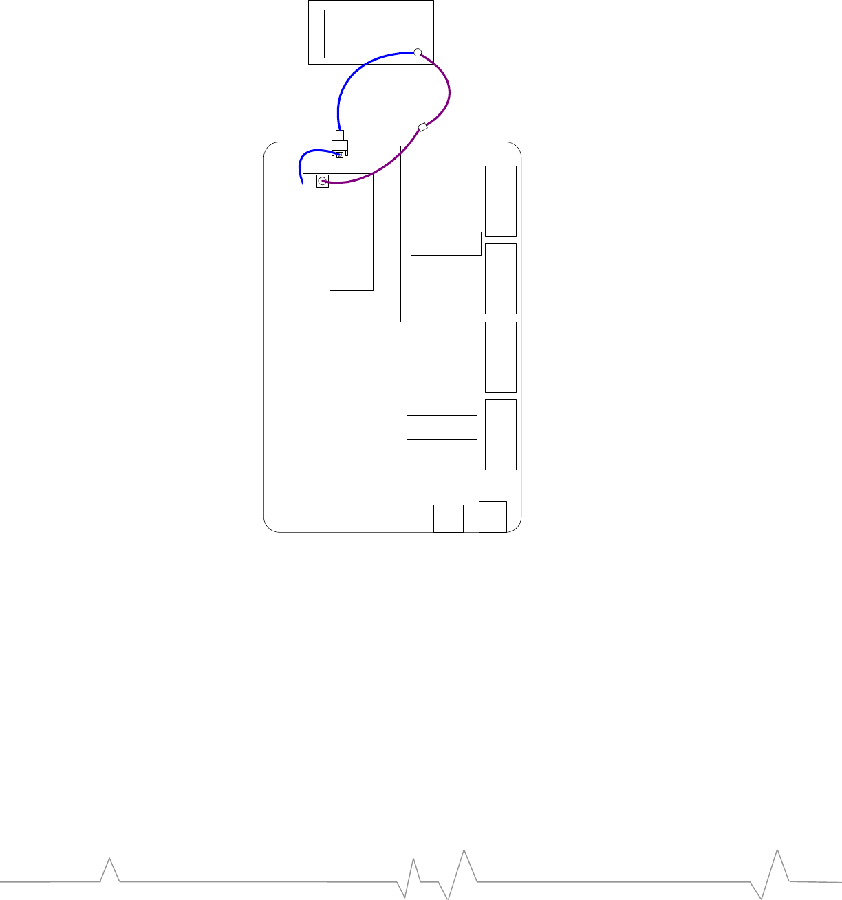
Boxed configuration
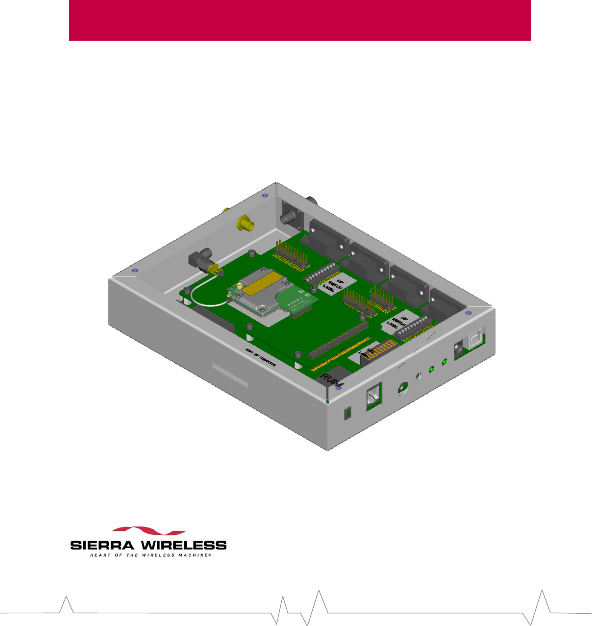
Theboxed(demo)configurationisshownbelow.Youmustspecifythisdelivery
optionatthetimeofordering.Notethatthisconfigurationisnotpreferablefor
developmentuse,sinceonlyasubsetoftheinterfacesisavailable.Itisintended
forinitialEMevaluationordemonstrationonly.
Thediagrambelowdepictsalloftheavailableinterfacesandindicatorsforthe
boxedconfiguration,andisshownwiththelidoffforclarity.Notethatthe
internalRFcableconnectseithertotheSMAortotheTNCbulkheadadapter,not
both.
PAGE 9
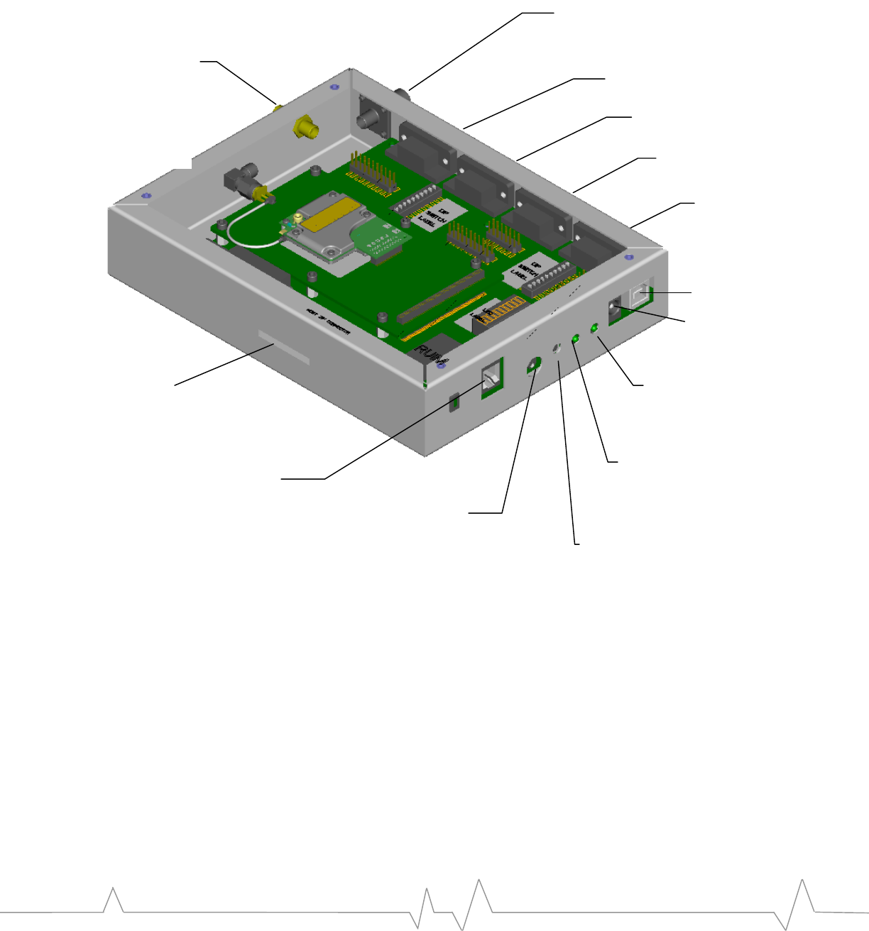
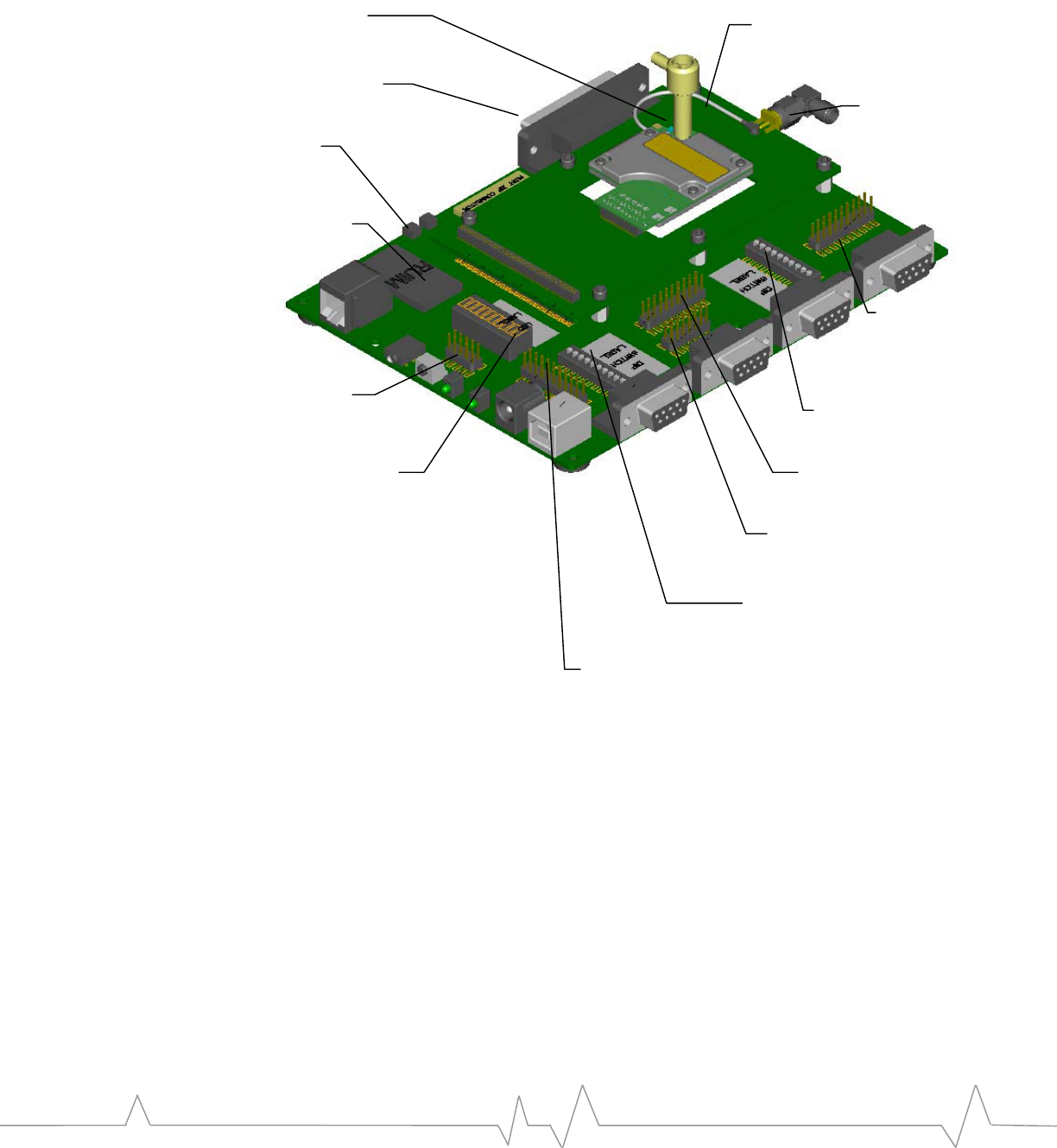
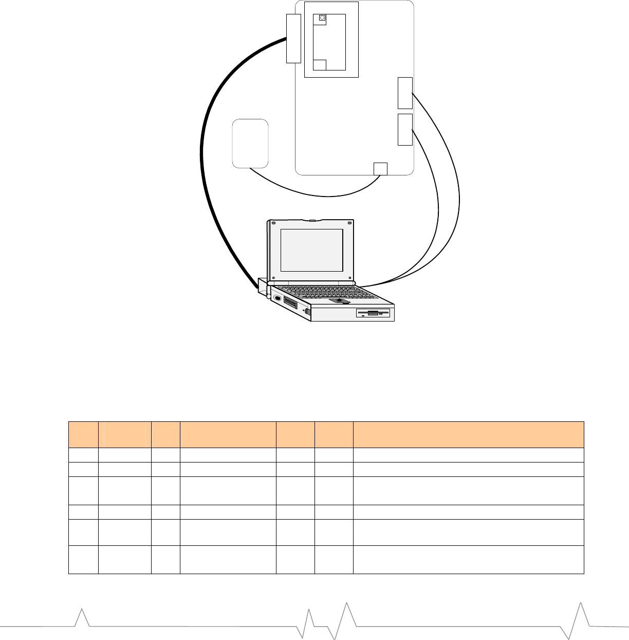
Figure1‐UDKboxedConfiguration
TxDn See UART monitor
support on page 24.
USB. See USB on
page .27.
UART1 See UART
signals on page 23.
UART2 See UART
signals on page 23.
UART3 See UART
signals on page 23.
TNC Adapter. (Typically not
installed) See 50Ω Connection on
page 38.
SMA Adapter.
See 50Ω Connection
on page 38.
UDK Power LED. See D11
–
Board power LED on
page 22.
Module Power LED. See D12 –
Module power LED on page
22.
Wall Cube Input. See
AC wall cube power
on page 13.
Reset Button. See Reset
switch on page 30.
Headset Jack. See Using a
headset on page 35.
Handset Jack. See Using a
handset on page 37.
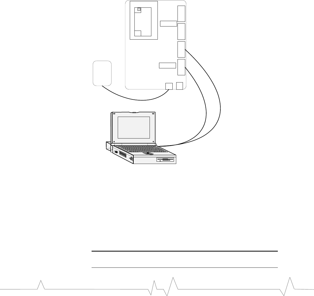
Bench configuration
Thebenchconfigurationisthemostcommon‐usedconfiguration.Thisisan
open‐boardconfigurationwithaccesstoalldevelopmentfeatures.TheEM3420
DaughterCardisshowninthediagramasanexample.
Theembeddedmodule’sRFadaptercanalsobeaccesseddirectlyinthis
configurationinordertominimizeRFlosses.Theseadditionalinterfacesare
showninFigure2‐UDKbenchconfiguration
PAGE 10
SETUP AND INSTALLATION
Figure2‐UDKbenchconfiguration
CEPC / Parallel Interface. See page 19.
EM RF Adapter. See page 38.
SMA Adapter.
See page 38.
EM3420 Daughter Card
RUIM Connector. See page 24.
Battery Header. See page 32.
MIO Header
See page 31.
Digital / Control DIP
Switch. See page 27.
UART Header. See
page 30.
MSM JTAG Header.
See
p
a
g
e 31.
Analog Header. See
p
a
g
e 31.
Analog / Control DIP
Switch. See page 29.
CPLD Program
Header. See
p
a
g
e 32.
10x DIP LED. See
page 21.
PAGE 11
Setup and Installation
Quick setup
Tosetupandinstallthedevelopmentkit:
1.ConfiguretheUDKDIPswitchesforStandaloneMode.SeeTypicalDIP
switchsettingsonpage29.Theboxedconfigurationhaspre‐configured
defaultsettings.
2.ConnecttheDevelopmentKittoaPC(orotherhost)viaserialcable(s).
3.PlugthewalloutletpowerbrickACcableintoanACreceptacle,thenplug
theDCcableintothedevelopmentkit.
4.ConnectthecablefromthedevelopmentkitSMARFconnectortothecall
boxorCDMAemulator;pleasecontactSierraWirelessApplications
Engineeringforadditionalsetupinformation.
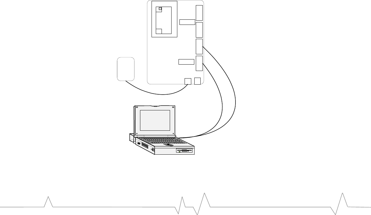
PC connections
ThedevelopmentkitmaybeconnectedtoaPCinadualUARTconfigurationor
USB+singleUARTasillustratedbelow.AUSB‐onlyconfigurationisnotshown.
Figure3‐DualUARTandUSB+UARTConfigurations
Universal Dev Kit
Daughter Card
UART 1
DC Input
Wall
Cube
UART 2
Serial Cable(s)
EM
USB
UART 3 TxDn
SW2
SW3
Data Control
PAGE 12
SETUP AND INSTALLATION
Universal Dev Kit
Daughter Card
UART 1
DC Input
Wall
Cube
UART 2
Serial Cable(s)
EM
USB
UART 3 TxDn
SW2
SW3
Data Control
Notethat“COMA”and“COMB”labelsareusedonthehostPCintheabove
diagram.ThisistoidentifythephysicalCOMportsandshouldnotbeconfused
withtheCOMportnumberassignedbyWindows.
Powering the Development Kit
Therearetwooptionsforpoweringthedevelopmentkit,usinganAC“wall‐
cube”orDCpowerfromanexternalpowersupply.
AC wall cube power
WhenusingtheAC“wall‐cube”,theDCoutputjackfromthewall‐cubeconnects
tothe“DCInput”jackonthedevelopmentkit,CN5.
Ifthe“wall‐cube”suppliedwiththeDevPlatformisnotsuitable,anotherwall‐
cubemaybeusedsolongasithasa5Voutputratedforatleast2Ampswiththe
jackbarrelexteriorgroundedand5Vonthebarrelinterior.
WhenusingtheUDKinthepackagedconfiguration,SwitchSW2‐1mustbein
theOFFposition,asthisisinparallelwiththebox‐mountedpowerswitch.
TurningSW2‐1ONover‐ridestheexternalswitch.Table3showstherequired
switchsettingswhenusingwall‐cubepower.
Table3‐Powerswitchsettings
SW2-1 External Power Switch Module Power State
OFF X OFF
Bench
Configuration ON X ON
OFF OFF OFF
OFF ON ON
Boxed
Configuration ON X ON
PAGE 13
Whenusingthewallcubeinput,thereare2settingsforbatteryvoltage.SW3‐8is
closedtosetthevoltagetoanominalvalue(~3.9V).Thisisthedefaultsetting,
andshouldbeusedinmostcases.Whenopen,thevoltagecanbeadjustedusing
R394fortestinglow‐orhigh‐batteryvoltageconditions.Adjustmentranges
between3.0V~4.5V,asshowninTable4.
ToadjusttheVBATTvoltage,measureatTP17&TP18andadjustR394.Note
thatSW3‐8mustbeOFFinordertoadjustVBATTvoltageaccordingtothetable.
Table4‐VBATTvoltageadjustment
SW3-8 R394 VBATT Voltage
ON X ~3.9V
OFF Full CCW ~3.0V
OFF Full CW ~4.5V
DC power
IfusingaDCpowersourcewithoutajackconnector,theDCvoltagemustbe
between3.6Vand4.2Vandratedforatleast2amps.TheDCvoltagemustbe
connectedtothedevelopmentkitonTP17(VBATT)andgroundmustbe
connectedonTP18.Inthisconfiguration,SW2‐1mustbeturnedOFF.
RF Connection
TheboxedconfigurationconnectstoaCDMAcallboxorotherRFtest
equipmentviatheexternalSMAconnector.Forthebenchconfiguration,there
aretwooptions.
1.UsetheSMAconnectorattheendofthedaughtercard.Thisprovidesthe
mostcommonlyavailableconnectortype,sonospecialRFadaptersare
required.
2.Directconnection.TheEM’sRFconnectorprovidesminimalRFlosses,but
requiresaspecialRFadapter.TheadaptertypedependsontheEMmodelis
suppliedwithyourUDK.
Bothconfigurationsareshownbelow,withOption1showninblueandOption2
inviolet.
PAGE 14

Development Kit Features
Introduction
Thedevelopmentkitincludesanumberofswitchesforvariouscontrolsand
configurationoptions.Thissectiondiscussestheseswitches,LEDindicatorsand
thevariousdevelopmentkitheadersandconnectors.
Modes of operation
Thedevelopmentkitsupportsfourmodesofoperation:standalonemode,host
developmentmode,extendermodeandCEPCmode.Inallmodesofoperation,
theembeddedmoduleismountedonthedevelopmentkitdaughtercard,which
isspecificallydesignedforagivenEMmodel.
• Standalonemodeallowsforoperationofthemoduleindependentofthe
targethostsystem.Theinterfaceprotocolisforcedto“DM”protocol,
allowingcommunicationwiththelowest‐leveldevelopmenttools.
• HostDevelopmentmodealsoallowsthemoduletooperate
independentlyofthetargethostsystem,howevertheprotocolis
compatiblewiththetargethostdevice.
• Extendermodeassistswithhardwareandsoftwareintegrationofthe
moduleintothetargethostsystem.
• CEPCmodeallowsaspeciallyconfiguredPCtocontrolhost‐modem
handshakingsignalsandpowercontrolduringearlystagesofWindows
CEdevelopment.
Eachmodeofoperationisrequiredtosatisfytheinterfacerequirementsofthe
EMmodelbeingused.See“EmbeddedModuleHardwareIntegrationGuide”for
detailsonhost‐modemhandshaking.ByenablingtheModuleWakeDIPSwitch
SW2‐6(seeSW2–DigitalcontrolDIPswitch),theUDKassertsthenecessary
signalstokeeptheEMcommunicatingwiththehostplatform.
PleaseseethetablesunderheadingSW2–DigitalcontrolDIPswitchforthe
typicalswitchsettingsforeachmode.
Standalone mode
Standalonemodeisintendedforproductevaluationandearlydevelopment
independentofthetargethostsystem.Instandalonemode,aPCorotherhost
cancommunicatewiththedevelopmentkitviaserialports.Usethesameserial
portconfigurationdescribedlaterinthisdocument.Standalonemodealso
supportsaudiotestcapabilityviaa2.5mmheadsetjackandRJ‐11handsetjack.
Tosetthedevelopmentkitforstandalonemode,SwitchesSW2.6andSW2.7
mustbeturnedONbeforeresettingthemodule(viaSW1).Itisrecommendedto
usethedefaultswitchsettingsasshownunderTypicalDIPswitchsettingson
page29.
PAGE 16
DEVELOPMENT KIT FEATURES
SettingSW2.6andSW2.7forStandalonemodeandresettingthemodule,forces
theserialinterfacetousethe“DM”protocolwhichiscompatiblewiththelow‐
leveldebugtools.ThisistrueformodulesusingeitherCnSorHIprotocols.
SeeFigure5foranexampleofstandaloneoperationfortheDualUART
configuration.
Figure5‐Standalonemodeconnectiondiagram
Universal Dev Kit
Daughter Card
UART 1
DC Input
Wall
Cube
UART 2
Serial Cable(s)
EM
USB
UART 3 TxDn
SW2
SW3
Data Port Control Port
Host Development mode
HostDevelopmentmodeisintendedforhostprotocoldevelopmentindependent
ofthetargethostsystem.InHostDevelopmentmode,aPCorotherhostcan
communicatewiththedevelopmentkitviaserialports.Usethesameserialport
configurationdescribedlaterinthisdocument.HostDevelopmentmodealso
supportsaudiotestcapabilityviaa2.5mmheadsetjackandRJ‐11handsetjack.
TosetthedevelopmentkitforHostDevelopmentmode,SwitchesSW2.7mustbe
turnedOFFbeforeresettingthemodule(viaSW1).
IMPORTANT!SwitchSW2.6canbeturnedeitherONorOFFduringreset,butmust
beturnedOFFforthemoduletofullypowerdownatanytime!
PAGE 17
TheconnectiondiagramisthesameasthatshownforStandaloneMode.The
tablebelowshowstheeffectofswitchesSW2‐6andSW2‐7followingamodule
reset.Thestatesshowninthistablearevalidonlywhenhandshakingisenabled.
Table5–Standalone/HostDevelopmentmodeswitchconfigurations
Operating Mode SW2-6
Module Wake
SW2-7
Host Status
Behavior
Standalone Mode ON ON DM Protocol; communication
channel never closes
Host Development Mode ON / OFF OFF CnS or HI Protocol; communication
channel follows the state of
MODULE_WAKE
Extender Mode
Inextendermode,ablank“EMPod”isinstalledinthetargethostinplaceofthe
EM.This“dummy”moduleprovidesaflexcableconnectiontothedevelopment
kit,butnoEMcircuitry.Inthisarrangement,theEMonthedevelopmentkitis
poweredandcontrolledbythetargethost.Thismodeofoperationallowsfor
probinganumberofthesignalsonthemodulehostinterfaceconnector.
AdditionallytheserialportscanbeconfiguredtoallowmonitoringofRXandTX
communicationdirectionsforbothportsusingaserialportanalyzer.
Twocontrolswitchchanges(fromstandalone/hostdevelopmentmodes)are
requiredtosupportextendermode.Thedevelopmentkitmainboardwillrelease
therequiredcontrol/handshakingsignalswhentheflexcableisdetected,
dependingonthepositionoftheModuleWake&HostStatusswitches.Analog
switchesrequiringsetupareforbatteryconnectionandmonitoring.These
optionsareshowninthefollowingtable:
Table6‐Extendermodeswitchconfiguration
Switch
Position Signal OFF ON
SW2-6 MODULE_WAKE Tri-states Module Wake signal to the
EM, allowing these to be controlled by
the Host.
Drives Module Wake signal
to the EM, forcing control
channel ON
SW2-7 HOST_STATUS Tri-states Host Status signal to the
EM, allowing these to be controlled by
the Host.
Drives Host Status signal to
the EM, forcing control
channel ON
SW3-9 AUXV0 ↔ VBATT Isolates AUXV0 pin on EM connector Connects VBATT to AUXV0
pin on EM connector
SW3-10 VBATT ↔
HOST_VBATT Isolates dev kit VBATT from Host
battery voltage Supplies dev kit VBATT
from host battery voltage
AdiagramshowingExtendermodeinterconnectionisshownbelow.This
exampleshowsadual‐UARTconfiguration.Extendermodeinitsmostbasic
formsimplyroutessignalsbetweenthehostandEMviaaCPLD.
NotethatTxDalwaysoriginatesfromtheHost(DTE),andRxDoriginatesfrom
theEM(DCE).Signaldirectionsareindicatedinthediagram.
PAGE 18
DEVELOPMENT KIT FEATURES
CertainEMmodelsbringoneormoreAuxiliaryAnalog‐to‐digitalinputs
numbered(0...)outtothehostconnector.AUXV0isreservedformeasuring
batteryvoltage,andAUXV1,AUXV2,etc.canbeconnectedforgeneraluse.
SupportedAUXVnsignalpinsaredefinedintheEMReferenceGuides.
Figure6‐Extendermodeconfiguration
Universal Dev Kit
Daughter Card
UART 1
DC Input
Wall
Cube
UART 2
EM
TxD 1TxD 2
CPLD
EM
Pod
Host
Platform
TxD1RxD1
TxD2RxD2
RxD1
TxD1
RxD2TxD2
CEPC mode
CEPCisaspeciallyconfiguredPC,runningWindowsCEonPCplatform
(CEPC).ThePC’sparallelportdirectlyinterfacestotheUniversalDevKitto
performpowercontrolandsignalingfunctions.Signalsusedforthisinterface
conformtotheHost‐ModemHandshakingSpecificationRev3.7.
SimilartoExtenderMode,theUDKmainboardwillreleasetherequired
control/handshakingsignalswhentheparallelcableisdetected,dependingon
thepositionoftheModuleWakeandHostStatusswitches(refertothetable
below).
Table7‐CEPCswitchsettings
Switch
position Signal OFF ON
SW2-6 MODULE_
WAKE Tri-states Module Wake signal to the EM,
allowing these to be controlled by the Host. Drives Module Wake signal to the
EM, forcing control channel ON
SW2-7 HOST_ST
ATUS Tri-states Host Status signal to the EM,
allowing these to be controlled by the Host. Drives Host Status signal to the
EM, forcing control channel ON.
PAGE 19
ThefollowingdiagramshowsinterconnectionbetweenthePCandEM
DevelopmentBoard,usingastandardDB‐25parallelcableand2serialcables.
Figure7–CEPCconnectiondiagram
Universal Dev Kit
Daughter Card
UART 1
DC Input
Wall
Cube
UART 2
(2) Serial Cables
EM
DB-25
Data Port Control Port
CEPC
(WinCE
Emulator)
ThefollowingtableshowspinoutandsignalnamesforthePCparallelportand
UDK,signaldirectionandsignaldescription.TheActivecolumndefinesthe
activestateforthePCparallelportonly.TheUDKthentranslatesthesesignals
accordingtoEMtypedetected.
Table8‐CEPCSignalDefinition
PC
pin PC
signal Dir UDK Signal UDK
pin
Active Description
2 Data 0
Æ ON/OFF_EM 27 High High level turns the EM on
3 Data 1
Æ RESET_N 25 Low Low pulse resets the EM
4 Data 2
Æ MODULE_WAKE 30 High High level tells EM to wake up;
Enable the control channel
5 Data 3
Æ HOST_STATUS 28 High Low level tells EM to keep control channel open
12 +Paper
End
Å HOST_WAKE 29 High High level tells the host that the EM has high
priority message to send
13 +Select Å MODEM_
STATUS
26 Low Low level tells host that EM has been reset;
High level: control channel has been initialized
PAGE 20
DEVELOPMENT KIT FEATURES
TwoCEPCfunctionsaretypicallydevelopedindependently–powercontroland
host‐modemhandshaking.TheModuleWakeswitch(SW2‐6)shouldbeturned
ONwhileHost‐ModemHandshakingisnotbeingcontrolledbytheCEPC.This
willallowproperdebugofthePowerControlfunction.
LED Indicators
D10 – 10-segment LED
TheUniversalDevelopmentKitsupportsa10‐segmentLEDbartodisplay
digitalsignalstatus,plus2power/statusindicators.
Eachsegmentofthe10‐segmentdisplayisrelatedtoanIOsignalasshowninthe
tablebelow.TheLEDlightsupwhenthesignalisintheACTIVEstate;andoff
whenthesignalisintheINACTIVEstate.
TwomapsareavailableforagivenEMmodel.TheprimaryLEDmapisenabled
bydefault,andisusedforhost‐modemhandshakingsignalstatesandselected
UART1andUART2signals.TheprimaryLEDmapformostembeddedmodules
isshownbelow:
Table9‐Primary10‐segmentLEDmap
D13 10-Segment LED Array (Primary map)
Pos Label Name Description
1 Module Wake MODULE_WAKE - wakeup signal from host
2 Host Status HOST_STATUS - status signal from host
3 Host Wake HOST_WAKE - wakeup signal from EM
4 Modem Reset MODEM_RESET_STATUS - from EM
5 DTR1/ UART1 Data Terminal Ready - from host
6 DSR1/ UART1 Data Set Ready - from EM
7 CD1/ UART1 Carrier Detect - from EM
8 RI1/ UART1 Ring Indicator - from EM
9 TXD2 UART2 Transmit Data - from host
10 RXD2 UART2 Receive Data - from EM
SomeEMmodelsalsosupportfullUART1signalstatususingaDIPswitchon
theirDaughterCard.ThisplacesTxD1,RTS1/,RxD1,andCTS1/ontoPositions
1~4,respectively.Positions5~10remainpertheabovetable.Refertothe
ReferenceGuideforyourEMmodelformoredetails.
ThesecondaryLEDmapformostembeddedmodulessupportsXIM
development.TousethisLEDmap,MIO19mustbepulledhigh(seeCN12.3
detailsinCN12‐MIO(ModuleInput/Output)signaltestpointsonpage31).
NotethatagivenEMmodelsupportsonlyoneXIMinterface,theotherwill
defaulttoaUARTinterface.ForexampleEM3420usesUART3fortheRUIM
interface,sointheLEDmapbelow,UART2signalswillapplytopositions7~10.
PAGE 21
Table10‐Secondary10‐segmentLEDmap
D13 10-Segment LED Array (Secondary map)
Pos Label Name Description
1 XIM_EN3 TXD3 pin, enables XIM VCC when high
2 XIM_IO3 RXD3 pin, bidirectional XIM data
3 XIM_RST3 RTS3_N pin, active high reset to XIM card
4 XIM_CLK3 CTS3_N pin, XIM clock
5 XIM_DET GPIO5 PD, goes high when card is inserted
6 N.U. Not Used
7 XIM_EN2 TXD2 pin, enables XIM VCC when high
8 XIM_RST2 RTS2_N pin, active high reset to XIM card
9 XIM_CLK2 CTS2_N pin, XIM clock
10 XIM_IO2 RXD2 pin, bidirectional XIM data
OthercombinationsofLEDsignalingcanbeassignedforspecificdevelopment
tasksorEMinterfacecapabilitiesviaCPLD,asrequired.Theseassignmentsmay
varybetweenEMmodels;seetheReferenceGuideforyourspecificmodule.
NOTE:The10segmentLEDisalsousedtodisplaytheCPLDcodeversion,whenthe
daughtercardisremoved.TheLEDEnableswitchmustbeturnedOFFtoviewthiscode.
Thecodeversionisdisplayedasabinarynumber,withLEDD13.1beingtheLSB.
D11 – Board power LED
D11istheBoardPowerindicator,anddisplaysGREENwhentheUDKmain
boardispoweredon.
D12 – Module power LED
D12istheModulePowerindicator,whichdisplaysGREENorREDwhenthe
Moduleispoweredon.TheLEDisturnedOFFwhentheModulepowercontrol
isOFF(viatheUDK).Thiscombinationofindicationisvalidforstandalone
mode,ExtenderModeorCEPC,accordingtothetablebelow.
Table11‐D12powerLEDstates
D12 State Description
OFF Power control to the EM is in the OFF state. Controlled by
SW2-1 unless in Extender Mode or using CEPC.
GREEN The EM is ON, and reset is inactive
RED The EM is turned ON, but either power is not detected or the
EM is in the reset state.
PAGE 22
DEVELOPMENT KIT FEATURES
Serial Interfaces
UART (1~3) - DE9
UsedtoaccesstheEMUARTs,RS‐232compatibleupto8‐wireinterface
(UART1),2‐or4‐wireinterface(UART2&UART3).RTS/CTSfunctionalityis
optionalforUART2&UART3.UART1containsallflowcontrolsignals,andis
usedprimarilyasthedataport(i.e.ATcommandinterface)forUART‐only
implementations.
ItmaybenecessarytoadjusttheEMdataportUARTduringdevelopment,as
thedefaultdatarateis230kbps.MostPC’sdonotsupportmorethan115kbps
withoutaspecializedserialportadapter(availableasSierraWirelessaccessory).
ScriptsareprovidedontheCD‐ROMtoconfigureUART1for115kbpsor230
kbps.
UART signals
SignalsfromthemoduleconnectortothisDE9willbelevelshiftedusinganRS‐
232transceiver.
Table12‐UARTsignals
Pin # UART1
Signal Name
UART2
Signal Name
UART3
Signal Name
TxDn
Signal Name
1 CD1_N NC NC NC
2 RXD1 RXD2 RXD3 NC
3 TXD1 TXD2 TXD3 TXDn
4 DTR1_N NC NC NC
5 GND GND GND GND
6 DSR1_N NC NC NC
7 RTS1_N RTS2_N RTS3_N NC
8 CTS1_N CTS2_N CTS3_N NC
9 RI1_N NC NC NC
Ref.
Des. CN2 CN1 CN13 CN14
UART switches
EachUARTcanbeindividuallyselectedusingSW2positions3~5,wherethe
switchONposition=UARTnSelected.NotethattheEmbeddedModule
FirmwaresettingdeterminestheUARTselection.TheUDKUARTselectionsare
shownbelow.
Table13‐UARTSwitchSettings
Switch Position Select UARTn
SW2-3 UART1
SW2-4 UART2
SW2-5 UART3
PAGE 23
UART monitor support
The4DE9connectorsaredynamicallyassigned,basedonthecombinationof
DIPswitchsettingsforSW2‐3,‐4and‐5.Thefollowingtableshowsthese
assignments.FortheExtenderModecase,thefullUARTuseisturnedoff,
howevertheRxDsignalwillstillbetransmittedtotheconnectorperthetable.
See*notebelowthetableformoredetails.
Table14‐UARTMonitorConnections
SW2-5
(UART3)
SW2-4
(UART2)
SW2-3
(UART1)
CN2
(UART1)
CN1
(UART2)
CN13
(UART3)
CN14
(TxDn)
0 0 0 - - - -
0 0 1 UART1 - - TxD1
0 1 0 - UART2 TxD2 TxD2
0 1 1 UART1 UART2 TxD2 TxD1
1 0 0 - TxD3 UART3 -
1 0 1 UART1 TxD3 UART3 TxD1
1 1 0 - UART2 UART3 TxD2
UART Switch Setting
1 1 1
UART Signal Assignment
UART1 UART2 UART3 TxD1
*Note:Forextendermode,RxDnreplacesUARTnintheaboveassignmenttable.
ThismeansthatonlytheRxDsignalispassedoutthroughtheseconnectors
whenusingextendermode.Signalsinbothdirectionscanbemonitored,but
fromdifferentconnectors.
SignalTxDnisprovidedonthefourthDE9connector.Thissignalisused
exclusivelyformonitormode.TxDnassignmentisdefinedinTable14above.
Notethatformonitormode,amaximumof4signalscanbemonitoredinadual‐
UARTconfiguration:
• TxD1,RxD1,TxD2,RxD2aremonitoredwhenusingUART1+UART2
• TxD1,RxD1,TxD3,RxD3aremonitoredwhenusingUART1+UART3
• UART2+UART3isconfigurableonthedevelopmentkit,butistypicallynot
usedinanyEM.
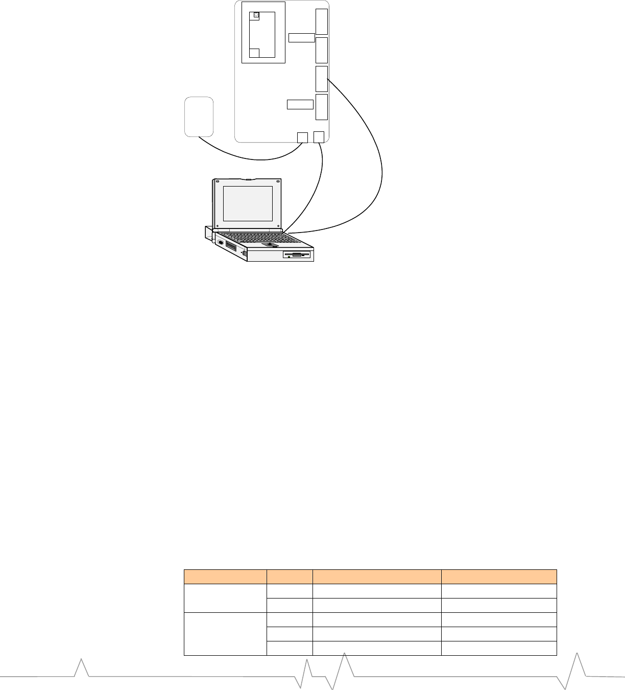
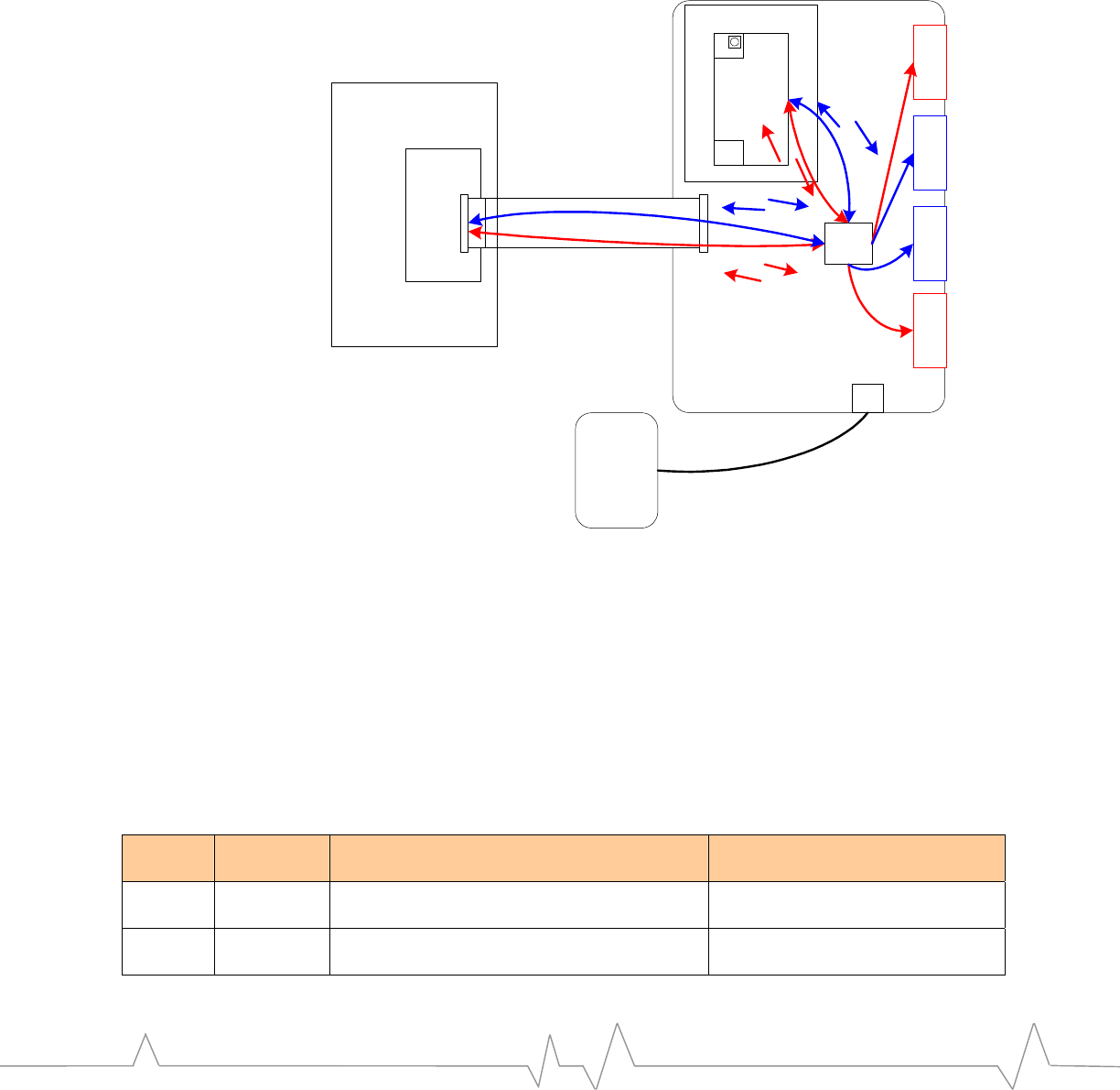
TheinterconnectformonitormodeoperationisshowninFigure8.Here,the
UDKisusedintheextendermode(seepage17),tomonitorUART1and/or
UART2.Inthisconfiguration,theSW2settingsfromTable14areSW2‐5,4,3=0,
1,1inordertoenableUART1andUART2.
InFigure8theUART2connectormonitorsRxD2(signalsfromEMÆhost),and
TxD2monitorssignalsfromthehostÆEM.
ItisalsopossibletomonitorbothdirectionsofUART1inthisconfiguration,
wheretheUART1connectormonitorsRxD1(signalsfromEMÆhost),andTxD1
monitorssignalsfromthehostÆEM.
PAGE 24
DEVELOPMENT KIT FEATURES
Figure8‐Monitormodeconnectionexample
Universal Dev Kit
Daughter Card
UART 1
DC Input
Wall
Cube
UART 2
EM
TxD 1
TxD 2
CPLD
TxD2
Protocol Analyzer
Monitors TxD & RxD pins
**Requires adapter cable
EM
Pod
Host
Platform
RxD2
TxD1RxD1
TxD2RxD2
RxD1
TxD1
RxD2TxD2
PC used as "sniffer"
Monitors RxD pin of COMx
RxD2
TxD2
**See adapter
cable schematic
AY‐adaptercableisusedtomonitorbothTxDandRxDusingaprotocol
analyzer.ThisputsRxDontopin2andTxDontopin3oftheprotocolanalyzer’s
DE9plug.Theschematicforthiscableisshownbelow.
PAGE 25
Figure9‐ProtocolanalyzerY‐adaptercable
1 5
6 9
1 5
6 9
1 5
6 9
DE9 PLUGDE9 PLUG
DE9 SOCKET
Ground
TxD
Ground
RxD
To Protocol
Analyzer
TxD
From Host
RxD
From EM
XIM interface
SomeembeddedmodulescansupportXIMoneitherUART2orUART3.When
theEMfirmwareisconfiguredforXIM,theassociatedUARTfunctionisnot
available.
DIPswitchsettingsareusedtoenableXIM.SelectXIMforUART2orUART3
pinoutsaccordingtothetablebelow.NotethattheXIMselection,whenenabled,
overridesTable13fortheselectedUART.Forexample,ifUART2isenabledin
Table13andXIMisenabledwithUART2selectedinTable15,thenTable13
behavesasifUART2isNOTselected.
Table15‐XIMswitchsettings
SW2-10
setting SW2-9
setting XIM configuration
OFF X XIM disabled
ON OFF XIM enabled on UART2
ON ON XIM enabled on UART3
NotethatthedetectionofanXIMcardisconfigurable,andshouldbedetermined
duringthedesignoftheHost/EMinterface.Typically,anavailableMIOisused
inalevel‐triggeredinterruptorpolledmode.Anyrequireddetectioncircuitryis
afunctionoftheHostboarddesign.
AsshowninTable16thedetectionmechanismfortheUDKisacontactthat
closesbetweenpins4&8whentheXIMcardisinsertedwiththeCN25latch
connectorclosed.TheXIM_DET_POLsignalisthedetectionpolarity,whichis
setontheEMdaughtercard.IftheMIOusedforXIM_DETcontainsapull‐down
element,thenthesignalXIM_DET_POLwouldbetiedhigh,andvice‐versa.
PAGE 26
DEVELOPMENT KIT FEATURES
Table16‐CN25XIMsignalinterface
Pin # Signal name Direction Description
1 VCC_XIM To Card VCC supply for XIM card
2 XIM_RST To Card Active HI reset signal
3 XIM_CLK To Card Clock signal
4 XIM_DET_POL To Socket Detection polarity (UDK only)
5 GROUND Ground
6 XIM_VPP N/A Not Used
7 XIM_IO Bidirectional Data to/from XIM card
8 XIM_DET From Socket XIM detect to MSM
USB
PerformsdirectconnectiontoaPCformodulesthatsupportUSB.Noadditional
signalsorswitchesarerequired,howevertheEMand/ordaughtercardmustbe
configuredwithaUSBtransceiverandthenecessaryfirmware.
Table17‐USBsignalinterface
CN20 Pin # Signal name
1 VCC_USB
2 USB-
3 USB+
4 Ground
WhenusingamodulewiththeUSBinterface,itmaynotbepossibletouse
certaininterfacecombinations.Forexample,theMSM6050’sUART3pins
interfacewiththeUSBtransceiver,soUART3cannotbeused.Inthiscase,SW2‐5
UART3mustbeintheOFFpositiontoavoidcontention.SeetheReference
GuideforyourEmbeddedModulefordetailsonwhichinterfacecombinations
arenotpossible.
TheUDKusesMIO(1)andMIO(2)toroutethesignalsUSB+andUSB‐,
respectively.TheseMIOsignalsarenotavailableforgeneraluseinthiscase.
Switches
SW2 – Digital control DIP switch
DIPswitchSW2isusedfordigitalcontrolfunctions.Certainfunctionsareover‐
riddeninExtenderModeand/orCEPCMode,meaningthatconnectionofa
CEPCorExtendercableareautomaticallydetected,sotheswitchsettingdoes
notneedtobechanged.Thesefunctionsareindicatedinthetablebelow,inthe
farrightcolumns.
PAGE 27

Table18‐Switch2(SW2)settings
Switch
position Function Extender
override CEPC
override
1 MODULE_ON– This switch is used to turn the module on. Turning the
switch to OFF position turns modem OFF. Turning switch to ON
position turns modem ON. This switch is only used in standalone mode
to control modem power state. In the extender and CEPC modes this
switch position is overridden in the CPLD.
√ √
2 Battery Enable – Enables the barrel jack LDO regulator / Battery supply,
which powers up the Universal Dev Kit board. Turn this switch ON to
use the wall cube input to supply the EM. Turn this switch OFF if using
DC Power at the battery terminals.
3 UART1 Select – Turn this switch ON to enable UART1
communications. This enables both the RS-232 transmitter and receiver
for UART1. This switch setting is ignored when using Extender Mode,
where only monitoring of RS-232 signals is possible.
√
4 UART2 Select – Turn this switch ON to enable UART2
communications.
√
5 UART3 Select – Turn this switch ON to enable UART3
communications. Note that UART3 must be disabled when using the
USB interface with the MSM6050. See the Reference Guide for the
associated EM for details.
√
6 Module Wake – Turn this switch ON to activate the MODULE_WAKE
signal. Used in conjunction with SW2.7 Host Status during reset to
initiate Standalone Mode.
7 Host Status – Turn this switch ON to activate the HOST_STATUS
signal. Used in conjunction with SW2.6 Module Wake during reset to
initiate Standalone Mode.
8 LED Enable – Enables the MIO LED array. Turn this switch ON to
enable the LED array.
9 XIM Select – This switch selects which MSM UART channel will be
used for XIM mode, only when XIM is enabled by SW2-10. Turn this
switch OFF (Low) to select UART2, and ON (High) to select UART3.
10 XIM Enable – Turn this switch ON to enable XIM on UART2 or UART3
(as per SW2-9 setting). The combination of XIM enable and XIM select
will override the UARTn Select function switch for SW2-4 and SW2-5
above. That is, the XIM selection takes precedence over the UART
function.
See XIM interface on page 26 for more details.
PAGE 28
DEVELOPMENT KIT FEATURES
SW3 – Analog DIP switch
Table19‐Switch3(SW3)Settings
See the section below for Typical DIP switch settings, and specific Embedded Module
Reference Guides for alternate DIP switch setting scenarios.
Typical DIP switch settings
TypicalDIPswitchsettingsfordualUARTuseareshownbelowforthe
standalone,hostdevelopment,extender,andCEPCmodesofoperation.These
settingsareastartingpointonly,andnotnecessarilythepreferredcombinations.
SeetotheReferenceGuideforyourEMmodelnumberformoreoptions.
Table20‐SW2typicalsettings
SW2 Digital Control DIP Switch – Dual UART Typical Settings
Pos Label Name Description Standalone Host Dev. Extender CEPC
1 Module ON Turn Embedded Module ON ON X X
2 Battery Enable Enable barrel jack LDO ON ON ON
3 UART1 Select Select UART1 ON X ON
4 UART2 Select Select UART2 ON X ON
5 UART3 Select Select UART3 OFF OFF OFF
6 Module Wake Activates Module Wake ON (& reset) ON ON / OFF ON / OFF
7 Host Status Activates Host Status ON (& reset) OFF ON / OFF ON / OFF
8 LED Enable Enables MIO LED array ON ON ON
9 XIM Select XIM Select:
OFF=UART2 / ON=UART3
ON / OFF ON / OFF ON / OFF ON / OFF
10 XIM Enable Enables XIM on
UART2 or UART3
ON ON ON ON
Switch
position Function
1 MIC BIAS Control – This switch is used to enable an onboard mic bias for the headset. Turn to ON
position to enable bias at headset microphone. Turn to OFF position to disable bias. Turn to OFF
during extender mode.
2 MIC1P<Headset – When ON, connects MIC1P to the headset MIC pin.
3 MIC1N<Ground - When ON, connects MIC1N to Ground. Required when using the differential
MIC1 interface with a (single-ended) headset.
4 MIC2P<Headset – When ON, connects MIC2P to the headset MIC pin.
5 MIC2N<Ground - When ON, connects MIC2N to ground. Required when using the differential
MIC1 interface with a (single-ended) headset.
6 SPK1>Headset - When ON, connects SPK1P to the headset SPK pin.
7 SPK2>Headset - When ON, connects SPK2 to the headset SPK pin.
8 Bat Voltage Set – Sets the battery LDO regulator output to nominal voltage ~3.9V when turned ON.
When this switch is turned OFF, the LDO output voltage can be adjusted between 3.0~4.5V using
potentiometer R394.
9 AUXV0<Battery – When ON, connects the main battery voltage (VBATT) to the AUXV0 pin. This
ADC input is often used by the module to measure battery voltage. See the Reference Guide for
the EM model used.
10 Host<Battery - When ON, connects the main battery voltage (VBATT) to the Host battery voltage
(HOST_VBATT). Turn this switch OFF to isolate the HOST_BATTERY from the UDK VBATT net.
PAGE 29
Table21‐SW3TypicalSettings
SW3 Analog Control DIP Switch - Dual UART Typical Settings
Pos Label Name Description Standalone Extender CEPC
1 MIC Bias Enable Enable MIC Bias to headset jack ON ON ON
2 MIC1P<Headset Connect MIC1P to headset jack ON ON ON
3 MIC1N<Ground Connect MIC1N to (AC) ground ON ON ON
4 MIC2P<Headset Connect MIC2P to headset jack OFF OFF OFF EM3420 does not
5 MIC2N<Ground Connect MIC2N to (AC) ground OFF OFF OFF support MIC2/SPK2
6 SPK1P>Headset Connect SPK1P to headset jack ON ON ON
7 SPK2>Headset Connect SPK2 to headset jack OFF OFF OFF
8 Batt Voltage Set Set battery voltage LDO to
mid-level (~3.9V)
ON ON ON
9 AUXV0<Battery Connect AUXV0 to VBATT X X X
10 Host>Battery Connect VBATT to the host
battery pin
X ON / OFF X Depends on power
source
Reset switch
MomentaryswitchSW1resetstheEMwhenpressed.
Debug headers and connectors
Internaltothedevelopmentkitaretwostandard2‐row0.1”x0.1”headersthat
canbeusedforconnectinglogicanalyzerorscopeprobes.Athirdheaderisused
forprobinganalogsignals.
CN11 – UART signal test points
Table22‐CN11‐UARTsignaltestpoints
Signal name Pin # Pin # Signal name
1 2
3 4 CD1_N
RXD1 5 6 TXD1
DTR1_N 7 8 DSR1_N
RTS1_N 9 10 CTS1_N
RI1_N 11 12 TXD2
RXD2 13 14 CTS2_N
RTS2_N 15 16 TXD3
RXD3 17 18 CTS3_N
RTS3_N 19 20 GND
PAGE 30
DEVELOPMENT KIT FEATURES
CN12 - MIO (Module Input/Output) signal test points
Table23‐CN12‐MIOsignaltestpoints
Signal name Pin # Pin # Signal name
RESET_EM 1 2
MIO(19) 3 4 MIO(0)
MIO(1) 5 6 MIO(2)
MIO(3) 7 8 MIO(4)
MIO(5) 9 10 MIO(6)
MIO(7) 11 12 MIO(8)
MIO(9) 13 14 MIO(10)
MIO(11) 15 16 MIO(12)
MIO(13) 17 18 MIO(14)
MIO(15) 19 20 GND
CN3 - Analog test points
InadditiontotheAnalogtestheader,youcaninstallasetoftestclipstoassistin
connectingaudiotestequipment.Groundtestclipsareblackandsignaltestclips
arered.Thesetestclipsaredefinedinthetablebelow.RefertotheEmbedded
ModuleHardwareIntegrationGuideforinformationonusingtheaudiocircuitry.
Table24‐CN3‐analogtestpoints
Test clip Signal name Pin # Pin # Signal name
TP13 GND 1 2 GND
TP8 MIC1P 3 4 N.C.
TP7 MIC1N 5 6 VCC_MSM_P
TP11 MIC2P 7 8 VCC_BRD
TP9 MIC2N 9 10 VCC_XIM
TP5 SPK1P 11 12 VCC_USB
TP6 SPK1N 13 14 VCC_5V
TP10 SPK2 15 16 VBATT
TP12 RINGER/SPK3 17 18 AUXV0
TP14 GND 19 20 GND
CN15 – JTAG header
TheJTAGheadercanbeusedasanalternatemethodforprogrammingtheEM’s
FlashmemoryusingtheJTAGinterfacetotheMSMprocessor.Theheaderpins
outdirectlytotheLauterbachTrace32debugger.
Table25‐CN15‐JTAGheader
Signal name Pin # Pin # Signal name
VCC_MSM_P 1 2 GND
TRST_N 3 4 GND
TDI 5 6 GND
TMS 7 8 GND
PAGE 31
Signal name Pin # Pin # Signal name
TCK 9 10 GND
TDO 11 12 RESET_EM
VCC_MSM_P 13 14 GND
CN23 – ISR header
TheISR(In‐SystemReprogramming)headerisusedtoprogramtheCPLDson
theUniversalDevelopmentKit,whichisperformedbySierraWireless.Thethree
devicesaredaisy‐chainedtouseonlyoneheader.Noteyoumustremovethe
daughtercardtoprogramtheCPLDs.
Table26‐CN23‐ISRHeader
Signal name Pin # Pin # Signal name
GND 1 2 TMS
JTAG_EN 3 4 TCK
5 6 TDI
VCC_BRD 7 8
TDO 9 10 GND
J4 – Battery connector
J4canbeusedtodirectlyconnectabatteryfortestingchargeorlow‐battery
conditionbehavior.
Table27–J4Batteryconnectorpinout
J4 Pin # Signal name
1 VBATT
2 Ground
J5 – External power switch connector
J5routestheMODULE_ONsignaltotheexternalpowerswitch.Thisisused
onlyfortheboxedconfiguration.
Table28–J5Externalpowerswitchpinout
J4 Pin # Signal name
1 ON_SWITCH
2 MODULE_ON
CN27 - Board-to-board connector
A100‐pinboard‐to‐boardconnectoristheinterfacebetweentheUDKmain
boardandtheEMdaughtercard.ThereferenceguideforeachEMmodelshows
the100‐pinconnectorgroupedbyEMfunction.Table29
containsa100‐pinpinouttableindexedbytheUDKconnectorpinnumber.
PAGE 32
DEVELOPMENT KIT FEATURES
Table29‐UDK100‐pinConnectorPinoutbyEM3420Function
Pin # Signal Name Type Dir(1) Description
1
2
3
4
5
6
VBATT Power Bi-Dir Battery Voltage (3.7V Nominal)
7 SPK1P Audio IN Speaker 1 +
8 GND Power Bi-Dir Ground
9 MIC2P Audio OUT Microphone 2 +
10 GND Power Bi-Dir Ground
11 SPK1N Audio IN Speaker 1 -
12 GND Power Bi-Dir Ground
13 MIC2N Audio OUT Microphone 2 -
14 GND Power Bi-Dir Ground
15 SPK2 Audio IN Speaker 2
16 GND Power Bi-Dir Ground
17 MIC1P Audio OUT Microphone 1 +
18 GND Power Bi-Dir Ground
19 MIC1N Audio OUT Microphone 1 -
20 GND Power Bi-Dir Ground
21 VCC_USB Power OUT USB Transceiver Voltage
22 VCC_BRD Power OUT UDK Main Board Regulated Voltage
23 AUXV0 Analog OUT Battery Voltage tap for EM ADC
24 TP36 N/A N/A Test Point, not used
25 VCC_MSM_P Power IN MSM Digital Voltage from EM
26 VCC_XIM Power OUT XIM Card Digital Voltage
27 ON/OFF_EM Digital OUT On / Off control to EM
28 TP35 N/A N/A Test Point, not used
29 RESET_EM Digital OUT Reset control to EM
30 VCC_5V Power OUT UDK Main Board 5V from wall cube
31 MIO(8) Digital Bi-Dir Module Input/Output 8
32 TRST_N Digital OUT JTAG Test Reset
33 TXD2 Digital OUT Transmit Data UART2
34 TXD3 Digital OUT Transmit Data UART3
35 MIO(9) Digital Bi-Dir Module Input/Output 9
36 TDI Digital OUT JTAG Test Data Input
37 RXD2 Digital IN Receive Data UART2
38 RXD3 Digital IN Receive Data UART3
39 MIO(12) Digital Bi-Dir Module Input/Output 12
40 TMS Digital OUT JTAG Test Mode Set
41 CTS2_N Digital IN Clear to Send UART2
42 CTS3_N Digital IN Clear to Send UART3
PAGE 33

Pin # Signal Name Type Dir(1) Description
43 MIO(13) Digital Bi-Dir Module Input/Output 13
44 TCK Digital OUT JTAG Test Clock
45 RTS2_N Digital OUT Ready to Send UART2
46 RTS3_N Digital OUT Ready to Send UART2
47 MIO(14) Digital Bi-Dir Module Input/Output 14
48 TDO Digital IN JTAG Test Data Output
49 MIO(15) Digital Bi-Dir Module Input/Output 14
50 MODULE_WAKE Digital OUT Module Wake Handshaking signal
51 MIO(6) Digital Bi-Dir Module Input/Output 6
52 HOST_STATUS Digital OUT Host Status Handshaking signal
53 MIO(10) Digital Bi-Dir Module Input/Output 10
54 HOST_WAKE Digital IN Host Wake Handshaking signal
55 MIO(11) Digital Bi-Dir Module Input/Output 11
56 MODEM_RESET_
STATUS Digital IN Reset Status Handshaking signal
57 MIO(5) Digital Bi-Dir Module Input/Output 5
58 XIM_EN Digital IN XIM Enable
59 CTS1_N Digital IN Clear to Send UART1
60 XIM_RST Digital IN XIM Reset
61 MIO(2) Digital Bi-Dir
Module Input/Output 2
USB-
62 XIM_CLK Digital IN XIM Clock
63 TXD1 Digital OUT Transmit Data UART1
64 XIM_IO Digital Bi-Dir XIM Data Input/Output
65 MIO(3) Digital Bi-Dir Module Input/Output
66 XIM_VPP Power Bi-Dir XIM Programming Voltage
67 RTS1_N Digital OUT Ready to Send UART1
68 XIM_DET Digital OUT XIM Detection signal
69 MIO(4) Digital Bi-Dir Module Input/Output
70 XIM_DET_POL Digital IN XIM Detection Polarity
71 RXD1 Digital IN Receive Data UART1
72 EM_ID(0) Digital IN Embedded Module ID Bus, Bit 0
73 MIO(1) Digital Bi-Dir
Module Input/Output 1
USB+
74 EM_ID(1) Digital IN Embedded Module ID Bus, Bit 1
75 MIO(7) Digital Bi-Dir Module Input/Output 7
76 EM_ID(2) Digital IN Embedded Module ID Bus, Bit 2
77 MIO(0) Digital Bi-Dir Module Input/Output 0
78 EM_ID(3) Digital IN Embedded Module ID Bus, Bit 3
79 RINGER/SPK3 Analog IN Ringer PWM signal (Digital)
Speaker 3
80 EM_ID(4) Digital IN Embedded Module ID Bus, Bit 4
81 RI1_N Digital OUT Ring Indicator UART1
82 TP34 N/A N/A Test Point, not used
PAGE 34
DEVELOPMENT KIT FEATURES
Pin # Signal Name Type Dir(1) Description
83 DTR1_N Digital OUT Data Terminal Ready UART1
84 MIO(23) Digital Bi-Dir Module Input/Output 23
85 CD1_N Digital IN Carrier Detect UART1
86 MIO(22) Digital Bi-Dir Module Input/Output 22
87 DSR1_N Digital IN Data Set Ready UART1
88 MIO(21) Digital Bi-Dir Module Input/Output 21
89 MIO(16) Digital Bi-Dir Module Input/Output
90 MIO(20) Digital Bi-Dir Module Input/Output 20
91 GND Power Bi-Dir Ground
92 MIO(19) Digital Bi-Dir Module Input/Output 19
93 GND Power Bi-Dir Ground
94 MIO(18) Digital Bi-Dir Module Input/Output 18
95 GND Power Bi-Dir Ground
96 MIO(17) Digital Bi-Dir Module Input/Output 17
97 GND Power Bi-Dir Ground
98 HEADSET_DET Digital OUT Headset Insertion Detection
99 GND Power Bi-Dir Ground
100 BUTTON_DET Digital OUT Headset Button-press Detection
Note(1):SignalDirectionistakenfromtheUDKmainboardperspective.
Audio testing
Thedevelopmentkitprovidestwomethodsofaudiotesting,a2.5mmheadset
jackforahandsfreeheadsetandanRJ‐11connectorforastandardtelephone
handset.
TherearetwoaudiopathssupportedbytheUDK:
• AudioPath1istypicallyusedforHandsetapplications
• AudioPath2istypicallyusedfortheHeadsetinterfaceintheend
product.However,AudioPath1canbeusedinconjunctionwitha
headsettofacilitateproductdevelopmentwiththeUDK.
Using a headset
Thedevelopmentkithasa2.5mmheadsetjackforacell‐phoneheadset(J1).
MICBiasvoltage–Whenusingaheadsetinstandalonemodeorifthehostdoes
notprovideaMICbiasvoltage,setSW3‐1totheONposition,otherwisethis
switchshouldbesettotheOFFposition.Notethatthedefaultaudiogainsofthe
modemaresetforusewithahostfrontendwhichcontainsadditionalgainsin
thetransmitpath(20dB).Forthisreasontheaudiowillbeveryfaintwhileusing
theheadsetinstandalonemode–unlessadditionalgainsareaddedtothe
modemtransmitpathusingdirectedtestscripts.
ThetablebelowdepictsSW3settingsforusingtheheadsetjackwithaudiopath1
or2.
PAGE 35
Table30‐Audioswitchsettings
Switch
position Signals Headset
to Path 1 Headset
to Path 2 Handset
to Path 1
SW3-1 J1 MIC pin ↔ MIC_BIAS ON ON X
SW3-2 J1 MIC pin ↔ MIC1P ON OFF OFF
SW3-3 AC ground ↔ MIC1N ON OFF OFF
SW3-4 J1 MIC pin ↔ MIC2P OFF ON X
SW3-5 AC ground ↔ MIC2N OFF ON X
SW3-6 J1 SPK pin ↔ SPK1P ON OFF OFF
SW3-7 J1 SPK pin ↔ SPK2 OFF ON X
J1isastandard2.5mmheadsetjack.Thepinoutforthisconnectorisshown
below.
Table31‐Headsetconnectorpinout
Pin # Signal name
1 GND
2 MIC_P
3 SPK_P
4 MIC_DET
5 SPK_DET
Theschematicrepresentationoftheheadsetjack,asconnectedontheUDKmain
boardisshowninFigure10‐Headsetschematicimplementation
TheHEADSETDETECTfunctionisimplementedusingtheMIC_DETpin4,and
isactivelow.ThisconnectionreliesonboththeMicrophonebiasvoltagebeing
capableofsignalingalogic1voltagelevel,plustheuseofaGPIOwithpull‐
downintheMSM.TheBUTTONDETECTfunctionasimplementedisalsoactive
low,andreliesontheuseofaGPIOwithpull‐upintheMSM.
Figure10‐Headsetschematicimplementation
2
4
5
3
1
/HEADSET DETECT
/BUTTON DETECT
Microphone IN
Speaker Out
Thisconfigurationiscompatiblewithheadsetmodelscontainingapush‐to‐talk
buttonfunctiononthemicrophonesignal,orstandard3‐pinheadsetmodels
PAGE 36
DEVELOPMENT KIT FEATURES
withoutapush‐buttonfunction.SierraWirelessoffersaheadsetcontaininga
push‐buttonfunctiononthemicrophonesignalasaUDKaccessory.
Figure11‐Pushbuttonmicrophoneheadset
SPK GNDMIC
Microphone
Speaker
Button
Using a handset
Forhandsettesting,alandlinephonehandsetplugsdirectlyintoCN24,anRJ‐11
jack.Tousethisconnector,theSW3positions(seeabovetable)correspondingto
MIC1&SPK1signalsmustbeintheopen(OFF)state.
ItisimportanttonotethattheHandsetinterfacerequiresthattheEMbe
configuredfordirectinterfacetothemicrophone,i.e.providesbiastoMIC1P/
MIC1N.IftheEMisconfiguredforinterfacetoaHostCODECorotherline‐level
circuitrynotrequiringDCbias,thentheheadsetconnectormustbeusedas
describedabove.
CN24isusedforthehandsetconnector.Thepinoutforthisconnectorisshown
below.
Table32‐Handsetconnectorpinout
Pin # Signal Name
1 MIC1N
2 SPK1N
3 SPK1P
4 MIC1P
PAGE 37
RF Interface
Introduction
Thischaptercoversinformationrelatedtotheradiofrequency(RF)interfaceof
theembeddedmodulewhenusedwiththeUDK.Themodule’sRFuse
parametersvarybetweenmodels.ForperformancespecificationsofeachEM
modelseetheProductSpecificationand/orApplicationNotes.TheApplication
NotesarealsoavailableasareferenceforintegratinganEMintoahostplatform.
Someexamplesofvariousbandsandtypicalperformanceparametersinclude:
Table33‐TypicalRFPerformanceParameters
Parameter Band Value
PCS 1851 to 1910 MHz
Cellular 824 to 849 MHz
Transmit Band
IMT 1920 to 1980 MHz
PCS +24.0 dBm (251 mW)
Cellular +24.0 dBm (251 mW)
Maximum Transmit Power
IMT +23.0 dBm (200 mW)
PCS 1930 to 1990 MHz
Cellular 869 to 894 MHz
Receiver Band
IMT 2110 to 2170 MHz
PCS >-106 dBm
Cellular >-106 dBm
Receiver Sensitivity
IMT >-105 dBm
GPS Band 1575.42 MHz
50 Connection
TheRFconnectionpointonthedevelopmentkitcanbeattachedinseveralways.
TheEMantennaconnectioncanbemadewith50Ωcoaxialcable,usingthe
associatedcoaxialcableconnector(forexample,HiroseU.FLorMurataCSG
series),orbyattachinganSMAcabledirectlytothedaughtercardforbench
configurationortheSMAbulkheadconnectorfortheboxedconfiguration.The
boxedconfigurationcanalternativelybeconnectedviaaTNCbulkheadadapter.
DirectconnectiontothemodulerequiresthecorrectRFconnectoradaptercable.
ThiscanbeobtainedasanaccessorythroughSierraWireless.Notethat
additionalRFcablinglosseswillaffecttheperformancevalueslistedinthe
embeddedmodulespecification.TheboxedconfigurationoftheUDK,oruseof
theSMAconnectoronthedaughtercardwillincursuchlosses.
TypicalRFlossesFOReachconfigurationareprovidedintheReferenceGuide
fortheEMmodelused.Valuesaregivenforthebandsofoperation,depending
ontheEMmodel.
PAGE 38
RF INTERFACE
Cables
Anyconnectingcablesbetweenthemodemandtheantenna(ifrequired)mustbe
50Ω.MismatchingtheimpedanceoftheEMwillresultinasignificantreduction
inRFperformance.
Antenna use
AnSMA‐typeconnectorisshippedwiththeUDK.Frequencyband(s)of
operationforthisantennawilldependonthemodelofEMdelivered.Additional
frequencyband(s)suchasGPS,oradditionalantennatypesareavailablefrom
SierraWirelessasaccessories.
Part numbers
ThistablecontainspartnumbersforexternalconnectorsusedintheUDK.These
areusefulifyourequirematingconnectors.
Table34‐Connectorpartnumbers
Interface Reference Description Part number
CN5 DC input jack Switchcraft, RAPC712
CN1, 2, 13, 14 DE9 jack, UARTs AMP, 747844-2 (or
equivalent)
CN20 USB AMP, 787780-1
CN22 DB25 plug AMP, 747842-2
CN24 Phone handset jack AMP, 520249-2
CN25 XIM socket ITT Industries, CCM03-3013
R102
J1 Standard 2.5mm
headset jack Hosiden, HSJ1621-01901
J4 External battery JST, SM02B-SRSS-TB
PAGE 39