Sierra Wireless HL6528G28V Wireless Module User Manual Product Technical Specification
Sierra Wireless Inc. Wireless Module Product Technical Specification
UserManual.wiki
>
Sierra Wireless
>
HL6528G28V User Manual
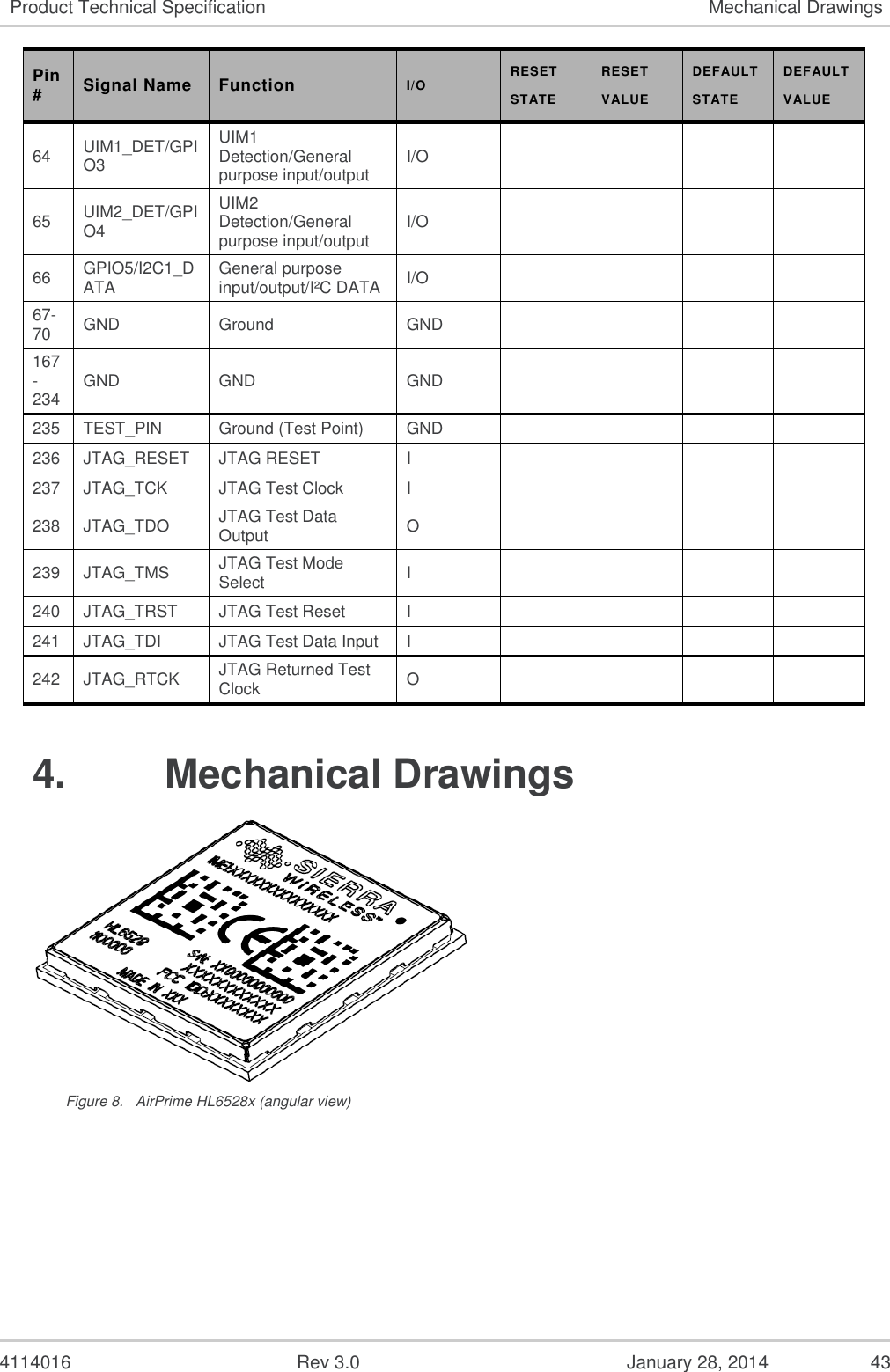
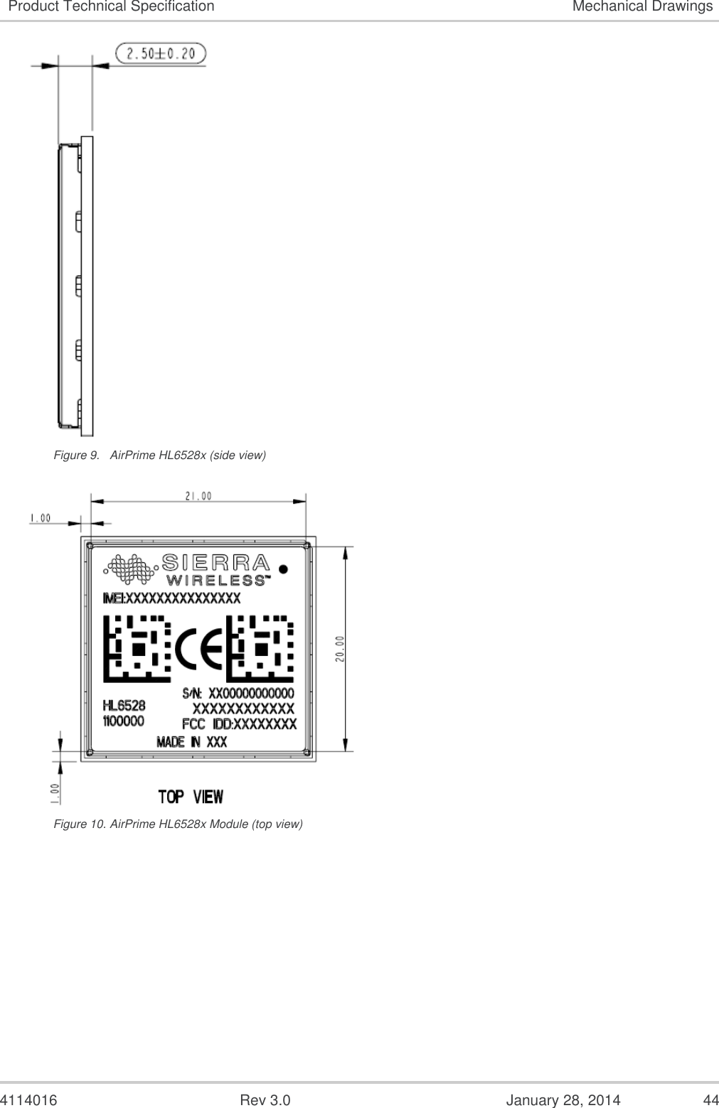
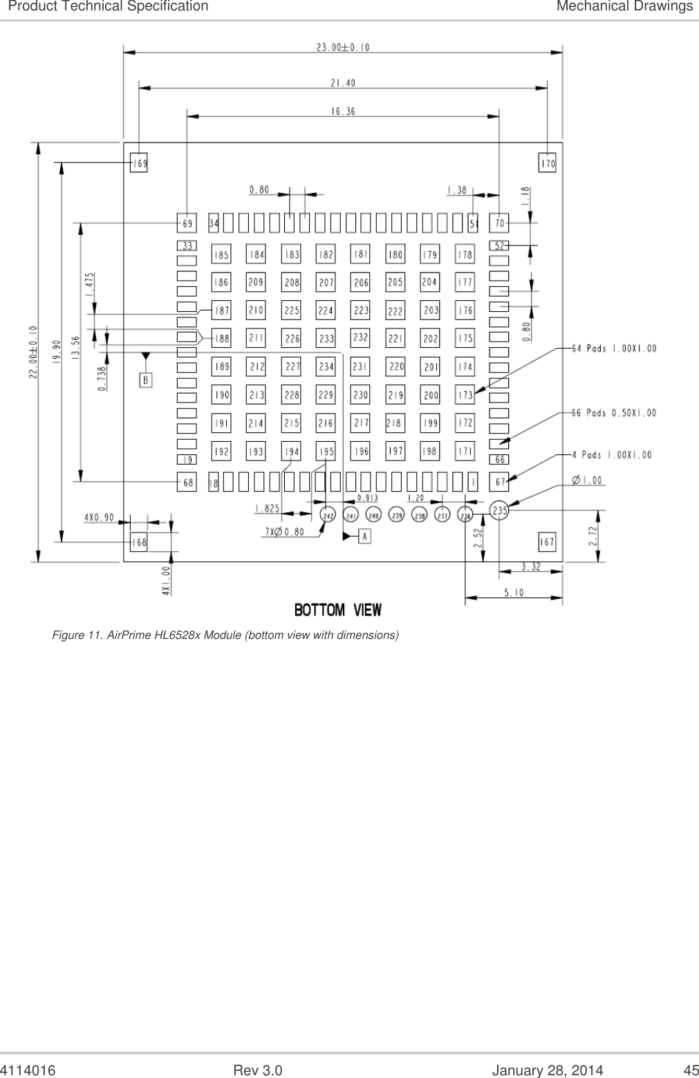
AirPrime - HL6528x - Product Technical Specification
Navigation menu
Upload a User Manual
Namespaces
Wiki Guide
HTML
PDF
Info
Views
User Manual
Discussion / Help
Navigation
![4114016 Rev 3.0 January 28, 2014 17 Product Technical Specification Introduction 1.10.3. RoHS Directive Compliant The AirPrime HL6528x module is compliant with RoHS Directive 2011/65/EU which sets limits for the use of certain restricted hazardous substances. This directive states that “from 1st July 2006, new electrical and electronic equipment put on the market does not contain lead, mercury, cadmium, hexavalent chromium, polybrominated biphenyls (PBB) or polybrominated diphenyl ethers (PBDE)”. 1.10.4. Disposing of the Product This electronic product is subject to the EU Directive 2012/19/EU for Waste Electrical and Electronic Equipment (WEEE). As such, this product must not be disposed of at a municipal waste collection point. Please refer to local regulations for directions on how to dispose of this product in an environmental friendly manner. 1.10.5. References [1] AirPrime HL Series Customer Process Guidelines Reference Number: 4114330 [2] AirPrime HL6 and HL8 Series AT Commands Interface Guide Reference Number: 4114680](https://usermanual.wiki/Sierra-Wireless/HL6528G28V/User-Guide-2285936-Page-17.png)
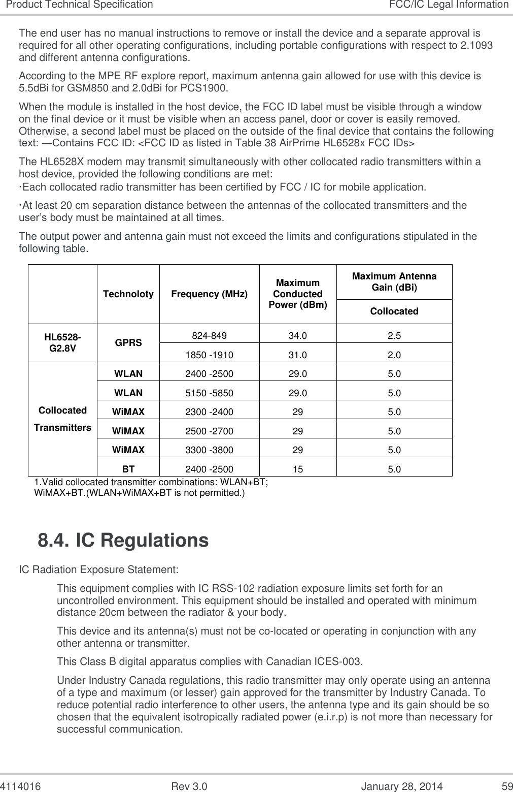
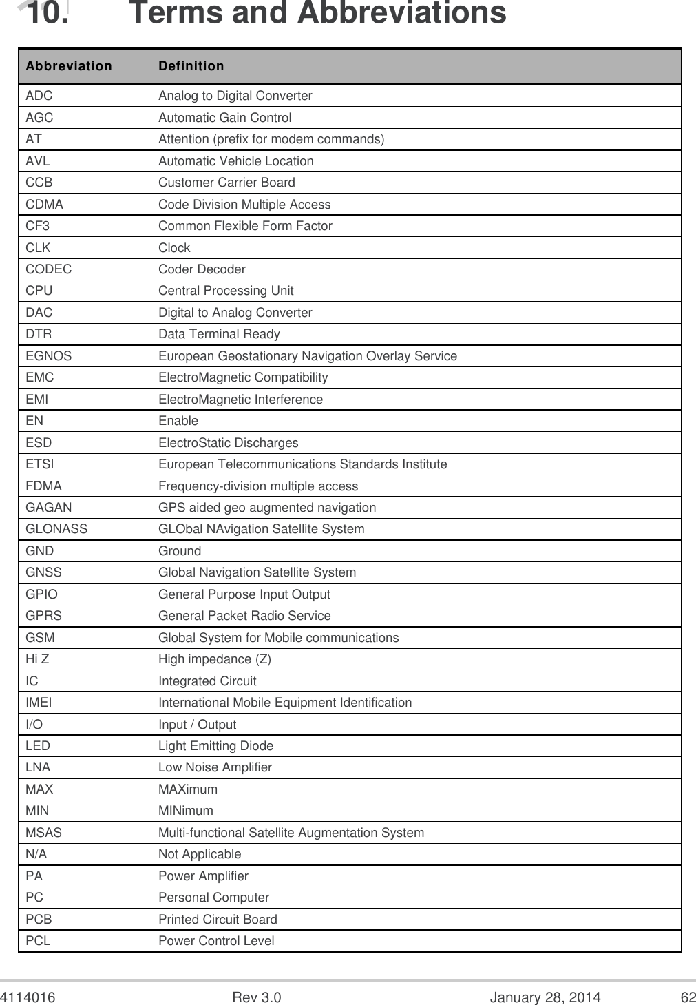
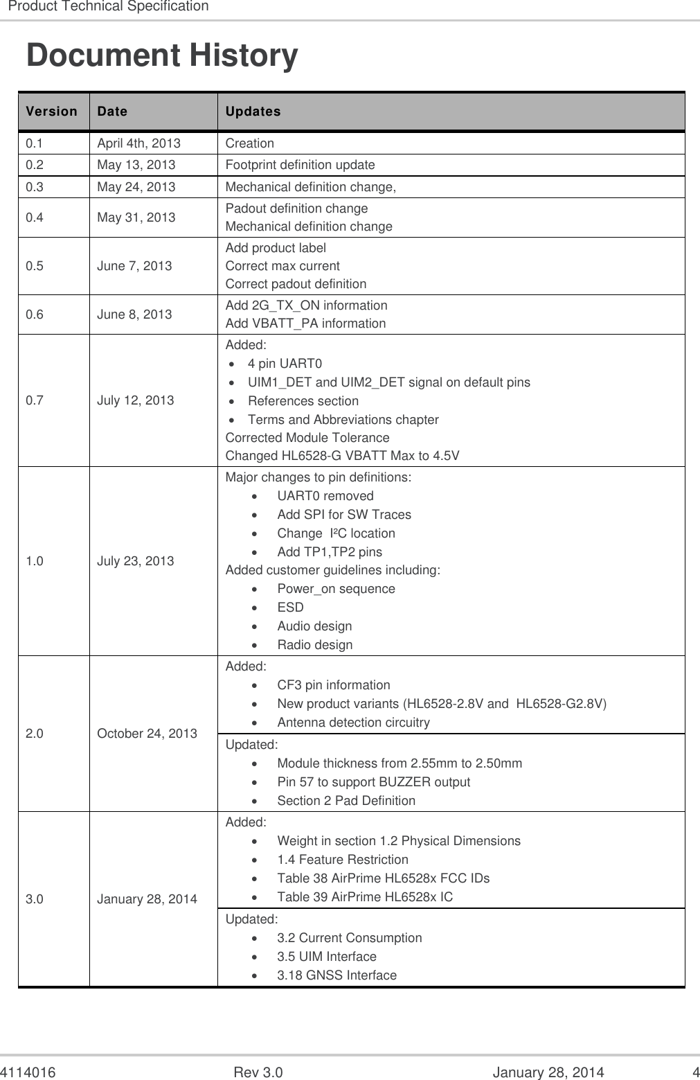
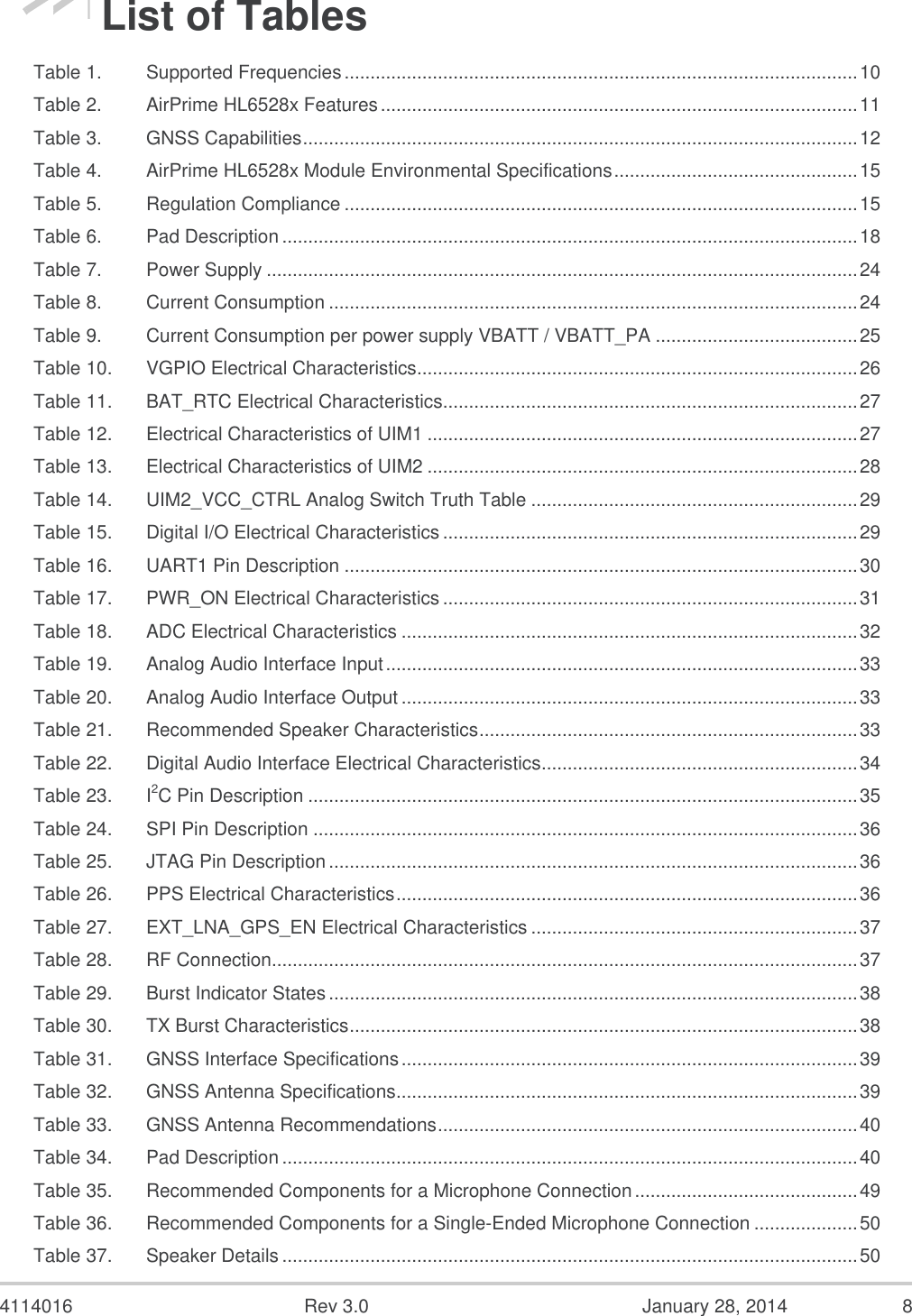
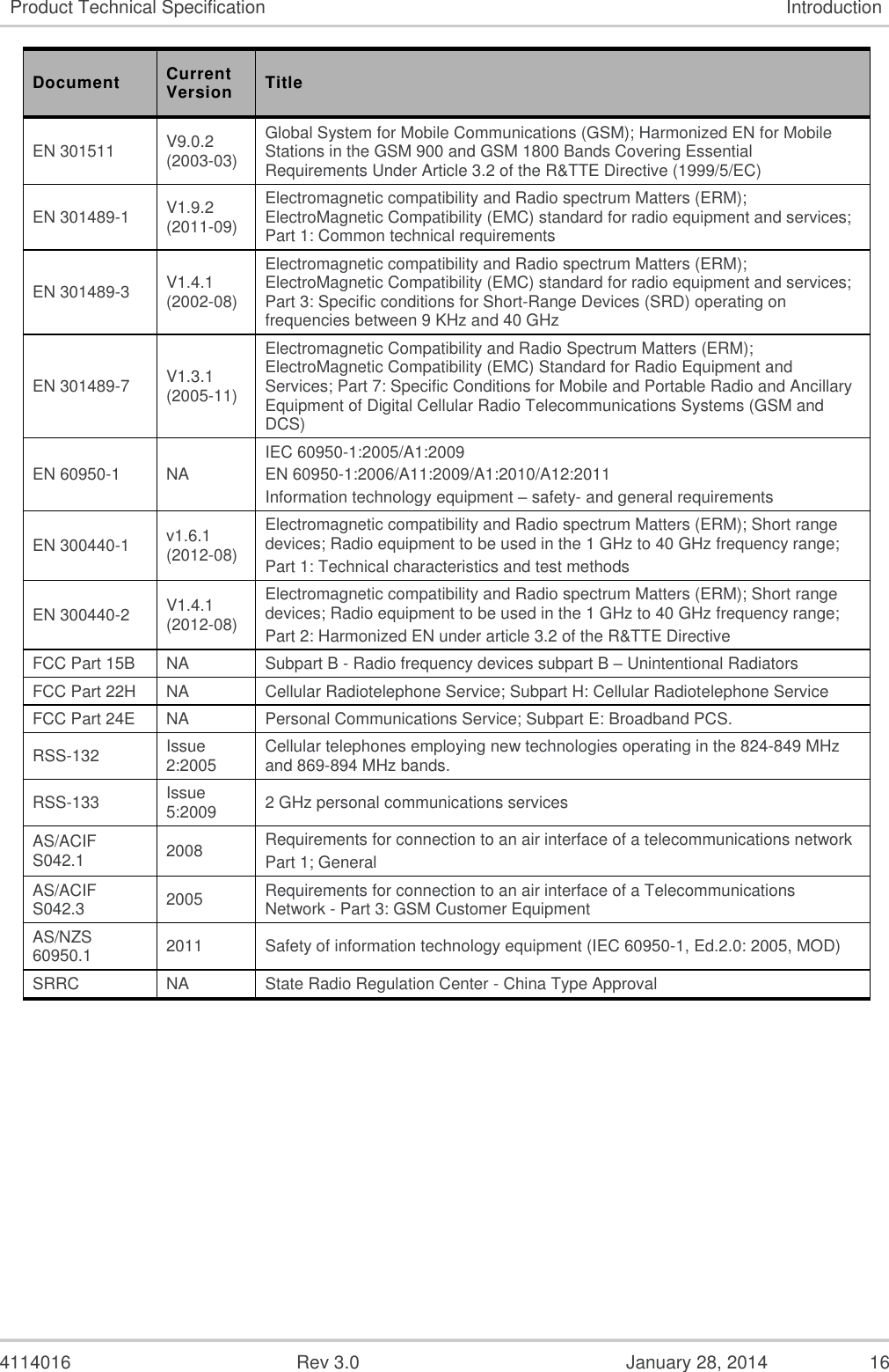
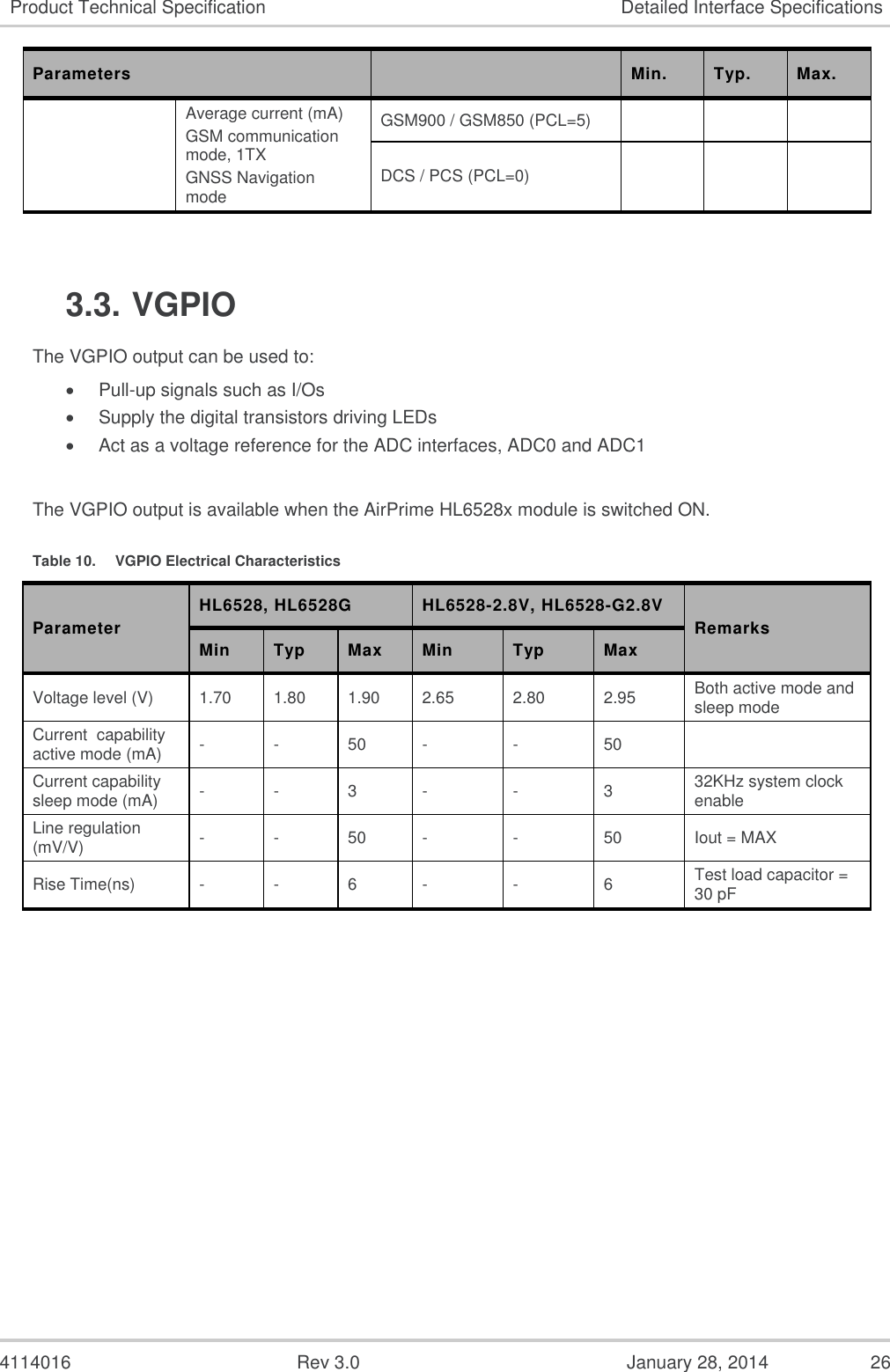
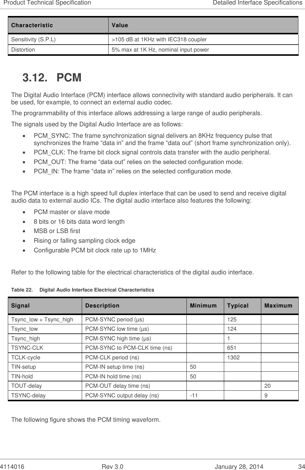
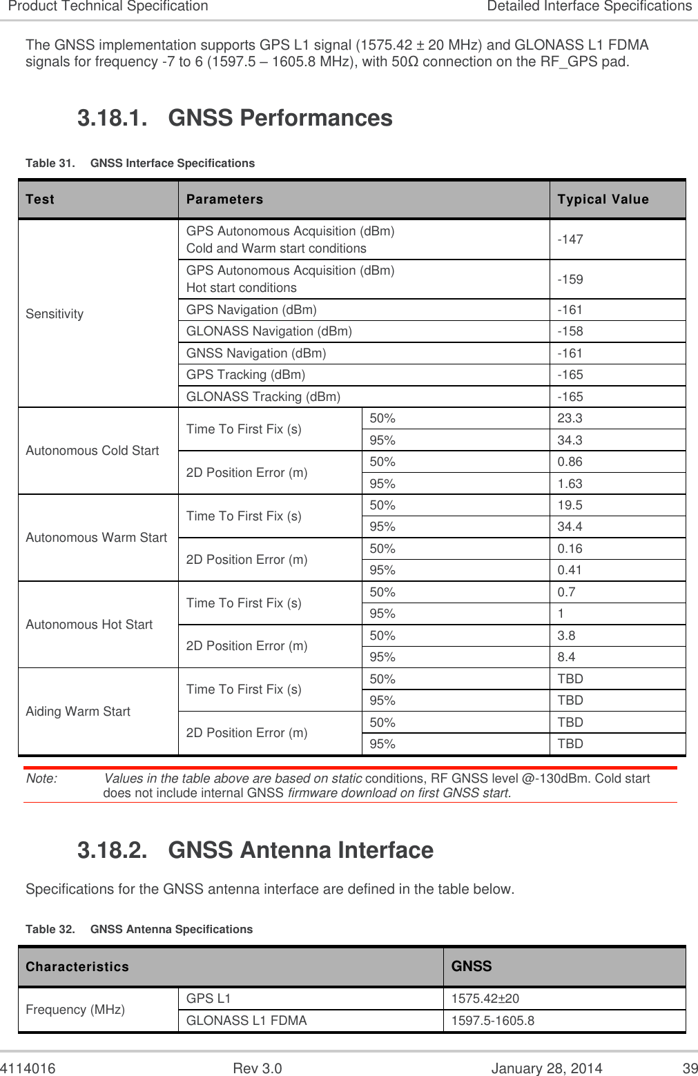
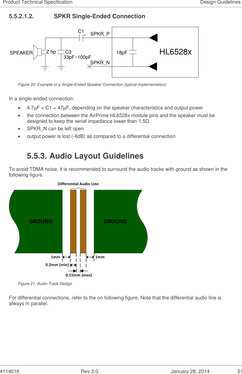
![4114016 Rev 3.0 January 28, 2014 25 Product Technical Specification Detailed Interface Specifications Parameters Min. Typ. Max. Peak Current consumption (A) GSM900 / GSM850 TBD 1.50 TBD DCS / PCS TBD 0.90 TBD GNSS Acquisition1 (mA) GSM registered on network Max value3 43 51 64 Min value4 TBD 28 TBD GNSS Navigation (1Hz)1 (mA) GSM registered on network Max value3 39 45 57 Min value4 TBD 25 TBD GNSS Navigation (1Hz)1 (mA) GSM in Flight mode Max value3 TBD TBD Min value4 TBD TBD GNSS Hibernate mode2 (mA) GSM registered on network Max value3 18 20 26 Min value4 TBD 1.5 TBD 1 Maximum SVs in view, signal level @-130dBm, high gain configuration 2 Hot start conditions are maintained in Hibernate mode3 Baseband is running (or no sleep mode allowed) in max value condition. Refer to document [2] AirPrime HL6 and HL8 Series AT Commands Interface Guide for sleep mode description. 4 Baseband is in sleep mode in min value condition. Refer to document [2] AirPrime HL6 and HL8 Series AT Commands Interface Guide for sleep mode description. Table 9. Current Consumption per power supply VBATT / VBATT_PA Parameters Min. Typ. Max. VBATT_PA Peak current (A) GSM communication mode, 2TX GSM900 / GSM850 (PCL=5) DCS / PCS (PCL=0) Peak current (A) GSM communication mode, 1TX GSM900 / GSM850 (PCL=5) 1.30 DCS / PCS (PCL=0) 0.80 Average current (mA) GSM communication mode, 1TX GSM900 / GSM850 (PCL=5) 150 DCS / PCS (PCL=0) 90 VBATT (HL6528 and HL6528-2.8V) Peak current (A) GSM communication mode, 2TX GSM900 / GSM850 (PCL=5) DCS / PCS (PCL=0) Peak current (A) GSM communication mode, 1TX GSM900 / GSM850 (PCL=5) 290 DCS / PCS (PCL=0) 125 Average current (mA) GSM communication mode, 1TX GSM900 / GSM850 (PCL=5) 70 DCS / PCS (PCL=0) 70 VBATT (HL6528-G and HL6528-G2.8V) Peak current (A) GSM communication mode, 2TX GNSS Navigation mode GSM900 / GSM850 (PCL=5) DCS / PCS (PCL=0) Peak current (A) GSM communication mode, 1TX GNSS Navigation mode GSM900 / GSM850 (PCL=5) DCS / PCS (PCL=0)](https://usermanual.wiki/Sierra-Wireless/HL6528G28V/User-Guide-2285936-Page-25.png)
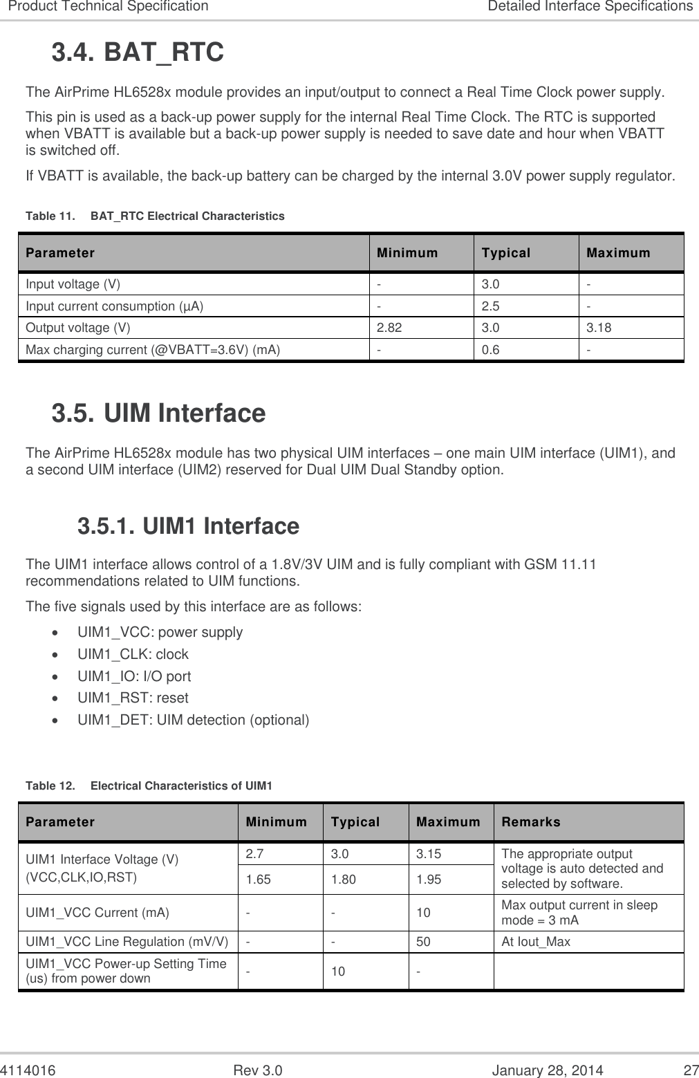
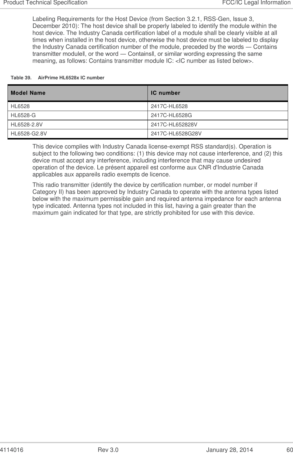
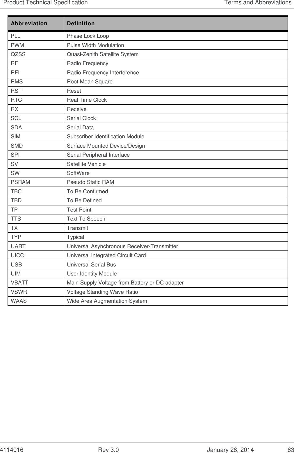
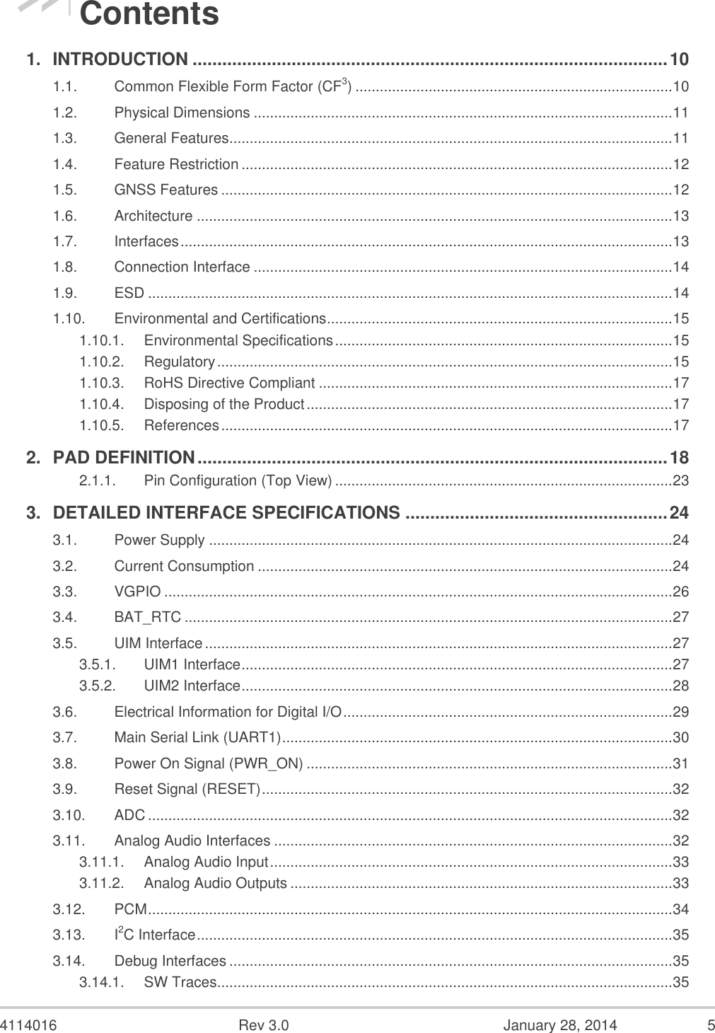
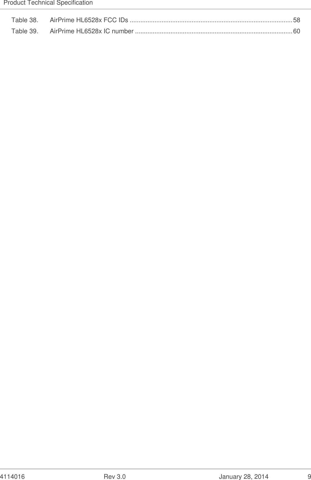
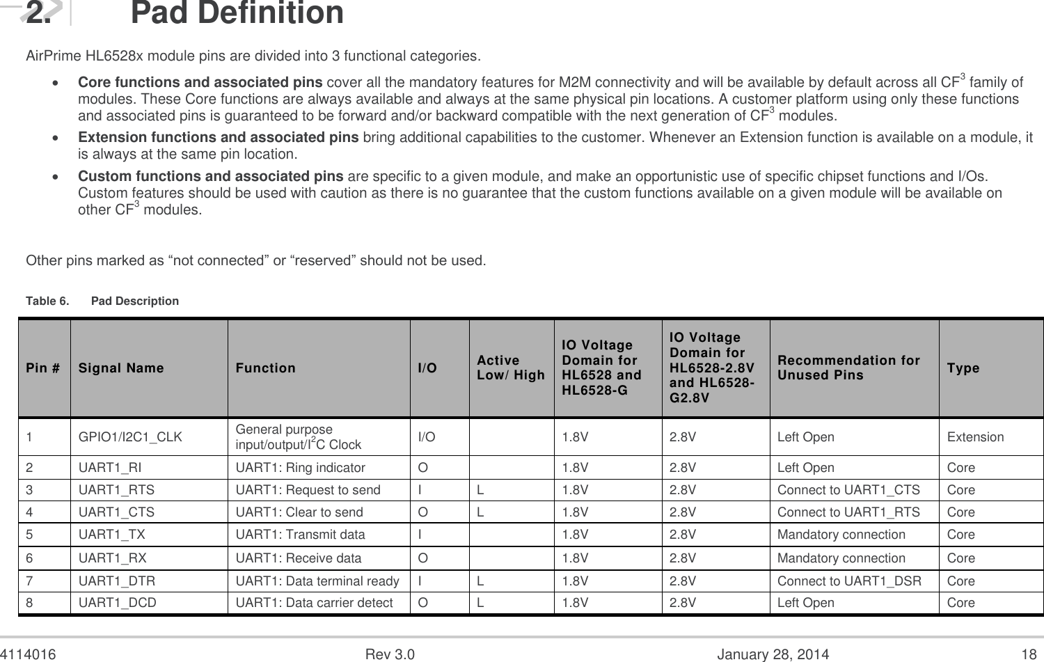
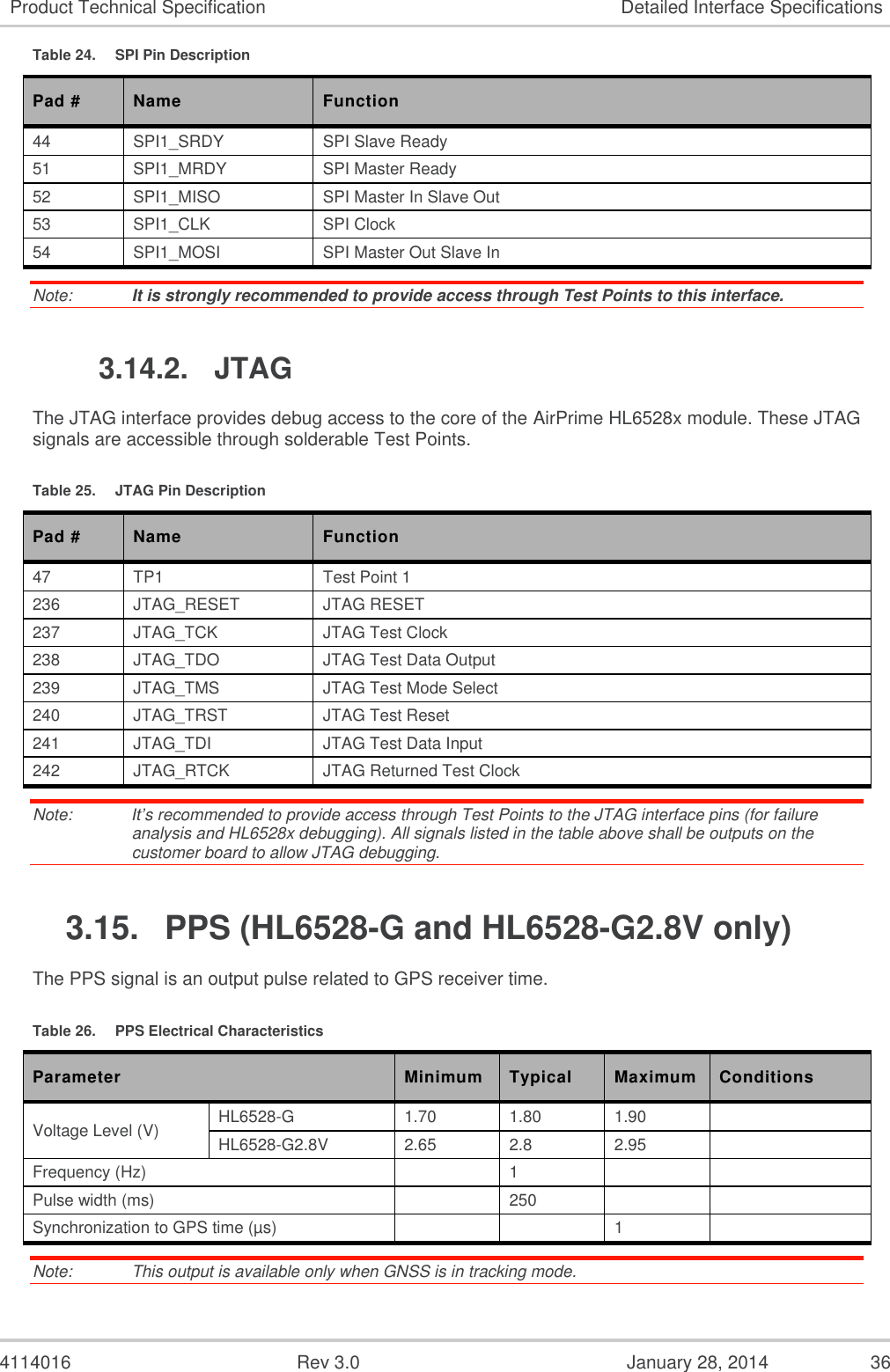
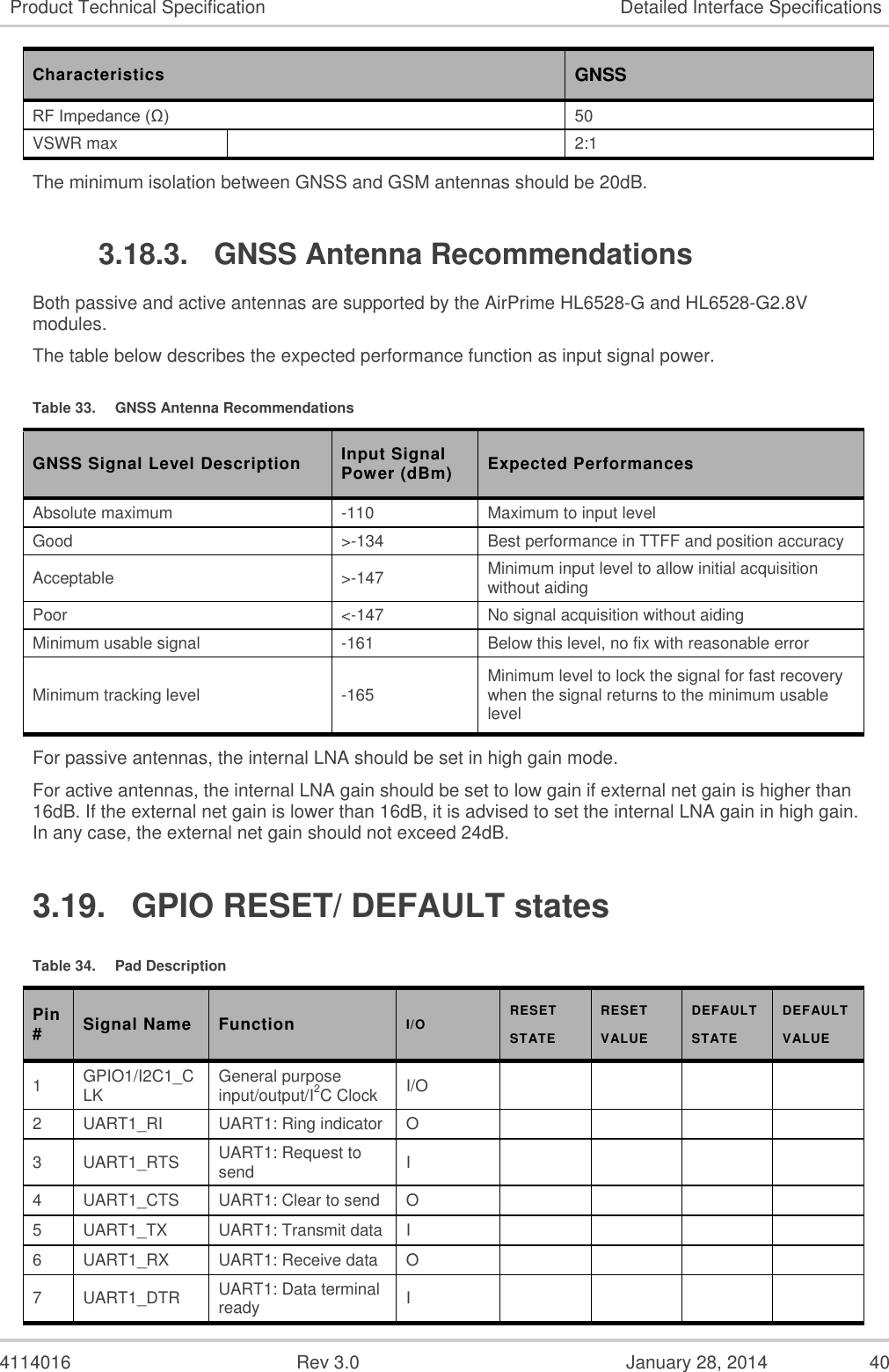
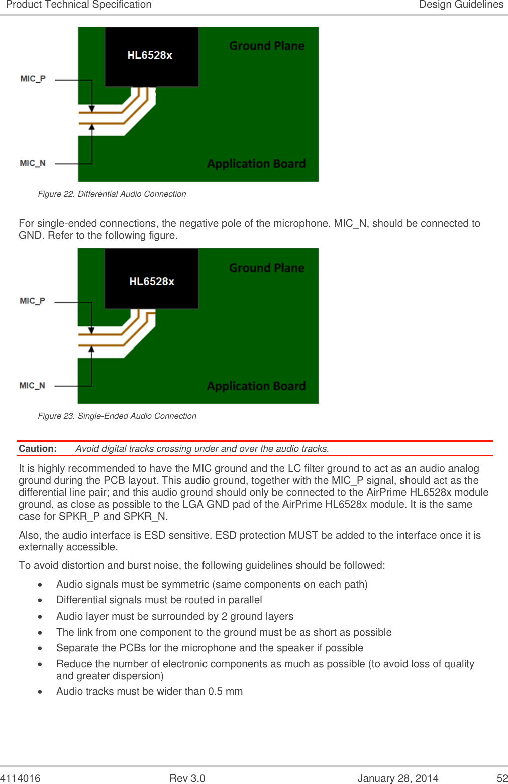
![4114016 Rev 3.0 January 28, 2014 35 Product Technical Specification Detailed Interface Specifications Figure 6. PCM Timing Waveform 3.13. I2C Interface NMEA frames can be output from the UART or through a dedicated serial port (I2C). Table 23. I2C Pin Description Pad # Name Function 1 I2C1_CLK I2C Serial Clock Line 66 I2C1_DATA I2C Serial Data Line Note: I2C pins are multiplexed with GPIO features. The main characteristics of the I2C interface are as follows: Master mode (I2C1_CLK is an output of the AirPrime HL6528x module) I2C clock is set at 400KHz As AirPrime HL6528x module is master only, devices connected to the I2C bus shall be slave devices. In order for AirPrime HL6528x module to communicate with the slave device, the slave 7-bit address shall be loaded inside the module before activating the GPS NMEA output. See [2] for AT command description. 3.14. Debug Interfaces The AirPrime HL6528x module provides two interfaces for a powerful debug system. 3.14.1. SW Traces The AirPrime HL6528x module provides a SW TRACE interface, providing real-time instruction and data trace of the modem core. The SW TRACE interface is accessible through the SPI port.](https://usermanual.wiki/Sierra-Wireless/HL6528G28V/User-Guide-2285936-Page-35.png)
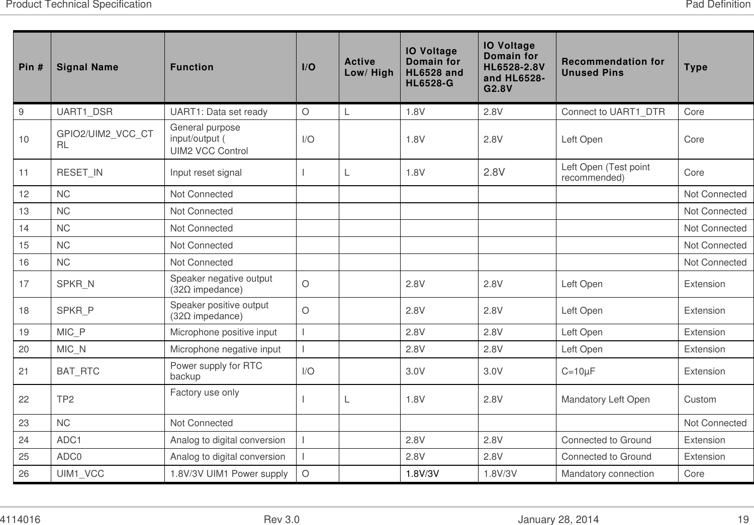
![4114016 Rev 3.0 January 28, 2014 57 6. X-Ray Exposure X-ray exposure results in an undesirable shift in programmed bit threshold voltage of the Flash memory. As a result, Sierra Wireless recommends avoiding any X-ray exposure during customer manufacturing process to ensure software integrity and long term reliability. In case X- ray inspection could not be eliminated from the customer manufacturing process, a variety of mitigation methods should be implemented to lower the risk of potential failure: Use of filter between source and module to minimize exposure to harmful soft X- ray 300µm Zn filter or 1mm Al filter are optimal Zn and Al absorb soft X-ray to which silicon is particularly vulnerable, and transmit soft and medium energy X-rays required to obtain good imaging Minimize X-Ray dose should be less than 10 RADs KV peak should be less than 50KV peak tube current should be less than 20µA Maximize distance between source and the module Minimize the X-ray time use the shortest exposure time possible sampling only, not 100% inspection Note that these mitigation guidelines are for information only as it’s NOT possible to provide accurate acceptable or unacceptable X- ray exposure criteria, e.g. maximum safe dose rate, maximum safe exposure time, etc. 7. Flash memory endurance As many embedded device, the AirPrime HL6528x module is using flash memory which are guaranteed for a limited number of program/erasing cycles per sector (100,000 cycles). Although state-of-the-art mechanism has been implemented to limit the number of writing/erasing cycles, Sierra Wireless recommends using “writing” AT commands appropriately and with caution. Those AT commands are identified in the AirPrime HL6 and HL8 Series AT Commands Interface Guide [2]. 8. FCC/IC Legal Information 8.1. Label The AirPrime HL6528x module is labeled with its own FCC ID on the shield side. Each HL6528x variant has its own FCC ID as listed in the table below.](https://usermanual.wiki/Sierra-Wireless/HL6528G28V/User-Guide-2285936-Page-57.png)