Sierra Wireless HL6528G28V Wireless Module User Manual Product Technical Specification
Sierra Wireless Inc. Wireless Module Product Technical Specification
AirPrime - HL6528x - Product Technical Specification

4114016
3.0
January 28, 2014
AirPrime HL6528x
Product Technical Specification

4114016 Rev 3.0 January 28, 2014 2
Product Technical Specification
Important Notice
Due to the nature of wireless communications, transmission and reception of data can never be
guaranteed. Data may be delayed, corrupted (i.e., have errors) or be totally lost. Although significant
delays or losses of data are rare when wireless devices such as the Sierra Wireless modem are used
in a normal manner with a well-constructed network, the Sierra Wireless modem should not be used
in situations where failure to transmit or receive data could result in damage of any kind to the user or
any other party, including but not limited to personal injury, death, or loss of property. Sierra Wireless
accepts no responsibility for damages of any kind resulting from delays or errors in data transmitted or
received using the Sierra Wireless modem, or for failure of the Sierra Wireless modem to transmit or
receive such data.
Safety and Hazards
Do not operate the Sierra Wireless modem in areas where cellular modems are not advised without
proper device certifications. These areas include environments where cellular radio can interfere such
as explosive atmospheres, medical equipment, or any other equipment which may be susceptible to
any form of radio interference. The Sierra Wireless modem can transmit signals that could interfere
with this equipment. Do not operate the Sierra Wireless modem in any aircraft, whether the aircraft is
on the ground or in flight. In aircraft, the Sierra Wireless modem MUST BE POWERED OFF. When
operating, the Sierra Wireless modem can transmit signals that could interfere with various onboard
systems.
Note: Some airlines may permit the use of cellular phones while the aircraft is on the ground and the door
is open. Sierra Wireless modems may be used at this time.
The driver or operator of any vehicle should not operate the Sierra Wireless modem while in control of
a vehicle. Doing so will detract from the driver or operator’s control and operation of that vehicle. In
some states and provinces, operating such communications devices while in control of a vehicle is an
offence.
Limitations of Liability
This manual is provided “as is”. Sierra Wireless makes no warranties of any kind, either expressed or
implied, including any implied warranties of merchantability, fitness for a particular purpose, or
noninfringement. The recipient of the manual shall endorse all risks arising from its use.
The information in this manual is subject to change without notice and does not represent a
commitment on the part of Sierra Wireless. SIERRA WIRELESS AND ITS AFFILIATES
SPECIFICALLY DISCLAIM LIABILITY FOR ANY AND ALL DIRECT, INDIRECT, SPECIAL,
GENERAL, INCIDENTAL, CONSEQUENTIAL, PUNITIVE OR EXEMPLARY DAMAGES INCLUDING,
BUT NOT LIMITED TO, LOSS OF PROFITS OR REVENUE OR ANTICIPATED PROFITS OR
REVENUE ARISING OUT OF THE USE OR INABILITY TO USE ANY SIERRA WIRELESS
PRODUCT, EVEN IF SIERRA WIRELESS AND/OR ITS AFFILIATES HAS BEEN ADVISED OF THE
POSSIBILITY OF SUCH DAMAGES OR THEY ARE FORESEEABLE OR FOR CLAIMS BY ANY
THIRD PARTY.
Notwithstanding the foregoing, in no event shall Sierra Wireless and/or its affiliates aggregate liability
arising under or in connection with the Sierra Wireless product, regardless of the number of events,
occurrences, or claims giving rise to liability, be in excess of the price paid by the purchaser for the
Sierra Wireless product.
Customer understands that Sierra Wireless is not providing cellular or GPS (including A-GPS)
services. These services are provided by a third party and should be purchased directly by the
Customer.

4114016 Rev 3.0 January 28, 2014 3
Product Technical Specification
SPECIFIC DISCLAIMERS OF LIABILITY: CUSTOMER RECOGNIZES AND ACKNOWLEDGES
SIERRA WIRELESS IS NOT RESPONSIBLE FOR AND SHALL NOT BE HELD LIABLE FOR ANY
DEFECT OR DEFICIENCY OF ANY KIND OF CELLULAR OR GPS (INCLUDING A-GPS)
SERVICES.
Patents
This product may contain technology developed by or for Sierra Wireless Inc.
This product includes technology licensed from QUALCOMM®.
This product is manufactured or sold by Sierra Wireless Inc. or its affiliates under one or more patents
licensed from InterDigital Group and MMP Portfolio Licensing.
Copyright
© 2014 Sierra Wireless. All rights reserved.
Trademarks
Sierra Wireless®, AirPrime®, AirLink®, AirVantage®, WISMO® and the Sierra Wireless and Open AT
logos are registered trademarks of Sierra Wireless, Inc. or one of its subsidiaries.
Watcher® is a registered trademark of NETGEAR, Inc., used under license.
Windows® and Windows Vista® are registered trademarks of Microsoft Corporation.
Macintosh® and Mac OS X® are registered trademarks of Apple Inc., registered in the U.S. and other
countries.
QUALCOMM® is a registered trademark of QUALCOMM Incorporated. Used under license.
Other trademarks are the property of their respective owners.
Contact Information
Sales Desk:
Phone:
1-604-232-1488
Hours:
8:00 AM to 5:00 PM Pacific Time
Contact:
http://www.sierrawireless.com/sales
Post:
Sierra Wireless
13811 Wireless Way
Richmond, BC
Canada V6V 3A4
Technical Support:
support@sierrawireless.com
RMA Support:
repairs@sierrawireless.com
Fax:
1-604-231-1109
Web:
http://www.sierrawireless.com/
Consult our website for up-to-date product descriptions, documentation, application notes, firmware
upgrades, troubleshooting tips, and press releases: www.sierrawireless.com
4114016 Rev 3.0 January 28, 2014 4
Product Technical Specification
Document History
Version
Date
Updates
0.1
April 4th, 2013
Creation
0.2
May 13, 2013
Footprint definition update
0.3
May 24, 2013
Mechanical definition change,
0.4
May 31, 2013
Padout definition change
Mechanical definition change
0.5
June 7, 2013
Add product label
Correct max current
Correct padout definition
0.6
June 8, 2013
Add 2G_TX_ON information
Add VBATT_PA information
0.7
July 12, 2013
Added:
4 pin UART0
UIM1_DET and UIM2_DET signal on default pins
References section
Terms and Abbreviations chapter
Corrected Module Tolerance
Changed HL6528-G VBATT Max to 4.5V
1.0
July 23, 2013
Major changes to pin definitions:
UART0 removed
Add SPI for SW Traces
Change I²C location
Add TP1,TP2 pins
Added customer guidelines including:
Power_on sequence
ESD
Audio design
Radio design
2.0
October 24, 2013
Added:
CF3 pin information
New product variants (HL6528-2.8V and HL6528-G2.8V)
Antenna detection circuitry
Updated:
Module thickness from 2.55mm to 2.50mm
Pin 57 to support BUZZER output
Section 2 Pad Definition
3.0
January 28, 2014
Added:
Weight in section 1.2 Physical Dimensions
1.4 Feature Restriction
Table 38 AirPrime HL6528x FCC IDs
Table 39 AirPrime HL6528x IC
Updated:
3.2 Current Consumption
3.5 UIM Interface
3.18 GNSS Interface

4114016 Rev 3.0 January 28, 2014 5
Contents
1. INTRODUCTION ................................................................................................ 10
1.1. Common Flexible Form Factor (CF3) .............................................................................. 10
1.2. Physical Dimensions ....................................................................................................... 11
1.3. General Features ............................................................................................................. 11
1.4. Feature Restriction .......................................................................................................... 12
1.5. GNSS Features ............................................................................................................... 12
1.6. Architecture ..................................................................................................................... 13
1.7. Interfaces ......................................................................................................................... 13
1.8. Connection Interface ....................................................................................................... 14
1.9. ESD ................................................................................................................................. 14
1.10. Environmental and Certifications ..................................................................................... 15
1.10.1. Environmental Specifications ................................................................................... 15
1.10.2. Regulatory ................................................................................................................ 15
1.10.3. RoHS Directive Compliant ....................................................................................... 17
1.10.4. Disposing of the Product .......................................................................................... 17
1.10.5. References ............................................................................................................... 17
2. PAD DEFINITION ............................................................................................... 18
2.1.1. Pin Configuration (Top View) ................................................................................... 23
3. DETAILED INTERFACE SPECIFICATIONS ..................................................... 24
3.1. Power Supply .................................................................................................................. 24
3.2. Current Consumption ...................................................................................................... 24
3.3. VGPIO ............................................................................................................................. 26
3.4. BAT_RTC ........................................................................................................................ 27
3.5. UIM Interface ................................................................................................................... 27
3.5.1. UIM1 Interface .......................................................................................................... 27
3.5.2. UIM2 Interface .......................................................................................................... 28
3.6. Electrical Information for Digital I/O ................................................................................. 29
3.7. Main Serial Link (UART1) ................................................................................................ 30
3.8. Power On Signal (PWR_ON) .......................................................................................... 31
3.9. Reset Signal (RESET) ..................................................................................................... 32
3.10. ADC ................................................................................................................................. 32
3.11. Analog Audio Interfaces .................................................................................................. 32
3.11.1. Analog Audio Input ................................................................................................... 33
3.11.2. Analog Audio Outputs .............................................................................................. 33
3.12. PCM ................................................................................................................................. 34
3.13. I2C Interface ..................................................................................................................... 35
3.14. Debug Interfaces ............................................................................................................. 35
3.14.1. SW Traces ................................................................................................................ 35

4114016 Rev 3.0 January 28, 2014 6
Product Technical Specification
3.14.2. JTAG ........................................................................................................................ 36
3.15. PPS (HL6528-G and HL6528-G2.8V only)...................................................................... 36
3.16. EXT_LNA_GPS_EN (HL6528-G and HL6528-G2.8V only) ............................................ 37
3.17. RF Interface ..................................................................................................................... 37
3.17.1. RF Connection ......................................................................................................... 37
3.17.2. RF Performances ..................................................................................................... 37
3.17.3. TX Burst Indicator (2G_TX_ON) .............................................................................. 37
3.18. GNSS Interface ............................................................................................................... 38
3.18.1. GNSS Performances ................................................................................................ 39
3.18.2. GNSS Antenna Interface .......................................................................................... 39
3.18.3. GNSS Antenna Recommendations ......................................................................... 40
3.19. GPIO RESET/ DEFAULT states ..................................................................................... 40
4. MECHANICAL DRAWINGS ............................................................................... 43
5. DESIGN GUIDELINES ....................................................................................... 46
5.1. Power-Up Sequence ....................................................................................................... 46
5.2. Module Switch-Off ........................................................................................................... 46
5.3. Sleep Mode Management ............................................................................................... 47
5.4. ESD Guidelines for UIM Cards ........................................................................................ 47
5.5. Audio Integration ............................................................................................................. 48
5.5.1. Microphone Audio Design ........................................................................................ 48
5.5.2. Speaker Audio Design ............................................................................................. 50
5.5.3. Audio Layout Guidelines .......................................................................................... 51
5.6. Radio Integration ............................................................................................................. 53
5.6.1. RF Routing Recommendations ................................................................................ 53
5.6.2. GSM Antenna Integration with Antenna Detection Circuitry .................................... 55
5.6.3. GNSS Active Antenna Integration ............................................................................ 56
6. X-RAY EXPOSURE ............................................................................................ 57
7. FLASH MEMORY ENDURANCE ....................................................................... 57
8. FCC/IC LEGAL INFORMATION ......................................................................... 57
8.1. Label ................................................................................................................................ 57
8.2. FCC Regulations ............................................................................................................. 58
8.3. RF Exposure Information ................................................................................................ 58
8.4. IC Regulations ................................................................................................................. 59
9. ORDERING INFORMATION .............................................................................. 61
10. TERMS AND ABBREVIATIONS ........................................................................ 62

4114016 Rev 3.0 January 28, 2014 7
List of Figures
Figure 1. AirPrime HL6528x Architecture Overview ....................................................................... 13
Figure 2. AirPrime HL6528x Module Mechanical Overview ........................................................... 14
Figure 3. Pin Configuration ............................................................................................................. 23
Figure 4. UIM2 with an Analog Switch ............................................................................................ 29
Figure 5. PWR_ON Sequence ....................................................................................................... 31
Figure 6. PCM Timing Waveform ................................................................................................... 35
Figure 7. 2G_TX_ON State during TX Burst .................................................................................. 38
Figure 8. AirPrime HL6528x (angular view) .................................................................................... 43
Figure 9. AirPrime HL6528x (side view) ......................................................................................... 44
Figure 10. AirPrime HL6528x Module (top view) .............................................................................. 44
Figure 11. AirPrime HL6528x Module (bottom view with dimensions) ............................................. 45
Figure 12. UART Signals during the Power ON Sequence .............................................................. 46
Figure 13. Power OFF Sequence for PWR_ON, VGPIO and CTS .................................................. 46
Figure 14. EMC and ESD Components Close to the UIM ................................................................ 47
Figure 15. Example of a MIC Input Connection with LC Filter ......................................................... 48
Figure 16. Example of a MIC Input Connection without LC Filter .................................................... 48
Figure 17. Example of a Single-Ended MIC Input Connection with LC Filter ................................... 49
Figure 18. Example of a Single-Ended MIC Input Connection without LC Filter .............................. 49
Figure 19. Example of a Differential Connection for SPKR .............................................................. 50
Figure 20. Example of a Single-Ended Speaker Connection (typical implementation) .................... 51
Figure 21. Audio Track Design ......................................................................................................... 51
Figure 22. Differential Audio Connection .......................................................................................... 52
Figure 23. Single-Ended Audio Connection ..................................................................................... 52
Figure 24. AppCAD Screenshot for Microstrip Design Power Mode Diagram ................................. 53
Figure 25. RF Routing Examples ..................................................................................................... 54
Figure 26. Coplanar Clearance Example ......................................................................................... 54
Figure 27. Antenna Microstrip Routing Example .............................................................................. 55
Figure 28. GSM Antenna Connection with Antenna Detection ........................................................ 55
Figure 29. GNSS Application with Active Antenna ........................................................................... 56

4114016 Rev 3.0 January 28, 2014 8
List of Tables
Table 1. Supported Frequencies ................................................................................................... 10
Table 2. AirPrime HL6528x Features ............................................................................................ 11
Table 3. GNSS Capabilities ........................................................................................................... 12
Table 4. AirPrime HL6528x Module Environmental Specifications ............................................... 15
Table 5. Regulation Compliance ................................................................................................... 15
Table 6. Pad Description ............................................................................................................... 18
Table 7. Power Supply .................................................................................................................. 24
Table 8. Current Consumption ...................................................................................................... 24
Table 9. Current Consumption per power supply VBATT / VBATT_PA ....................................... 25
Table 10. VGPIO Electrical Characteristics ..................................................................................... 26
Table 11. BAT_RTC Electrical Characteristics................................................................................ 27
Table 12. Electrical Characteristics of UIM1 ................................................................................... 27
Table 13. Electrical Characteristics of UIM2 ................................................................................... 28
Table 14. UIM2_VCC_CTRL Analog Switch Truth Table ............................................................... 29
Table 15. Digital I/O Electrical Characteristics ................................................................................ 29
Table 16. UART1 Pin Description ................................................................................................... 30
Table 17. PWR_ON Electrical Characteristics ................................................................................ 31
Table 18. ADC Electrical Characteristics ........................................................................................ 32
Table 19. Analog Audio Interface Input ........................................................................................... 33
Table 20. Analog Audio Interface Output ........................................................................................ 33
Table 21. Recommended Speaker Characteristics ......................................................................... 33
Table 22. Digital Audio Interface Electrical Characteristics ............................................................. 34
Table 23. I2C Pin Description .......................................................................................................... 35
Table 24. SPI Pin Description ......................................................................................................... 36
Table 25. JTAG Pin Description ...................................................................................................... 36
Table 26. PPS Electrical Characteristics ......................................................................................... 36
Table 27. EXT_LNA_GPS_EN Electrical Characteristics ............................................................... 37
Table 28. RF Connection................................................................................................................. 37
Table 29. Burst Indicator States ...................................................................................................... 38
Table 30. TX Burst Characteristics .................................................................................................. 38
Table 31. GNSS Interface Specifications ........................................................................................ 39
Table 32. GNSS Antenna Specifications ......................................................................................... 39
Table 33. GNSS Antenna Recommendations ................................................................................. 40
Table 34. Pad Description ............................................................................................................... 40
Table 35. Recommended Components for a Microphone Connection ........................................... 49
Table 36. Recommended Components for a Single-Ended Microphone Connection .................... 50
Table 37. Speaker Details ............................................................................................................... 50

4114016 Rev 3.0 January 28, 2014 9
Product Technical Specification
Table 38. AirPrime HL6528x FCC IDs ............................................................................................ 58
Table 39. AirPrime HL6528x IC number ......................................................................................... 60
4114016 Rev 3.0 January 28, 2014 10
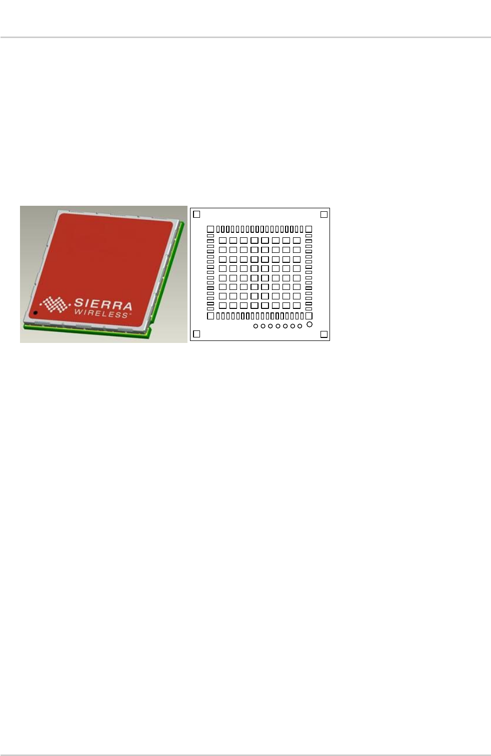
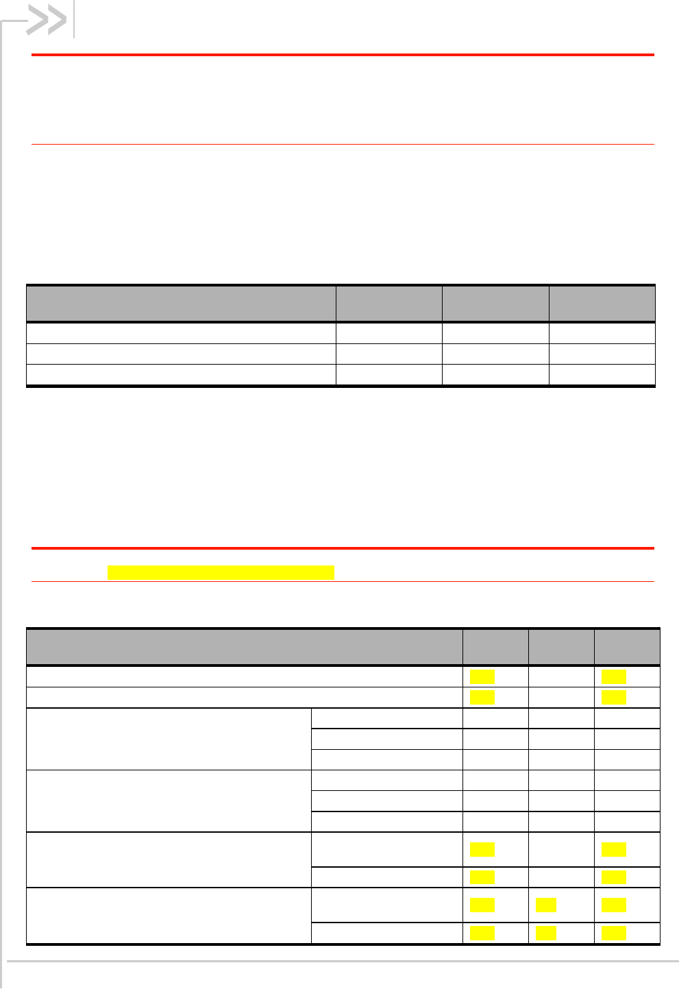
1. Introduction
This document defines the high level product features and illustrates the interfaces for the AirPrime
HL6528x series of embedded modules. This document is intended to cover the hardware aspects of
the product series, including electrical and mechanical.
Variants covered in this document are:
HL6528
HL6528-G
HL6528-2.8V
HL6528-G2.8V
The AirPrime HL6528 and HL6528-G modules are 1.8V IO modules as defined in section 2 Pad
Definition. 2.8V IO variants are also available, and defined throughout this document as HL6528-2.8V
and HL6528-G2.8V. HL6528x denotes applicability to all four variants.
The AirPrime HL6528x belongs to the AirPrime HL Series from Essential Connectivity Module family.
This is an Industrial Grade quad-band GSM/GPRS Embedded Wireless Module, designed for the
automotive market and any other market with similar quality and life-time support requirements. The
following table enumerates the frequencies supported by the HL6528x module.
Table 1. Supported Frequencies
RF Band
Transmit band (Tx)
Receive band (Rx)
Maximum Output Power
GSM 850
824 to 849 MHz
869 to 894 MHz
2 Watts GSM & GPRS
E-GSM 900
880 to 915 MHz
925 to 960 MHz
2 Watts GSM & GPRS
DCS 1800
1710 to 1785 MHz
1805 to 1880 MHz
1 Watt GSM & GPRS
PCS 1900
1850 to 1910 MHz
1930 to 1990 MHz
1 Watt GSM & GPRS
This module supports a large variety of interfaces such as Analog & Digital Audio and Dual UIM Dual
Standby to provide customers with the highest level of flexibility in implementing high-end solutions.
In addition to having the same features as AirPrime HL6528 and HL6528-2.8V modules, the AirPrime
HL6528-G and HL6528-G2.8V modules also embed a high-performance GNSS receiver.
1.1. Common Flexible Form Factor (CF3)
The AirPrime HL6528x module belongs to the Common Flexible Form Factor (CF3) family of modules.
This family consists of a series of WWAN modules that share the same mechanical dimensions (same
width and length with varying thicknesses) and footprint. The CF3 form factor provides a unique
solution to a series of problems faced commonly in the WWAN module space as it:
Accommodates multiple radio technologies (from 2G to LTE advanced) and band groupings
Supports bit-pipe (Essential Module Series) and value add (Smart Module Series) solutions
Offers electrical and functional compatibility
Provides Direct Mount as well Socketability depending on customer needs

4114016 Rev 3.0 January 28, 2014 11
Product Technical Specification
Introduction
1.2. Physical Dimensions
The AirPrime HL6528x modules are compact size, robust, fully shielded modules with:
Length: 23 mm
Width: 22 mm
Thickness: 2.50 mm (including the label)
Weight : 2.25g
Note: Dimensions specified above are typical values.
1.3. General Features
The table below summarizes the AirPrime HL6528x module features.
Table 2. AirPrime HL6528x Features
Feature
Description
GSM/DCS Output
Power
Class 4 (2 W) for GSM 850 and E-GSM
Class 1 (1 W) for DCS and PCS
GPRS
Quad-band GSM850/E-GSM/DCS/PCS
GPRS Multi-slot class 10
R99 support
PBCCH support
Coding schemes: CS1 to CS4
Audio Interface
Analog and Digital interfaces
Supports Full Rate (FR), Enhanced Full Rate (EFR), Half Rate (HR) and
Adaptive Multi Rate (AMR)
Noise reduction and echo cancellation
DTMF generation
UIM Interface
Dual UIM Dual Standby support
1.8V/3.0V support for UIM1
3V interface for UIM2
Supports UIM application tool kit with proactive UIM commands
Application Interface
Full set of AT commands for GSM/GPRS including GSM 07.07 and 07.05
AT command sets
Comprehensive set of dedicated AT commands for M2M applications
SMS
SMS class 0,1 and 2
SMS MT, MO
SMS storage into UIM card or Flash memory
Concatenation of MT SMS
Supplementary
Services
Call Forwarding
Call Barring
Multiparty Service
Call Waiting
Call Hold
USSD
Automatic answer
4114016 Rev 3.0 January 28, 2014 12
Product Technical Specification
Introduction
Feature
Description
RTC
Real Time Clock (RTC) with calendar and alarm
Temperature Sensor
Temperature monitoring
Alarms
1.4. Feature Restriction
The AirPrime HL6528-G and HL6528-G2.8V modules are not compatible with TTS (Text To Speech)
feature, which is part of AVL (Automatic Vehicle Location) feature.
1.5. GNSS Features
The table below summarizes the GNSS capabilities of the AirPrime HL6528-G and HL6528-G2.8V
modules.
Table 3. GNSS Capabilities
Feature
Description
GPS
L1 band (CDMA 1575.42 MHz)
GLONASS
L1 Band (FDMA 1602MHz)
SBAS
WAAS, EGNOS, MSAS, GAGAN, QZSS
Channels
52
Antenna
Passive or active antenna support
Assistance data
Server-generated Extended Ephemeris
4114016 Rev 3.0 January 28, 2014 13
Product Technical Specification
Introduction
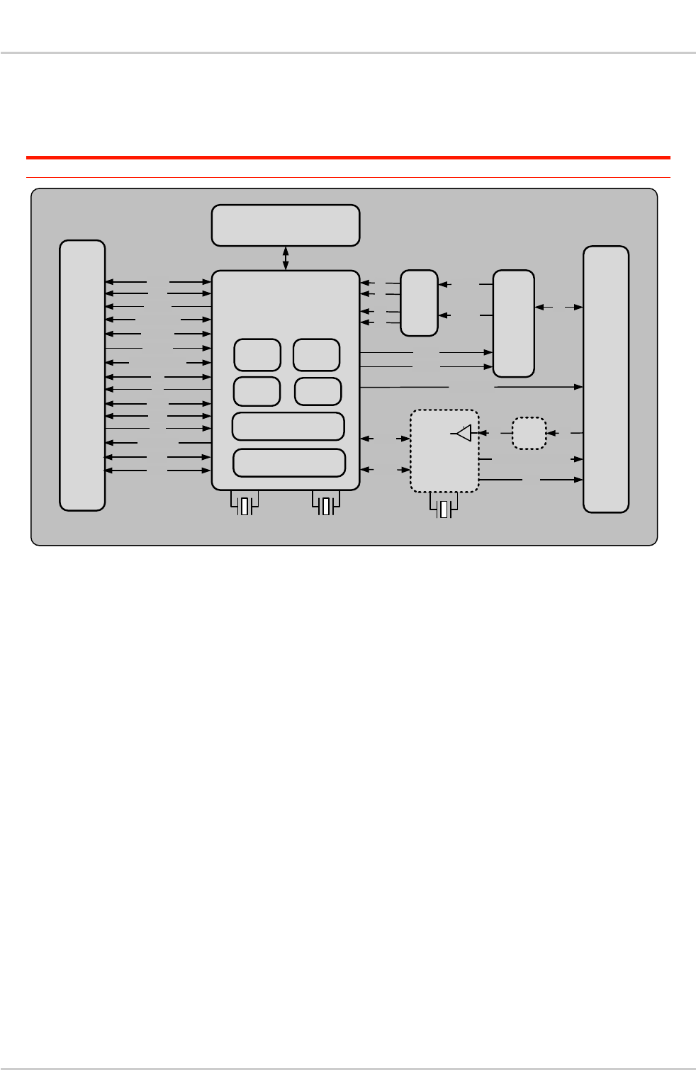
1.6. Architecture
The figure below presents an overview of the AirPrime HL6528x module internal architecture and
external interfaces.
Note: Dotted parts are only supported on the AirPrime HL6528-G and HL6528-G2.8V.
HL6528x
Memory
(Flash + RAM)
GNSS
SAW
Filters GSM
PA
&
Switch
CTRL
DATA
16.369MHz
26MHz 32.768KHz
UART1 (8pins)
SPI
VBAT
GND
VGPIO
VBAT_RTC
GPIO x8
ADC x2
I²C
MIC
SPEAKER
PCM
RF
RF
JTAG
LGA-
146
Baseband
EXT_LNA_GPS_EN
PPS
SAW
Filter
RF
LNA
SIM2
SIM1
MCU DSP
PMU RF
Analog Baseband
Peripherals
RX_HB
RX_LB
LB
LB
HB
HB
TX_LB
TX_HB
LGA-
146
2G_TX_ON
Figure 1. AirPrime HL6528x Architecture Overview
1.7. Interfaces
The AirPrime HL6528 and HL6528-2.8V modules provide the following interfaces and peripheral
connectivity:
1 8-pin UART
Active Low RESET
Active Low POWER-ON
1 1.8V/3V UIM
1 UIM 3V
1 Analog Audio Interface (Differential input/output)
1 Digital Audio
2 ADC
1 JTAG Interface
8 GPIOs with I²C multiplexes
2G TX Burst Indicator
GSM Antenna
Note: SPI interface is ONLY dedicated to SW traces debug.
4114016 Rev 3.0 January 28, 2014 14
Product Technical Specification
Introduction
In addition to the interfaces above, the AirPrime HL6528-G and HL6528-G2.8V modules also provide
the following interfaces and peripheral connectivity:
GPS Antenna
External LNA Enable/Disable
Pulse Per Second
1.8. Connection Interface
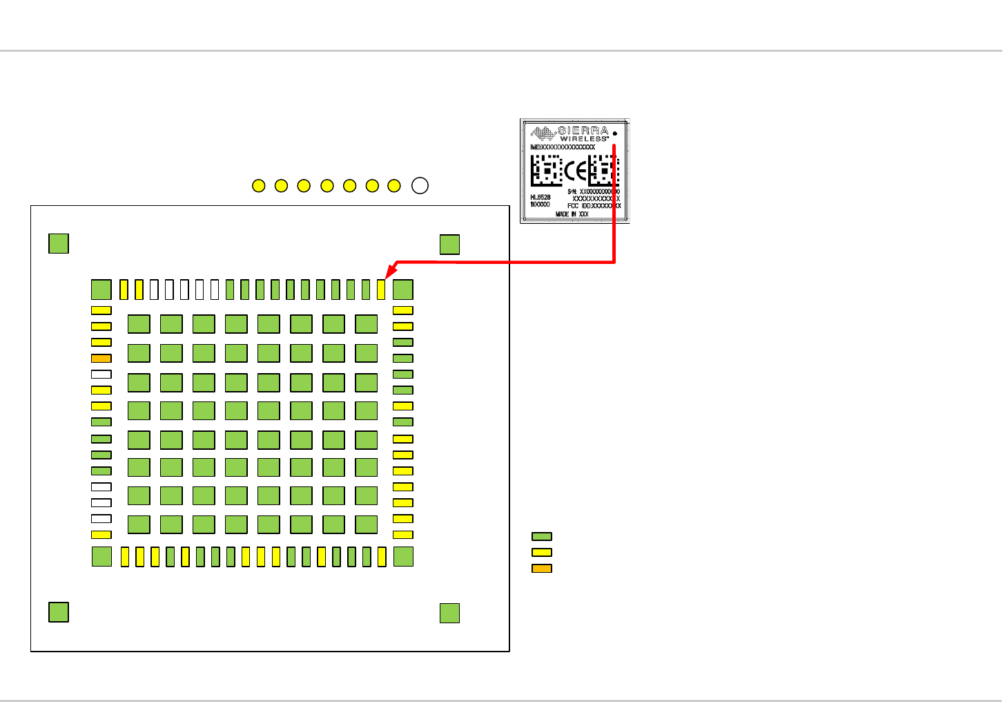
The AirPrime HL6528x module is an LGA form factor device. All electrical and mechanical
connections are made through the 146 pads Land Grid Array (LGA) on the bottom side PCB.
Figure 2. AirPrime HL6528x Module Mechanical Overview
The 146 pads have the following distribution
66 inner signal pads, 1x0.5mm, pitch 0.8mm
1 reference test point (Ground), 1.0mm diameter
7 test point (JTAG), 0.8mm diameter, 1.20mm pitch
64 inner ground pads, 1.0x1.0mm, pitch 1.825mm/1.475mm
4 inner corner ground pads, 1x1mm
4 outer corner ground pads, 1x0.9mm
1.9. ESD
According to IEC61000-4-2 model, the AirPrime HL6528x module can stand for:
+/-2kV ESD on all the LGA pins
+/-8kV ESD on RF pins
4114016 Rev 3.0 January 28, 2014 15
Product Technical Specification
Introduction
1.10. Environmental and Certifications
1.10.1. Environmental Specifications
The environmental specification for both operating and storage conditions are defined in the table
below.
Table 4. AirPrime HL6528x Module Environmental Specifications
Conditions
Range
Operating Class A
-30°C to +70°C
Operating Class B
-40°C to +85°C
Storage
-40°C to +90°C
Class A is defined as the operating temperature ranges that the device:
Shall exhibit normal function during and after environmental exposure.
Shall meet the minimum requirements of 3GPP or appropriate wireless standards.
Class B is defined as the operating temperature ranges that the device:
Shall remain fully functional during and after environmental exposure
Shall exhibit the ability to establish a voice, SMS or DATA call (emergency call) at all times
even when one or more environmental constraint exceeds the specified tolerance.
Unless otherwise stated, full performance should return to normal after the excessive
constraint(s) have been removed.
1.10.2. Regulatory
The AirPrime HL6528x module is compliant with the following regulations: R&TTE directive, GCF-CC,
CE marking, FCC, and PTCRB.
Table 5. Regulation Compliance
Document
Current
Version
Title
NAPRD.03
v5.10
(2012-01)
Overview of PCS Type certification review board (PTCRB) Mobile Equipment
Type Certification and IMEI control
GCF-CC
v3.45.1
(2012-03)
GCF Conformance Certification Criteria
TS 51.010-1
V10.0.0
(2012-03)
3rd Generation Partnership Project; Technical Specification Group GSM/EDGE
Radio Access Network; Digital cellular telecommunications system (Phase 2+);
Mobile Station (MS) conformance specification; Part 1: Conformance
specification
TS 51.010-2
V10.0.0
(2012-03)
3rd Generation Partnership Project; Technical Specification Group GSM/EDGE
Radio Access Network; Mobile Station (MS) conformance specification; Part 2:
Protocol Implementation Conformance Statement (PICS) proforma specification
4114016 Rev 3.0 January 28, 2014 16
Product Technical Specification
Introduction
Document
Current
Version
Title
EN 301511
V9.0.2
(2003-03)
Global System for Mobile Communications (GSM); Harmonized EN for Mobile
Stations in the GSM 900 and GSM 1800 Bands Covering Essential
Requirements Under Article 3.2 of the R&TTE Directive (1999/5/EC)
EN 301489-1
V1.9.2
(2011-09)
Electromagnetic compatibility and Radio spectrum Matters (ERM);
ElectroMagnetic Compatibility (EMC) standard for radio equipment and services;
Part 1: Common technical requirements
EN 301489-3
V1.4.1
(2002-08)
Electromagnetic compatibility and Radio spectrum Matters (ERM);
ElectroMagnetic Compatibility (EMC) standard for radio equipment and services;
Part 3: Specific conditions for Short-Range Devices (SRD) operating on
frequencies between 9 KHz and 40 GHz
EN 301489-7
V1.3.1
(2005-11)
Electromagnetic Compatibility and Radio Spectrum Matters (ERM);
ElectroMagnetic Compatibility (EMC) Standard for Radio Equipment and
Services; Part 7: Specific Conditions for Mobile and Portable Radio and Ancillary
Equipment of Digital Cellular Radio Telecommunications Systems (GSM and
DCS)
EN 60950-1
NA
IEC 60950-1:2005/A1:2009
EN 60950-1:2006/A11:2009/A1:2010/A12:2011
Information technology equipment – safety- and general requirements
EN 300440-1
v1.6.1
(2012-08)
Electromagnetic compatibility and Radio spectrum Matters (ERM); Short range
devices; Radio equipment to be used in the 1 GHz to 40 GHz frequency range;
Part 1: Technical characteristics and test methods
EN 300440-2
V1.4.1
(2012-08)
Electromagnetic compatibility and Radio spectrum Matters (ERM); Short range
devices; Radio equipment to be used in the 1 GHz to 40 GHz frequency range;
Part 2: Harmonized EN under article 3.2 of the R&TTE Directive
FCC Part 15B
NA
Subpart B - Radio frequency devices subpart B – Unintentional Radiators
FCC Part 22H
NA
Cellular Radiotelephone Service; Subpart H: Cellular Radiotelephone Service
FCC Part 24E
NA
Personal Communications Service; Subpart E: Broadband PCS.
RSS-132
Issue
2:2005
Cellular telephones employing new technologies operating in the 824-849 MHz
and 869-894 MHz bands.
RSS-133
Issue
5:2009
2 GHz personal communications services
AS/ACIF
S042.1
2008
Requirements for connection to an air interface of a telecommunications network
Part 1; General
AS/ACIF
S042.3
2005
Requirements for connection to an air interface of a Telecommunications
Network - Part 3: GSM Customer Equipment
AS/NZS
60950.1
2011
Safety of information technology equipment (IEC 60950-1, Ed.2.0: 2005, MOD)
SRRC
NA
State Radio Regulation Center - China Type Approval

4114016 Rev 3.0 January 28, 2014 17
Product Technical Specification
Introduction
1.10.3. RoHS Directive Compliant
The AirPrime HL6528x module is compliant with RoHS Directive 2011/65/EU which sets limits for the
use of certain restricted hazardous substances. This directive states that “from 1st July 2006, new
electrical and electronic equipment put on the market does not contain lead, mercury, cadmium,
hexavalent chromium, polybrominated biphenyls (PBB) or polybrominated diphenyl ethers (PBDE)”.
1.10.4. Disposing of the Product
This electronic product is subject to the EU Directive 2012/19/EU for Waste Electrical
and Electronic Equipment (WEEE). As such, this product must not be disposed of at a
municipal waste collection point. Please refer to local regulations for directions on
how to dispose of this product in an environmental friendly manner.
1.10.5. References
[1] AirPrime HL Series Customer Process Guidelines
Reference Number: 4114330
[2] AirPrime HL6 and HL8 Series AT Commands Interface Guide
Reference Number: 4114680
4114016 Rev 3.0 January 28, 2014 18
2. Pad Definition
AirPrime HL6528x module pins are divided into 3 functional categories.
Core functions and associated pins cover all the mandatory features for M2M connectivity and will be available by default across all CF3 family of
modules. These Core functions are always available and always at the same physical pin locations. A customer platform using only these functions
and associated pins is guaranteed to be forward and/or backward compatible with the next generation of CF3 modules.
Extension functions and associated pins bring additional capabilities to the customer. Whenever an Extension function is available on a module, it
is always at the same pin location.
Custom functions and associated pins are specific to a given module, and make an opportunistic use of specific chipset functions and I/Os.
Custom features should be used with caution as there is no guarantee that the custom functions available on a given module will be available on
other CF3 modules.
Other pins marked as “not connected” or “reserved” should not be used.
Table 6. Pad Description
Pin #
Signal Name
Function
I/O
Active
Low/ High
IO Voltage
Domain for
HL6528 and
HL6528-G
IO Voltage
Domain for
HL6528-2.8V
and HL6528-
G2.8V
Recommendation for
Unused Pins
Type
1
GPIO1/I2C1_CLK
General purpose
input/output/I2C Clock
I/O
1.8V
2.8V
Left Open
Extension
2
UART1_RI
UART1: Ring indicator
O
1.8V
2.8V
Left Open
Core
3
UART1_RTS
UART1: Request to send
I
L
1.8V
2.8V
Connect to UART1_CTS
Core
4
UART1_CTS
UART1: Clear to send
O
L
1.8V
2.8V
Connect to UART1_RTS
Core
5
UART1_TX
UART1: Transmit data
I
1.8V
2.8V
Mandatory connection
Core
6
UART1_RX
UART1: Receive data
O
1.8V
2.8V
Mandatory connection
Core
7
UART1_DTR
UART1: Data terminal ready
I
L
1.8V
2.8V
Connect to UART1_DSR
Core
8
UART1_DCD
UART1: Data carrier detect
O
L
1.8V
2.8V
Left Open
Core

4114016 Rev 3.0 January 28, 2014 19
Product Technical Specification
Pad Definition
Pin #
Signal Name
Function
I/O
Active
Low/ High
IO Voltage
Domain for
HL6528 and
HL6528-G
IO Voltage
Domain for
HL6528-2.8V
and HL6528-
G2.8V
Recommendation for
Unused Pins
Type
9
UART1_DSR
UART1: Data set ready
O
L
1.8V
2.8V
Connect to UART1_DTR
Core
10
GPIO2/UIM2_VCC_CT
RL
General purpose
input/output (
UIM2 VCC Control
I/O
1.8V
2.8V
Left Open
Core
11
RESET_IN
Input reset signal
I
L
1.8V
2.8V
Left Open (Test point
recommended)
Core
12
NC
Not Connected
Not Connected
13
NC
Not Connected
Not Connected
14
NC
Not Connected
Not Connected
15
NC
Not Connected
Not Connected
16
NC
Not Connected
Not Connected
17
SPKR_N
Speaker negative output
(32Ω impedance)
O
2.8V
2.8V
Left Open
Extension
18
SPKR_P
Speaker positive output
(32Ω impedance)
O
2.8V
2.8V
Left Open
Extension
19
MIC_P
Microphone positive input
I
2.8V
2.8V
Left Open
Extension
20
MIC_N
Microphone negative input
I
2.8V
2.8V
Left Open
Extension
21
BAT_RTC
Power supply for RTC
backup
I/O
3.0V
3.0V
C=10µF
Extension
22
TP2
Factory use only
I
L
1.8V
2.8V
Mandatory Left Open
Custom
23
NC
Not Connected
Not Connected
24
ADC1
Analog to digital conversion
I
2.8V
2.8V
Connected to Ground
Extension
25
ADC0
Analog to digital conversion
I
2.8V
2.8V
Connected to Ground
Extension
26
UIM1_VCC
1.8V/3V UIM1 Power supply
O
1.8V/3V
1.8V/3V
Mandatory connection
Core
4114016 Rev 3.0 January 28, 2014 20
Product Technical Specification
Pad Definition
Pin #
Signal Name
Function
I/O
Active
Low/ High
IO Voltage
Domain for
HL6528 and
HL6528-G
IO Voltage
Domain for
HL6528-2.8V
and HL6528-
G2.8V
Recommendation for
Unused Pins
Type
27
UIM1_CLK
1.8V/3V UIM1 Clock
O
1.8V/3V
1.8V/3V
Mandatory connection
Core
28
UIM1_DATA
1.8V/3V UIM1 Data
I/O
1.8V/3V
1.8V/3V
Mandatory connection
Core
29
UIM1_RESET
1.8V/3V UIM1 Reset
O
L
1.8V/3V
1.8V/3V
Mandatory connection
Core
30
NC
NC (Reserved for 3G
compatibility)
Not Connected
31
NC
NC (Reserved for 3G
compatibility)
Not Connected
32
NC
NC (Reserved for 3G
compatibility)
Not Connected
33
PCM_OUT
PCM data out
O
2.8V
2.8V
Left Open
Extension
34
PCM_IN
PCM data in
I
2.8V
2.8V
Left Open
Extension
35
PCM_SYNC
PCM sync out
I/O
2.8V
2.8V
Left Open
Extension
36
PCM_CLK
PCM clock
I/O
2.8V
2.8V
Left Open
Extension
37
GND
Ground
GND
0V
0V
Mandatory connection
Core
38
RF_GPS*
RF GPS Input
I
Mandatory connection
Extension
39
GND
Ground
GND
0V
0V
Mandatory connection
Core
40
GPIO7
General purpose
input/output
I/O
1.8V
2.8V
Left Open
Core
41
GPIO8
General purpose
input/output
I/O
1.8V
2.8V
Left Open
Core
42
PPS*
GPS Pulse Per Second
O
1.8V
2.8V
Left Open
Extension
43
EXT_LNA_GPS_EN*
External GPS LNA enable
O
H
1.8V
2.8V
Left Open
Extension
44
SPI1_SRDY
Debug use only
SPI Slave Ready
I
1.8V
2.8V
Left Open (Test point
mandatory)
Extension
45
VGPIO
GPIO voltage output
O
1.8V
2.8V
Left Open
Core
4114016 Rev 3.0 January 28, 2014 21
Product Technical Specification
Pad Definition
Pin #
Signal Name
Function
I/O
Active
Low/ High
IO Voltage
Domain for
HL6528 and
HL6528-G
IO Voltage
Domain for
HL6528-2.8V
and HL6528-
G2.8V
Recommendation for
Unused Pins
Type
46
GPIO6
General purpose
input/output
I/O
1.8V
2.8V
Left Open
Core
47
TP1
Test Point 1
0- JTAG Enable
Open-Normal Mode
I
L
1.8V
2.8V
Left Open
Extension
48
GND
Ground
GND
0V
0V
Mandatory connection
Core
49
RF_MAIN
RF GSM Input/output
I/O
Mandatory connection
Core
50
GND
Ground
GND
0V
0V
Mandatory connection
Core
51
SPI1_MRDY
Debug use only
SPI Master Ready
O
1.8V
2.8V
Left Open (Test point
mandatory)
Extension
52
SPI1_MISO
Debug use only
SPI Master In Slave Out
I
1.8V
2.8V
Left Open (Test point
mandatory)
Extension
53
SPI1_CLK
Debug use only
SPI Clock
O
1.8V
2.8V
Left Open (Test point
mandatory)
Extension
54
SPI1_MOSI
Debug use only
SPI Master Out Slave In
O
1.8V
2.8V
Left Open (Test point
mandatory)
Extension
55
UIM2_VCC
UIM2 Power supply
O
2.8V
2.8V
Left Open
Extension
56
UIM2_DATA
UIM2 Data
I/O
2.8V
2.8V
Left Open
Extension
57
UIM2_RESET/BUZZER
UIM2 Reset/Buzzer
O
2.8V
2.8V
Left Open
Extension
58
UIM2_CLK/PWM
UIM2 Clock/PWM
O
2.8V
2.8V
Left Open
Extension
59
PWR_ON
Active Low Power On
control signal
I/O
L
3.0V
3.0V
Mandatory connection
Core
60
2G_TX_ON
2G TX burst indicator
O
H
2.8V
2.8V
Left Open
Extension
61
VBATT_PA
3.7V Power Amplifier Power
supply
I
3.7V
3.7V
Mandatory connection
Core
4114016 Rev 3.0 January 28, 2014 22
Product Technical Specification
Pad Definition
Pin #
Signal Name
Function
I/O
Active
Low/ High
IO Voltage
Domain for
HL6528 and
HL6528-G
IO Voltage
Domain for
HL6528-2.8V
and HL6528-
G2.8V
Recommendation for
Unused Pins
Type
62
VBATT_PA
3.7V Power Amplifier Power
supply
I
3.7V
3.7V
Mandatory connection
Core
63
VBATT
3.7V Power supply
I
3.7V
3.7V
Mandatory connection
Core
64
UIM1_DET/GPIO3
UIM1 Detection/General
purpose input/output
I/O
H
1.8V
2.8V
Left Open
Core
65
UIM2_DET/GPIO4
UIM2 Detection/General
purpose input/output
I/O
H
1.8V
2.8V
Left Open
Extension
66
GPIO5/I2C1_DATA
General purpose
input/output/I²C DATA
I/O
1.8V
2.8V
Left Open
Extension
67-70
GND
Ground
GND
0V
0V
Mandatory connection
Core
71-
166
Note: These pins are not available on the AirPrime HL6548x modules
167-
234
GND
GND
GND
0V
0V
Mandatory connection
Core
235
TEST_PIN
Ground (Test Point)
GND
0V
0V
Left Open
Not connected
236
JTAG_RESET
JTAG RESET
I
L
1.8V
2.8V
Left Open
Extension
237
JTAG_TCK
JTAG Test Clock
I
1.8V
2.8V
Left Open
Extension
238
JTAG_TDO
JTAG Test Data Output
O
1.8V
2.8V
Left Open
Extension
239
JTAG_TMS
JTAG Test Mode Select
I
1.8V
2.8V
Left Open
Extension
240
JTAG_TRST
JTAG Test Reset
I
L
1.8V
2.8V
Left Open
Extension
241
JTAG_TDI
JTAG Test Data Input
I
1.8V
2.8V
Left Open
Extension
242
JTAG_RTCK
JTAG Returned Test Clock
O
1.8V
2.8V
Left Open
Extension
* This pin is only available on the HL6528-G and H6528-G2.8V.
4114016 Rev 3.0 January 28, 2014 23
Product Technical Specification
Pad Definition
2.1.1. Pin Configuration (Top View)
168
169
167
170
18
17
16
15
14
13
12
11
10
9
8
7
6
4
3
2
1
5
66
65
64
63
62
61
60
59
34
35
36
37
38
39
40
41
42
43
44
45
46
48
49
50
51
47
58
57
56
55
53
52
54
70
67
19
20
21
22
23
24
25
26
27
28
29
30
32
33
31
69
68
192 193 194 195 196 197 198 171
191 214 215 216 217 218 199 172
190 213 228 229 230 219 200 173
189 212 227 234 231 220 201 174
188 211 226 233 232 221 202 175
187 210 225 224 223 222 203 176
186 209 208 207 206 205 204 177
185 184 183 182 181 180 179 178
235
236237238239240241242
GND
GPIO5/I2C1_DATA
UIM2_DET/GPIO4
UIM1_DET/GPIO3
VBATT
VBATT_PA
VBATT_PA
2G_TX_ON
PWR_ON
UIM2_CLK/PWM
UIM2_RESET/BUZZER
UIM2_DATA
UIM2_VCC
SPI1_MOSI
SPI1_CLK
SPI1_MISO
GND
GND
MIC_P
MIC_N
BAT_RTC
RESERVED
NC
ADC1
ADC0
UIM1_VCC
UIM1_CLK
UIM1_DATA
UIM1_RESET
NC
NC
NC
PCM_OUT
GND
PCM_IN
PCM_SYNC
PCM_CLK
GND
RF_GPS
GND
GPIO7
GPIO8
PPS
EXT_LNA_GPS_EN
SPI1_SRDY
VGPIO
GPIO6
TP1
GND
RF_MAIN
GND
SPI1_MRDY
SPKR_P
SPKR_N
NC
NC
NC
NC
NC
RESET_IN
GPIO2
UART1_DSR
UART1_DCD
UART1_DTR
UART1_RX
UART1_TX
UART1_CTS
UART1_RTS
UART1_RI
GPIO1/I2C1_CLK
JTAG_RTCK
JTAG_TDI
JTAG_TRST
JTAG_TMS
JTAG_TDO
JTAG_TCK
JTAG_RESET
TEST POINT
Core pin
Extension pin
Custom pin
Figure 3. Pin Configuration
4114016 Rev 3.0 January 28, 2014 24
3. Detailed Interface Specifications
Note: If not specified, all electrical values are given for VBATT=3.7V and an operating temperature of
25°C.
For standard applications, VBATT and VBATT_PA must be tied externally to the same power
supply. For some specific applications, AirPrime HL6528x module supports separate VBATT and
VBATT_PA connection if requirements below are fulfilled.
3.1. Power Supply
The AirPrime HL6528x module is supplied through the VBATT signal with the following characteristics.
Table 7. Power Supply
Minimum
Typical
Maximum
VBATT voltage (V)
3.21
3.7
4.5
VBATT_PA voltage (V) Full Specification
3.01
3.7
4.5
VBATT_PA voltage (V) Extended Range2
2.82
3.7
4.5
1 This value has to be guaranteed during the burst
2 No guarantee of 3GPP performances over extended range
3.2. Current Consumption
The following table lists the current consumption of the AirPrime HL6528x module at different
conditions.
Note: Typical values are defined for VBATT/VBATT_PA at 3.7V, for a 50ohms impedance at all RF ports.
Max values are provided for a VSWR 3:1.
Table 8. Current Consumption
Parameters
Min.
Typ.
Max.
Off mode (HL6528 and HL6528-2.8V) (µA)
TBD
40
TBD
Off mode (HL6528-G and HL6528-G2.8V) (µA)
TBD
40
TBD
GSM Sleep mode (mA)
Single UIM operation
DRX2
1.3
1.4
2.5
DRX5
0.9
1.1
2.2
DRX9
0.8
1.0
2.0
GSM Sleep mode (mA)
Dual UIM operation
DRX2
3.0
3.1
4.5
DRX5
1.8
2.0
3.1
DRX9
1.5
1.7
2.6
GSM in communication mode (mA)
GSM900 / GSM850
(PCL=5)
TBD
220
TBD
DCS / PCS (PCL=0)
TBD
160
TBD
GPRS (2 TX, 3 RX) (mA)
GSM900 / GSM850
(PCL=5)
TBD
380
TBD
DCS / PCS (PCL=0)
TBD
270
TBD
4114016 Rev 3.0 January 28, 2014 25
Product Technical Specification
Detailed Interface Specifications
Parameters
Min.
Typ.
Max.
Peak Current consumption (A)
GSM900 / GSM850
TBD
1.50
TBD
DCS / PCS
TBD
0.90
TBD
GNSS Acquisition1 (mA)
GSM registered on network
Max value3
43
51
64
Min value4
TBD
28
TBD
GNSS Navigation (1Hz)1 (mA)
GSM registered on network
Max value3
39
45
57
Min value4
TBD
25
TBD
GNSS Navigation (1Hz)1 (mA)
GSM in Flight mode
Max value3
TBD
TBD
Min value4
TBD
TBD
GNSS Hibernate mode2 (mA)
GSM registered on network
Max value3
18
20
26
Min value4
TBD
1.5
TBD
1 Maximum SVs in view, signal level @-130dBm, high gain configuration
2 Hot start conditions are maintained in Hibernate mode3 Baseband is running (or no sleep mode allowed) in max value
condition. Refer to document [2] AirPrime HL6 and HL8 Series AT Commands Interface Guide for sleep mode
description.
4 Baseband is in sleep mode in min value condition. Refer to document [2] AirPrime HL6 and HL8 Series AT
Commands Interface Guide for sleep mode description.
Table 9. Current Consumption per power supply VBATT / VBATT_PA
Parameters
Min.
Typ.
Max.
VBATT_PA
Peak current (A)
GSM communication
mode, 2TX
GSM900 / GSM850 (PCL=5)
DCS / PCS (PCL=0)
Peak current (A)
GSM communication
mode, 1TX
GSM900 / GSM850 (PCL=5)
1.30
DCS / PCS (PCL=0)
0.80
Average current (mA)
GSM communication
mode, 1TX
GSM900 / GSM850 (PCL=5)
150
DCS / PCS (PCL=0)
90
VBATT
(HL6528 and
HL6528-2.8V)
Peak current (A)
GSM communication
mode, 2TX
GSM900 / GSM850 (PCL=5)
DCS / PCS (PCL=0)
Peak current (A)
GSM communication
mode, 1TX
GSM900 / GSM850 (PCL=5)
290
DCS / PCS (PCL=0)
125
Average current (mA)
GSM communication
mode, 1TX
GSM900 / GSM850 (PCL=5)
70
DCS / PCS (PCL=0)
70
VBATT
(HL6528-G and
HL6528-G2.8V)
Peak current (A)
GSM communication
mode, 2TX
GNSS Navigation
mode
GSM900 / GSM850 (PCL=5)
DCS / PCS (PCL=0)
Peak current (A)
GSM communication
mode, 1TX
GNSS Navigation
mode
GSM900 / GSM850 (PCL=5)
DCS / PCS (PCL=0)
4114016 Rev 3.0 January 28, 2014 26
Product Technical Specification
Detailed Interface Specifications
Parameters
Min.
Typ.
Max.
Average current (mA)
GSM communication
mode, 1TX
GNSS Navigation
mode
GSM900 / GSM850 (PCL=5)
DCS / PCS (PCL=0)
3.3. VGPIO
The VGPIO output can be used to:
Pull-up signals such as I/Os
Supply the digital transistors driving LEDs
Act as a voltage reference for the ADC interfaces, ADC0 and ADC1
The VGPIO output is available when the AirPrime HL6528x module is switched ON.
Table 10. VGPIO Electrical Characteristics
Parameter
HL6528, HL6528G
HL6528-2.8V, HL6528-G2.8V
Remarks
Min
Typ
Max
Min
Typ
Max
Voltage level (V)
1.70
1.80
1.90
2.65
2.80
2.95
Both active mode and
sleep mode
Current capability
active mode (mA)
-
-
50
-
-
50
Current capability
sleep mode (mA)
-
-
3
-
-
3
32KHz system clock
enable
Line regulation
(mV/V)
-
-
50
-
-
50
Iout = MAX
Rise Time(ns)
-
-
6
-
-
6
Test load capacitor =
30 pF
4114016 Rev 3.0 January 28, 2014 27
Product Technical Specification
Detailed Interface Specifications
3.4. BAT_RTC
The AirPrime HL6528x module provides an input/output to connect a Real Time Clock power supply.
This pin is used as a back-up power supply for the internal Real Time Clock. The RTC is supported
when VBATT is available but a back-up power supply is needed to save date and hour when VBATT
is switched off.
If VBATT is available, the back-up battery can be charged by the internal 3.0V power supply regulator.
Table 11. BAT_RTC Electrical Characteristics
Parameter
Minimum
Typical
Maximum
Input voltage (V)
-
3.0
-
Input current consumption (µA)
-
2.5
-
Output voltage (V)
2.82
3.0
3.18
Max charging current (@VBATT=3.6V) (mA)
-
0.6
-
3.5. UIM Interface
The AirPrime HL6528x module has two physical UIM interfaces – one main UIM interface (UIM1), and
a second UIM interface (UIM2) reserved for Dual UIM Dual Standby option.
3.5.1. UIM1 Interface
The UIM1 interface allows control of a 1.8V/3V UIM and is fully compliant with GSM 11.11
recommendations related to UIM functions.
The five signals used by this interface are as follows:
UIM1_VCC: power supply
UIM1_CLK: clock
UIM1_IO: I/O port
UIM1_RST: reset
UIM1_DET: UIM detection (optional)
Table 12. Electrical Characteristics of UIM1
Parameter
Minimum
Typical
Maximum
Remarks
UIM1 Interface Voltage (V)
(VCC,CLK,IO,RST)
2.7
3.0
3.15
The appropriate output
voltage is auto detected and
selected by software.
1.65
1.80
1.95
UIM1_VCC Current (mA)
-
-
10
Max output current in sleep
mode = 3 mA
UIM1_VCC Line Regulation (mV/V)
-
-
50
At Iout_Max
UIM1_VCC Power-up Setting Time
(us) from power down
-
10
-
4114016 Rev 3.0 January 28, 2014 28
Product Technical Specification
Detailed Interface Specifications
3.5.1.1. UIM1_DET
UIM1_DET is used to detect and notify the application about the insertion and removal of a UIM
device in the UIM socket connected to the main UIM interface (UIM1). When a UIM is inserted, the
state of UIM1_DET transitions from logic 0 to logic 1. Inversely, when a UIM is removed, the state of
UIM1_DET transitions from logic 1 to logic 0.
The GPIO for UIM1_DET is GPIO3..
3.5.2. UIM2 Interface
The UIM2 interface is optional and only intended to be used with Dual UIM Dual Standby feature.
Note: This is the preferred interface for when MFF2 UIM cards are used.
The five signals used by this interface are as follows:
UIM2_VCC: power supply
UIM2_CLK: clock
UIM2_IO: I/O port
UIM2_RST: reset
UIM2_DET: HW detection (optional)
UIM2_VCC_CTRL: control signal for external analog switch (mandatory)
Table 13. Electrical Characteristics of UIM2
Parameter
Minimum
Typical
Maximum
Remarks
UIM2 Interface Voltage (V)
(VCC, CLK, IO, RST)
2.7
2.85
3.0
UIM2 Interface Voltage (V)
(VCC_CTRL)
1.8 or 2.8
UIM2_VCC_CTRL is on
VGPIO power domain
UIM2_VCC Current (mA)
-
-
10
Max output current in sleep
mode = 3 mA
Note: The UIM2 interface is fixed at 3V; do not use a direct connection with a 1.8V-only UIM card.
3.5.2.1. UIM2_DET
UIM2_DET is used to detect and notify the application about the insertion and removal of a UIM
device in the UIM socket connected to the second UIM interface (UIM2). When a UIM is inserted, the
state of UIM2_DET transitions from logic 0 to logic 1. Inversely, when a UIM is removed, the state of
UIM2_DET transitions from logic 1 to logic 0.
The GPIO for UIM2_DET is GPIO4..
3.5.2.2. UIM2_VCC_CTRL
An analog switch must be added on the customer board when using the UIM2 interface. This analog
switch is controlled by GPIO2.
4114016 Rev 3.0 January 28, 2014 29
Product Technical Specification
Detailed Interface Specifications
Table 14. UIM2_VCC_CTRL Analog Switch Truth Table
GPIO2 (UIM2_VCC_CTRL)
Function
Low
UIM2_VCC connected to UIM2_VCC
High
UIM2_VCC disconnected from UIM2_VCC
HL6528x
SIM2 Card
Analog
Switch
GPIO2 (UIM2_VCC_CTRL)
UIM2_VCC
UIM2_RESET
UIM2_CLK
UIM2_DATA
SIM2_VCC
SIM2_RST
SIM2_CLK
SIM2_DATA
UIM2_DET (GPIO) SIM2_DET
Figure 4. UIM2 with an Analog Switch
3.6. Electrical Information for Digital I/O
The table below enumerates the electrical characteristics of the following digital interfaces:
UART
PCM
GPIOs
I²C
SPI
JTAG
RESET
Depending on the AirPrime HL6528x module variant, digital IOs are either 2.8V or 1.8V power
domain.
Note: The PCM interface only supports 2.8V even with 1.8V configuration.
Table 15. Digital I/O Electrical Characteristics
Parameter
HL6528, HL6528G
HL6528-2.8V,
HL6528-G2.8V
Remarks
Min
Typ
Max
Min
Typ
Max
Input Current-High(µA)
-10
-
10
-10
-
10
Input Current-Low(µA)
-10
-
10
-10
-
10
DC Output Current-
High(mA)*
-
-
15
-
-
15
Pin driving a "1" with
output set at "0"
4114016 Rev 3.0 January 28, 2014 30
Product Technical Specification
Detailed Interface Specifications
Parameter
HL6528, HL6528G
HL6528-2.8V,
HL6528-G2.8V
Remarks
Min
Typ
Max
Min
Typ
Max
DC Output Current-
Low(mA)*
-15
-
-
-15
-
-
Pin driving a "0" with
output set at "1"
Input Voltage-High(V)
1.4
2.2
2.4
3.2
Input Voltage-Low(V)
-0.2
-
0.4
-0.2
-
0.4
Output Voltage-High(V)
1.7
-
1.9
2.7
-
2.95
Output Voltage-Low(V)
0
-
0.1
0
-
0.1
* The maximum current for one GPIO is 15mA, but all GPIOs can’t provide 15mA at a time since the VIO is
limited to 50mA
3.7. Main Serial Link (UART1)
The main serial link (UART1) is used for communication between the AirPrime HL6528x module and
a PC or host processor. It consists of a flexible 8-wire serial interface that complies with RS-232
interface.
The supported baud rates of the UART1 are 1200, 2400, 4800, 9600, 19200, 38400, 57600 and
115200 bit/s, with autobauding and up to 1Mbit/s at maximum baud rate.
The signals used by UART1 are as follows:
TX data (UART1_TX)
RX data (UART1_RX)
Request To Send (UART1_RTS)
Clear To Send (UART1_CTS)
Data Terminal Ready (UART1_DTR)
Data Set Ready (UART1_DSR)
Data Carrier Detect (UART1_DCD)
Ring Indicator (UART1_RI)
UART1 pin description is summarized below.
Table 16. UART1 Pin Description
Signal Name (Module side)
I/O (Module side)
Description
UART1_DTR
I (active low)
Prevents the AirPrime HL6528x from entering sleep
mode, switches between data mode and command
mode, and wakes the module up.
UART1_DCD
O
Signal data connection in progress
UART1_RX
O
Receive data
UART1_RTS
I
Wakes the module up when KSLEEP=1 is used
UART1_TX
I
Transmit data
UART1_CTS
O
AirPrime HL6528x is ready to receive AT commands
UART1_RI
O
Signal incoming calls (voice and data), SMS, etc.
UART1_DSR
O
Signal UART interface is ON
4114016 Rev 3.0 January 28, 2014 31
Product Technical Specification
Detailed Interface Specifications
3.8. Power On Signal (PWR_ON)
A low level signal has to be provided to switch the AirPrime HL6528x module ON.
It is internally connected to the permanent 3.0V supply regulator inside the HL6528x via a pull-up
resistor. Once VBATT is supplied to the HL6528x module, this 3.0V supply regulator will be enabled
and so PWR_ON signal is by default at high level.
The PWR_ON signal’s characteristics are listed in the table below.
Table 17. PWR_ON Electrical Characteristics
Parameter
Minimum
Typical
Maximum
Input Voltage-Low (V)
-
0.4
Input Voltage-High (V)
2.4
-
3.3
Power-up period (ms) from PWR_ON falling edge
2000
-
-
Note: As PWR_ON is internally pulled up, a simple open collector or open drain transistor must be used
for ignition.
The PWR_ON signal will become low after the module is ready. It cannot be directly driven by a
GPIO signal.
VGPIO is an output from the module that can be used to check if the module is active.
When VGPIO = 0V the module is OFF.
When VGPIO = 2.8V or 1.8V the module is ON (it can be in Idle, Communication or Sleep
mode)
After a few seconds, the UART1_CTS enters active state and the module is ready to receive AT
commands.
Figure 5. PWR_ON Sequence
Note: PWR_ON cannot be used to power the module off. The module is powered off with AT command
“AT*PSCPOF”.
4114016 Rev 3.0 January 28, 2014 32
Product Technical Specification
Detailed Interface Specifications
3.9. Reset Signal (RESET)
To reset the module, a low level pulse must be sent on RESET pin for at least 10ms. This action will
immediately restart the AirPrime HL6528x module. It is therefore useless to perform a new ignition
sequence (PWR_ON) afterwards.
As RESET is internally pulled up, a simple open collector or open drain transistor can be used to
control it.
The RESET signal will reset the registers of the CPU and reset the RAM memory as well.
Note: As RESET is referenced to the VGPIO domain (internally to the module) it is impossible to reset
before the module starts or to try to use the RESET as a way to start the module.
Parameter
HL6528, HL6528G
HL6528-2.8V, HL6528-G2.8V
Min
Typ
Max
Min
Typ
Max
Input Voltage-Low (V)
-
0.4
-
0.4
Input Voltage-High (V)
1.4
-
2.4
-
Power up Period (ms) from RESET
falling edge
38
-
-
38
-
-
3.10. ADC
Two Analog to Digital Converter input, ADC0 and ADC1 are provided by the AirPrime HL6528x
module. These converters are 10-bit resolution ADCs ranging from 0 to 3V.
Typically, the ADCx input can be used to monitor external temperature. This is very useful for
monitoring the application temperature and can be used as an indicator to safely power OFF the
application in case of overheating (for Li-Ion batteries).
Both ADCs have the characteristics listed in the table below.
Table 18. ADC Electrical Characteristics
Parameter
Minimum
Typical
Maximum
Remarks
ADC Resolution (bits)
-
10
-
Input Voltage Range (V)
0
-
3
General purpose input
Update rate per channel (KHz)
-
-
200
Differential Nonlinearity (bits)
-1
-
+3
Integral Nonlinearity (bits)
-2.5
-
+2.5
LSB
Offset Error (mV)
-
5
-
Gain Error (mV/LSB)
-
0.02
-
Input Resistance (kΩ)
120
150
-
Input Capacitance (pF)
-
-
10
3.11. Analog Audio Interfaces
The AirPrime HL6528x module supports one differential microphone input and one differential
speaker output. It also includes a noise suppression and echo cancellation feature which allows for an
enhanced voice call quality.
4114016 Rev 3.0 January 28, 2014 33
Product Technical Specification
Detailed Interface Specifications
3.11.1. Analog Audio Input
The microphone input can either have a single-ended or a differential connection. However,
performance with common mode noise and TDMA noise varies depending on the connection mode
and PCB layout.
When connecting a microphone to the AirPrime HL6528x module, ensure to have a very good ground
plane, very good filtering as well as shielding in order to avoid any disturbance on the audio path.
The gain of the microphone input can be tuned using AT commands.
The AirPrime HL6528x module microphone pins already include suitable biasing for an electret
microphone. The electret microphone can then be connected directly on the inputs for easy
connection.
AC coupling is also already embedded in the HL6528x embedded module.
Table 19. Analog Audio Interface Input
Parameter
Minimum
Typical
Maximum
Test Conditions
MIC_P DC Biasing (V)
2.4
Through internal 2.2kΩ
MIC_N DC Biasing (V)
0
Through internal 2.2kΩ
Maximum input range (V)
1.4
Gain = - 6dB
Nominal reference level (mVrms)
16
Gain = + 34dB
Input Micro amplifier gain (dB)
-6
+ 50
Note: It is recommended to add ESD protection to the microphone when it is exposed to the external
environment. The ESD protection should be connected between the audio lines and a good ground,
and placed as close to the microphone as possible.
3.11.2. Analog Audio Outputs
Table 20. Analog Audio Interface Output
Parameter
Min
Typ
Max
Test Conditions
Maximum output range (Vrms)
1.65
Load=32Ω, THD=1%, Output gain = 8 dB
Load resistance (Ω)
32
Output amplifier gain (dB)
-28
-
8
Note: It is recommended to add ESD protection to the speaker when it is exposed to the external
environment. The ESD protection should be connected between the audio lines and a good ground,
and placed as close to the speaker as possible.
It’s important to select an appropriate speaker. The following enumerates the recommended speaker
characteristics.
Table 21. Recommended Speaker Characteristics
Characteristic
Value
Input power: rated / max
0.1W (Rate)
Audio chain impedance
32Ω +/- 10% at 1V 1KHz
Frequency Range
300 Hz ~ 4.0 KHz
4114016 Rev 3.0 January 28, 2014 34
Product Technical Specification
Detailed Interface Specifications
Characteristic
Value
Sensitivity (S.P.L)
>105 dB at 1KHz with IEC318 coupler
Distortion
5% max at 1K Hz, nominal input power
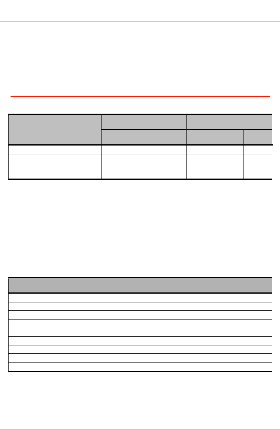
3.12. PCM
The Digital Audio Interface (PCM) interface allows connectivity with standard audio peripherals. It can
be used, for example, to connect an external audio codec.
The programmability of this interface allows addressing a large range of audio peripherals.
The signals used by the Digital Audio Interface are as follows:
PCM_SYNC: The frame synchronization signal delivers an 8KHz frequency pulse that
synchronizes the frame “data in” and the frame “data out” (short frame synchronization only).
PCM_CLK: The frame bit clock signal controls data transfer with the audio peripheral.
PCM_OUT: The frame “data out” relies on the selected configuration mode.
PCM_IN: The frame “data in” relies on the selected configuration mode.
The PCM interface is a high speed full duplex interface that can be used to send and receive digital
audio data to external audio ICs. The digital audio interface also features the following:
PCM master or slave mode
8 bits or 16 bits data word length
MSB or LSB first
Rising or falling sampling clock edge
Configurable PCM bit clock rate up to 1MHz
Refer to the following table for the electrical characteristics of the digital audio interface.
Table 22. Digital Audio Interface Electrical Characteristics
Signal
Description
Minimum
Typical
Maximum
Tsync_low + Tsync_high
PCM-SYNC period (µs)
125
Tsync_low
PCM-SYNC low time (µs)
124
Tsync_high
PCM-SYNC high time (µs)
1
TSYNC-CLK
PCM-SYNC to PCM-CLK time (ns)
651
TCLK-cycle
PCM-CLK period (ns)
1302
TIN-setup
PCM-IN setup time (ns)
50
TIN-hold
PCM-IN hold time (ns)
50
TOUT-delay
PCM-OUT delay time (ns)
20
TSYNC-delay
PCM-SYNC output delay (ns)
-11
9
The following figure shows the PCM timing waveform.
4114016 Rev 3.0 January 28, 2014 35
Product Technical Specification
Detailed Interface Specifications
Figure 6. PCM Timing Waveform
3.13. I2C Interface
NMEA frames can be output from the UART or through a dedicated serial port (I2C).
Table 23. I2C Pin Description
Pad #
Name
Function
1
I2C1_CLK
I2C Serial Clock Line
66
I2C1_DATA
I2C Serial Data Line
Note: I2C pins are multiplexed with GPIO features.
The main characteristics of the I2C interface are as follows:
Master mode (I2C1_CLK is an output of the AirPrime HL6528x module)
I2C clock is set at 400KHz
As AirPrime HL6528x module is master only, devices connected to the I2C bus shall be slave
devices. In order for AirPrime HL6528x module to communicate with the slave device, the
slave 7-bit address shall be loaded inside the module before activating the GPS NMEA output.
See [2] for AT command description.
3.14. Debug Interfaces
The AirPrime HL6528x module provides two interfaces for a powerful debug system.
3.14.1. SW Traces
The AirPrime HL6528x module provides a SW TRACE interface, providing real-time instruction and
data trace of the modem core. The SW TRACE interface is accessible through the SPI port.
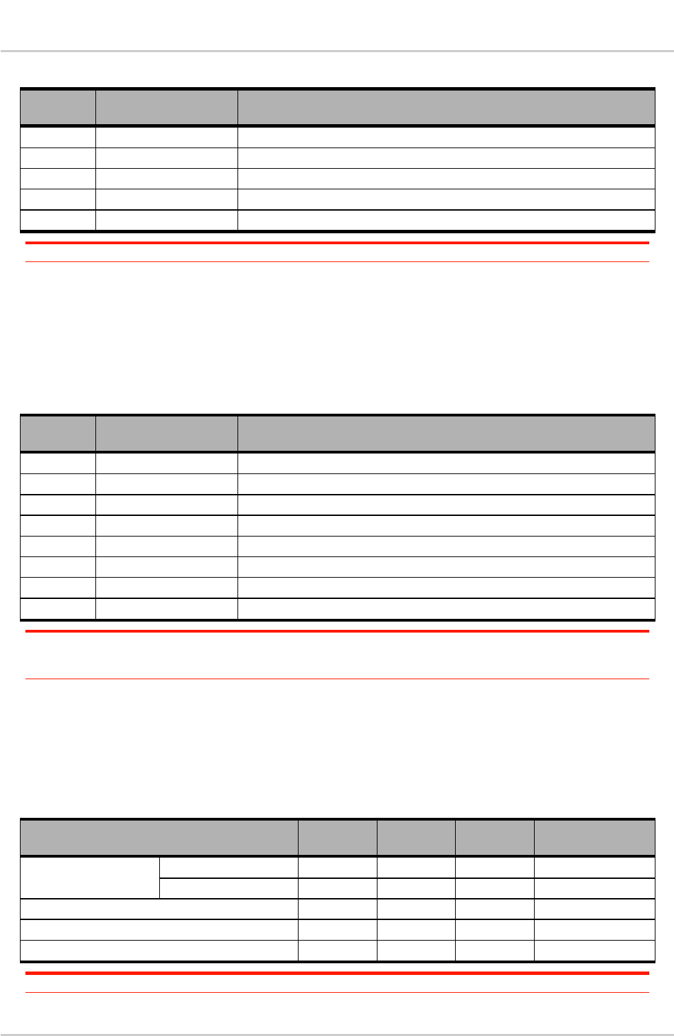
4114016 Rev 3.0 January 28, 2014 36
Product Technical Specification
Detailed Interface Specifications
Table 24. SPI Pin Description
Pad #
Name
Function
44
SPI1_SRDY
SPI Slave Ready
51
SPI1_MRDY
SPI Master Ready
52
SPI1_MISO
SPI Master In Slave Out
53
SPI1_CLK
SPI Clock
54
SPI1_MOSI
SPI Master Out Slave In
Note: It is strongly recommended to provide access through Test Points to this interface.
3.14.2. JTAG
The JTAG interface provides debug access to the core of the AirPrime HL6528x module. These JTAG
signals are accessible through solderable Test Points.
Table 25. JTAG Pin Description
Pad #
Name
Function
47
TP1
Test Point 1
236
JTAG_RESET
JTAG RESET
237
JTAG_TCK
JTAG Test Clock
238
JTAG_TDO
JTAG Test Data Output
239
JTAG_TMS
JTAG Test Mode Select
240
JTAG_TRST
JTAG Test Reset
241
JTAG_TDI
JTAG Test Data Input
242
JTAG_RTCK
JTAG Returned Test Clock
Note: It’s recommended to provide access through Test Points to the JTAG interface pins (for failure
analysis and HL6528x debugging). All signals listed in the table above shall be outputs on the
customer board to allow JTAG debugging.
3.15. PPS (HL6528-G and HL6528-G2.8V only)
The PPS signal is an output pulse related to GPS receiver time.
Table 26. PPS Electrical Characteristics
Parameter
Minimum
Typical
Maximum
Conditions
Voltage Level (V)
HL6528-G
1.70
1.80
1.90
HL6528-G2.8V
2.65
2.8
2.95
Frequency (Hz)
1
Pulse width (ms)
250
Synchronization to GPS time (µs)
1
Note: This output is available only when GNSS is in tracking mode.
4114016 Rev 3.0 January 28, 2014 37
Product Technical Specification
Detailed Interface Specifications
3.16. EXT_LNA_GPS_EN (HL6528-G and HL6528-
G2.8V only)
EXT_LNA_GPS_EN ON indicates whether the GNSS receiver is active and can be used to enable an
external LNA (or active antenna), especially during GNSS low power mode.
Table 27. EXT_LNA_GPS_EN Electrical Characteristics
Parameter
Minimum
Typical
Maximum
Conditions
Voltage Level (V)
HL6528-G
1.70
1.80
1.90
HL6528-G2.8V
2.65
2.8
2.95
3.17. RF Interface
The GSM RF interface of the AirPrime HL6528x module allows the transmission of RF signals. This
interface has a 50Ω nominal impedance.
3.17.1. RF Connection
A 50Ω stripline can be used to connect to standard RF connectors such as SMA, UFL, etc. for
antenna connection.
Table 28. RF Connection
RF Signal
Impedance
VSWR Rx (max)
VSWR Tx (max)
RF_MAIN
50Ω
3:1
3:1
3.17.2. RF Performances
RF performances are compliant with the ETSI recommendation GSM 05.05.
Frequency Band
Typical Sensitivity
Minimum Sensitivity
GSM850 (dBm)
-109.9
-107
EGSM (dBm)
-109.7
-107
DCS (dBm)
-109.5
-106
PCS (dBm)
-108.2
-106
Note: Values given above are average values across the frequency band.
3.17.3. TX Burst Indicator (2G_TX_ON)
The AirPrime HL6528x module provides a signal, 2G_TX_ON, for TX burst indication. 2G_TX_ON is a
2.8V signal and its status depends on the module transmitter state.
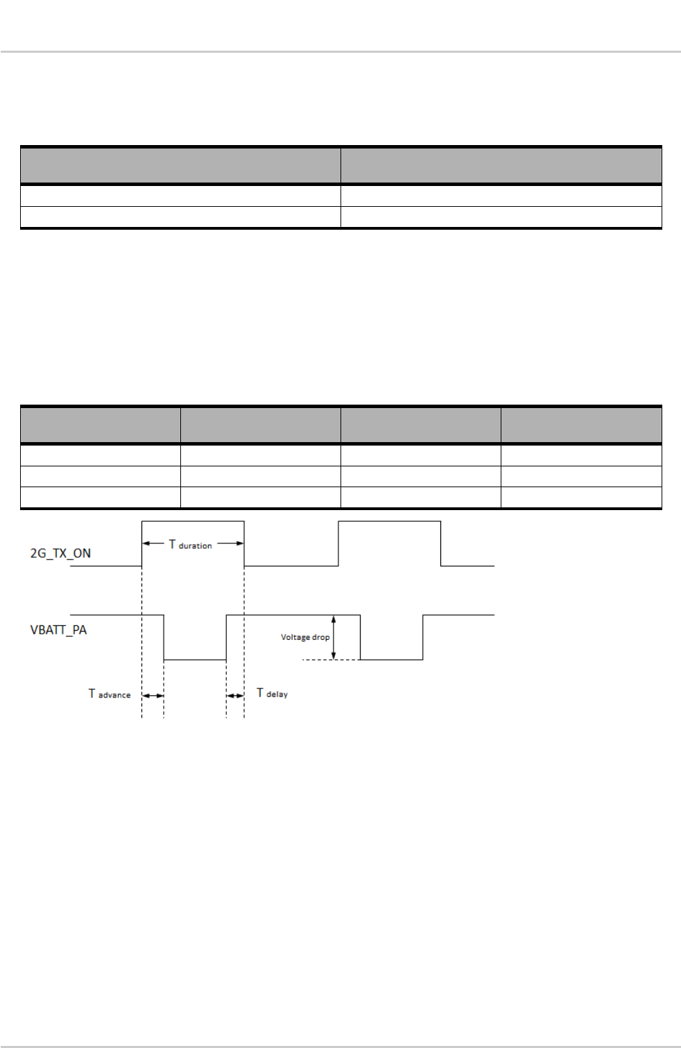
4114016 Rev 3.0 January 28, 2014 38
Product Technical Specification
Detailed Interface Specifications
Refer to the following table for the status of the 2G_TX_ON signal depending on the embedded
module’s state.
Table 29. Burst Indicator States
Embedded Module State
2G_TX_ON
During TX burst
High
No TX
Low
During TX burst, there is a higher current drain from the VBATT_PA power supply which causes a
voltage drop. This voltage drop from VBATT_PA is a good indication of a high current drain situation
during TX burst.
The blinking frequency is about 217Hz.
The output logic high duration, Tduration, depends on the number of TX slots and is computed as follows:
T duration = T advance + (0.577ms x number of TX slots) + T delay
Table 30. TX Burst Characteristics
Parameter
Minimum
Typical
Maximum
Output voltage (V)
2.65
2.80
2.95
Tadvance (µs)
30
180
Tdelay (µs)
0
10
Figure 7. 2G_TX_ON State during TX Burst
3.18. GNSS Interface
The AirPrime HL6528-G and HL6528-G2.8V modules embed an integrated and high-sensitivity Global
Navigation Satellite System (GNSS) solution.
Based on SiRFstarV™ from CSR, the AirPrime HL6528-G and HL6528-G2.8V modules combine GPS
and GLONASS reception to improve navigation capabilities and position accuracy in obstructed view
environments such as urban canyons. GNSS performances are improved by CW jammer and
interference mitigation system and automated hardware blanking capabilities.
In addition, it supports Downloaded Extended Ephemeris Assisted-GNSS, for enhanced time to
acquire or reacquire a fix.
The operation of GNSS is offloaded to a GNSS standalone solution to guarantee the availability of
modem resources for best performance.
4114016 Rev 3.0 January 28, 2014 39
Product Technical Specification
Detailed Interface Specifications
The GNSS implementation supports GPS L1 signal (1575.42 ± 20 MHz) and GLONASS L1 FDMA
signals for frequency -7 to 6 (1597.5 – 1605.8 MHz), with 50Ω connection on the RF_GPS pad.
3.18.1. GNSS Performances
Table 31. GNSS Interface Specifications
Test
Parameters
Typical Value
Sensitivity
GPS Autonomous Acquisition (dBm)
Cold and Warm start conditions
-147
GPS Autonomous Acquisition (dBm)
Hot start conditions
-159
GPS Navigation (dBm)
-161
GLONASS Navigation (dBm)
-158
GNSS Navigation (dBm)
-161
GPS Tracking (dBm)
-165
GLONASS Tracking (dBm)
-165
Autonomous Cold Start
Time To First Fix (s)
50%
23.3
95%
34.3
2D Position Error (m)
50%
0.86
95%
1.63
Autonomous Warm Start
Time To First Fix (s)
50%
19.5
95%
34.4
2D Position Error (m)
50%
0.16
95%
0.41
Autonomous Hot Start
Time To First Fix (s)
50%
0.7
95%
1
2D Position Error (m)
50%
3.8
95%
8.4
Aiding Warm Start
Time To First Fix (s)
50%
TBD
95%
TBD
2D Position Error (m)
50%
TBD
95%
TBD
Note: Values in the table above are based on static conditions, RF GNSS level @-130dBm. Cold start
does not include internal GNSS firmware download on first GNSS start.
3.18.2. GNSS Antenna Interface
Specifications for the GNSS antenna interface are defined in the table below.
Table 32. GNSS Antenna Specifications
Characteristics
GNSS
Frequency (MHz)
GPS L1
1575.42±20
GLONASS L1 FDMA
1597.5-1605.8
4114016 Rev 3.0 January 28, 2014 40
Product Technical Specification
Detailed Interface Specifications
Characteristics
GNSS
RF Impedance (Ω)
50
VSWR max
2:1
The minimum isolation between GNSS and GSM antennas should be 20dB.
3.18.3. GNSS Antenna Recommendations
Both passive and active antennas are supported by the AirPrime HL6528-G and HL6528-G2.8V
modules.
The table below describes the expected performance function as input signal power.
Table 33. GNSS Antenna Recommendations
GNSS Signal Level Description
Input Signal
Power (dBm)
Expected Performances
Absolute maximum
-110
Maximum to input level
Good
>-134
Best performance in TTFF and position accuracy
Acceptable
>-147
Minimum input level to allow initial acquisition
without aiding
Poor
<-147
No signal acquisition without aiding
Minimum usable signal
-161
Below this level, no fix with reasonable error
Minimum tracking level
-165
Minimum level to lock the signal for fast recovery
when the signal returns to the minimum usable
level
For passive antennas, the internal LNA should be set in high gain mode.
For active antennas, the internal LNA gain should be set to low gain if external net gain is higher than
16dB. If the external net gain is lower than 16dB, it is advised to set the internal LNA gain in high gain.
In any case, the external net gain should not exceed 24dB.
3.19. GPIO RESET/ DEFAULT states
Table 34. Pad Description
Pin
#
Signal Name
Function
I/O
RESET
STATE
RESET
VALUE
DEFAULT
STATE
DEFAULT
VALUE
1
GPIO1/I2C1_C
LK
General purpose
input/output/I2C Clock
I/O
2
UART1_RI
UART1: Ring indicator
O
3
UART1_RTS
UART1: Request to
send
I
4
UART1_CTS
UART1: Clear to send
O
5
UART1_TX
UART1: Transmit data
I
6
UART1_RX
UART1: Receive data
O
7
UART1_DTR
UART1: Data terminal
ready
I

4114016 Rev 3.0 January 28, 2014 41
Product Technical Specification
Detailed Interface Specifications
Pin
#
Signal Name
Function
I/O
RESET
STATE
RESET
VALUE
DEFAULT
STATE
DEFAULT
VALUE
8
UART1_DCD
UART1: Data carrier
detect
O
9
UART1_DSR
UART1: Data set
ready
O
10
GPIO2
General purpose
input/output
I/O
11
RESET_IN
Input reset signal
I
12
NC
Not Connected
13
NC
Not Connected
14
NC
Not Connected
15
NC
Not Connected
16
NC
Not Connected
17
SPKR_N
Speaker negative
output
(32Ω impedance)
O
18
SPKR_P
Speaker positive
output
(32Ω impedance)
O
19
MIC_P
Microphone positive
input
I
20
MIC_N
Microphone negative
input
I
21
BAT_RTC
Power supply for RTC
backup
I/O
22
TP2
Factory use only
0 – JTAGBoundary
Scan Mode
Open – Normal Mode
I
23
NC
Not Connected
24
ADC1
Analog to digital
conversion
I
25
ADC0
Analog to digital
conversion
I
26
UIM1_VCC
1.8V/3V UIM1 Power
supply
O
27
UIM1_CLK
1.8V/3V UIM1 Clock
O
28
UIM1_DATA
1.8V/3V UIM1 Data
I/O
29
UIM1_RESET
1.8V/3V UIM1 Reset
O
30
NC
NC (Reserved for 3G
compatibility)
31
NC
NC (Reserved for 3G
compatibility)
32
NC
NC (Reserved for 3G
compatibility)
33
PCM_OUT
PCM data out
O
34
PCM_IN
PCM data in
I
35
PCM_SYNC
PCM sync out
I/O

4114016 Rev 3.0 January 28, 2014 42
Product Technical Specification
Detailed Interface Specifications
Pin
#
Signal Name
Function
I/O
RESET
STATE
RESET
VALUE
DEFAULT
STATE
DEFAULT
VALUE
36
PCM_CLK
PCM clock
I/O
37
GND
Ground
GND
38
RF_GPS*
RF GPS Input
I
39
GND
Ground
GND
40
GPIO7
General purpose
input/output
I/O
41
GPIO8
General purpose
input/output
I/O
42
PPS*
GPS Pulse Per
Second
O
43
EXT_LNA_GP
S_EN*
External GPS LNA
enable
O
44
SPI1_SRDY
Debug use only
SPI Slave Ready
I
45
VGPIO
GPIO voltage output
O
46
GPIO6
General purpose
input/output
I/O
47
TP1
Test Point 1
0- JTAG Enable
Open-Normal Mode
I
48
GND
Ground
GND
49
RF_MAIN
RF GSM Input/output
I/O
50
GND
Ground
GND
51
SPI1_MRDY
Debug use only
SPI Master Ready
O
52
SPI1_MISO
Debug use only
SPI Master In Slave
Out
I
53
SPI1_CLK
Debug use only
SPI Clock
O
54
SPI1_MOSI
Debug use only
SPI Master Out Slave
In
O
55
UIM2_VCC
UIM2 Power supply
O
56
UIM2_DATA
UIM2 Data
I/O
57
UIM2_RESET/
BUZZER
UIM2 Reset/Buzzer
O
58
UIM2_CLK/PW
M
UIM2 Clock/PWM
O
59
PWR_ON
Active Low Power On
control signal
I/O
60
2G_TX_ON
2G TX burst indicator
O
61
VBATT_PA
3.7V Power Amplifier
Power supply
I
62
VBATT_PA
3.7V Power Amplifier
Power supply
I
63
VBATT
3.7V Power supply
I
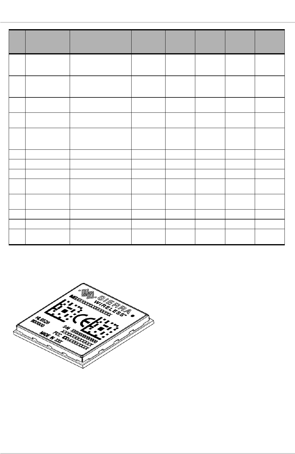
4114016 Rev 3.0 January 28, 2014 43
Product Technical Specification
Mechanical Drawings
Pin
#
Signal Name
Function
I/O
RESET
STATE
RESET
VALUE
DEFAULT
STATE
DEFAULT
VALUE
64
UIM1_DET/GPI
O3
UIM1
Detection/General
purpose input/output
I/O
65
UIM2_DET/GPI
O4
UIM2
Detection/General
purpose input/output
I/O
66
GPIO5/I2C1_D
ATA
General purpose
input/output/I²C DATA
I/O
67-
70
GND
Ground
GND
167
-
234
GND
GND
GND
235
TEST_PIN
Ground (Test Point)
GND
236
JTAG_RESET
JTAG RESET
I
237
JTAG_TCK
JTAG Test Clock
I
238
JTAG_TDO
JTAG Test Data
Output
O
239
JTAG_TMS
JTAG Test Mode
Select
I
240
JTAG_TRST
JTAG Test Reset
I
241
JTAG_TDI
JTAG Test Data Input
I
242
JTAG_RTCK
JTAG Returned Test
Clock
O
4. Mechanical Drawings
Figure 8. AirPrime HL6528x (angular view)
4114016 Rev 3.0 January 28, 2014 44
Product Technical Specification
Mechanical Drawings
Figure 9. AirPrime HL6528x (side view)
Figure 10. AirPrime HL6528x Module (top view)
4114016 Rev 3.0 January 28, 2014 45
Product Technical Specification
Mechanical Drawings
Figure 11. AirPrime HL6528x Module (bottom view with dimensions)
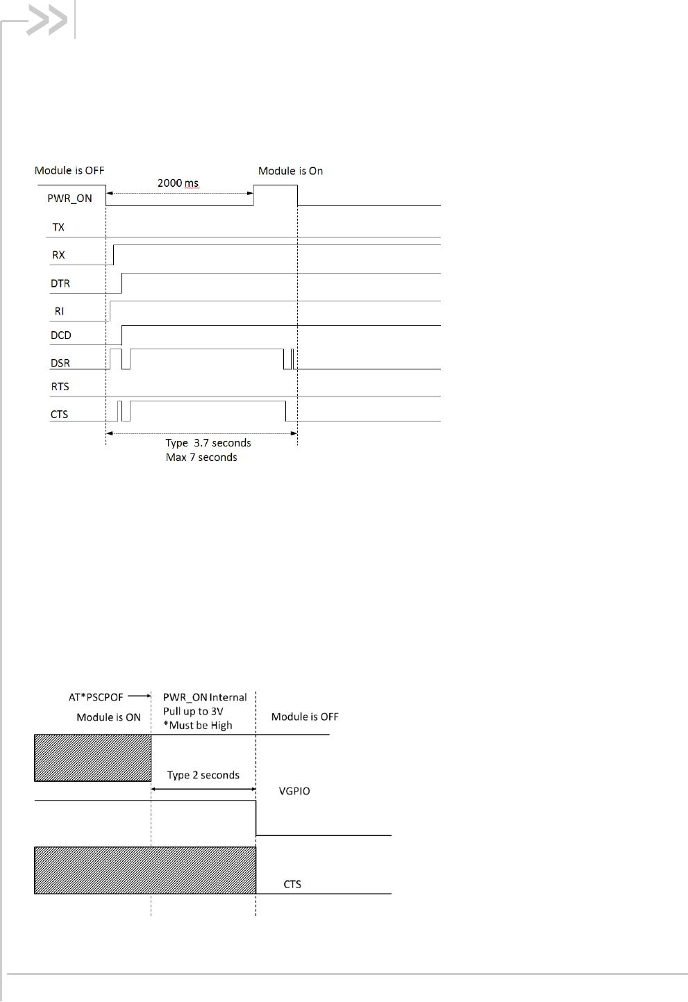
4114016 Rev 3.0 January 28, 2014 46
5. Design Guidelines
5.1. Power-Up Sequence
Apply a LOW level logic to the PWR_ON pin (pin 59). When CTS is toggling to low level, the module
is ready to receive AT commands.
Figure 12. UART Signals during the Power ON Sequence
5.2. Module Switch-Off
AT command AT*PSCPOF enables the user to properly switch the AirPrime HL6528x module off.
If required, the module can be switched off by controlling the power supply. This can be used, for
example, when the system freezes and no reset line is connected to the AirPrime HL6528x module. In
this case, the only way to get control back over the module is to switch off the power line.
VGPIO, PWR_ON and CTS signal behavior during the power off sequence is described in the figure
below.
Figure 13. Power OFF Sequence for PWR_ON, VGPIO and CTS
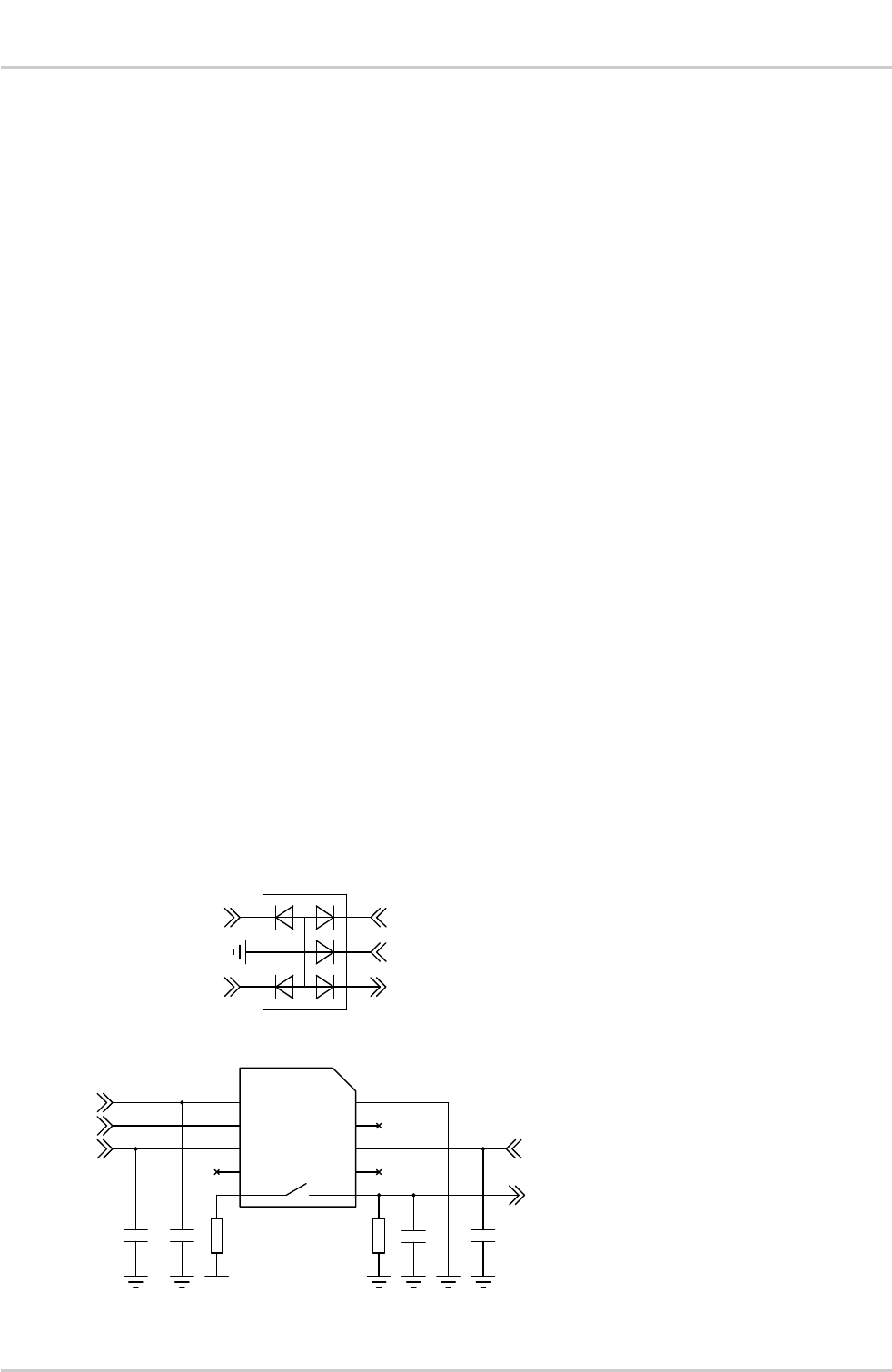
4114016 Rev 3.0 January 28, 2014 47
Product Technical Specification
Design Guidelines
5.3. Sleep Mode Management
AT command AT+KSLEEP enables the sleep mode configuration.
AT+KSLEEP=0:
The AirPrime HL6528x module is active when DTR signal is active (low electrical level).
When DTR is deactivated (high electrical level), the AirPrime HL6528x module enters sleep
mode after a while.
On DTR activation (low electrical level), the AirPrime HL6528x module wakes up.
AT+KSLEEP=1:
The AirPrime HL6528x module determines when it enters sleep mode (when no more tasks
are running).
“0x00” character on the serial link wakes the AirPrime HL6528x module up.
AT+KSLEEP=2:
The AirPrime HL6528x module never enters sleep mode.
In sleep mode, the module reduces its power consumption and remains waiting for the wake up
signals either from the network (i.e. read paging block depending on the DRX value of the network) or
the operating system (i.e. timers wake up timers activated) or the host controller (i.e. character on
serial link or DTR signal).
5.4. ESD Guidelines for UIM Cards
Decoupling capacitors must be added as close as possible to the UIM card connectors on UIM_CLK,
UIM_RST, UIM_VCC and UIM_DATA signals to avoid EMC issues and to pass the UIM card type
approval tests, according to the drawings below (this applies to both UIM slots, UIM1 and UIM2).
A typical schematic for hardware UIM detection is provided below.
Figure 14. EMC and ESD Components Close to the UIM
1 Vcc
2 RST
3 CLK
4 C4
I/O 7
VPP 6
GND 5
C8 8
9 SW_A
UIM_DATA
UIM_VCC
UIM_RESET
UIM_CLK
100nF
DNI
DNI
UIM_VCC
UIM_DATA
UIM_RESET
UIM_CLK
GPIOx
1K
SW_B 10 GPIOx
100K
1nF
VGPIO
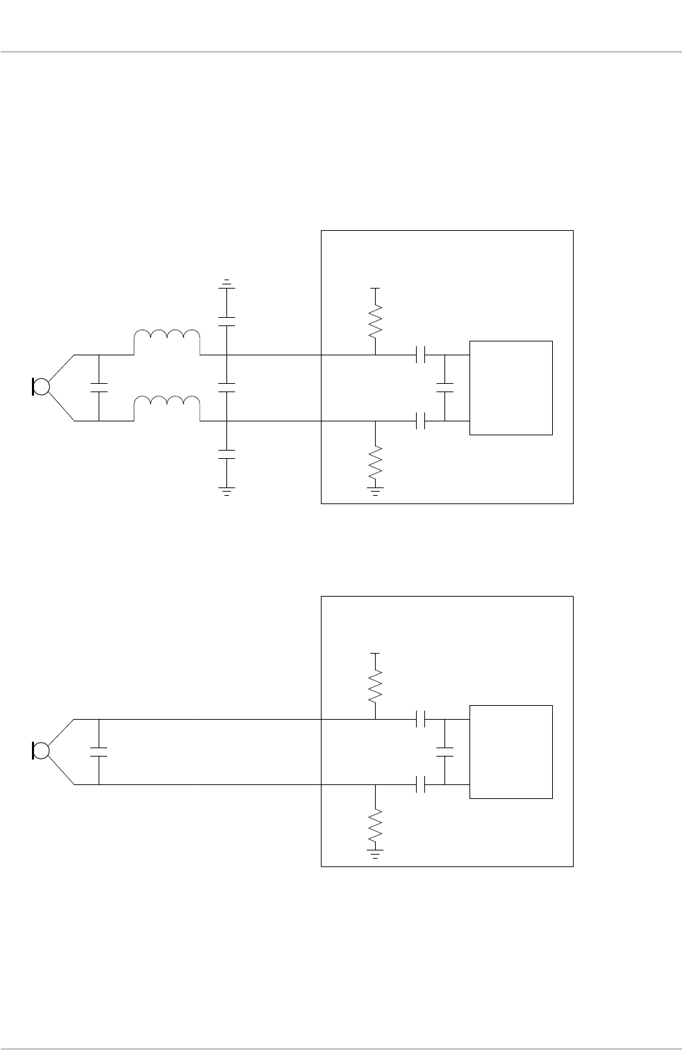
4114016 Rev 3.0 January 28, 2014 48
Product Technical Specification
Design Guidelines
5.5. Audio Integration
5.5.1. Microphone Audio Design
5.5.1.1. Differential Connection Example
MIC
L1
AUDIO
ADC
2.4V Typ. Internal MIC Bias
Z2*=2.2kΩ
100nF
100nF
18pF
MIC_P
MIC_N
L2
C1
C2
C3
C4
HL6528x
Z2*=2.2kΩ
Figure 15. Example of a MIC Input Connection with LC Filter
The LC filter (L1, L2, C2, C3, and C4) is used to reduce EMI perturbation created by TDMA noise, but
it is not mandatory. Good quality audio can be achieved without an LC filter depending on the design.
MIC AUDIO
ADC
2.4V Typ. Internal MIC Bias
Z2*=2.2kΩ
100nF
100nF
18pF
MIC_P
MIC_N
C1
HL6528x
Z2*=2.2kΩ
Figure 16. Example of a MIC Input Connection without LC Filter
Capacitor C1 is highly recommended to eliminate TDMA noise. Note that C1 must be close to the
microphone.
Refer to the table below for the recommended components to use with a microphone connection.
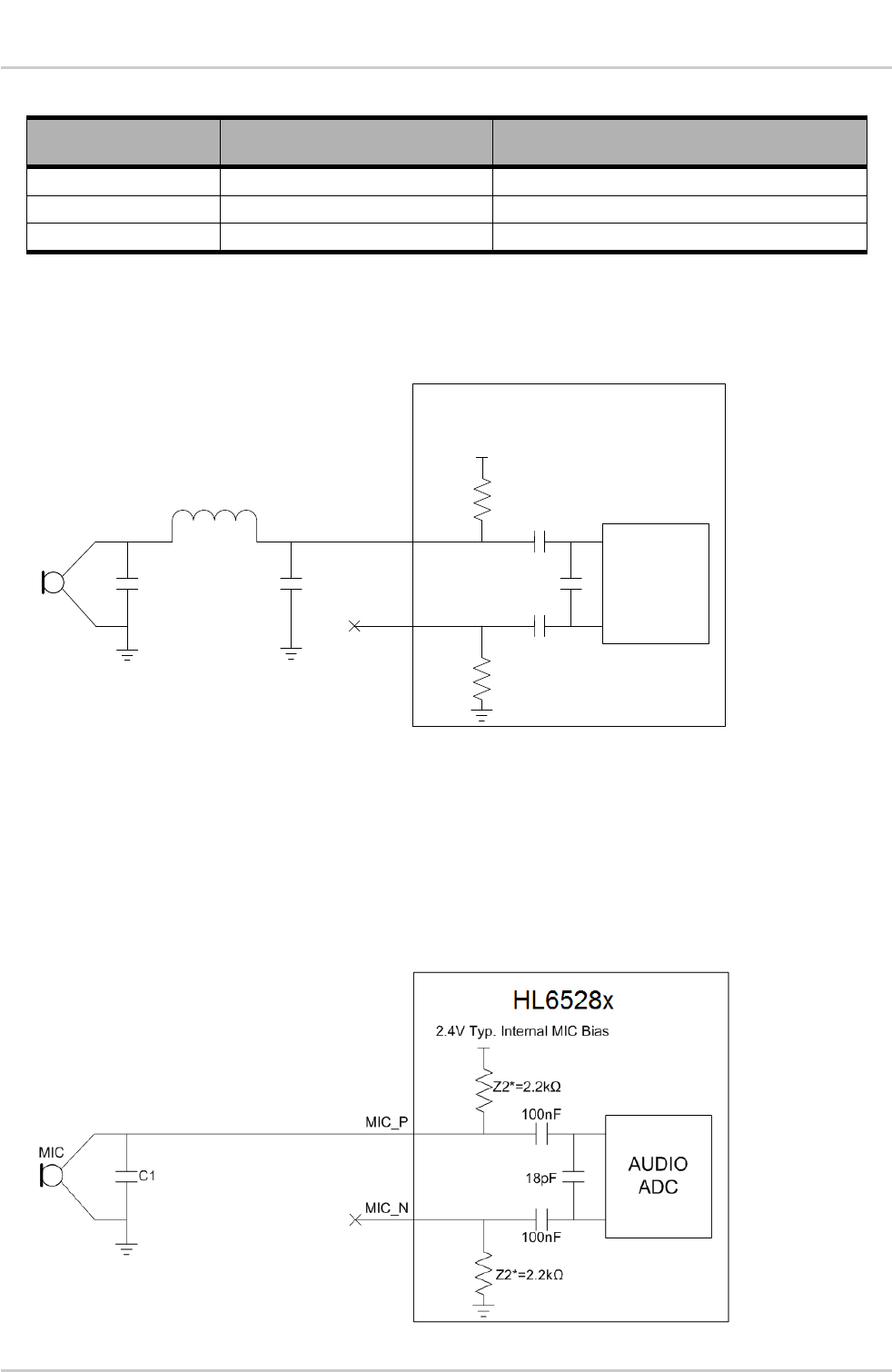
4114016 Rev 3.0 January 28, 2014 49
Product Technical Specification
Design Guidelines
Table 35. Recommended Components for a Microphone Connection
Component
Description/Details
Notes
C1
12pF to 33pF
Needs to be tuned depending on the design
C2, C3, C4
47pF
Needs to be tuned depending on the design
L1, L2
100nH
Needs to be tuned depending on the design
5.5.1.2. Single-Ended Connection Example
When a single-ended connection is used for MIC, MIC_N is just left open.
MIC
L1
AUDIO
ADC
2.4V Typ. Internal MIC Bias
Z2*=2.2kΩ
100nF
100nF
18pF
MIC_P
MIC_N
C1 C2
HL6528x
Z2*=2.2kΩ
Figure 17. Example of a Single-Ended MIC Input Connection with LC Filter
The internal input impedance value becomes 1100Ω due to the connection of the other end to ground.
The single-ended design is very sensitive to TDMA noise; it is recommended to add L1 and C2
footprint as an LC filter to try to eliminate TDMA noise. Very good grounding on the MIC is required in
order to ensure good performance against TDMA. Also, special care on the PCB layout must be
taken.
When not used, the filter can be removed by replacing L1 with a 0Ω resistor and by disconnecting C2,
as shown in the following figure.
Figure 18. Example of a Single-Ended MIC Input Connection without LC Filter
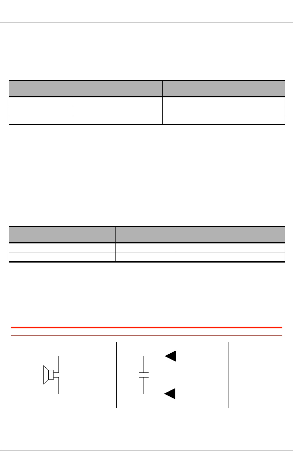
4114016 Rev 3.0 January 28, 2014 50
Product Technical Specification
Design Guidelines
The capacitor C1 is highly recommended to eliminate TDMA noise, and it must be placed close to the
microphone.
Refer to the table below for the recommended components to use with a single-ended microphone
connection.
Table 36. Recommended Components for a Single-Ended Microphone Connection
Component
Description/Details
Notes
C1
12pF to 33pF
Needs to be tuned depending on the design
C2
12pF to 33pF
Needs to be tuned depending on the design
L1
100nH
Needs to be tuned depending on the design
5.5.2. Speaker Audio Design
The SPKR interface can be used in a single-ended or a differential connection. However, it is strongly
recommended to use a differential connection in order to reject common mode noise and TDMA
noise. Moreover, in single-ended mode, half (1/2) of the power is lost.
When using a single-ended connection, be sure to have a very good ground plane, very good filtering
as well as shielding in order to avoid any disturbance on the audio path.
The following table lists the typical values of both speaker output.
Table 37. Speaker Details
Parameter
Typical Value
Connection
Z (SPKR_P, SPKR_N) (Ω)
32
Differential mode
Z (SPKR_P, SPKR_N) (Ω)
32
Single-ended mode
It is recommended to add ESD protection to the speaker when it is exposed to the external
environment. The ESD protection should be connected between the audio lines and a good ground,
and placed as close to the speaker as possible.
It is important to select an appropriate speaker and filtering components to avoid TDMA noise.
5.5.2.1.1. SPKR Differential Connection
Note: Add a 33pF capacitor between the SPKR_P and SPKR_N pins to reduce TDMA noise.
18pF
SPKR_P
SPKR_N
SPEAKER HL6528x
Figure 19. Example of a Differential Connection for SPKR
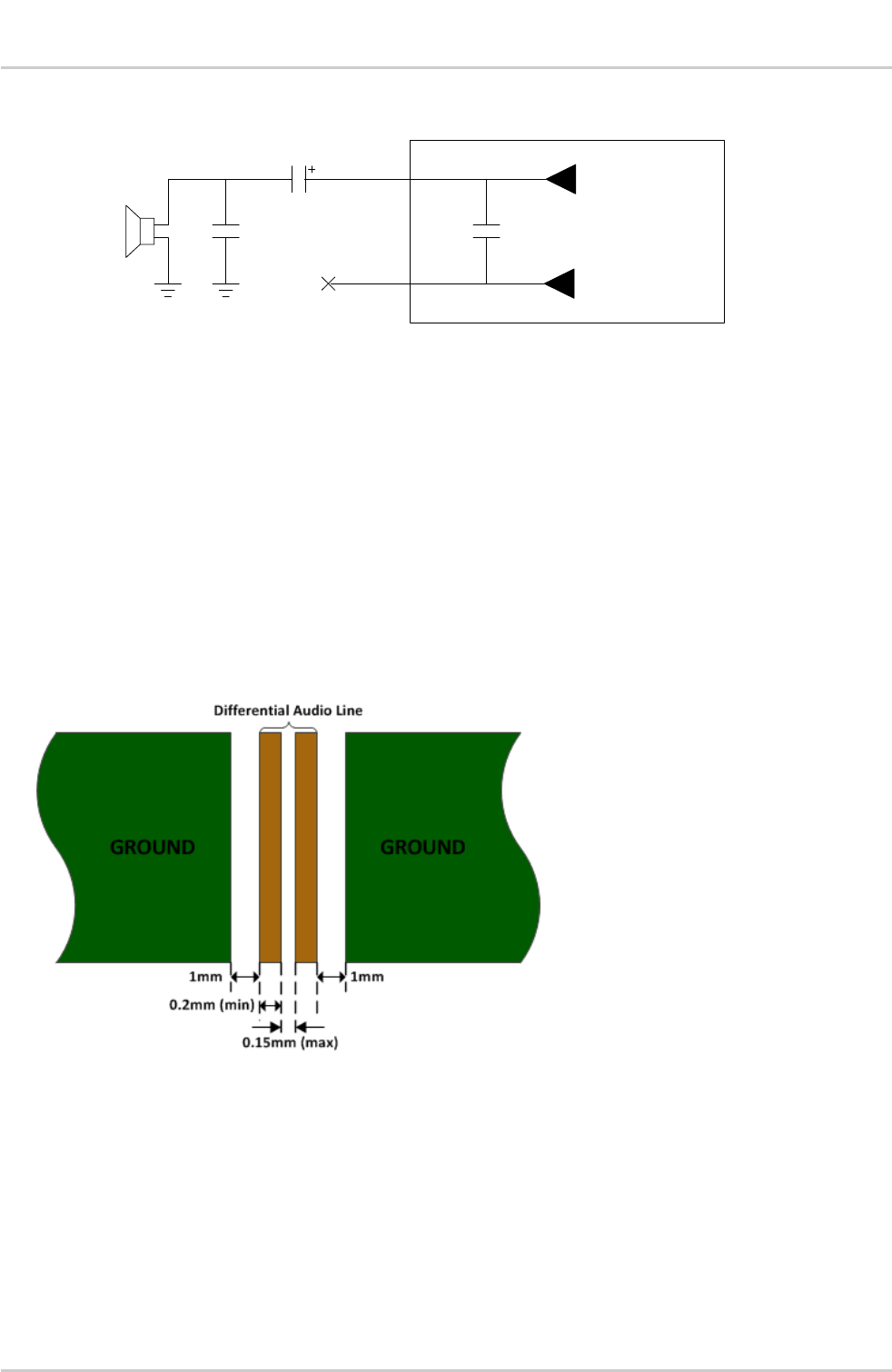
4114016 Rev 3.0 January 28, 2014 51
Product Technical Specification
Design Guidelines
5.5.2.1.2. SPKR Single-Ended Connection
18pF
SPKR_P
SPKR_N
SPEAKER HL6528x
C1
33pF~100pF
C3Z hp
Figure 20. Example of a Single-Ended Speaker Connection (typical implementation)
In a single-ended connection:
4.7µF < C1 < 47µF, depending on the speaker characteristics and output power
the connection between the AirPrime HL6528x module pins and the speaker must be
designed to keep the serial impedance lower than 1.5Ω
SPKR_N can be left open
output power is lost (-6dB) as compared to a differential connection
5.5.3. Audio Layout Guidelines
To avoid TDMA noise, it is recommended to surround the audio tracks with ground as shown in the
following figure.
Figure 21. Audio Track Design
For differential connections, refer to the on following figure. Note that the differential audio line is
always in parallel.
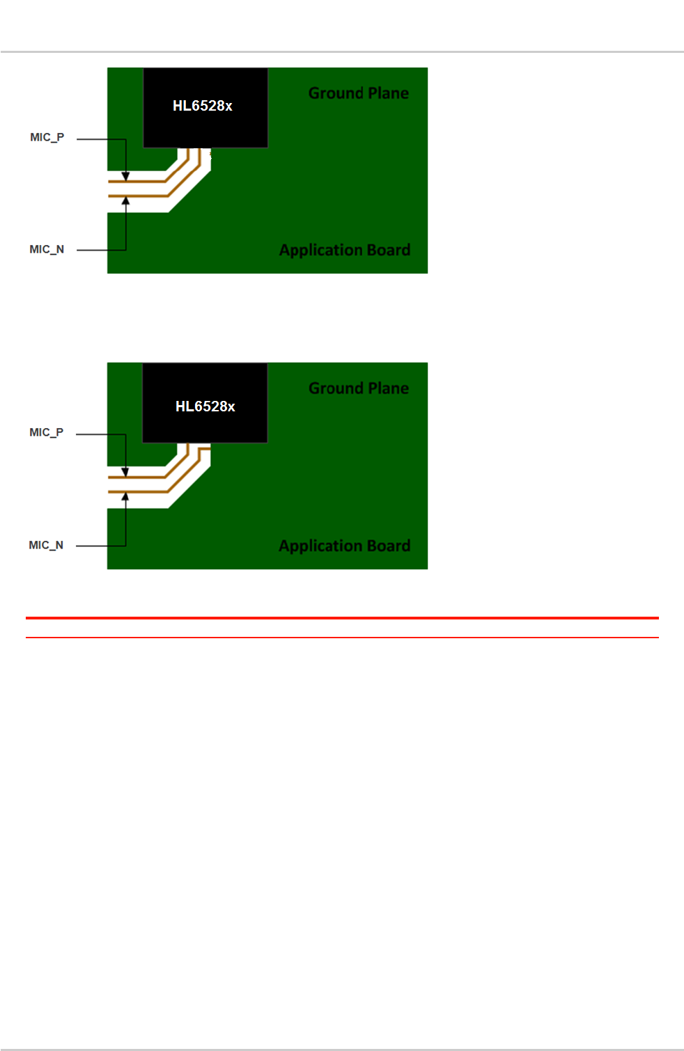
4114016 Rev 3.0 January 28, 2014 52
Product Technical Specification
Design Guidelines
Figure 22. Differential Audio Connection
For single-ended connections, the negative pole of the microphone, MIC_N, should be connected to
GND. Refer to the following figure.
Figure 23. Single-Ended Audio Connection
Caution: Avoid digital tracks crossing under and over the audio tracks.
It is highly recommended to have the MIC ground and the LC filter ground to act as an audio analog
ground during the PCB layout. This audio ground, together with the MIC_P signal, should act as the
differential line pair; and this audio ground should only be connected to the AirPrime HL6528x module
ground, as close as possible to the LGA GND pad of the AirPrime HL6528x module. It is the same
case for SPKR_P and SPKR_N.
Also, the audio interface is ESD sensitive. ESD protection MUST be added to the interface once it is
externally accessible.
To avoid distortion and burst noise, the following guidelines should be followed:
Audio signals must be symmetric (same components on each path)
Differential signals must be routed in parallel
Audio layer must be surrounded by 2 ground layers
The link from one component to the ground must be as short as possible
Separate the PCBs for the microphone and the speaker if possible
Reduce the number of electronic components as much as possible (to avoid loss of quality
and greater dispersion)
Audio tracks must be wider than 0.5 mm
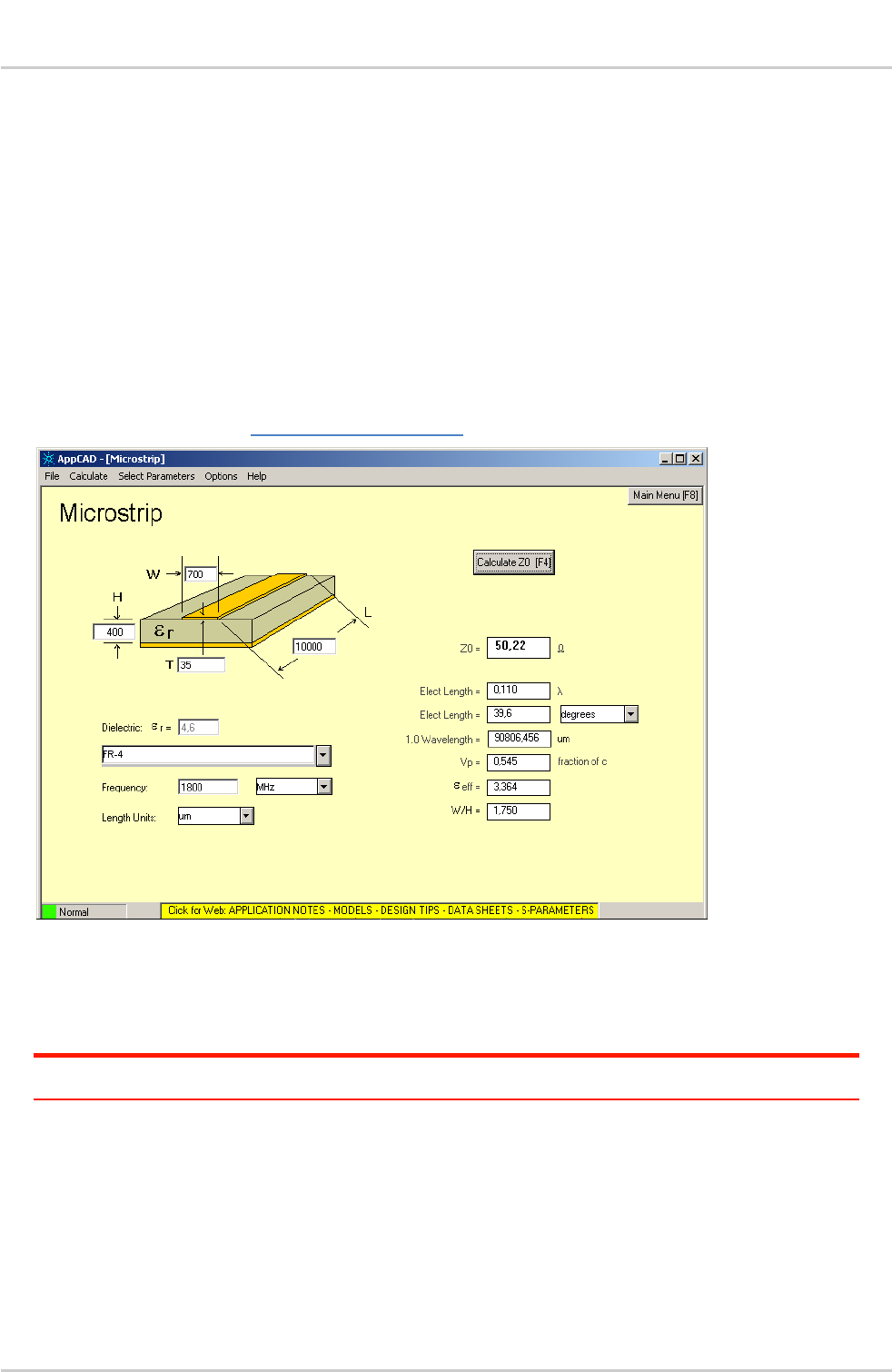
4114016 Rev 3.0 January 28, 2014 53
Product Technical Specification
Design Guidelines
5.6. Radio Integration
5.6.1. RF Routing Recommendations
To route the RF antenna signals, the following recommendations must be observed for PCB layout:
The RF signals must be routed using traces with a 50 characteristic impedance.
Basically, the characteristic impedance depends on the dielectric constant (εr) of the material used,
trace width (W), trace thickness (T), and height (H) between the trace and the reference ground plane.
In order to respect this constraint, Sierra Wireless recommends that a MicroStrip structure be used
and trace width be computed with a simulation tool (such as AppCAD, shown in the figure below and
available free of charge at http://www.avagotech.com).
Figure 24. AppCAD Screenshot for Microstrip Design Power Mode Diagram
The trace width should be wide enough to maintain reasonable insertion loss and manufacturing
reliability. Cutting out inner layers of ground under the trace will increase the effective substrate
height; therefore, increasing the width of the RF trace.
Caution: It is critical that no other signals (digital, analog, or supply) cross under the RF path. The figure
below shows a generic example of good and poor routing techniques.
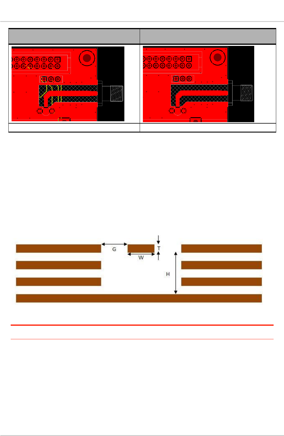
4114016 Rev 3.0 January 28, 2014 54
Product Technical Specification
Design Guidelines
Poor routing
Correct routing
The yellow traces cross the RF trace.
There is no signal around the RF path.
Figure 25. RF Routing Examples
Fill the area around the RF traces with ground and ground vias to connect inner ground layers
for isolation.
Cut out ground fill under RF signal pads to reduce stray capacitance losses.
Avoid routing RF traces with sharp corners. A smooth radius is recommended.
E.g. Use of 45° angles instead of 90°.
The ground reference plane should be a solid continuous plane under the trace.
The coplanar clearance (G, below) from the trace to the ground should be at least the trace
width (W) and at least twice the height (H). This reduces the parasitic capacitance, which
potentially alters the trace impedance and increases the losses.
E.g. If W = 100 microns then G = 200 microns in an ideal setup. G = 150 microns would also
be acceptable is space is limited.
Figure 26. Coplanar Clearance Example
Note: The figure above shows several internal ground layers cut out, which may not be necessary for
every application.
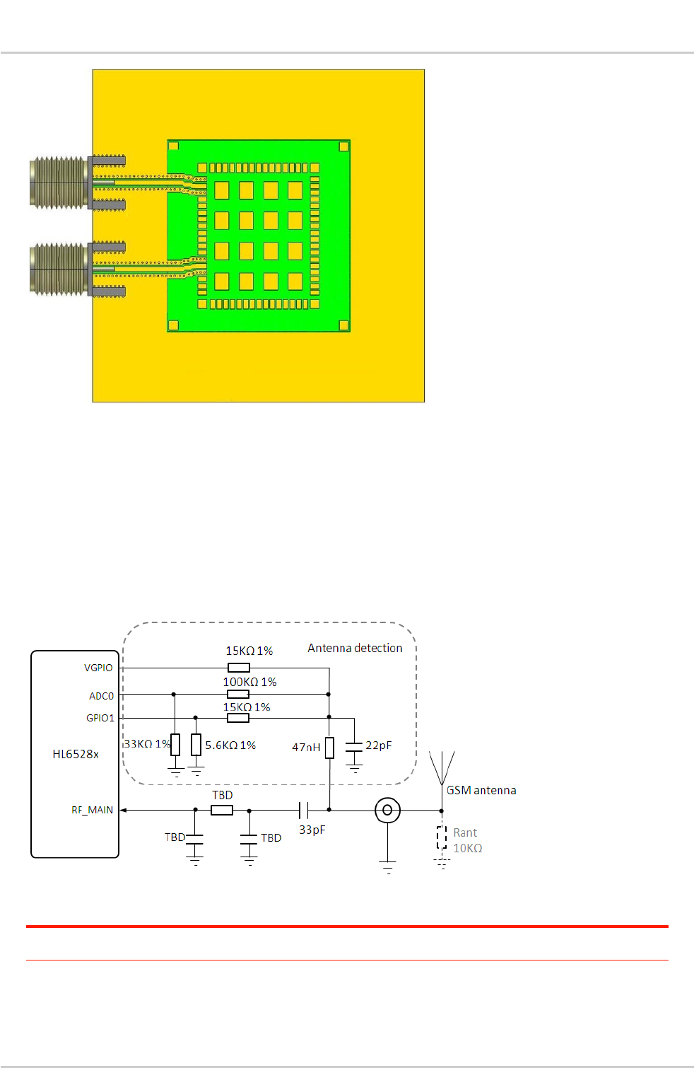
4114016 Rev 3.0 January 28, 2014 55
Product Technical Specification
Design Guidelines
Figure 27. Antenna Microstrip Routing Example
5.6.2. GSM Antenna Integration with Antenna
Detection Circuitry
The AirPrime HL6528x module is equipped with external antennas. A 50Ω line matching circuit
between the module, the customer’s board and the RF antennas is required, for GSM and GPS feed
path, as shown in the example below.
Figure 28. GSM Antenna Connection with Antenna Detection
Note: Antenna detection circuit is optional. Rant is the equivalent DC terminating resistor of the antenna.
Rant should be close to 10KΩ.
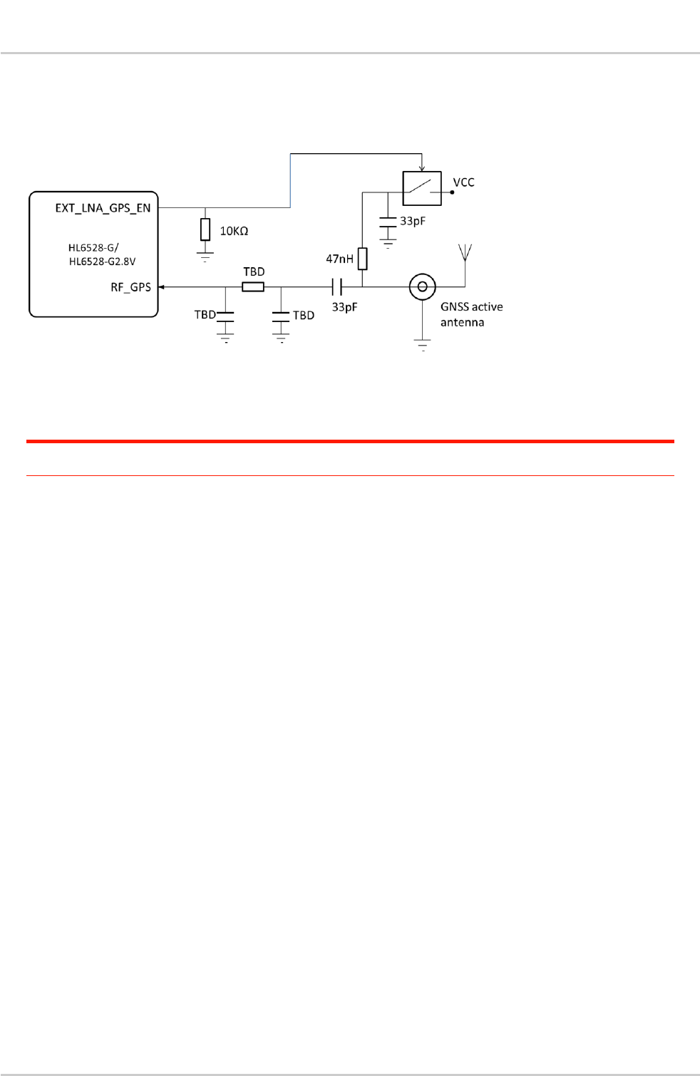
4114016 Rev 3.0 January 28, 2014 56
Product Technical Specification
Design Guidelines
5.6.3. GNSS Active Antenna Integration
The AirPrime HL6528-G and HL6528-G2.8V modules embed a GPS/GLONASS receiver inside. A
possible implementation with an active GNSS antenna is defined below.
Figure 29. GNSS Application with Active Antenna
EXT_LNA_GPS_EN is a specific signal that automatically sets the AirPrime HL6528-G and HL6528-
G2.8V modules’ internal LNA to low gain when an external pull-down resistor is detected.
Note: When the application needs to monitor the active antenna current, current monitor devices can be
connected to any of the module’s GPIOs, and read with a dedicated AT command.

4114016 Rev 3.0 January 28, 2014 57
6. X-Ray Exposure
X-ray exposure results in an undesirable shift in programmed bit threshold voltage of the Flash
memory.
As a result, Sierra Wireless recommends avoiding any X-ray exposure during customer manufacturing
process to ensure software integrity and long term reliability.
In case X- ray inspection could not be eliminated from the customer manufacturing process, a variety
of mitigation methods should be implemented to lower the risk of potential failure:
Use of filter between source and module to minimize exposure to harmful soft X- ray
300µm Zn filter or 1mm Al filter are optimal
Zn and Al absorb soft X-ray to which silicon is particularly vulnerable, and transmit soft
and medium energy X-rays required to obtain good imaging
Minimize X-Ray dose
should be less than 10 RADs
KV peak should be less than 50KV peak
tube current should be less than 20µA
Maximize distance between source and the module
Minimize the X-ray time
use the shortest exposure time possible
sampling only, not 100% inspection
Note that these mitigation guidelines are for information only as it’s NOT possible to provide accurate
acceptable or unacceptable X- ray exposure criteria, e.g. maximum safe dose rate, maximum safe
exposure time, etc.
7. Flash memory endurance
As many embedded device, the AirPrime HL6528x module is using flash memory which are
guaranteed for a limited number of program/erasing cycles per sector (100,000 cycles). Although
state-of-the-art mechanism has been implemented to limit the number of writing/erasing cycles, Sierra
Wireless recommends using “writing” AT commands appropriately and with caution. Those AT
commands are identified in the AirPrime HL6 and HL8 Series AT Commands Interface Guide [2].
8. FCC/IC Legal Information
8.1. Label
The AirPrime HL6528x module is labeled with its own FCC ID on the shield side. Each HL6528x
variant has its own FCC ID as listed in the table below.

4114016 Rev 3.0 January 28, 2014 58
Product Technical Specification
FCC/IC Legal Information
Table 38. AirPrime HL6528x FCC IDs
Model Name
FCC ID
HL6528
N7NHL6528
HL6528-G
N7NHL6528G
HL6528-2.8V
N7NHL652828V
HL6528-G2.8V
N7NHL6528G28V
When the module is installed in a customer’s product, the FCC ID label on the module will not be
visible. To avoid this case, an exterior label must be stuck on the surface of the customer’s product to
indicate the FCC ID of the enclosed module. This label can use wording such as the following:
“Contains Transmitter module FCC ID: <FCC ID as listed in Table 38 AirPrime HL6528x FCC IDs>” or
“Contains FCC ID: <FCC ID as listed in Table 38 AirPrime HL6528x FCC IDs>”.
8.2. FCC Regulations
This device complies with part 15 of the FCC Rules. Operation is subject to the following two
conditions:
1. This device may not cause harmful interference, and
2. This device must accept any interference received, including interference that may cause
undesired operation.
This device has been tested and found to comply with the limits for a Class B digital device, pursuant
to Part 15 of the FCC Rules. These limits are designed to provide reasonable protection against
harmful interference in a residential installation. This equipment can radiate radio frequency energy
and, if not installed and used in accordance with the instructions, may cause harmful interference to
radio communications. However, there is no guarantee that interference will not occur in a particular
installation. If this equipment does cause harmful interference to radio or television reception, which
can be determined by turning the equipment off and on, the user is encouraged to try to correct the
interference by one or more of the following measures:
1. Reorient or relocate the receiving antenna
2. Increase the separation between the equipment and receiver.
3. Connect the equipment into an outlet on a circuit different from that to which the receiver is
connected.
4. Consult the dealer or an experienced radio/TV technician for help.
Changes or modifications not expressly approved by the party responsible for compliance could void
the user’s authority to operate the equipment.
8.3. RF Exposure Information
This Modular Approval is limited to OEM installation for mobile and fixed applications only. The
antenna installation and operating configurations of this transmitter, including any applicable source-
based time-averaging duty factor, antenna gain and cable loss must satisfy MPE categorical
Exclusion Requirements of §2.1091.
The antenna(s) used for this transmitter must be installed to provide a separation distance of at least
20 cm from all persons, must not be collocated or operating in conjunction with any other antenna or
transmitter, except in accordance with FCC multi-transmitter product procedures.
4114016 Rev 3.0 January 28, 2014 59
Product Technical Specification
FCC/IC Legal Information
The end user has no manual instructions to remove or install the device and a separate approval is
required for all other operating configurations, including portable configurations with respect to 2.1093
and different antenna configurations.
According to the MPE RF explore report, maximum antenna gain allowed for use with this device is
5.5dBi for GSM850 and 2.0dBi for PCS1900.
When the module is installed in the host device, the FCC ID label must be visible through a window
on the final device or it must be visible when an access panel, door or cover is easily removed.
Otherwise, a second label must be placed on the outside of the final device that contains the following
text: ―Contains FCC ID: <FCC ID as listed in Table 38 AirPrime HL6528x FCC IDs>
The HL6528X modem may transmit simultaneously with other collocated radio transmitters within a
host device, provided the following conditions are met:
·Each collocated radio transmitter has been certified by FCC / IC for mobile application.
·At least 20 cm separation distance between the antennas of the collocated transmitters and the
user’s body must be maintained at all times.
The output power and antenna gain must not exceed the limits and configurations stipulated in the
following table.
1.Valid collocated transmitter combinations: WLAN+BT;
WiMAX+BT.(WLAN+WiMAX+BT is not permitted.)
8.4. IC Regulations
IC Radiation Exposure Statement:
This equipment complies with IC RSS-102 radiation exposure limits set forth for an
uncontrolled environment. This equipment should be installed and operated with minimum
distance 20cm between the radiator & your body.
This device and its antenna(s) must not be co-located or operating in conjunction with any
other antenna or transmitter.
This Class B digital apparatus complies with Canadian ICES-003.
Under Industry Canada regulations, this radio transmitter may only operate using an antenna
of a type and maximum (or lesser) gain approved for the transmitter by Industry Canada. To
reduce potential radio interference to other users, the antenna type and its gain should be so
chosen that the equivalent isotropically radiated power (e.i.r.p) is not more than necessary for
successful communication.
Technoloty
Frequency (MHz)
Maximum
Conducted
Power (dBm)
Maximum Antenna
Gain (dBi)
Collocated
HL6528-
G2.8V
GPRS
824-849
34.0
2.5
1850 -1910
31.0
2.0
Collocated
Transmitters
WLAN
2400 -2500
29.0
5.0
WLAN
5150 -5850
29.0
5.0
WiMAX
2300 -2400
29
5.0
WiMAX
2500 -2700
29
5.0
WiMAX
3300 -3800
29
5.0
BT
2400 -2500
15
5.0

4114016 Rev 3.0 January 28, 2014 60
Product Technical Specification
FCC/IC Legal Information
Labeling Requirements for the Host Device (from Section 3.2.1, RSS-Gen, Issue 3,
December 2010): The host device shall be properly labeled to identify the module within the
host device. The Industry Canada certification label of a module shall be clearly visible at all
times when installed in the host device, otherwise the host device must be labeled to display
the Industry Canada certification number of the module, preceded by the words ― Contains
transmitter module‖, or the word ― Contains‖, or similar wording expressing the same
meaning, as follows: Contains transmitter module IC: <IC number as listed below>.
Table 39. AirPrime HL6528x IC number
Model Name
IC number
HL6528
2417C-HL6528
HL6528-G
2417C-HL6528G
HL6528-2.8V
2417C-HL652828V
HL6528-G2.8V
2417C-HL6528G28V
This device complies with Industry Canada license-exempt RSS standard(s). Operation is
subject to the following two conditions: (1) this device may not cause interference, and (2) this
device must accept any interference, including interference that may cause undesired
operation of the device. Le présent appareil est conforme aux CNR d'Industrie Canada
applicables aux appareils radio exempts de licence.
This radio transmitter (identify the device by certification number, or model number if
Category II) has been approved by Industry Canada to operate with the antenna types listed
below with the maximum permissible gain and required antenna impedance for each antenna
type indicated. Antenna types not included in this list, having a gain greater than the
maximum gain indicated for that type, are strictly prohibited for use with this device.

4114016 Rev 3.0 January 28, 2014 61
9. Ordering Information
Model Name
Part Number
Designation
HL6528
1102044
HL6528, GENERIC 1.8V
HL6528-G
1102045
HL6528-G, GENERIC 1.8V
HL6528-2.8V
1102047
HL6528-2.8V, GENERIC 2.8V
HL6528-G2.8V
1102048
HL6528-G2.8V, GENERIC 2.8V
DEV-KIT
6000575
DEV-KIT, HL6 series

4114016 Rev 3.0 January 28, 2014 62
10. Terms and Abbreviations
Abbreviation
Definition
ADC
Analog to Digital Converter
AGC
Automatic Gain Control
AT
Attention (prefix for modem commands)
AVL
Automatic Vehicle Location
CCB
Customer Carrier Board
CDMA
Code Division Multiple Access
CF3
Common Flexible Form Factor
CLK
Clock
CODEC
Coder Decoder
CPU
Central Processing Unit
DAC
Digital to Analog Converter
DTR
Data Terminal Ready
EGNOS
European Geostationary Navigation Overlay Service
EMC
ElectroMagnetic Compatibility
EMI
ElectroMagnetic Interference
EN
Enable
ESD
ElectroStatic Discharges
ETSI
European Telecommunications Standards Institute
FDMA
Frequency-division multiple access
GAGAN
GPS aided geo augmented navigation
GLONASS
GLObal NAvigation Satellite System
GND
Ground
GNSS
Global Navigation Satellite System
GPIO
General Purpose Input Output
GPRS
General Packet Radio Service
GSM
Global System for Mobile communications
Hi Z
High impedance (Z)
IC
Integrated Circuit
IMEI
International Mobile Equipment Identification
I/O
Input / Output
LED
Light Emitting Diode
LNA
Low Noise Amplifier
MAX
MAXimum
MIN
MINimum
MSAS
Multi-functional Satellite Augmentation System
N/A
Not Applicable
PA
Power Amplifier
PC
Personal Computer
PCB
Printed Circuit Board
PCL
Power Control Level

4114016 Rev 3.0 January 28, 2014 63
Product Technical Specification
Terms and Abbreviations
Abbreviation
Definition
PLL
Phase Lock Loop
PWM
Pulse Width Modulation
QZSS
Quasi-Zenith Satellite System
RF
Radio Frequency
RFI
Radio Frequency Interference
RMS
Root Mean Square
RST
Reset
RTC
Real Time Clock
RX
Receive
SCL
Serial Clock
SDA
Serial Data
SIM
Subscriber Identification Module
SMD
Surface Mounted Device/Design
SPI
Serial Peripheral Interface
SV
Satellite Vehicle
SW
SoftWare
PSRAM
Pseudo Static RAM
TBC
To Be Confirmed
TBD
To Be Defined
TP
Test Point
TTS
Text To Speech
TX
Transmit
TYP
Typical
UART
Universal Asynchronous Receiver-Transmitter
UICC
Universal Integrated Circuit Card
USB
Universal Serial Bus
UIM
User Identity Module
VBATT
Main Supply Voltage from Battery or DC adapter
VSWR
Voltage Standing Wave Ratio
WAAS
Wide Area Augmentation System