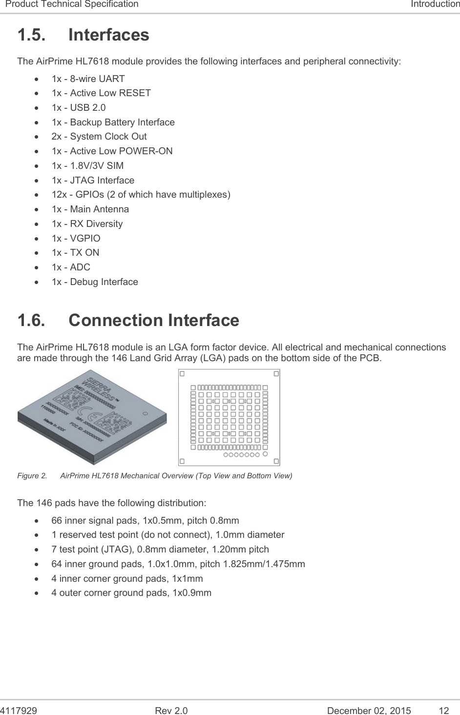
Sierra Wireless HL7618 Module User Manual
Sierra Wireless Inc. Module
UserManual.wiki
>
Sierra Wireless
>
HL7618 User Manual
User manual
Navigation menu
Upload a User Manual
Namespaces
Wiki Guide
HTML
PDF
Info
Views
User Manual
Discussion / Help
Navigation
![4117929 Rev 2.0 December 02, 2015 14 Product Technical Specification Introduction 1.8.2. Regulatory The AirPrime HL7618 is compliant with FCC regulations. FCC compliance will be reflected on the AirPrime HL7618 label. Table 5. Regulation Compliance Document Current Version Title GCF-CC v3.59.0 or later GCF Conformance Certification Criteria FCC Part 27 NA Miscellaneous wireless communication services 1.8.3. RoHS Directive Compliant The AirPrime HL7618 module is compliant with RoHS Directive 2011/65/EU which sets limits for the use of certain restricted hazardous substances. This directive states that “from 1st July 2006, new electrical and electronic equipment put on the market does not contain lead, mercury, cadmium, hexavalent chromium, polybrominated biphenyls (PBB) or polybrominated diphenyl ethers (PBDE)”. 1.8.4. Disposing of the Product This electronic product is subject to the EU Directive 2012/19/EU for Waste Electrical and Electronic Equipment (WEEE). As such, this product must not be disposed of at a municipal waste collection point. Please refer to local regulations for directions on how to dispose of this product in an environmental friendly manner. 1.9. References [1] AirPrime HL Series Customer Process Guidelines Reference Number: 4114330 [2] AirPrime HL7618, HL7690 and HL7692 AT Commands Interface Guide Reference Number: 4118395 [3] AirPrime HL Series Development Kit User Guide Reference Number: 4114877](https://usermanual.wiki/Sierra-Wireless/HL7618/User-Guide-2842124-Page-14.png)
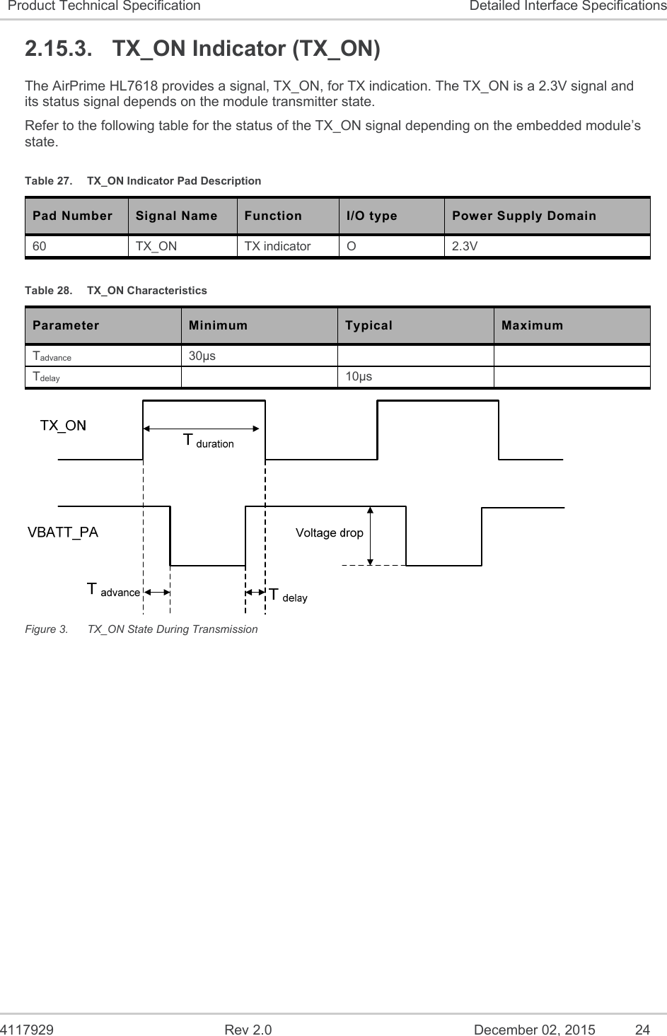
![4117929 Rev 2.0 December 02, 2015 22 Product Technical Specification Detailed Interface Specifications 2.13. Clock Interface The AirPrime HL7618 modules support two digital clock interfaces. The following table describes the pad description of the clock out interfaces. Table 21. Clock Interface Pad Description Pad Number Signal Name I/O I/O Type Description 22 26M_CLKOUT O 1.8V 26MHz Digital Clock output 23 32K_CLKOUT O 1.8V 32.768kHz Digital Clock output Enabling or disabling the clock out feature can be done using AT commands. For more information about AT commands, refer to document [2] AirPrime HL7618, HL7690 and HL7692 AT Commands Interface Guide. 2.14. Debug Interfaces The AirPrime HL7618 module provides 2 interfaces for a powerful debug system. 2.14.1. Trace Debug The AirPrime HL7618 module provides a Trace Debug interface, providing real-time instruction and data trace of the modem core. Table 22. Trace Debug Pad Description Pad Number Signal Name Function 2 TRACE_DATA3 Trace data 3 8 TRACE_DATA1 Trace data 1 9 TRACE_DATA0 Trace data 0 10 TRACE_DATA2 Trace data 2 41 TRACE_CLK Trace clock Note: It is strongly recommended to provide access to this interface through Test Points. 2.14.2. JTAG The JTAG interface provides debug access to the core of the HL7618. These JTAG signals are accessible through solder-able test points. Table 23. JTAG Pad Description Pad Number Signal Name Function 236 JTAG_RESET JTAG RESET 237 JTAG_TCK JTAG Test Clock](https://usermanual.wiki/Sierra-Wireless/HL7618/User-Guide-2842124-Page-22.png)