Sierra Wireless Q2438F-M TRI MODE CDMA WIRELESS MODULE KIT User Manual Starter Kit V2 User Guide
Sierra Wireless, Inc. TRI MODE CDMA WIRELESS MODULE KIT Starter Kit V2 User Guide
Contents
- 1. USERS MANUAL
- 2. Manual 1
- 3. Manual 2
- 4. Manual 3
USERS MANUAL

Confidential © Page: 1 / 18
This document is the sole and exclusive property of WAVECOM. Not to be distributed or divulged without prior written
agreement.
Ce document est la propriété exclusive de WAVECOM. Il ne peut être communiqué ou divulgué à des tiers sans son
autorisation préalable.
Q2438F-M/Starter Kit V2 User Guide
Reference: WI_HWD_SK_UGD_002
Level : 003
Date: June 1, 2005

WM_HWD_SK_UGD_002 - 002
6/1/2005
Confidential © Page: 2 / 18
This document is the sole and exclusive property of WAVECOM. Not to be distributed or divulged without prior written
agreement.
Ce document est la propriété exclusive de WAVECOM. Il ne peut être communiqué ou divulgué à des tiers sans son
autorisation préalable.
Document Information
Level Date History of the evolution Writer
001 23/9/2002 First draft RNixon
002 24/9/2002 Mechanical drawings update RNixon
003 27/6/2003 Add PDF Schematic RNixon
Name Function Date Signature
Written by Russ Nixon Hardware Engineer 23/9/02
Checked by
Approved by

WM_HWD_SK_UGD_002 - 002
6/1/2005
Confidential © Page: 3 / 18
This document is the sole and exclusive property of WAVECOM. Not to be distributed or divulged without prior written
agreement.
Ce document est la propriété exclusive de WAVECOM. Il ne peut être communiqué ou divulgué à des tiers sans son
autorisation préalable.
Contents
1 OVERVIEW............................................................................................................................................... 4
2 PRODUCT DESCRIPTION..................................................................................................................... 5
3 DESCRIPTION OF THE INTERFACES............................................................................................... 5
3.1 POWER.................................................................................................................................................. 5
3.2 COMPUTER ........................................................................................................................................... 6
3.2.1 DATA ........................................................................................................................................... 6
3.2.2 DM............................................................................................................................................... 6
3.3 SWITCHES AND JUMPERS ...................................................................................................................... 6
3.3.1 ON/OFF Switch ........................................................................................................................... 6
3.3.2 BOOT Switch ............................................................................................................................... 7
3.3.3 RESET Switch.............................................................................................................................. 7
3.3.4 SNGL/DIFF Jumper .................................................................................................................... 7
3.4 AUDIO .................................................................................................................................................. 7
3.4.1 Handset........................................................................................................................................ 7
3.4.2 Headset ........................................................................................................................................ 7
3.5 RF ........................................................................................................................................................ 8
3.5.2 FCC and Industry Canada Regulatory compliance..................................................................... 9
3.6 SIM SOCKET ...................................................................................................................................... 10
3.7 ADDITIONAL INTERFACES................................................................................................................... 10
3.7.1 Vibrator...................................................................................................................................... 10
3.7.2 Ringer ........................................................................................................................................ 11
3.7.3 GPIO.......................................................................................................................................... 11
3.7.4 Keypad....................................................................................................................................... 11
3.7.5 JTAG.......................................................................................................................................... 11
3.8 LED FUNCTION.................................................................................................................................. 12
3.8.1 LED1.......................................................................................................................................... 12
3.8.2 LED2.......................................................................................................................................... 12
4 START-UP ............................................................................................................................................... 12
4.1 CONNECTIONS .................................................................................................................................... 12
4.2 CONFIGURATION................................................................................................................................. 13
4.2.1 Computer ................................................................................................................................... 13
4.2.2 Power Supply............................................................................................................................. 13
4.2.3 Interface Board.......................................................................................................................... 13
5 TROUBLESHOOTING.......................................................................................................................... 14
5.1 NO RF SIGNAL.................................................................................................................................... 14
5.2 THE MODULE DOES NOT ANSWER THROUGH THE SERIAL LINK ........................................................... 14
5.3 NO AUDIO........................................................................................................................................... 14
6 INTERFACE BOARD PHYSICAL DRAWINGS................................................................................ 14
6.1 LAYOUT.............................................................................................................................................. 14
6.2 ASSEMBLY DRAWING......................................................................................................................... 16
6.3 ISOMETRIC.......................................................................................................................................... 17

WM_HWD_SK_UGD_002 - 002
6/1/2005
Confidential © Page: 4 / 18
This document is the sole and exclusive property of WAVECOM. Not to be distributed or divulged without prior written
agreement.
Ce document est la propriété exclusive de WAVECOM. Il ne peut être communiqué ou divulgué à des tiers sans son
autorisation préalable.
1 Overview
This Document is intended to provide the user complete instructions on the capabilities and use of
the Wavecom Starter Kit. The Wavecom Starter Kit is designed to allow the customer to interface to
the Wavecom Q2300 and Q2400 CDMA and GSM/GPRS Module families. Control of the Module is
done via AT Commands issued from an external PC running a terminal emulator, such as
HyperTerminal. The User should refer to the Wavecom CDMA AT Commands Interface
Specification for more information on supported commands.

WM_HWD_SK_UGD_002 - 002
6/1/2005
Confidential © Page: 5 / 18
This document is the sole and exclusive property of WAVECOM. Not to be distributed or divulged without prior written
agreement.
Ce document est la propriété exclusive de WAVECOM. Il ne peut être communiqué ou divulgué à des tiers sans son
autorisation préalable.
2 Product Description
The Wavecom Starter Kit includes the following:
Interface Board
The Interface Board provides a working platform for testing and evaluating the performance of the
Module, as well as allowing customer design of host software interfaces.
Module
One Wavecom module is included with the Starter Kit and comes pre-assembled on the Interface
Board. The Module is soldered down via its four Ground contact pins, and is also mated to the 60
pin board-to-board connector of the Interface Board.
Handset
The Handset contains a standard telephony earpiece and microphone, providing a full audio
interface to the Module through the Interface Board connectors.
Serial Cable
The Serial Cable connects the Interface Board to the controlling PC.
Antenna and RF Adapter
The Antenna provides sufficient omni-directional gain to allow the module to go over the air on the
network. An Antenna Adapter is provided to allow the Antenna Cable to connect to the RF
Connector of the Module.
Power Adapter
The included Power Adapter allows for use of the Starter Kit without the need for a lab power supply.
The Adapter can source enough current to support CDMA, GSM, and GPRS modules at full transmit
power, as well as the operation of the Interface Board. Some Kits may include a lab power supply
cable instead of, or in addition to, the Power Adapter.
3 Description of the Interfaces
3.1 Power
A standard DC Power Jack is provided on the Interface Board. The included Power Adapter can be
used to supply the Module and Interface Board via this jack.

WM_HWD_SK_UGD_002 - 002
6/1/2005
Confidential © Page: 6 / 18
This document is the sole and exclusive property of WAVECOM. Not to be distributed or divulged without prior written
agreement.
Ce document est la propriété exclusive de WAVECOM. Il ne peut être communiqué ou divulgué à des tiers sans son
autorisation préalable.
Alternatively a lab power supply capable of supplying at least 3.8Vdc at 2.0Amps can be used. The
advantage of the lab power supply is in allowing the user to monitor the current drain of the Module
to help determine its operating state.
The Power Jack has a center positive connection, if a lab supply or other external source is used. A
cable for this purpose is available.
3.2 Computer
The Interface Board communicates with the controlling PC through standard RS-232 Interfaces.
Two such interfaces are provided, however the typical customer application will only require one of
these (DATA).
3.2.1 DATA
The DATA Interface, J200, provides a full 8 wire RS-232 interface with the PC. This interface
supports the AT Commands; the Diagnostic (DM) information; and high speed data.
Light Emitting Diodes (LEDs) for this port are included on the Interface Board on the RX, TX, DTR,
DSR, RTS, CTS and DCD lines to indicate the state of the line. The red LED indicates a negative
voltage on the RS-232 (Logic 1) and the green LED indicates a positive voltage on the RS-232
(Logic 0).
3.2.2 DM
The DM Interface, J201, provides a 2 wire RS-232 interface for Diagnostic information only. The
typical customer application should not require this interface as all functionality of the DM Interface is
now supported through the DATA Interface as well.
Light Emitting Diodes (LEDs) for this port are included on the Interface Board on both the RX and TX
lines to indicate the state of the line. The red LED indicates a negative voltage on the RS-232 (Logic
1) and the green LED indicates a positive voltage on the RS-232 (Logic 0).
3.3 Switches and Jumpers
3.3.1 ON/OFF Switch
There is a slide switch, SW101, located on the back edge of the Interface Board. This switch
interfaces directly to the ON/OFF control line of the Module, via pin 6 of the board-to-board
connector. Sliding the switch in the “OFF” direction will pull the line low, causing the Module to shut
off. Sliding the switch in the “ON” direction will pull the line high, turning on the Module and keeping
it in the ON state.

WM_HWD_SK_UGD_002 - 002
6/1/2005
Confidential © Page: 7 / 18
This document is the sole and exclusive property of WAVECOM. Not to be distributed or divulged without prior written
agreement.
Ce document est la propriété exclusive de WAVECOM. Il ne peut être communiqué ou divulgué à des tiers sans son
autorisation préalable.
3.3.2 BOOT Switch
A second slide switch, SW102, is located on the back edge of the Interface Board, beside the
ON/OFF switch. The function of this switch depends on if a CDMA Module or GSM/GPRS Module is
being used.
For normal operation of the GSM Module, this switch must be in the HI position upon power up or
reset. This switch when in the LO position will put the GSM Module into its BOOT Mode. This
allows software upgrades to the embedded code within the Module, via the serial interface of the
Interface Board and an application such as the Wavecom DWLWin program. Note that the switch
must be in the LO state upon power up or reset. Once the embedded code is executing, the status
of the BOOT input is no longer monitored.
For the CDMA Modules, there is no need for this BOOT functionality. Thus this switch is for test
purposes only and is connected to GPIO 42 of the Module. The input can be pulled LO or HI and
monitored via AT Command Queries if needed.
3.3.3 RESET Switch
There is a master push button reset switch, SW100, located in the middle of the Interface Board that
when depressed will pull the RESET/ line of the Module to Ground, causing a full Module
microprocessor reset.
3.3.4 SNGL/DIFF Jumper
A four-pin jumper, J303, is located near the Audio connectors. This is used to configure the Headset
Audio for either a single ended or differential speaker drive circuit. Silkscreen on the Interface Board
indicates the jumper positions required for either case. For Differential, one jumper should be
placed across pins 2 and 3. For Single Ended, two jumpers should be placed; one across pins 1
and 2, and the other across pins 3 and 4. Refer to Audio for more details on the functionality of this
jumper block.
3.4 Audio
There are two unique audio paths provided for on the Interface Board, and supported by the Module.
3.4.1 Handset
The Handset Jack (J300) supports fully differential microphone and speaker signals. The
microphone is also biased and filtered on the Interface Board. The Handset included in the Starter
Kit can be used with this port.
This Handset audio path is considered Path 1 in the AT Command Set.
3.4.2 Headset
The Headset Jack (J301) supports a biased differential microphone however the speaker path is
either single or differential for GSM/GPRS or single ended only for CDMA. This difference is due to
limitations of the CDMA design, allowing for only one fully differential speaker path. Jumpers on

WM_HWD_SK_UGD_002 - 002
6/1/2005
Confidential © Page: 8 / 18
This document is the sole and exclusive property of WAVECOM. Not to be distributed or divulged without prior written
agreement.
Ce document est la propriété exclusive de WAVECOM. Il ne peut être communiqué ou divulgué à des tiers sans son
autorisation préalable.
J303 configure the path for single (SNGL) or differential (DIFF) audio. The Handset included in the
Starter Kit can be used with this port.
There is an additional audio jack included on the Interface Board that supports the use of a standard
2.5mm three-wire cell phone headset (not included). This jack (J302) supports only single ended
microphone and speaker signals, and is wired in parallel with the Headset Jack, J301. Only J301 or
J302 can be used at once, and the jumpers on J303 must be set for single ended operation to use
J302. Note the single ended audio does result in an increased noise floor, especially when the
Starter Kit is used with a GSM or GPRS Module. Careful filtering and attention to layout is required
in a customer application to minimize this noise.
These Headset audio paths are considered Path 0 in the AT Command Set.
3.5 RF
There are two RF connection points on the Interface Board, both used to provide an RF path from
the Module to the Interface Board mounted RF jack.
The Module will be supplied with an RF “pigtail” cable assembly. This pigtail is soldered to the
module and terminates in a bulkhead style RF SMA connector. This can be mounted on the
Interface Board through the ground ring labeled “RF”, and the supplied Antenna screwed onto this
connector. This is the preferred method of connecting the RF Antenna.
Alternatively, under the Module there are pads where an optional surface mount connector can be
soldered that will mate with similar pads on the Module. A connector such as the Radiall
R107.064.000 is suggested (see Note below). The RF signal would then be passed to J500, which
supports a connector such as the AMP/TYCO 221790-1 Right Angle PCB Mount SMA Connector
(not included). The Antenna included in the Starter Kit can attach to this jack.
Note: The Radiall connector has not been fully tested or characterized for either CDMA or
GSM/GPRS. It is not recommended for customer testing or customer use in a final design. Some
versions of the Module may not support the use of a surface mount RF connector.
3.5.1.1 Modular Transmitter
Modular transmitter. This device is to be used only for mobile and fixed applications.
The antenna(s) used for this transmitter must be installed to provide a separation distance of at least
20 cm from all persons and must not be co-located or operating in conjunction with any other
antenna or transmitter. The antenna(s) used for this transmitter must not exceed a gain of 3 dBi for
mobile operation and 7 dBi for fixed operation. Users and OEM integrators must be provided with
antenna installation instructions and transmitter operating conditions for satisfying RF exposure
compliance. OEM must also be provided with labeling instructions. This filing is only applicable for
CDMA 800 MHz Cellular and 1900 MHz PCS operations.

WM_HWD_SK_UGD_002 - 002
6/1/2005
Confidential © Page: 9 / 18
This document is the sole and exclusive property of WAVECOM. Not to be distributed or divulged without prior written
agreement.
Ce document est la propriété exclusive de WAVECOM. Il ne peut être communiqué ou divulgué à des tiers sans son
autorisation préalable.
3.5.2 FCC and Industry Canada Regulatory compliance
This device complies with Part 15 of the FCC Rules. Operation is subject to the following two conditions: (1)
this device may not cause harmful interference, and (2) this device must accept any interference received,
including interference that may cause undesired operation.
Your mobile device is a low power radio transmitter and receiver. When it is ON, it receives and also sends
out radio frequency (RF) signals. In August 1996, the Federal Communications Commission (FCC) adopted
RF exposure guidelines with safety levels for mobile device. Those guidelines are consistent with safety
standards previously set by both U.S. and international standards bodies: American National Standard Institute
(ANSI), National Council of Radiation Protection and Measurements (NCRP), and International Commission
on Non-Ionizing Radiation Protection (ICNRP). Those standards were based on comprehensive and periodic
evaluations of the relevant scientific literature. The design of your Module complies with the FCC guidelines
and applicable
WARNING: Unauthorized antennas, modifications, or attachments could impair call quality, damage
the Module, or result in violation of FCC regulations. Do not use the Module with a damaged antenna.
Please contact your local authorized dealer for antenna replacement.
Important!
Read these safety guidelines prior to using your Module. Failure to follow these rules and guidelines may be
dangerous and/or illegal.
3.5.2.1 Road Safety Information
Do not use a hand-held Module while driving a vehicle. Talking on the Module while driving is dangerous and
illegal in some locations. If using a hand-held Module, park the vehicle before conversing. Remember – road
safety always comes first!
3.5.2.2 Aircraft Safety Information
Power down your Module prior to boarding an aircraft. Sending and receiving calls on your Module on an
aircraft is prohibited by law and aviation regulations. Using a wireless Module in an aircraft may interfere with
aircraft radio communication or navigation equipment, and disrupt the wireless Module network. When
boarding an aircraft, turn your Module OFF.
3.5.2.3 Hospital & Medical Safety Information
Power down your Module prior to entering hospitals, health care facilities, or when near medical equipment.
Operating any radio transmitting equipment, including digital wireless Modules, may interfere with RF-
sensitive medical devices. Follow all posted regulations while in hospitals and health care facilities regarding
the use of your Module.
3.5.2.4 Blasting and Refueling Safety Information
Do not use your Module near a blasting site. Power down your Module when in any area with a potentially
explosive
Atmosphere. Radio transmissions in such areas could cause an explosion or fire, resulting in bodily injury or
even death. Obey all posted signs and instructions regarding the use of wireless Module usage. Observe

WM_HWD_SK_UGD_002 - 002
6/1/2005
Confidential © Page: 10 / 18
This document is the sole and exclusive property of WAVECOM. Not to be distributed or divulged without prior written
agreement.
Ce document est la propriété exclusive de WAVECOM. Il ne peut être communiqué ou divulgué à des tiers sans son
autorisation préalable.
restrictions on the use of radio equipment in fuel depots (fuel storage and distribution areas), chemical plants
or where blasting operations are in progress.
3.5.2.5 Interference Safety Information
All mobile Modules are subject to radio frequency interference that may affect the performance of your
Module. Your digital wireless Module is a low power radio transmitter and receiver. The design of your
Module complies with the FCC guidelines and applicable standards. Never rely solely on your Module for
essential communications (e.g., medical emergencies). You must be in a service area with adequate signal
strength to use the Module. Emergency calls may not be possible on all wireless Module networks or when
certain network services and/or Module features are in use. Check with your local service provider(s).
3.5.2.6 Service Safety Information
Only qualified service personnel are authorized to repair your digital wireless Module and equipment. Use
only approved accessories. Contact you sales representative authorized service centers.
FCC RF EXPOSURE INFORMATION
In August 1996 the Federal Communications Commission (FCC) of the United States with its action in Report
and Order FCC 96-326 adopted an updated safety standard for human exposure to radio frequency
electromagnetic energy emitted by FCC regulated transmitters. Those guidelines are consistent with the safety
standard previously set by both U.S. and international standards bodies. The design of this phone complies
with the FCC guidelines and these international standards.
For more information about RF exposure, please visit the FCC website at www.fcc.gov
3.6 SIM Socket
The SIM socket is provided for use with the RUIM (CDMA) or SIM (GSM/GPRS) card. The Interface
Board supports the low voltage cards, having a supply of 2.8Vdc from the Module. The RUIM card
is not yet required for North American CDMA modules.
3.7 Additional Interfaces
3.7.1 Vibrator
The Interface Board includes vibrator driver circuitry that will allow the customer to plug in an
optional external vibration motor for testing. The connection is made via test points TP500. A
standard 1.6V to 3.0V cell phone vibration motor can be used.
Alternatively, for test purposes a red LED has been added to indicate the state of the line, and is
located near the “VIBRA” label on the board.

WM_HWD_SK_UGD_002 - 002
6/1/2005
Confidential © Page: 11 / 18
This document is the sole and exclusive property of WAVECOM. Not to be distributed or divulged without prior written
agreement.
Ce document est la propriété exclusive de WAVECOM. Il ne peut être communiqué ou divulgué à des tiers sans son
autorisation préalable.
3.7.2 Ringer
The Interface Board includes ringer driver circuitry that will allow the customer to plug in an optional
external buzzer/ringer for testing. The connection is made via test points TP501. A standard 2.0V
to 3.0V cell phone ringer can be used.
Alternatively, for test purposes a green LED has been added to indicate the state of the line, and is
located near the “RINGER” label on the board.
3.7.3 GPIO
Included in the design are Test Points to allow the customer to access all unused General Purpose
Input/Outputs (GPIOs) provided by the Module. These are direct from the Module, with no circuitry
added. They are located next to the Reset switch in the middle of the Interface Board, and are
labeled according to the CDMA Module schematic pin name. Two of these lines are Analog to
Digital inputs to the Module microprocessor, if required for testing.
Note that for the GSM Module design, the test point names do not apply and the user will have to
refer to the GSM schematic to determine the correct test point location for a given line.
3.7.4 Keypad
For testing purposes, an optional keypad can be installed on the Interface Board that will provide the
customer a 5x4 matrix of keys for test and debug. The keypad should be a Grayhill 88JB2 and can
be purchased in North America through Digikey with a GH5020-ND part number. The Module itself
can support a bigger matrix, however the keypad chosen was the largest standard keypad that could
be found.
Note that for the CDMA Module, the JTAG and Keypad share the same Module interface pins thus
cannot be used at the same time. Additionally, the CDMA Module itself requires a different
hardware population to implement each path. The default population configuration for the CDMA
module enables the Keypad, not the JTAG Interface.
3.7.5 JTAG
Included on the Interface Board for debugging purposes is a JTAG Header (J202). The connector,
when needed, should be soldered to the bottom side of the Interface Board. This connector will not
be required in a customer application, and is therefore not normally populated on the board.
Note that only the CDMA Module supports a JTAG interface. The JTAG and Keypad Interfaces
share the same Module interface pins thus cannot be used at the same time. Additionally, the
CDMA Module itself requires a different hardware population to implement each path. The default
population configuration for the CDMA module enables the Keypad, not the JTAG Interface.

WM_HWD_SK_UGD_002 - 002
6/1/2005
Confidential © Page: 12 / 18
This document is the sole and exclusive property of WAVECOM. Not to be distributed or divulged without prior written
agreement.
Ce document est la propriété exclusive de WAVECOM. Il ne peut être communiqué ou divulgué à des tiers sans son
autorisation préalable.
3.8 LED Function
There are two general status indicators, LED1 and LED2, on the Interface Board. The drive circuits
for these are controlled directly from the Module, via the 60 pin board-to-board connector. Both
LEDs are located near the Power Jack on the Interface Board.
Additional indicators are included for the Vibrator and Ringer driver circuits, and for the DM and
DATA Interface ports. Refer to these headings for more details of their function.
3.8.1 LED1
This LED is red when illuminated, and provides the user with an indication of the Module status
according to the following table:
LED1 Status Module Status
OFF In download mode or OFF
ON: Permanent ON but not registered on a network
ON: Slow Flash
- 200mS ON, 2S OFF ON and registered on a network
ON: Quick Flash
- 200mS ON, 600mS OFF
ON, registered on a network and
communication in progress
3.8.2 LED2
This LED is green when illuminated. The functionality of this LED can be defined to provide a
method of test and debug by the user via AT Commands. It is connected via pin 54 of the board-to-
board connector and is driven by GPIO 8 on the CDMA Modules, and GPIO 4 on the GSM/GPRS
Modules.
4 Start-up
The following gives a description of the connections and configurations required to bring up the
Module. Be sure to consider these recommendations before applying power to the Interface Board
and Module.
4.1 Connections
Be sure the Module is securely seated on the Interface Board, and the board-to-board connector is
correctly aligned. Ideally, the four grounding feet of the Module should be soldered to the Interface
Board from the bottom side. If the Module is not soldered, an additional grounding clip may be
required to provide uninterrupted ground to the Module. Attach the Antenna, via the Antenna
Adapter, to the Module’s RF Cable.

WM_HWD_SK_UGD_002 - 002
6/1/2005
Confidential © Page: 13 / 18
This document is the sole and exclusive property of WAVECOM. Not to be distributed or divulged without prior written
agreement.
Ce document est la propriété exclusive de WAVECOM. Il ne peut être communiqué ou divulgué à des tiers sans son
autorisation préalable.
Connect a serial cable to the DATA Connector on the Interface Board and to an unused port on the
controlling PC.
Plug the Power Adapter into wall outlet (or alternate Power Supply Cable and lab power supply).
Plug the round jack into Power Connector on the Interface Board.
Insert the Handset Cable into the Handset and into whichever Audio Jack, Headset or Handset, is to
be used.
In the case of the GSM/GPRS Module, or the CDMA module requiring an R-UIM, be sure to install
the SIM/R-UIM into the socket provided.
4.2 Configuration
4.2.1 Computer
Control of the Module is via AT Commands issued from the PC running a terminal emulator, such as
HyperTerminal. Configure the PC serial port as shown below:
Bits per second
Data Bits
Stop Bits
Flow control
115200/9200
8
1
Hardware
NOTE: 115200 is the default for CDMA. 9200 is the default for GSM.
4.2.2 Power Supply
The Power Adapter supplies 4.0 Volts DC and a maximum of 2.0 Amps. It can be plugged into a
110 Volt or 220 Volt Mains input.
If a lab power supply is used instead, it should be set for 3.8 Volts DC with a minimum current limit
of 2.0 Amps.
4.2.3 Interface Board
Install the SNGL/DIFF Jumper as desired. Refer to the details above under SNGL/DIFF Jumper.
The OFF/ON switch can be in either position when power is applied, but will have to be moved to the
ON position after the power is applied in order to activate the module. The BOOT switch should be
left in the HI position for normal operation of the GSM/GPRS Module. For CDMA Modules, the state
of this switch is not critical.

WM_HWD_SK_UGD_002 - 002
6/1/2005
Confidential © Page: 14 / 18
This document is the sole and exclusive property of WAVECOM. Not to be distributed or divulged without prior written
agreement.
Ce document est la propriété exclusive de WAVECOM. Il ne peut être communiqué ou divulgué à des tiers sans son
autorisation préalable.
5 Troubleshooting
5.1 No RF signal
• Verify the Antenna is correctly connected to the Module. Verify the position of the Antenna
is in a strong signal location.
5.2 The Module does not answer through the serial link
• No or incorrect power is being supplied to the Module. Verify the Power Supply and
ON/OFF Switch position.
• The Module is not adequately assembled onto the Interface Board. Verify that proper
grounding (ideally solder) is provided.
• The wrong DB-9 connector is being used. Verify that the DATA Port is connected to the
controlling PC.
• The terminal emulator application, HyperTerminal for example, is not correctly configured for
the Module. Verify the Baud rate. It is possible that the Module has been configured for a
different default Baud rate, so it may be necessary to try different rates in HyperTerminal.
5.3 No audio
• The wrong Audio Path has been selected. Try the other Audio Jack, or issue the AT
Command to verify/select the correct path.
• The SNGL/DIFF Jumper is not correctly installed. This only affects the Headset Audio Path.
6 Interface Board Physical Drawings
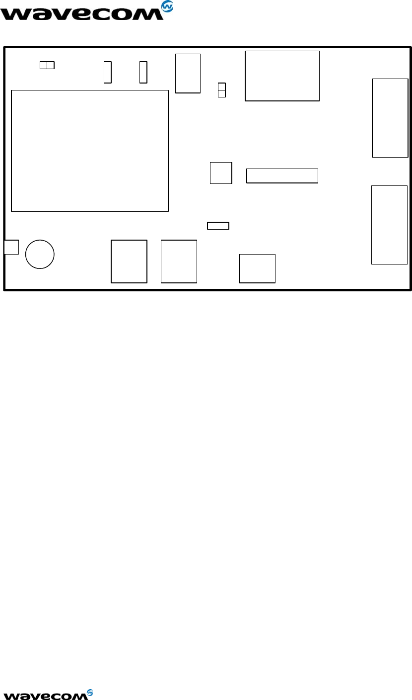
6.1 Layout
The following drawing indicates the relative position of all switches, connectors, and jumpers on the
Interface Board, by functional name.
WM_HWD_SK_UGD_002 - 002
6/1/2005
Confidential © Page: 15 / 18
This document is the sole and exclusive property of WAVECOM. Not to be distributed or divulged without prior written
agreement.
Ce document est la propriété exclusive de WAVECOM. Il ne peut être communiqué ou divulgué à des tiers sans son
autorisation préalable.
MODULE
DM
DB-9 DATA
DB-9
SIM
SOCKET
RF HEADSET HANDSET
HEADSET
JTAG
POWER
INPUT
RESET
SNGL/DIFF
LED 1
VIBRARINGER
OFF/ON
BOOT
LED 2
WM_HWD_SK_UGD_002 - 002
6/1/2005
Confidential © Page: 16 / 18
This document is the sole and exclusive property of WAVECOM. Not to be distributed or divulged without prior written
agreement.
Ce document est la propriété exclusive de WAVECOM. Il ne peut être communiqué ou divulgué à des tiers sans son
autorisation préalable.
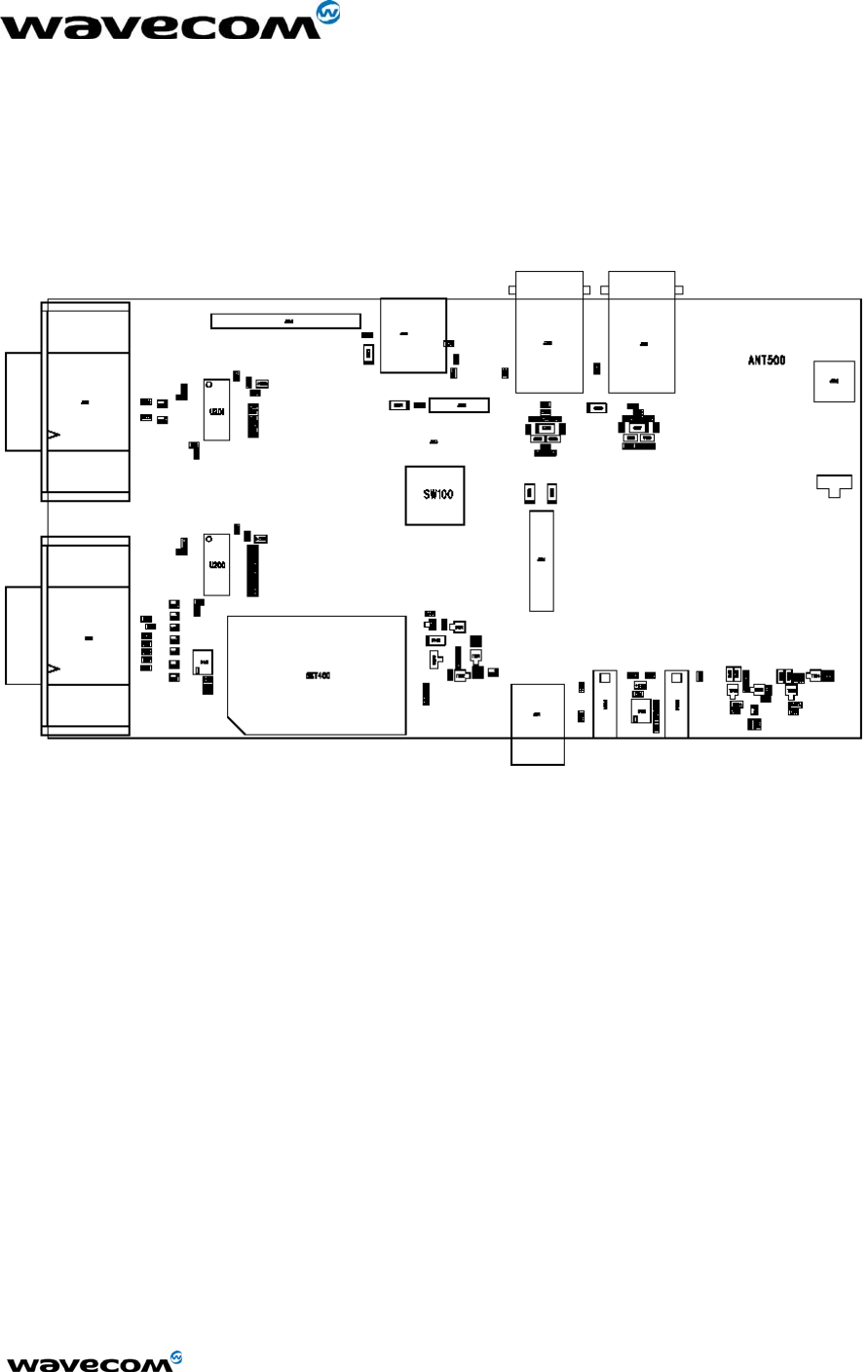
6.2 Assembly Drawing
The following drawing indicates the position of all components on the Interface Board by schematic
reference designator.
WM_HWD_SK_UGD_002 - 002
6/1/2005
Confidential © Page: 17 / 18
This document is the sole and exclusive property of WAVECOM. Not to be distributed or divulged without prior written
agreement.
Ce document est la propriété exclusive de WAVECOM. Il ne peut être communiqué ou divulgué à des tiers sans son
autorisation préalable.
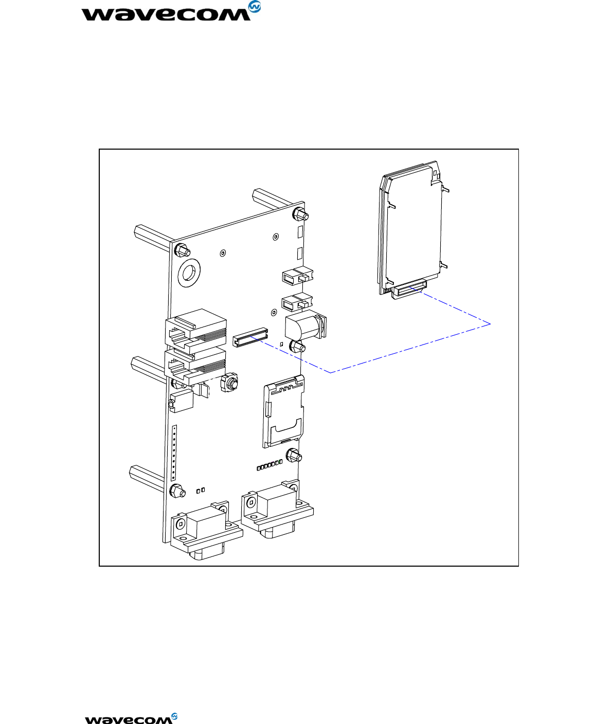
6.3 Isometric
The following drawing is an Isometric drawing of the Interface Board including the Module.

WM_HWD_SK_UGD_002 - 002
6/1/2005
Confidential © Page: 18 / 18
This document is the sole and exclusive property of WAVECOM. Not to be distributed or divulged without prior written
agreement.
Ce document est la propriété exclusive de WAVECOM. Il ne peut être communiqué ou divulgué à des tiers sans son
autorisation préalable.