Sierra Wireless Q2686 Q2686 User Manual Manual
Sierra Wireless, Inc. Q2686 Manual
UserManual.wiki
>
Sierra Wireless
>
Q2686 User Manual
>
Manual
Contents
1.
Manual
2.
Installation Guide
Manual
Navigation menu
Upload a User Manual
Namespaces
Wiki Guide
HTML
PDF
Info
Views
User Manual
Discussion / Help
Navigation
![WM_PRJ_Q2686_PTS_001April 4th 2006confidential ©Page : 12 / 87This document is the sole and exclusive property of WAVECOM. Not to be distributed or divulged without prior written agreement. Ce document est la propriété exclusive de WAVECOM. Il ne peut être communiqué ou divulgué à des tiers sans son autorisation préalable.1References1.1 References documentsFor more details, several references documents can be consulted. The WAVECOM reference documents are provided in the WAVECOM documents package contrary at the general reference documents which are not WAVECOM owner.1.1.1 WAVECOM reference document[1] Automotive Environmental Control Plan for WISMO Quik Q2686 WM_PRJ_Q2686_DCP_001[2] WISMO Quik Q2686 Customer Design GuidelinesWM_PRJ_Q2686_PTS_003[3] WISMO Quik Q2686 Process Customer GuidelinesWM_PRJ_Q2686_PTS_004[4] AT Commands Interface Guide for OS 6.60WM_DEV_OAT_UGD_0031.1.2 General reference document[5] “I²C Bus Specification”, Version 2.0, Philips Semiconductor 1998[6] ISO 7816-3 Standard](https://usermanual.wiki/Sierra-Wireless/Q2686.Manual/User-Guide-652169-Page-12.png)
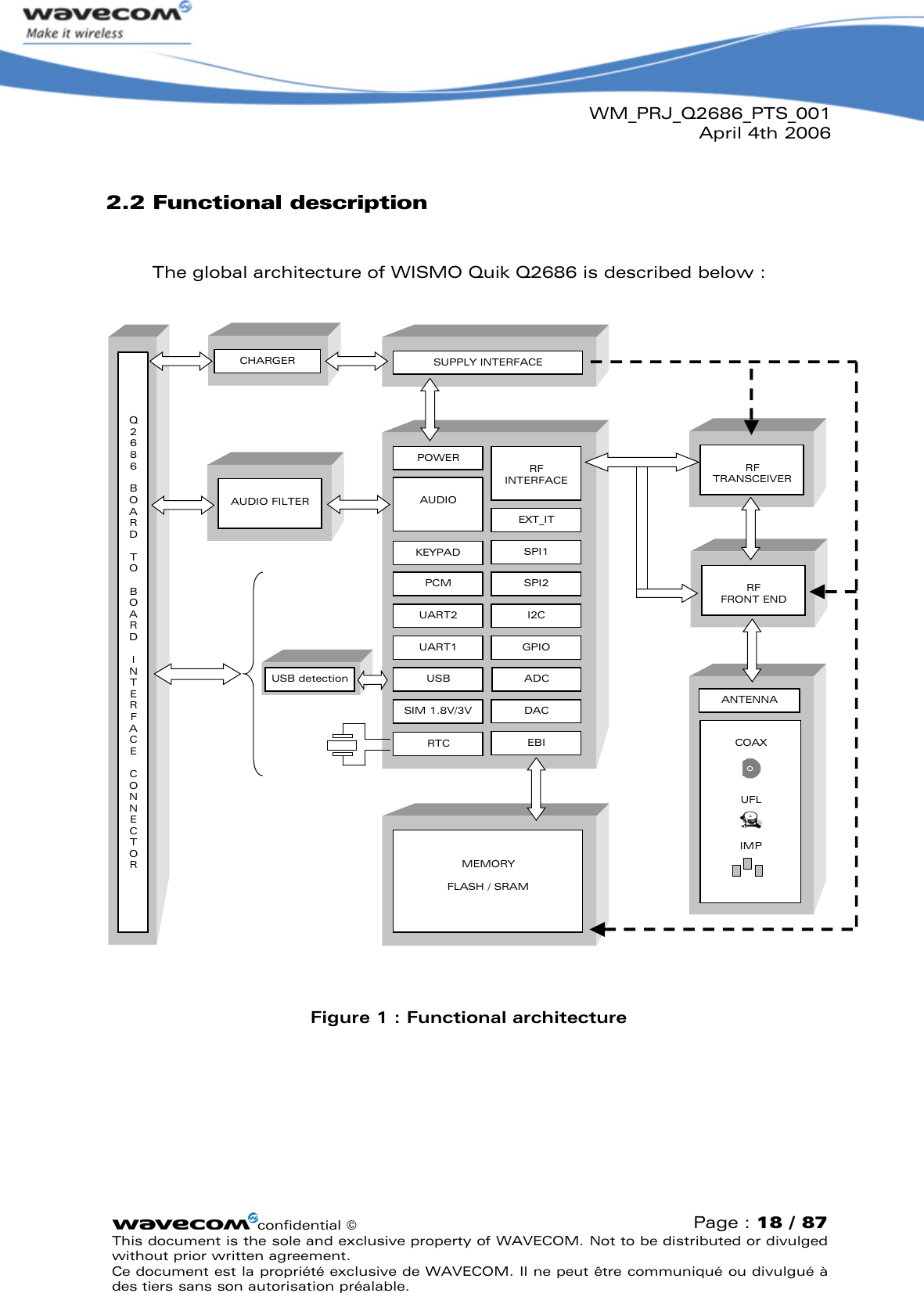
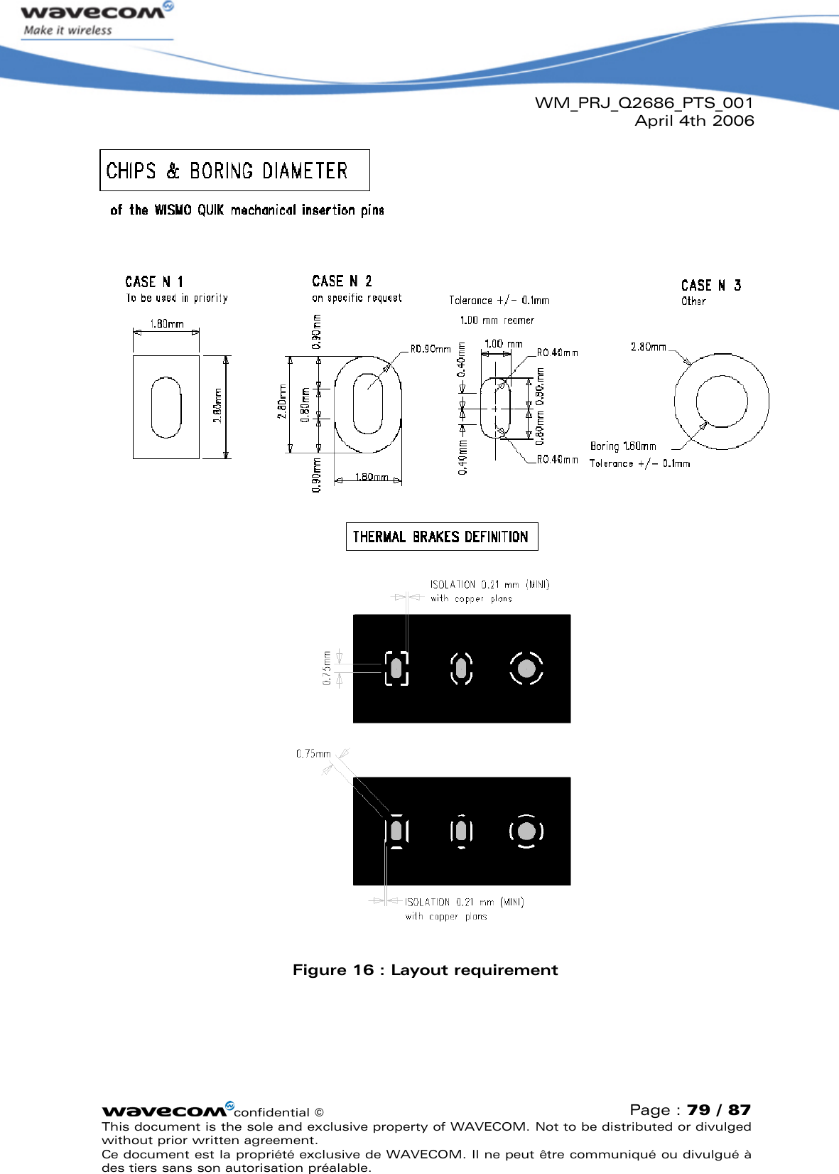
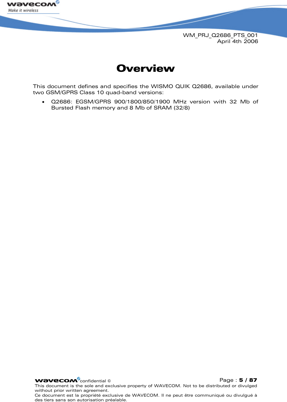
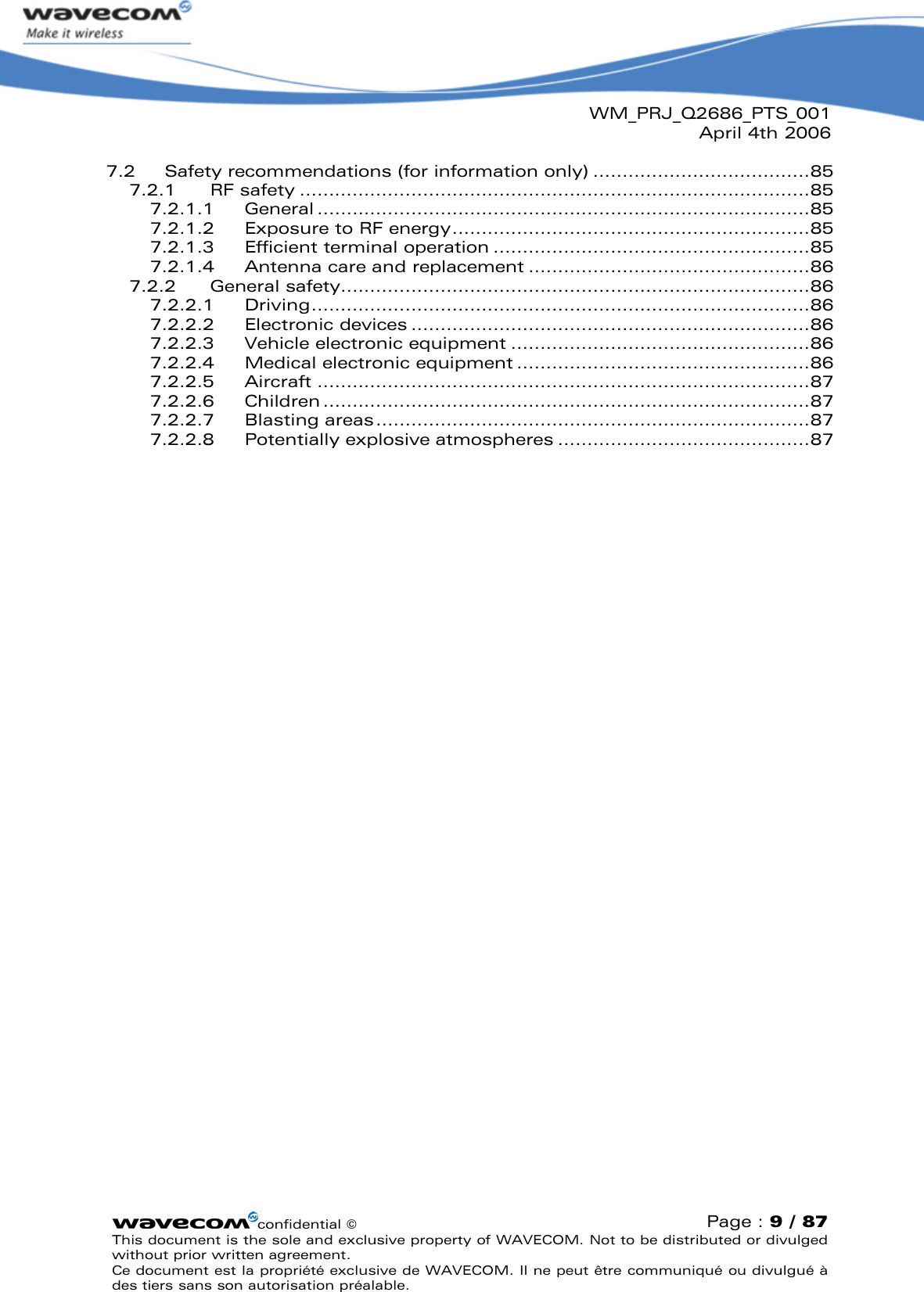
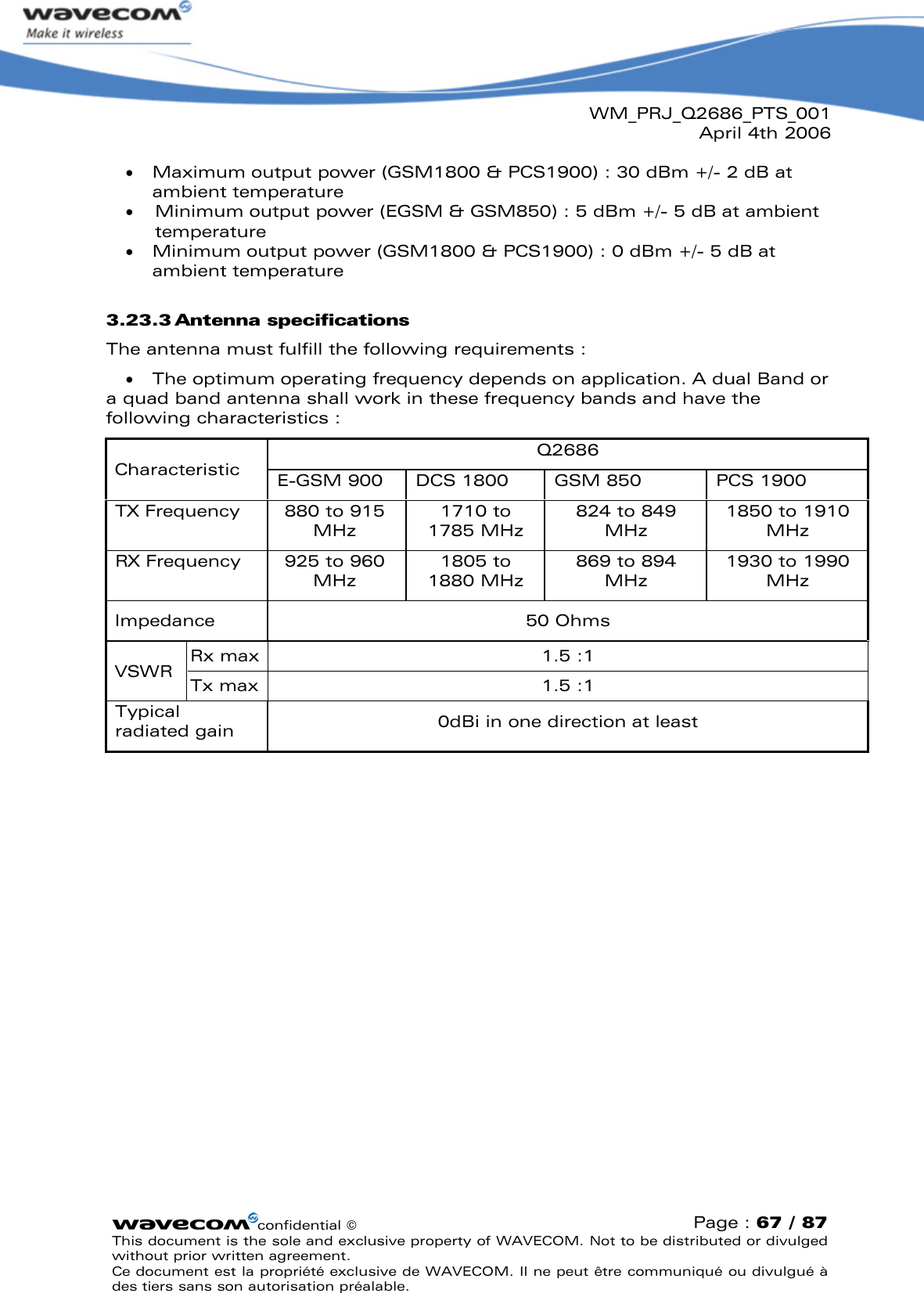
![WM_PRJ_Q2686_PTS_001April 4th 2006confidential ©Page : 22 / 87This document is the sole and exclusive property of WAVECOM. Not to be distributed or divulged without prior written agreement. Ce document est la propriété exclusive de WAVECOM. Il ne peut être communiqué ou divulgué à des tiers sans son autorisation préalable.The WISMO QUIK Q2686 shielding case is the grounding. The ground has to be connected on the mother board through a complete layer on the PCB.Input power Supply VoltageVMIN VNOM VMAX Ripple max (Uripp)VBATT1,2 3.2 3.6 4.8 10mVppTable 1Power supply voltage(1): This value has to be guarantied during the burst (with 2.0A Peak in GSM or GPRS mode)(2): max operating Voltage Stationary Wave Ratio (VSWR) 2:1When supplying the Wireless CPU with a battery, the total impedance (battery+protections+PCB)should be <150 mOhms.When the Wireless CPU is in Alarm mode, no voltage must be applied on any pin of the 100-pin connector excepted on the BAT-RTC (pin 7 ) for RTC operation, or ON/~OFF (pin 19) to power ON the Wireless CPU.3.2.2 Power consumptionThe power consumption is depending of the configuration used. That’s why, the following consumption values are given for each modes, RF bands and software used (AT or Open AT™).All following information are given assuming a 50 RF output.The following consumption values are given by measurement on Wireless CPU samples, at temperature of 25°C.Three VBATT values are used to measure the consumption, VBATTMIN (3.2V), VBATTMAX (4.8V) and VBATTTYP (3.6V). The average current is given for the three VBATT values and the peak current given is the maximal current peak measured with the three VBATT voltages.For more information about working mode description, see Appendix of AT Command Interface Guide OS 6.60 [4]For more information about consumption measurement procedure, see WISMO Quik Q2686 Customer Design Guidelines [2].](https://usermanual.wiki/Sierra-Wireless/Q2686.Manual/User-Guide-652169-Page-22.png)
![WM_PRJ_Q2686_PTS_001April 4th 2006confidential ©Page : 77 / 87This document is the sole and exclusive property of WAVECOM. Not to be distributed or divulged without prior written agreement. Ce document est la propriété exclusive de WAVECOM. Il ne peut être communiqué ou divulgué à des tiers sans son autorisation préalable.6Design GuidelinesThe purpose of the following paragraphs is to give design guidelines. 6.1 HARDWARE and RF6.1.1 EMC recommendationsThe EMC tests have to be performed as soon as possible on the application to detect any possible problem.When designing, special attention should be paid to: Possible spurious emission radiated by the application to the RF receiver in the receiver band ESD protection is mandatory on all signals which have external accessibility ( typically human accessibility ). See WISMO Quik Q2686 Customer Design Guidelines WM_PRJ_Q2686_PTS_003 [2] for ESD protection samples. oTypically ESD protection is mandatory for : SIM (if accessible from outside) serial link,… EMC protection on audio input/output (filters against 900MHz emissions) Biasing of the microphone inputs Length of the SIM interface lines (preferably <10cm) Ground plane : WAVECOM recommends to have a common ground plane for analog / digital / RF grounds. Metallic case or plastic casing with conductive paint are recommendedNote :The Wireless CPU does not include any protection against overvoltage.6.1.2 Power SupplyThe power supply is one of the key issues in the design of a GSM terminal.A weak power supply design could affect in particular : EMC performances the emissions spectrum the phase error and frequency errorWARNING:Careful attention should be paid to :](https://usermanual.wiki/Sierra-Wireless/Q2686.Manual/User-Guide-652169-Page-77.png)