Sierra Wireless Q2686 Cellular GSM/ GPRS Transmitter Module User Manual Q2686 Wireless CPU Product Technical Specification
Sierra Wireless, Inc. Cellular GSM/ GPRS Transmitter Module Q2686 Wireless CPU Product Technical Specification
Contents
- 1. Manual
- 2. Installation Guide
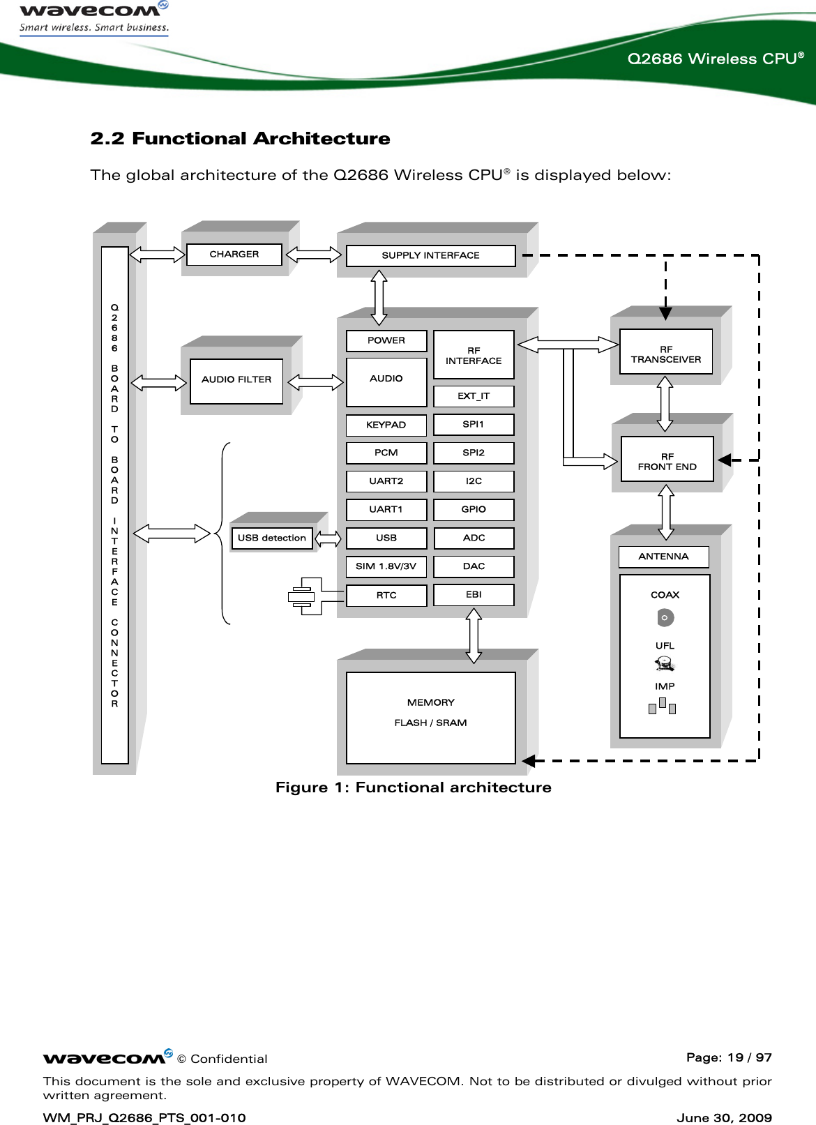
Installation Guide

![© Confidential Page: 13 / 97 This document is the sole and exclusive property of WAVECOM. Not to be distributed or divulged without prior written agreement. WM_PRJ_Q2686_PTS_001-010 June 30, 2009 Q2686 Wireless CPU® 1 References 1.1 Reference Documents For more details, several reference documents may be consulted. The Wavecom reference documents are provided in the Wavecom document package, contrary to the general reference documents which are not authored by Wavecom. Please check the web site for the latest documentation available. Note that the last software version available for Q2686 is Open AT® Software Suite v2.0. 1.1.1 Open AT® Software Documentation [1] Getting started with Open AT® [2] Tutorial for Open AT® [3] Tools Manual for Open AT® [4] Basic Development Guide for Open AT® [5] ADL User Guide for Open AT® [6] Open AT® Release Note 1.1.2 AT Software Documentation [7] AT commands interface Guide V7.1 [8] AT Commands Interface Guide (Bluetooth) [9] Open AT® firmware Release Note 1.1.3 Hardware Documents [10] Q2686 Wireless CPU® Customer Design Guidelines (Ref. WM_PRJ_Q2686_PTS_003) [11] Q2686 Wireless CPU® Process Customer Guidelines (Ref.WM_PRJ_Q2686_PTS_004) 1.1.4 Other Wavecom Documents [12] Automotive Environmental Control Plan for Q2686 Wireless CPU® (Ref. WM_T&D_Q2686_DCP_001) 1.1.5 General Reference Documents [13] “I²C Bus Specification”, Version 2.0, Philips Semiconductor 1998 [14] ISO 7816-3 Standard](https://usermanual.wiki/Sierra-Wireless/Q2686.Installation-Guide/User-Guide-1135580-Page-14.png)
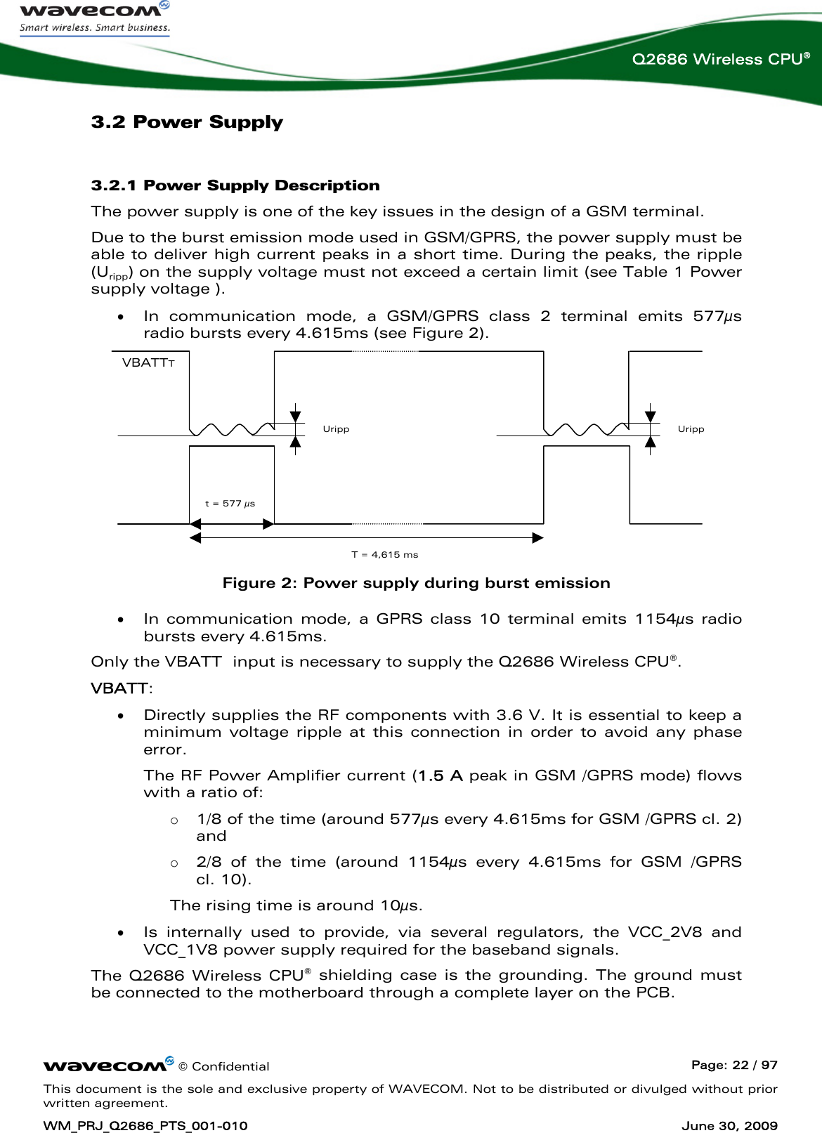
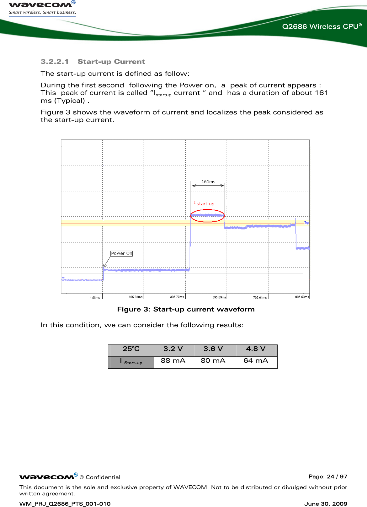
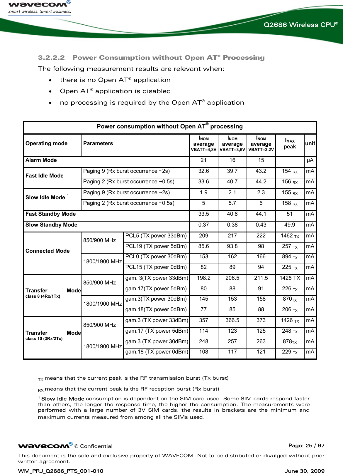
![© Confidential Page: 23 / 97 This document is the sole and exclusive property of WAVECOM. Not to be distributed or divulged without prior written agreement. WM_PRJ_Q2686_PTS_001-010 June 30, 2009 Q2686 Wireless CPU® VMIN VNOM VMAX VBATT1,2 3.2 3.6 4.8 Table 1 Power supply voltage (1): This value must be guarantied during the burst (with 1.5A Peak in GSM or GPRS mode) (2): Max operating Voltage Stationary Wave Ratio (VSWR) 2:1 When the Wireless CPU® is supplied with a battery, the total impedance (battery + protections + PCB) should be < 150 mΩ. As the radio power amplifier is directly connected to VBATT, the Wireless CPU® is sensitive to any Alternative Current on lines. When a DC/DC converter is used, Wavecom recommends setting the converter frequency in such a way that the resulting voltage does not exceed the values in following table. Freq. (kHz) Uripp Max (mVpp) <10 300 10 ≤ f ≤ 200 40 > 200 10 Table 2 Maximum voltage ripple (Uripp) vs Frequency When the Wireless CPU® is in Alarm/Off mode, no voltage has to be applied on any pin of the 100-pin connector, except on Vbatt (pins 1 to 4) ,BAT-RTC (pin 7) for RTC operation or ON/~OFF (pin 19) to power-ON the Wireless CPU®. 3.2.2 Power Consumption Power consumption is dependent on the configuration used. It is for this reason that the following consumption values are given for each mode, RF band and type of software used (AT or Open AT®). All the following information is given assuming a 50 Ω RF output. The following consumption values were obtained by performing measurements on the Wireless CPU® samples at a temperature of 25° C. Three VBATT values are used to measure the consumption, VBATTMIN (3.2V), VBATTMAX (4.8V) and VBATTTYP (3.6V). The average current is given for the three VBATT values and the peak current given is the maximum current peak measured with the three VBATT voltages. For a more detailed description of the operating modes, see the appendix of the AT Command User Guide [7]. For more information on the consumption measurement procedure, see Q2686 Wireless CPU® Customer Design Guidelines [10]. First let’s define start-up current in view to avoid start issues.](https://usermanual.wiki/Sierra-Wireless/Q2686.Installation-Guide/User-Guide-1135580-Page-24.png)
![© Confidential Page: 36 / 97 This document is the sole and exclusive property of WAVECOM. Not to be distributed or divulged without prior written agreement. WM_PRJ_Q2686_PTS_001-010 June 30, 2009 Q2686 Wireless CPU® 3.4.2 I2C Bus The I2C interface includes a clock signal (SCL1) and data signal (SDA1) complying with a 100kbit/s-standard interface (standard mode: s-mode). The I²C bus is always master. The maximum speed transfer range is 400kbit/s (fast mode: f-mode). For more information on the bus, see the “I²C Bus Specification Version 2.0” from PHILIPS [13]. 3.4.2.1 I²C Waveforms I²C bus waveform in master mode configuration: Figure 6: I²C Timing diagrams, Master AC characteristics Signal Description Minimum Typ Maximum Unit SCL1-freq I²C clock frequency 100 400 kHz T-start Hold time START condition 0.6 μs T-stop Setup time STOP condition 0.6 μs T-free Bus free time, STOP to START 1.3 μs T-high High period for clock 0.6 μs T-data-hold Data hold time 0 0.9 μs T-data-setup Data setup time 100 ns](https://usermanual.wiki/Sierra-Wireless/Q2686.Installation-Guide/User-Guide-1135580-Page-37.png)
![© Confidential Page: 39 / 97 This document is the sole and exclusive property of WAVECOM. Not to be distributed or divulged without prior written agreement. WM_PRJ_Q2686_PTS_001-010 June 30, 2009 Q2686 Wireless CPU® The rise and fall time of the reception signals (mainly CT103) must be less than 300 ns. The maximum baud rate of UART1 is 921 kbit/s for the firmware provided in the Open AT® Software Suite v2. Recommendation: The Q2686 Wireless CPU® is designed to operate using all the serial interface signals. In particular, it is recommended to use RTS and CTS for hardware flow control in order to avoid data loss during transmission. For use with 5-wire serial interface • Signal: CT103/TXD1*, CT104/RXD1*, ~CT105/RTS1*, ~CT106/CTS1* • The signal ~CT108-2/DTR1* must be managed by following the V24 protocol signalling, if you want to use the slow idle mode. • Other signals and their multiplexes are not available. • Please refer to technical appendixes of AT commands User Guide [7] for more information. For use with 4-wire serial interface • CT103/TXD1*, CT104/RXD1*, ~CT105/RTS1*, ~CT106/CTS1* • The signal ~CT108-2/DTR1* must be configured at low level. • Other signals and their multiplexes are not available. • Please refer to technical appendixes in the AT commands User Guide [7] for more information. For use with 2-wire serial interface • This case is possible for connected external chip, but not recommended (and forbidden for AT command or modem use) • The flow control mechanism has to be managed at the customer side. • CT103/TXD1*, CT104/RXD1* • The signal ~CT108-2/DTR1* must be configured at low level. • The signals ~CT105/RTS1*, ~CT106/CTS1* are not used, please configure the AT command (AT+IFC=0,0 see AT command User Guide [7]). • The signal ~CT105/RTS1* must be configured at low level. • Other signals and their multiplexes are not available. • Please refer to technical appendixes in the AT commands User Guide [7] for more information.](https://usermanual.wiki/Sierra-Wireless/Q2686.Installation-Guide/User-Guide-1135580-Page-40.png)
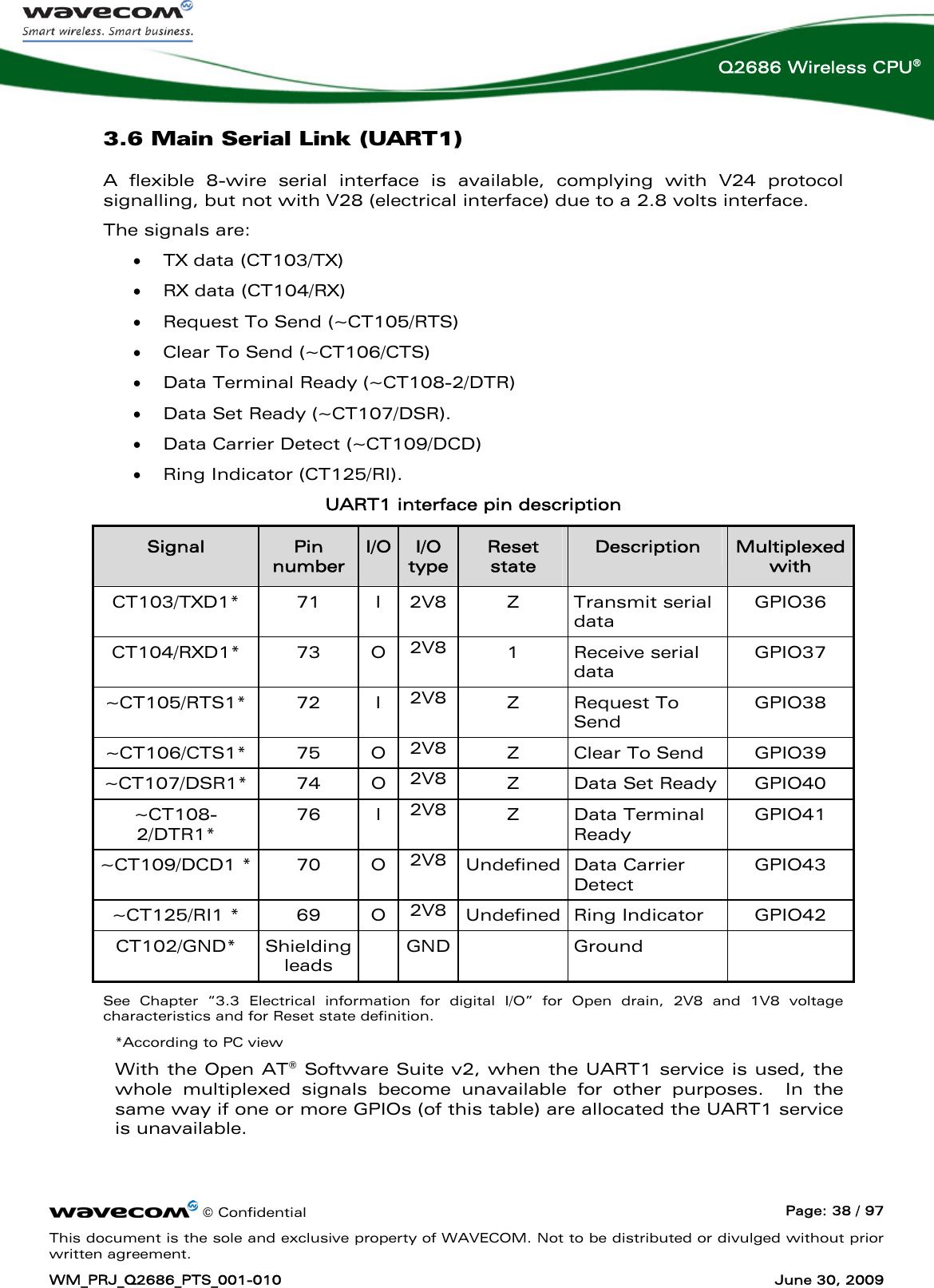
![© Confidential Page: 40 / 97 This document is the sole and exclusive property of WAVECOM. Not to be distributed or divulged without prior written agreement. WM_PRJ_Q2686_PTS_001-010 June 30, 2009 Q2686 Wireless CPU® 3.7 Auxiliary Serial Link (UART2) An auxiliary serial interface (UART2) is available on Q2686. This interface may be used to connect a Bluetooth or a GPS chip controlled by an Open AT® Plug-in. UART2 interface pin description Signal Pin number I/O I/O type Reset state Description Multiplexed with CT103 / TXD2* 31 I 1V8 Z Transmit serial data GPIO14 CT104 / RXD2* 30 O 1V8 Z Receive serial data GPIO15 ~CT106 / CTS2* 32 O 1V8 Z Clear To Send GPIO16 ~CT105 / RTS2* 33 I 1V8 Z Request To Send GPIO17 See Chapter 3.3, “Electrical information for digital I/O” for Open drain, 2V8 and 1V8 voltage characteristics and Reset state definition. * According to PC view The Q2686 is designed to operate using all the serial interface signals. In particular, it is recommended to use RTS and CTS for hardware flow control in order to avoid data corruption during transmission. The maximum baud rate of UART2 is 921 kbit/s for the firmware provided with Open AT® Software Suite v2. For use with 4-wire serial interface • CT103/TXD2*, CT104/RXD2*, ~CT105/RTS2*, ~CT106/CTS2* • The signal ~CT108-2/DTR2* must be configured at low level. • Other signals and their multiplexes are not available. • Please refer to technical appendixes in the AT commands User Guide [7] for more information. For use with 2-wire serial interface • This case is possible for connected external chip, but not recommended (and forbidden for AT command or modem use) • The flow control mechanism has to be managed at the customer side. • CT103/TXD2*, CT104/RXD2* • The signals ~CT105/RTS2*, ~CT106/CTS2* are not used, you must configure the AT command (AT+IFC=0,0 see AT commands User Guide [7]).](https://usermanual.wiki/Sierra-Wireless/Q2686.Installation-Guide/User-Guide-1135580-Page-41.png)
![© Confidential Page: 41 / 97 This document is the sole and exclusive property of WAVECOM. Not to be distributed or divulged without prior written agreement. WM_PRJ_Q2686_PTS_001-010 June 30, 2009 Q2686 Wireless CPU® • The signal ~CT105/RTS2* must be configured at low level. • Other signals and their multiplexes are not available. • Please refer to technical appendixes in the AT commands User Guide [7] for more information. 3.8 SIM Interface The Subscriber Identification Module (SIM) may be directly connected to the Q2686 Wireless CPU® via this dedicated interface. 3.8.1 General Description The five signals are: • SIM-VCC: SIM power supply • ~SIM-RST: reset • SIM-CLK: clock • SIM-IO: I/O port • SIMPRES: SIM card detect The SIM interface controls a 3V/1V8 SIM. This interface is fully compliant with the GSM 11.11 recommendations concerning SIM functions. SIM interface pin description Signal Pin number I/O I/O type Reset state Description Multiplexed with SIM-CLK 14 O 2V9 / 1V8 0 SIM Clock Not mux ~SIM-RST 13 O 2V9 / 1V8 0 SIM Reset Not mux SIM-IO 11 I/O 2V9 / 1V8 *Pull-up SIM Data Not mux SIM-VCC 9 O 2V9 / 1V8 SIM Power Supply Not mux SIMPRES 12 I 1V8 Z SIM Card Detect GPIO18 *SIM-IO pull-up is about 10 k Ω. See Chapter 3.3 “Electrical information for digital I/O” for Open drain, 2V8 and 1V8 voltage characteristics and Reset state definition.](https://usermanual.wiki/Sierra-Wireless/Q2686.Installation-Guide/User-Guide-1135580-Page-42.png)
![© Confidential Page: 44 / 97 This document is the sole and exclusive property of WAVECOM. Not to be distributed or divulged without prior written agreement. WM_PRJ_Q2686_PTS_001-010 June 30, 2009 Q2686 Wireless CPU® Signal Pin number I/O I/O type* Reset state Multiplexed with GPIO24 58 I/O 2V8 Z Not mux GPIO25 49 I/O 2V8 Z INT1 GPIO26 44 I/O Open drain Z SCL1 GPIO27 46 I/O Open drain Z SDA1 GPIO28 23 I/O 2V8 Z SPI1-CLK GPIO29 25 I/O 2V8 Z SPI1-IO GPIO30 24 I/O 2V8 Z SP1-I GPIO31 22 I/O 2V8 Z GPIO32 26 I/O 2V8 Z SPI2-CLK GPIO33 27 I/O 2V8 Z SPI2-IO GPIO34 29 I/O 2V8 Z SP2-I GPIO35 28 I/O 2V8 Z GPIO36 71 I/O 2V8 Z CT103 / TXD1 GPIO37 73 I/O 2V8 1 CT104 / RXD1 GPIO38 72 I/O 2V8 Z ~CT105 / RTS1 GPIO39 75 I/O 2V8 Z ~CT106 / CTS1 GPIO40 74 I/O 2V8 Z ~CT107 / DSR1 GPIO41 76 I/O 2V8 Z ~CT108-2 / DTR1 GPIO42 69 I/O 2V8 Undefined ~CT125 / RI1 GPIO43 70 I/O 2V8 Undefined ~CT109 / DCD1 See Chapter 3.3, “Electrical information for digital I/O” for Open drain, 2V8 and 1V8 voltage characteristics and Reset state definition. * If a Bluetooth module is used with the Q2686 Wireless CPU®, these GPIOs must be reserved. ** With the Open AT® Software Suite v2: see “AT commands User Guide ” [7].](https://usermanual.wiki/Sierra-Wireless/Q2686.Installation-Guide/User-Guide-1135580-Page-45.png)
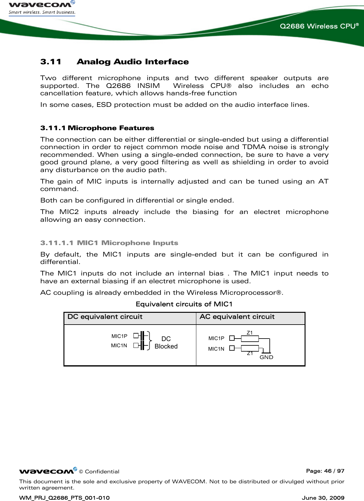
![© Confidential Page: 47 / 97 This document is the sole and exclusive property of WAVECOM. Not to be distributed or divulged without prior written agreement. WM_PRJ_Q2686_PTS_001-010 June 30, 2009 Q2686 Wireless CPU® Electrical Characteristics of MIC1 Parameters Min Typ Max Unit DC Characteristics N/A V AC Characteristics 200 Hz<F<4 kHz Z1 70 120 160 kΩ AT+VGT*=3500(4) 13.8 18.6*** mVrms AT+VGT*=2000(4) 77.5 104*** mVrms Working voltage ( MIC1P-MIC1N) AT+VGT*=700(4) 346 465*** mVrms Positive +7.35 V Maximum rating voltage (MIC1P or MIC1N) Negative -0.9 • *The input voltage depends of the input micro gain set by AT command. Please refer to the document :AT command User Guide [7] • **Because MIC2P is internally biased, it is necessary to use a coupling capacitor to connect an audio signal provided by an active generator. Only a passive microphone can be directly connected to the MIC2P and MIC2N inputs. • *** This value is obtained with digital gain = 0 and for frequency = 1kHz : • (4) This value is given in dB, but it’s possible to toggle to index value. Please refer to the document :AT command User Guide [7] WARNING: The voltage input value for MIC1 can’t exceed the maximum working voltage, otherwise clipping will appear. 3.11.1.2 MIC2 Microphone Inputs By default, the MIC2 inputs are differential ones, but it can be configured in single ended. They already include the convenient biasing for an electret microphone. The electret microphone can be directly connected on those inputs, thus allowing easy connection to a handset. AC coupling is already embedded in the Wireless CPU®. Equivalent circuits of MIC2 DC equivalent circuit AC equivalent circuit MIC2P MIC2N Z2 Z2 GND MIC2+ MIC2P MIC2N RRGND](https://usermanual.wiki/Sierra-Wireless/Q2686.Installation-Guide/User-Guide-1135580-Page-48.png)
![© Confidential Page: 48 / 97 This document is the sole and exclusive property of WAVECOM. Not to be distributed or divulged without prior written agreement. WM_PRJ_Q2686_PTS_001-010 June 30, 2009 Q2686 Wireless CPU® Electrical Characteristics of MIC2 Parameters Min Typ Max Unit MIC2+ 2 2.1 2.2 V Output current 0.5 1.5 mA Internal biasing DC Characteristics R2 1650 1900 2150 Ω Z2 MIC2P (MIC2N=Open) Z2 MIC2N (MIC2P=Open) 1.1 1.3 1.6 Z2 MIC2P (MIC2N=GND) Z2 MIC2N (MIC2P=GND) 0.9 1.1 1.4 AC Characteristics 200 Hz<F<4 kHz Impedance between MIC2P and MIC2N 1.3 1.6 2 kΩ AT+VGT*=3500(4) 13.8 18.6 *** AT+VGT*=2000(4) 77.5 104*** Working voltage ( MIC2P-MIC2N) AT+VGT*=700(4) 346 466*** mVrms Positive +7.35** Maximum rating voltage (MIC2P or MIC2N) Negative -0.9 V • *The input voltage depends of the input micro gain set by AT command. Please refer to the document : AT command User Guide[7] • **Because MIC2P is internally biased, it is necessary to use a coupling capacitor to connect an audio signal provided by an active generator. Only a passive microphone can be directly connected to the MIC2P and MIC2N inputs. • *** This value is obtained with digital gain = 0 and for frequency = 1kHz .. • (4) This value is given in dB, but it’s possible to toggle to index value. Please refer to the document :AT command User Guide [7] WARNING: The voltage input value for MIC2 can’t exceed the maximum working voltage, otherwise clipping will appear.](https://usermanual.wiki/Sierra-Wireless/Q2686.Installation-Guide/User-Guide-1135580-Page-49.png)
![© Confidential Page: 50 / 97 This document is the sole and exclusive property of WAVECOM. Not to be distributed or divulged without prior written agreement. WM_PRJ_Q2686_PTS_001-010 June 30, 2009 Q2686 Wireless CPU® Electrical Characteristics of SPK1 Parameters Min Typ Max Unit Biasing voltage - 1.30 V RL=16Ω: AT+VGR=-1600**; single-ended - 1.7 - Vpp Output swing voltage RL=32Ω; AT+VGR=-1600**; single-ended - 1.9 2.75 Vpp RL Load resistance 14.5 32 - Ω RL=16Ω - 40 85 mA IOUT Output current; single-ended; peak value RL=32Ω - 22 - mA RL=16Ω; AT+VGR*=-1600** - 25 mW POUT RL=32Ω; AT+VGR*=-1600** - 16 27 mW RPD Output pull-down resistance at power-down 28 40 52 kΩ • *The output voltage depends of the output speaker gain set by AT command. Please refer to the document AT command User Guide [7]. • ** This value is given in dB, but it’s possible to toggle to index value. Please refer to the document :AT command User Guide [7] 3.11.2.1.2 SPK2 Speaker Outputs The SPK2 interface allows differential and single ended speaker connection Equivalent circuits of SPK2](https://usermanual.wiki/Sierra-Wireless/Q2686.Installation-Guide/User-Guide-1135580-Page-51.png)
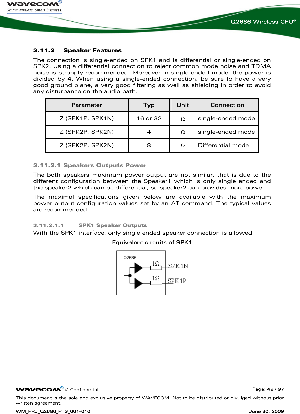
![© Confidential Page: 51 / 97 This document is the sole and exclusive property of WAVECOM. Not to be distributed or divulged without prior written agreement. WM_PRJ_Q2686_PTS_001-010 June 30, 2009 Q2686 Wireless CPU® Electrical Characteristics of SPK2 Parameters Min Typ Max Unit Biasing voltage SPK2P and SPK2N 1.30 V RL=8Ω: AT+VGR=-1000*; single ended - - 2 Vpp RL=8Ω: AT+VGR=-1000*; differential - - 4 Vpp RL=32Ω: AT+VGR=-1000*; single ended - - 2.5 Vpp Output swing voltage RL=32Ω: AT+VGR=-1000*; differential - - 5 Vpp RL Load resistance 6 8 - Ω IOUT Output current; peak value; RL=8Ω - - 180 mA POUT RL=8Ω; AT+VGR=-1000*; - - 250 mW RPD Output pull-down resistance at power-down 28 40 52 kΩ VPD Output DC voltage at power-down - - 100 mV • *The output voltage depends of the output speaker gain set by AT command. Please refer to the document: AT command User Guide [7].This value is given in dB, but it’s possible to toggle to index value. If a singled ended solution is used with the speaker2 output, only one of the both SPK2 has to be chosen. The result is a maximal output power divided by 4. 3.11.3 Pin description Signal Pin number I/O I/O type Description MIC1P 40 I Analog Microphone 1 positive input MIC1N 38 I Analog Microphone 1 negative input MIC2P 36 I Analog Microphone 2 positive input MIC2N 34 I Analog Microphone 2 negative input SPK1P 35 O Analog Speaker 1 positive output SPK1N 37 O Analog Speaker 1 negative output SPK2P 39 O Analog Speaker 2 positive output SPK2N 41 O Analog Speaker 2 negative output](https://usermanual.wiki/Sierra-Wireless/Q2686.Installation-Guide/User-Guide-1135580-Page-52.png)

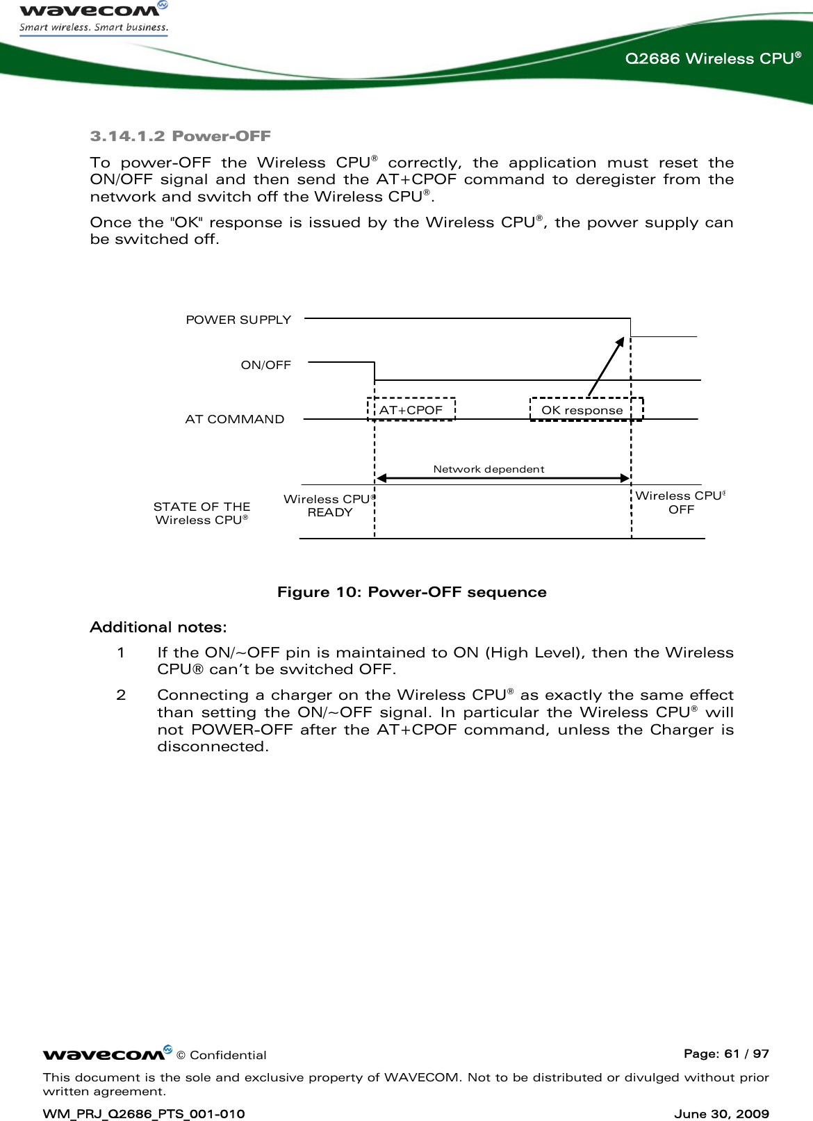
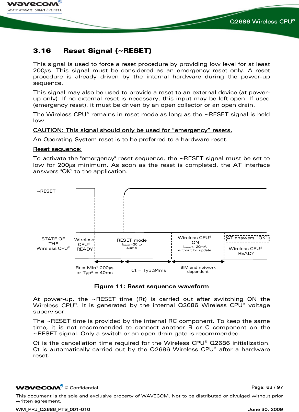
![© Confidential Page: 58 / 97 This document is the sole and exclusive property of WAVECOM. Not to be distributed or divulged without prior written agreement. WM_PRJ_Q2686_PTS_001-010 June 30, 2009 Q2686 Wireless CPU® 3.14 ON / ~OFF signal This input is used to switch the Q2686 Wireless CPU® ON or OFF. A high-level signal must be provided on the ON/~OFF pin to switch ON the Wireless CPU®. The voltage of this signal has to be maintained higher than 0.8 x VBATT during a minimum of 1500ms. This signal can be left at high level until switch-off. To switch OFF the Wireless CPU®, the ON/OFF pin must be released. The Wireless CPU® can be switched off via the Operating System. Pin description Signal Pin number I/O I/O type Description ON/∼OFF 19 I CMOS Wireless CPU® Power-ON Electrical characteristics of the signals Parameter I/O type Minimum Maximum Unit VIL CMOS VBATT x 0.2 V VIH CMOS VBATT x 0.8 VBATT V Warning: All external signals must be inactive when the Wireless CPU® is OFF to avoid any damage when starting and allow the Wireless CPU® to start and stop correctly. 3.14.1 Operating Sequences 3.14.1.1 Power-ON Once the Wireless CPU® is supplied, the application must set the ON/OFF signal to high to start the Wireless CPU® power-ON sequence. The ON/OFF signal must be held high during a minimum delay of Ton/off-hold (Minimum hold delay on the ON/~OFF signal) to power-ON. After this delay, an internal mechanism maintains the Wireless CPU® in power-ON condition. During the power-ON sequence, an internal reset is automatically performed by the Wireless CPU® for 40ms (typical). Any external reset should be avoided during this phase. Once initialization is completed (timing is SIM- and network-dependent), the AT interface answers "OK" to the application. For further details, please check the AT Commands User Guide [7].](https://usermanual.wiki/Sierra-Wireless/Q2686.Installation-Guide/User-Guide-1135580-Page-59.png)
![© Confidential Page: 59 / 97 This document is the sole and exclusive property of WAVECOM. Not to be distributed or divulged without prior written agreement. WM_PRJ_Q2686_PTS_001-010 June 30, 2009 Q2686 Wireless CPU® POWER SUPPLY ON/OFF STATE OF THE Wireless CPU ® Wireless CPU ® OFF IBB+RF < 22μA AT answers « OK » Wireless CPU ® READY Ton/off-hold (2000ms min) SIM and Network dependent RESET mode IBB+RF=20 to 40mAINTERNAL RST Trst (40ms typ) Wireless CPU ® ON IBB+RF<120mA IBB+RF = overall current consumption (Base Band + RF part) Figure 9: Power-ON sequence (no PIN code activated) The duration of the firmware power-up sequence depends on: • the need to perform a recovery sequence if the power has been lost during a flash memory modification. Other factors have a minor influence • the number of parameters stored in EEPROM by the AT commands received so far • the ageing of the hardware components, especially the flash memory • the temperature conditions The recommended way to de-assert the ON/~OFF signal is to use either an AT command or WIND indicators: the application must detect the end of the power-up initialization and de-assert ON/~OFF afterwards. • Send an “AT” command and wait for the “OK” answer: once the initialization is complete the AT interface answers « OK » to “AT” message1. • Wait for the “+WIND: 3” message: after initialization, the Wireless CPU®, if configured to do so, will return an unsolicited “+WIND: 3” message. The generation of this message is enabled or disabled via an AT command. Note: See also “AT Commands User Guide” [7] for more information on these commands. 1 If the application manages hardware flow control, the AT command can be sent during the initialisation phase.](https://usermanual.wiki/Sierra-Wireless/Q2686.Installation-Guide/User-Guide-1135580-Page-60.png)
![© Confidential Page: 62 / 97 This document is the sole and exclusive property of WAVECOM. Not to be distributed or divulged without prior written agreement. WM_PRJ_Q2686_PTS_001-010 June 30, 2009 Q2686 Wireless CPU® 3.15 BOOT Signal A specific BOOT control pin is available to download the Q2686 Wireless CPU® (only if the standard XModem download, controlled with AT command, is not possible). A specific PC software program, provided by Wavecom, is needed to perform this specific download. The BOOT pin must be connected to VCC_1V8 for this specific download. Operating mode description BOOT Operating mode Comment Leave open Normal use No download Leave open Download XModem AT command for Download AT+WDWL 1 Download specific Need Wavecom PC software For more information, see Q2686 / Open AT® Software Suite v2 AT Command User Guide [7]. This BOOT pin must be left open either for normal use or XModem download. However, in order to render the development and maintenance phases easier, it is highly recommended to set a test point, either a jumper or a switch on the VCC_1V8 (pin 5) power supply. Pin description Signal Pin number I/O I/O type Description BOOT 16 I 1V8 Download mode selection](https://usermanual.wiki/Sierra-Wireless/Q2686.Installation-Guide/User-Guide-1135580-Page-63.png)


![© Confidential Page: 81 / 97 This document is the sole and exclusive property of WAVECOM. Not to be distributed or divulged without prior written agreement. WM_PRJ_Q2686_PTS_001-010 June 30, 2009 Q2686 Wireless CPU® 4.2 Labeling Correspondence between Q2686 and Open AT® Software Suite v2 Each signal has strictly the same characteristics: It is only a new designation in view to conform with the AT Command User Guide [7]. Signal Name Q2686 with SW preceding Open AT® Software Suite v2 Signal Name Q2686 with SW from Open AT® Software Suite v2 Description I/O PIN number +VBATT ADC0 / +VBATT Possibility to read VBATT value using the ADC0 I 1,2,2,4 BAT-TEMP ADC1/BAT-TEMP Possibility to read either the Battery’s temperature or something else customer specific I 20 AUX-ADC ADC2 Analog to Digital converter I 21 SCL SCL1 O 44 SDA SDA1 I/O 46 FLASHLED LED0 O 17 ~SPI1_CS GPIO31 / SPI1 Load O 22 ~SPI2_CS GPIO35 / SPI2-Load O 28 BUZZ-OUT BUZZER0 O 15 GPIO44 GPIO0 I/O 43](https://usermanual.wiki/Sierra-Wireless/Q2686.Installation-Guide/User-Guide-1135580-Page-82.png)
![© Confidential Page: 87 / 97 This document is the sole and exclusive property of WAVECOM. Not to be distributed or divulged without prior written agreement. WM_PRJ_Q2686_PTS_001-010 June 30, 2009 Q2686 Wireless CPU® 6 Design Guidelines The purpose of the following paragraphs is to give design guidelines. 6.1 HARDWARE and RF 6.1.1 EMC Recommendations The EMC tests must be performed on the application as soon as possible to detect any potential problems. When designing, special attention should be paid to: • Possible spurious emission radiated by the application to the RF receiver in the receiver band • ESD protection is mandatory on all signals which have external accessibility (typically human accessibility). See Q2686 Wireless CPU® Customer Design Guidelines WM_PRJ_Q2686_PTS_003 [10] for ESD protection samples. o Typically, ESD protection is mandatory for the: SIM (if accessible from outside) Serial link • EMC protection on audio input/output (filters against 900MHz emissions) • Biasing of the microphone inputs • Length of the SIM interface lines (preferably <10cm) • Ground plane: Wavecom recommends a common ground plane for analog/digital/RF grounds. • A metallic case or plastic casing with conductive paint are recommended Note: The Wireless CPU® does not include any protection against over-voltage.](https://usermanual.wiki/Sierra-Wireless/Q2686.Installation-Guide/User-Guide-1135580-Page-88.png)
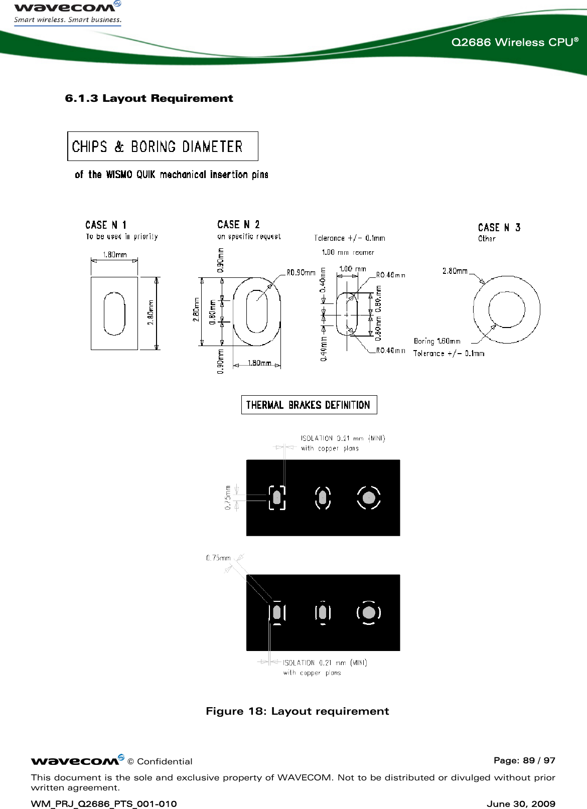
![© Confidential Page: 90 / 97 This document is the sole and exclusive property of WAVECOM. Not to be distributed or divulged without prior written agreement. WM_PRJ_Q2686_PTS_001-010 June 30, 2009 Q2686 Wireless CPU® 6.1.4 Antenna WARNING: Wavecom strongly recommends working with an antenna manufacturer either to develop an antenna adapted to the application or to adapt an existing solution to the application. Both the mechanical and electrical antenna adaptation is one of the key issues in the design of the GSM terminal. 6.2 Mechanical Integration Attention should be paid to: • Antenna cable integration (bending, length, position, etc) • Leads of the Wireless CPU® to be soldered to the Ground plane 6.3 Operating System Upgrade The Q2686 Wireless CPU® Operating System is stored in flash memory and can easily be upgraded. IMPORTANT: In order to follow regular changes in the GPRS standard and to offer a state-of-the-art Operating System, Wavecom recommends that the application designed around a Wireless CPU® (or Wireless CPU® based product) allow easy Operating System upgrades on the Wireless CPU® via the standard X-modem protocol. Therefore, the application shall either allow a direct access to the Wireless CPU® serial link through an external connector or implement any mechanism allowing the Wireless CPU® Operating System to be downloaded via X-modem. The Operating System file can be downloaded to the modem using the X-modem protocol. The AT+WDWL command allows the download process to be launched (see the description in the AT Command User Guide [7]). The serial signals required to proceed with X-modem downloading are: Rx, Tx, RTS, CTS and GND. The Operating System file can also be downloaded to the modem using the DOTA (download over the air) feature. This feature is available with the Open AT® interface. For more details, please, refer to the Open AT® documentation listed in section 1.1.1.](https://usermanual.wiki/Sierra-Wireless/Q2686.Installation-Guide/User-Guide-1135580-Page-91.png)
![WAVECOM S.A. : 3 esplanade du Foncet - 92442 Issy-les-Moulineaux - France - Tel: +33 1 46 29 08 00 - Fax: +33 1 46 29 08 08Wavecom, Inc: 430 Davis Drive, Suite 300 Research Triangle Park, North Carolina, USA - Tel: +1 919 237 4000 - Fax: +1 919 237 4140WAVECOM Asia-Pacific: Unit 201-207, 2nd Floor, Bio-Informatics Centre No. 2 Science Park West Avenue, Hong Kong Science Park,Shatin, New Territories, Hong Kong (PRC) - Tel: +852-2824 0254 - Fax: +852-2824 0255 [Online contact details, GPS and maps]](https://usermanual.wiki/Sierra-Wireless/Q2686.Installation-Guide/User-Guide-1135580-Page-99.png)