Sierra Wireless Q26ELITE Cellular/ PCS CDMA Transmitter Module User Manual Q26 Elite Wireless CPU Product Manual
Sierra Wireless, Inc. Cellular/ PCS CDMA Transmitter Module Q26 Elite Wireless CPU Product Manual
Users Manual

Revision: 002
Date: April 17, 2009
Reference: WI_DEV_Q26EL_UGD_002
Q26 Elite Wireless CPU®
Product Manual

© Confidential Page: 1 / 18
This document is the sole and exclusive property of WAVECOM. Not to be distributed or divulged without prior
written agreement.
WI_DEV_Q26EL_UGD_002-002 April 17, 2009
Q26 Elite User Manual
Q26 Elite Wireless CPU®
User Manual
Reference:
WI_DEV_Q26EL_UGD_002
Revision:
002
Date:
April 17, 2009
© Confidential Page: 2 / 18
This document is the sole and exclusive property of WAVECOM. Not to be distributed or divulged without prior
written agreement.
WI_DEV_Q26EL_UGD_002-002 April 17, 2009
Q26 Elite User Manual
Document History
Revision Date List of revisions
001 April 7, 2009 Creation
002 April 17, 2009 Updates

© Confidential Page: 3 / 18
This document is the sole and exclusive property of WAVECOM. Not to be distributed or divulged without prior
written agreement.
WI_DEV_Q26EL_UGD_002-002 April 17, 2009
Q26 Elite User Manual
Overview
This document is intended to provide the product technical specifications of
the Q26 Elite Wireless CPU® and all derivatives.
© Confidential Page: 4 / 18
This document is the sole and exclusive property of WAVECOM. Not to be distributed or divulged without prior
written agreement.
WI_DEV_Q26EL_UGD_002-002 April 17, 2009
Q26 Elite User Manual
Cautions
This platform contains a modular transmitter. This device is used for wireless
applications. Note that all electronics parts and elements are ESD sensitive.
Information provided herein by WAVECOM is accurate and reliable. However
no responsibility is assumed for its use and any of such WAVECOM
information is herein provided “as is” without any warranty of any kind,
whether express or implied.
General information about WAVECOM and its range of products is available at
the following internet address: http://www.wavecom.com
Trademarks
, , ®, inSIM®, “YOU MAKE IT, WE MAKE IT
WIRELESS”®, WAVECOM®, WISMO®, Wireless Microprocessor®, Wireless CPU®,
Open AT® and certain other trademarks and logos appearing on this document,
are filed or registered trademarks of Wavecom S.A. in France and/or in other
countries. All other company and/or product names mentioned may be filed or
registered trademarks of their respective owners.
Copyright
This manual is copyrighted by WAVECOM with all rights reserved. No part of
this manual may be reproduced, modified or disclosed to third parties in any
form without the prior written permission of WAVECOM.
No Warranty/No Liability
This document is provided “as is”. Wavecom makes no warranties of any kind,
either expressed or implied, including any implied warranties of
merchantability, fitness for a particular purpose, or noninfringement. The
recipient of the documentation shall endorse all risks arising from its use. In no
event shall Wavecom be liable for any incidental, direct, indirect, consequential,
or punitive damages arising from the use or inadequacy of the documentation,
even if Wavecom has been advised of the possibility of such damages and to
the extent permitted by law.

© Confidential Page: 5 / 18
This document is the sole and exclusive property of WAVECOM. Not to be distributed or divulged without prior
written agreement.
WI_DEV_Q26EL_UGD_002-002 April 17, 2009
Q26 Elite User Manual
Table of Contents
1 References.................................................................................. 8
1.1 Abbreviations ..........................................................................................8
2 Product Description.................................................................... 9
2.1 Main Features .........................................................................................9
2.1.1 Recommended Operating Conditions...............................................9
2.1.2 Power Supply ..................................................................................9
2.1.3 Ground ............................................................................................9
2.1.4 Current Consumption ....................................................................10
2.1.5 RF Interfaces..................................................................................10
2.1.6 Environmental ...............................................................................10
2.1.7 CDMA Antenna Specifications.......................................................10
2.1.8 GPS Antenna Specification ............................................................11
3 Mechanical ............................................................................... 12
3.1 Mechanical Drawing .............................................................................12
3.2 Component Location Drawing ...............................................................13
4 System Connector Pin-out ........................................................ 14
5 FCC Certification ...................................................................... 18

© Confidential Page: 6 / 18
This document is the sole and exclusive property of WAVECOM. Not to be distributed or divulged without prior
written agreement.
WI_DEV_Q26EL_UGD_002-002 April 17, 2009
Q26 Elite User Manual
List of Figures
Figure 1: Mechanical Drawing........................................................................ 12
Figure 2: Component Location Drawing ......................................................... 13

© Confidential Page: 7 / 18
This document is the sole and exclusive property of WAVECOM. Not to be distributed or divulged without prior
written agreement.
WI_DEV_Q26EL_UGD_002-002 April 17, 2009
Q26 Elite User Manual
List of Tables
Table 1: Recommended Operating Conditions.................................................. 9
Table 2: Power Supply Specification ................................................................ 9
Table 3: RF Parametrics.................................................................................. 10
Table 4: CDMA Antenna Characteristics......................................................... 10
Table 5: GPS Antenna Characteristics ............................................................ 11
Table 6: System Connector Pin-out ................................................................ 14
Table 7: Pin Type Definition............................................................................ 17

© Confidential Page: 8 / 18
This document is the sole and exclusive property of WAVECOM. Not to be distributed or divulged without prior
written agreement.
WI_DEV_Q26EL_UGD_002-002 April 17, 2009
Q26 Elite User Manual
1 References
1.1 Abbreviations
Abbreviation
Definition
CDMA Code Division Multiple Access
dB Decibel
DC Direct Current
EN Enable
GPIO General Purpose Input Output
GPS Global Positioning System
GSM Global System for Mobile communications
I/O Input / Output
MAX MAXimum
MIC MICrophone
MIN MINimum
NMEA National Marine Electronics Association
NOM NOMinal
PCB Printed Circuit Board
RF Radio Frequency
RST ReSeT
RTC Real Time Clock
RX Receive
TX Transmit
TYP TYPical
UART Universal Asynchronous Receiver-Transmitter
USB Universal Serial Bus
VSWR Voltage Standing Wave Ratio
© Confidential Page: 9 / 18
This document is the sole and exclusive property of WAVECOM. Not to be distributed or divulged without prior
written agreement.
WI_DEV_Q26EL_UGD_002-002 April 17, 2009
Q26 Elite User Manual
2 Product Description
Designed for fast and easy integration, the Q26 Elite Wireless CPU® is a Dual
Band (800/1900 MHz) product. The Wireless CPU® provides end application
devices with wireless connectivity, high-speed data transfer, and advanced
features such as gpsOne, TCP/IP, and voice. The Q26 family is designed to
target the vertical applications market space such as automotive applications,
Telematics, Machine-to-Machine Interfaces and Mobile Professional
Applications. This Wireless CPU® is also designed for integration in Dual
Processor applications
2.1 Main Features
2.1.1 Recommended Operating Conditions
The table below defines the Recommended Operating Conditions for the Q26
Elite Wireless CPU®.
Table 1: Recommended Operating Conditions
Symbol Parameter Min Typ Max Units
To Operating Temperature -40 +85 °C
Ts Storage Temperature -40 +85 °C
2.1.2 Power Supply
The VBATT power supply input provides power to the entire Q26 Elite Wireless
CPU®. The system connector pins are identified in the table below.
Table 2: Power Supply Specification
Supply VMIN VNOM VMAX Units
VBATT 3.8 4.0 4.2 V
2.1.3 Ground
There are no Ground (GND) pins defined in the system connector. The
application must ensure that the four mounting tabs of the Q26 Elite are
soldered to GND and this is common to the GND of the Power Supply.
© Confidential Page: 10 / 18
This document is the sole and exclusive property of WAVECOM. Not to be distributed or divulged without prior
written agreement.
WI_DEV_Q26EL_UGD_002-002 April 17, 2009
Q26 Elite User Manual
2.1.4 Current Consumption
• 2mA (in Sleep Mode)
• Up to 600mA - TX full power
2.1.5 RF Interfaces
The Q26 Elite operates in Band Class 0 and 1 modes for CDMA 1xRTT
operation. The table below defines the performance characteristics of the
radio.
Table 3: RF Parametrics
BC0
(Power Class III)
BC1
(Power Class II) Units
Max TX RF Output Power +24 (+2/-1) +24 (+2/-1) dBm
RX Sensitivity -104 -104 dBm
Note: The values in the table above are valid at the RF connectors of the Q26
Elite into a 50 Ohm load.
The Q26 Elite Wireless CPU® has two antenna connections; CDMA and GPS.
These paths are separate internally and must be provide via the respective
antenna ports.
2.1.6 Environmental
• RoHs Compliance
• Lead Free Compliance
2.1.7 CDMA Antenna Specifications
A dual-band, tri-band or quad-band antenna may be used, depending on
customer applications. The antenna must have the following characteristics:
Table 4: CDMA Antenna Characteristics
Characteristics US Cellular (BC0) US PCS (BC1)
TX 824-849 1850-1910
Frequency (MHz) RX 869-894 1930-1990
RF 50 Ohm
Impedance DC110 kOhm
1 For antenna diagnostic feature
© Confidential Page: 11 / 18
This document is the sole and exclusive property of WAVECOM. Not to be distributed or divulged without prior
written agreement.
WI_DEV_Q26EL_UGD_002-002 April 17, 2009
Q26 Elite User Manual
Characteristics US Cellular (BC0) US PCS (BC1)
Rx 1.5: 1
VSWR max Tx 1.5: 1
Polarization Linear, vertical
Typical radiated gain 0 dBi in one direction at least
Note: Wavecom recommends a VSWR max of 1.5:1 for the Rx and Tx bands.
Nevertheless, all aspects of this specification will be fulfilled even with a max.
VSWR of 2:1.
2.1.8 GPS Antenna Specification
The Q26 Elite Wireless CPU® is designed to provide a 5V bias to power an
active GPS antenna. For applications in which an active antenna is used, a
diagnostic function to detect OPEN, SHORT or OK status is available.
Table 5: GPS Antenna Characteristics
Characteristics GPS L1
Frequency (MHz) RX 1575.42
Impedance RF 50 Ohm
VSWR max Rx 1.5: 1
LNA Bias Voltage 5V
LNA Current
Consumption 40 mA Max
Polarization Linear, vertical
Typical radiated gain 0 dBi in one direction at least
© Confidential Page: 12 / 18
This document is the sole and exclusive property of WAVECOM. Not to be distributed or divulged without prior
written agreement.
WI_DEV_Q26EL_UGD_002-002 April 17, 2009
Q26 Elite User Manual
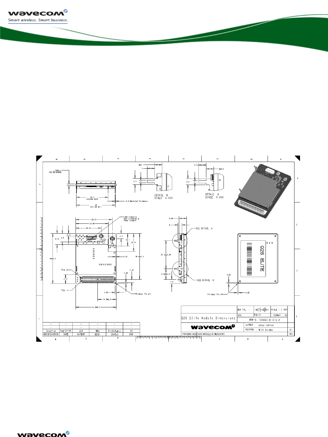
3 Mechanical
The Q26 Elite Wireless CPU® is a member of the Q26 Family. It therefore has
common length and width dimensions as the other Q26 Wireless CPU®s. The
system connector physical attributes are identical as well as its placement.
The primary RF connector and placement are also consistent with the rest of
the family.
3.1 Mechanical Drawing
Figure 1: Mechanical Drawing
© Confidential Page: 13 / 18
This document is the sole and exclusive property of WAVECOM. Not to be distributed or divulged without prior
written agreement.
WI_DEV_Q26EL_UGD_002-002 April 17, 2009
Q26 Elite User Manual
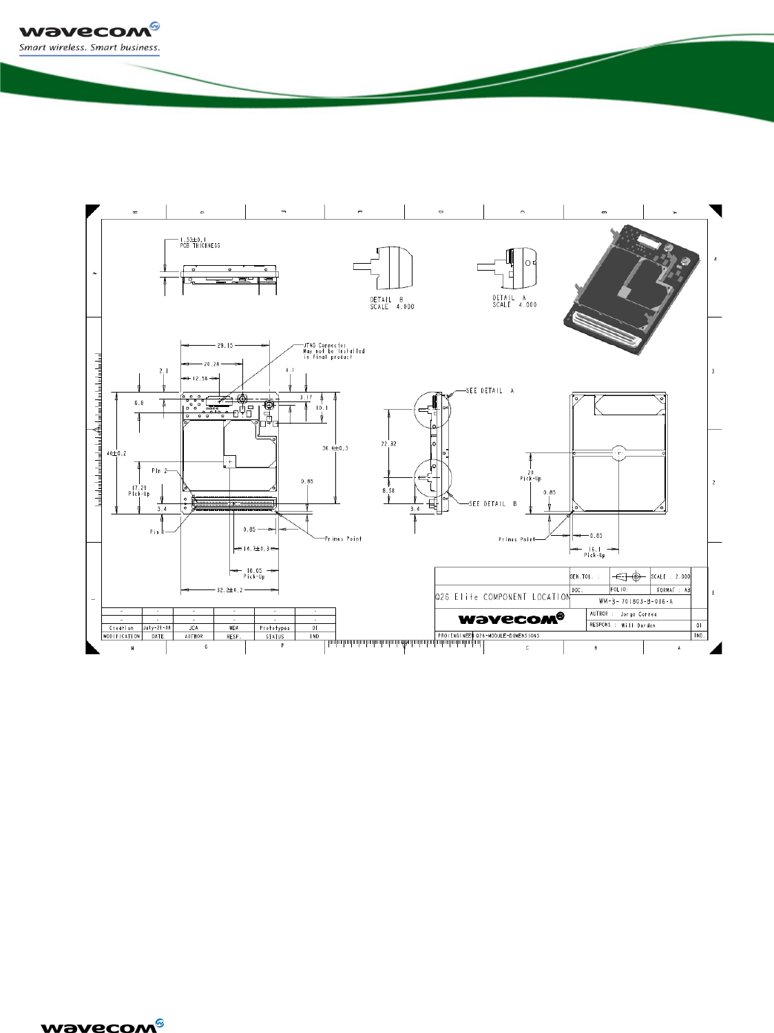
3.2 Component Location Drawing
Figure 2: Component Location Drawing
© Confidential Page: 14 / 18
This document is the sole and exclusive property of WAVECOM. Not to be distributed or divulged without prior
written agreement.
WI_DEV_Q26EL_UGD_002-002 April 17, 2009
Q26 Elite User Manual
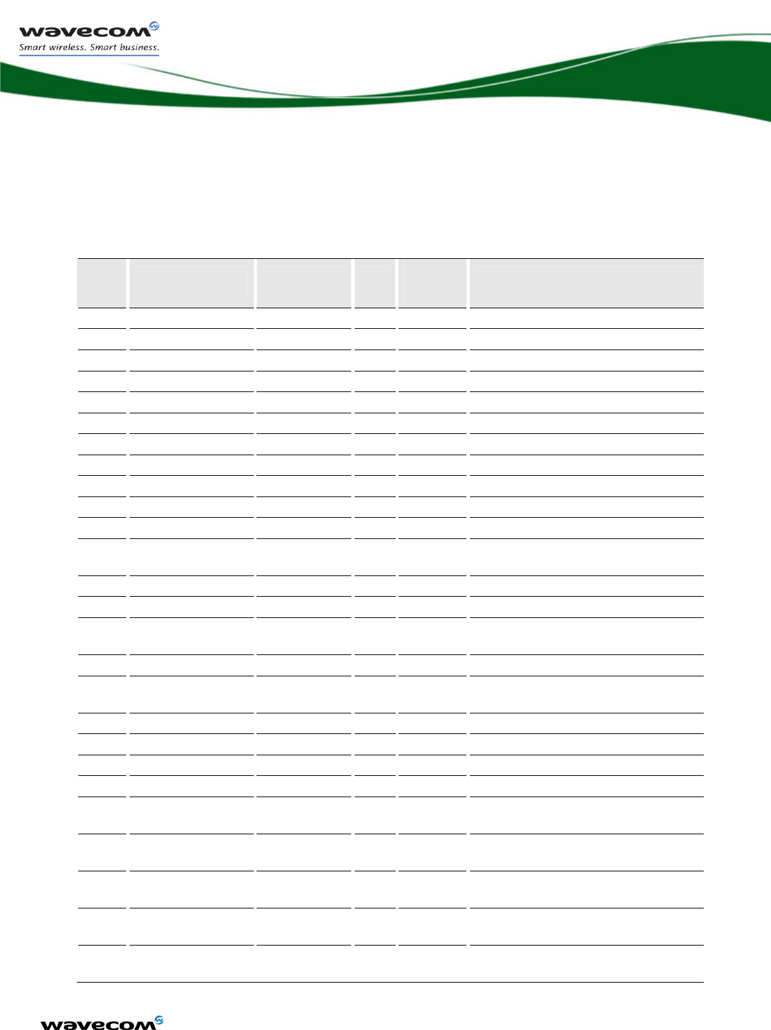
4 System Connector Pin-out
Table 6: System Connector Pin-out
Pin
# Signal Name Voltage I/O*
Pin
Type Description
1 VBATT VBATT I AI Power Supply
2 VBATT VBATT I AI Power Supply
3 VBATT VBATT I AI Power Supply
4 VBATT VBATT I AI Power Supply
5 VCC_1V8 VCC_1V8 O AO 1.8V Supply Output
6 CHG-IN CHG-IN I AI Charger input
7 VCOIN VCOIN I/O AI, AO RTC Battery connection
8 CHG-IN CHG-IN I AI Charger input
9 UIM_PWR 1V8 or 3V O AO UIM Power Supply
10 VCC_2V8 VCC_2V8 O AO 2.8V Supply Output
11 UIM_DATA 1V8 or 3V I/O B6 UIM Data
12 GPIO2 VCC_1V8* I/O
BS-
PD2
13 UIM_RESET 1V8 or 3V O DO2 UIM reset Output
14 UIM_CLK 1V8 or 3V O DO2 UIM Clock
15 VIB_DRV_N Open
Drain O Buzzer Output
16 BOOT VCC_1V8* I Not Used
17 LED Open
Drain O Flash Led Output
18 RESET_N VCC_1V8 I/O RESET Input
19 ON/~OFF VBATT I ON / ~OFF Control
20 ADC_0 Analog I AI Analog to Digital Input
21 ADC_1 Analog I AI Analog to Digital Input
22 GPIO32 VCC_2V8 I/O
BS-
PD2
23 GPIO33 VCC_2V8 I/O
BS-
PD2
24 GPIO34 VCC_2V8 I/O
BS-
PD2
25 GPIO35 VCC_2V8 I/O
BS-
PD2
26 GPIO36 VCC_2V8 I/O
BS-
PD2
© Confidential Page: 15 / 18
This document is the sole and exclusive property of WAVECOM. Not to be distributed or divulged without prior
written agreement.
WI_DEV_Q26EL_UGD_002-002 April 17, 2009
Q26 Elite User Manual
Pin
# Signal Name Voltage I/O*
Pin
Type Description
27 GPIO37 VCC_2V8 I/O
BS-
PD2
28 GPIO38 VCC_2V8 I/O
BS-
PD2
29 GPIO39 VCC_2V8 I/O
BS-
PD2
30 RXD2 VCC_1V8 O DO6 Auxiliary RS232 Receive
31 TXD2 VCC_1V8 I DI Auxiliary RS232 Transmit
32 CTS2 VCC_1V8 O DO2 Auxiliary RS232 Clear To
Send
33 RTS2 VCC_1V8 I DI Auxiliary RS232 Request To
Send
34 MIC2N Analog I AI Micro 2 Input Negative
35 HPH_OUT_L_P Analog O AO Speaker 1 Output Positive,
32 Ohm Output
36 MIC2P Analog I AI Micro 2 Input Positive
37 HPH_OUT_R_N Analog O AO Speaker 1 Output Negative,
32 Ohm Output
38 LINE_IN_R_N Analog I AI Micro 1 Input Negative
39 SPKR_OUT_P Analog O AO Speaker 2 Output Positive, 8
Ohm Output
40 LINE_IN_L_P Analog I AI Micro 1 Input Positive
41 SPKR_OUT_N Analog O AO Speaker 2 Output Negative,
8 Ohm Output
42 EBI2_LB_N VCC_1V8 O DO10 Lower Byte select
43 GPIO40 VCC_2V8 I/O
BS-
PD2
44 SCL VCC_2V8 O B2 I²C Clock
45 GPIO41 VCC_2V8 I/O
BS-
PD2
46 SDA VCC_2V8 I/O B2 I²C Data
47 GPIO42 VCC_2V8 I/O
BS-
PD2
48 GPIO43 VCC_2V8 I/O
BS-
PD2
49 GPIO44 VCC_2V8 I/O
BS-
PD2
50 GPIO7 VCC_1V8* I/O
51 GPIO51 VCC_1V8 I/O
BS-
NP6
52 VPAD-USB VPAD-
USB I AI USB Power supply input

© Confidential Page: 16 / 18
This document is the sole and exclusive property of WAVECOM. Not to be distributed or divulged without prior
written agreement.
WI_DEV_Q26EL_UGD_002-002 April 17, 2009
Q26 Elite User Manual
Pin
# Signal Name Voltage I/O*
Pin
Type Description
53 GPIO50 VCC_1V8* I/O
BS-
PD2
54 USB-DP VPAD-
USB I/O AI, AO USB Data
55 GPIO45 VCC_2V8 I/O
BS-
PD2
56 USB-DM VPAD-
USB I/O AI, AO USB Data
57 GPIO46 VCC_2V8 I/O
BS-
PD2
58 GPIO49 VCC_2V8 I/O
BS-
PU2
59 COL0 VCC_1V8* I/O BS2 Keypad column 0
60 COL1 VCC_1V8* I/O BS2 Keypad column 1
61 COL2 VCC_1V8* I/O BS2 Keypad column 2
62 COL3 VCC_1V8* I/O BS2 Keypad column 3
63 COL4 VCC_1V8* I/O BS2 Keypad column 4
64 ROW4 VCC_1V8* I/O DO2 Keypad Row 4
65 ROW3 VCC_1V8* I/O DO2 Keypad Row 3
66 ROW2 VCC_1V8* I/O DO2 Keypad Row 2
67 ROW1 VCC_1V8* I/O DO2 Keypad Row 1
68 ROW0 VCC_1V8* I/O DO2 Keypad Row 0
69 RI1 VCC_2V8 O BS-
PD2 Main RS232 Ring Indicator
70 DCD1 VCC_2V8 O BS-
PD2
Main RS232 Data Carrier
Detect
71 TXD1 VCC_2V8 I DI Main RS232 Transmit
72 RTS1 VCC_2V8 I DI Main RS232 Request To
Send
73 RXD1 VCC_2V8 O DO4 Main RS232 Receive
74 DSR1 VCC_2V8 O BS-
PD2 Main RS232 Data Set Ready
75 CTS1 VCC_2V8 O DO4 Main RS232 Clear To Send
76 DTR1 VCC_2V8 I BS-
PD2
Main RS232 Data Terminal
Ready
77 PCM_SYNC VCC_1V8* O B2 PCM Frame Synchro
78 PCM_DIN VCC_1V8* I B2 PCM Data Input
79 PCM_CLK VCC_1V8* O B2 PCM Clock
80 PCM_DOUT VCC_1V8* O B2 PCM Data Output
81 EBI2_OE_N VCC_1V8 O DO10
Output Enable/ Read not
write
© Confidential Page: 17 / 18
This document is the sole and exclusive property of WAVECOM. Not to be distributed or divulged without prior
written agreement.
WI_DEV_Q26EL_UGD_002-002 April 17, 2009
Q26 Elite User Manual
Pin
# Signal Name Voltage I/O*
Pin
Type Description
82 Reserved VPAD-
USB Reserved
83 EBI2_CS0_N VCC_1V8 O DO10 Chip Select
84 EBI2_WE_N VCC_1V8 O DO10 Write Enable
85 EBI2_AD0 VCC_1V8 I/O B-K10 Data for Peripheral
86 EBI2_AD15 VCC_1V8 I/O B-K10 Data for Peripheral
87 EBI2_AD1 VCC_1V8 I/O B-K10 Data for Peripheral
88 EBI2_AD14 VCC_1V8 I/O B-K10 Data for Peripheral
89 EBI2_AD2 VCC_1V8 I/O B-K10 Data for Peripheral
90 EBI2_AD13 VCC_1V8 I/O B-K10 Data for Peripheral
91 EBI2_AD3 VCC_1V8 I/O B-K10 Data for Peripheral
92 EBI2_AD12 VCC_1V8 I/O B-K10 Data for Peripheral
93 EBI2_AD4 VCC_1V8 I/O B-K10 Data for Peripheral
94 EBI2_AD11 VCC_1V8 I/O B-K10 Data for Peripheral
95 EBI2_AD5 VCC_1V8 I/O B-K10 Data for Peripheral
96 EBI2_AD10 VCC_1V8 I/O B-K10 Data for Peripheral
97 EBI2_AD6 VCC_1V8 I/O B-K10 Data for Peripheral
98 EBI2_AD9 VCC_1V8 I/O B-K10 Data for Peripheral
99 EBI2_AD7 VCC_1V8 I/O B-K10 Data for Peripheral
100 EBI2_AD8 VCC_1V8 I/O B-K10 Data for Peripheral
*NOTE: I = Inputs to the Q26 Elite and O = Outputs from the Q26 Elite.
Table 7: Pin Type Definition
Symbol Description
Pad type
AI Analog input
AO Analog output
B, BS Bidirectional, bidirectional with Schmitt trigger
DI, DIS Digital CMOS input, digital input with Schmitt trigger
DO Digital output
Pad type - pull/keep details for digital I/Os
PU Contains an internal pullup device
PD Contains an internal pulludown device
K Contains an internal weak keeper device (keepers cannot drive
external buses)
# Drive Strength for digital I/Os

© Confidential Page: 18 / 18
This document is the sole and exclusive property of WAVECOM. Not to be distributed or divulged without prior
written agreement.
WI_DEV_Q26EL_UGD_002-002 April 17, 2009
Q26 Elite User Manual
5 FCC Certification
The Q26 Elite is FCC certified as a ‘mobile device’, which requires a minimum
distance of 20 cm between the application’s antenna and the human body.
Per FCC Section 15.21, any changes or modifications to the Q26 Elite not
expressly approved by Wavecom could void the user's authority to operate the
equipment.
Users and installers must be provided with antenna installation instructions
and transmitter operating conditions for satisfying RF exposure compliance.
Wavecom’s FCC ID may be used by the integrator if the conditions below are
followed:
1. The application must be implemented as a “mobile device” and not a
“portable device.”
2. The application’s user and installation manuals must include a
statement that a minimum distance of 20 cm between the antenna and
the human body is required.
3. The antenna system gain must be within the following constraints:
a) 850 MHz Band: the antenna system gain must not exceed 5.76
dBd gain.
b) 1900 MHz PCS Band: the antenna system gain must not
exceed 7.01 dBi gain.
4. The license module will have a FCC ID label on the module itself. The
FCC ID label must be visible as defined by the FCC (visible through an
open access door is permissible), or a separate label must be similarly
visible that conveys the message: “Contains Transceiver Module FCC ID:
O9EQ26ELITE.”

WAVECOM S.A. : 3 esplanade du Foncet - 92442 Iss
y
-les-Moulineaux - France - Tel: +33 1 46 29 08 00 - Fax: +33 1 46 29 08 08
Wavecom, Inc: 430 Davis Drive, Suite 300 Research Triangle Park, North Carolina, USA - Tel: +1 919 237 4000 - Fax: +1 919 237 4140
WAVECOM Asia-Pacific: Unit 201-207, 2nd Floor, Bio-Informatics Centre No. 2 Science Park West Avenue, Hong Kong Science Park,
Shatin, New Territories, Hong Kong (PRC) - Tel: +852-2824 0254 - Fax: +852-2824 0255 [Online contact details, GPS and maps]