Sierra Wireless Q26EX Q26 Extreme wireless CPU User Manual
Sierra Wireless, Inc. Q26 Extreme wireless CPU
User Manual
WM_DEV_Q26EX_PTS_002
006
December 3, 2009
Q26 Extreme Wireless CPU®
Product Technical Specification
and Customer Design Guidelines

WM_DEV_Q26EX_PTS_002 Rev 006 Page 2 of 112
Product Technical Specification and
Customer Design Guidelines
Due to the nature of wireless communications, transmission and reception of data can never be
guaranteed. Data may be delayed, corrupted (i.e., have errors) or be totally lost. Although significant
delays or losses of data are rare when wireless devices such as the Sierra Wireless modem are used in
a normal manner with a well-constructed network, the Sierra Wireless modem should not be used in
situations where failure to transmit or receive data could result in damage of any kind to the user or
any other party, including but not limited to personal injury, death, or loss of property. Sierra
Wireless accepts no responsibility for damages of any kind resulting from delays or errors in data
transmitted or received using the Sierra Wireless modem, or for failure of the Sierra Wireless modem
to transmit or receive such data.
Do not operate the Sierra Wireless modem in areas where blasting is in progress, where explosive
atmospheres may be present, near medical equipment, near life support equipment, or any
equipment which may be susceptible to any form of radio interference. In such areas, the Sierra
Wireless modem MUST BE POWERED OFF. The Sierra Wireless modem can transmit signals that
could interfere with this equipment. Do not operate the Sierra Wireless modem in any aircraft,
whether the aircraft is on the ground or in flight. In aircraft, the Sierra Wireless modem MUST BE
POWERED OFF. When operating, the Sierra Wireless modem can transmit signals that could
interfere with various onboard systems.
Note: Some airlines may permit the use of cellular phones while the aircraft is on the ground and the door is
open. Sierra Wireless modems may be used at this time.
The driver or operator of any vehicle should not operate the Sierra Wireless modem while in control
of a vehicle. Doing so will detract from the driver or operator’s control and operation of that vehicle.
In some states and provinces, operating such communications devices while in control of a vehicle is
an offence.

WM_DEV_Q26EX_PTS_002 Rev 006 Page 3 of 112
Product Technical Specification and
Customer Design Guidelines
This manual is provided “as is”. Sierra Wireless makes no warranties of any kind, either expressed or
implied, including any implied warranties of merchantability, fitness for a particular purpose, or
noninfringement. The recipient of the manual shall endorse all risks arising from its use.
The information in this manual is subject to change without notice and does not represent a
commitment on the part of Sierra Wireless. SIERRA WIRELESS AND ITS AFFILIATES
SPECIFICALLY DISCLAIM LIABILITY FOR ANY AND ALL DIRECT, INDIRECT, SPECIAL,
GENERAL, INCIDENTAL, CONSEQUENTIAL, PUNITIVE OR EXEMPLARY DAMAGES
INCLUDING, BUT NOT LIMITED TO, LOSS OF PROFITS OR REVENUE OR ANTICIPATED
PROFITS OR REVENUE ARISING OUT OF THE USE OR INABILITY TO USE ANY SIERRA
WIRELESS PRODUCT, EVEN IF SIERRA WIRELESS AND/OR ITS AFFILIATES HAS BEEN
ADVISED OF THE POSSIBILITY OF SUCH DAMAGES OR THEY ARE FORESEEABLE OR FOR
CLAIMS BY ANY THIRD PARTY.
Notwithstanding the foregoing, in no event shall Sierra Wireless and/or its affiliates aggregate
liability arising under or in connection with the Sierra Wireless product, regardless of the number of
events, occurrences, or claims giving rise to liability, be in excess of the price paid by the purchaser
for the Sierra Wireless product.
© 2009 Sierra Wireless. All rights reserved.
AirCard® and “Heart of the Wireless Machine®” are filed or registered trademarks of Sierra Wireless.
Watcher® is a trademark of Sierra Wireless, registered in the European Community. Sierra Wireless,
the Sierra Wireless logo, the red wave design, and the red-tipped antenna are trademarks of Sierra
Wireless.
, , ®, inSIM®, “YOU MAKE IT, WE MAKE IT WIRELESS®”,
WAVECOM®, WISMO®, Wireless Microprocessor®, Wireless CPU®, Open AT® are filed or registered
trademarks of Sierra Wireless S.A. in France and/or in other countries.
Windows® is a registered trademark of Microsoft Corporation.
QUALCOMM® is a registered trademark of QUALCOMM Incorporated. Used under license.
Other trademarks are the property of the respective owners.

WM_DEV_Q26EX_PTS_002 Rev 006 Page 4 of 112
Product Technical Specification and
Customer Design Guidelines
Sales Desk:
Phone:
1-604-232-1488
Hours:
8:00 AM to 5:00 PM Pacific Time
E-mail:
Post:
Sierra Wireless
13811 Wireless Way
Richmond, BC
Canada V6V 3A4
Fax:
1-604-231-1109
Web:
Consult our website for up-to-date product descriptions, documentation, application notes, firmware
upgrades, troubleshooting tips, and press releases:
Level
Date
List of revisions
001
December 22, 2008
Creation
002
March 18, 2009
Update power consumption figures add thermal design rules
003
June 05, 2009
Update for Vbatt range, thermal foam and temperature behavior
004
August 4, 2009
Reformatted in Sierra Wireless style.
Updated UART1 tolerance information as follows: The UART1 interface is
a 2.8 volts type. Moreover, it is 3.3 volts tolerant.
Updated Standards and Recommendations section.
005
September 16, 2009
Updated Antenna gain of 4.6dBi and additional information in this
paragraph of the Standards Recommendations section.
Updated CT104-RXD1* to be MUXed with GPIO37
006
December 3, 2009
Standards and Recommendations section:
Updated FCC notice by adding to the last sentence of one paragraph
regarding FCC multi-transmitter information, deleted the following
one sentence regarding compliance, and fixed the values in the
following sentence to 4.6dBi (850MHz) and 3.4dBi (1900MHz) .
Interfaces section:
Updated 3V/1V8 UICC/SIM interface bullet
Updated USIM/SIM card bullet
USIM/SIM Interface section
Added Using the USIM is recommended over the SIM card sentence
WM_DEV_Q26EX_PTS_002 Rev 006 Page 13 of 112
Product Technical Specification and
Customer Design Guidelines
This document presents and defines the Q26 Extreme Wireless CPU®.
The Q26 Extreme Wireless CPU® is a multi-mode EDGE 2G / WCDMA 3G / HSxPA (High Speed
Downlink & High Speed Uplink Packet Access) solution with dual antenna receive diversity,
footprint compatible with other Wireless CPU® Q26 devices.
The Q26 Extreme Wireless CPU® supports a powerful open software platform (Open AT®). Open AT®
is the world’s most comprehensive cellular development environment, which allows embedded
standard ANSI C applications to be natively executed directly on the Wireless CPU®.
This Product Specification document covers the Wireless CPU® alone and does not include the
programmable capabilities provided via the use of Open AT® Software Suites.
For more details, several reference documents may be consulted. The Wavecom reference documents
are provided in the Wavecom document package, contrary to the general reference documents which
are not authored by Wavecom.
Please check the web site for the latest documentation available.
First Software version available for Q26 Extreme Wireless CPU® is Open AT® Software Suite v2.30.
[1] Getting Started with Open AT®
[2] Basic Development Guide for Open AT®
[3] ADL User Guide for Open AT®
[4] Open AT® Release Note
[5] Open AT® Firmware v7.4 AT Commands Manual (Ref: WM_DEV_OAT_UGD_079-010)
[6] Open AT® Firmware Release Note

WM_DEV_Q26EX_PTS_002 Rev 006 Page 14 of 112
Product Technical Specification and
Customer Design Guidelines
[7] “I²C Bus Specification and user guide”, Version 3.0, NXP 2007
[8] ISO 7816-3 Standard
Table 1. Abbreviations
Abbreviation
Definition
AC
Alternating Current
ADC
Analog to Digital Converter
A/D
Analog to Digital conversion
AF
Audio-Frequency
AT
ATtention (prefix for modem commands)
AUX
AUXiliary
CAN
Controller Area Network
CB
Cell Broadcast
CEP
Circular Error Probable
CLK
CLocK
CMOS
Complementary Metal Oxide Semiconductor
CS
Coding Scheme
CTS
Clear To Send
DAC
Digital to Analog Converter
dB
Decibel
DC
Direct Current
DCD
Data Carrier Detect
DCE
Data Communication Equipment
DCS
Digital Cellular System
DR
Dynamic Range
DSR
Data Set Ready
DTE
Data Terminal Equipment
DTR
Data Terminal Ready
EDGE
Enhanced Data rates for GSM Evolution
EFR
Enhanced Full Rate
EGPRS
Enhanced General Packet Radio Service
E-GSM
Extended GSM
EMC
ElectroMagnetic Compatibility
EMI
ElectroMagnetic Interference
EMS
Enhanced Message Service
EN
ENable
ESD
ElectroStatic Discharges
FIFO
First In First Out
WM_DEV_Q26EX_PTS_002 Rev 006 Page 15 of 112
Product Technical Specification and
Customer Design Guidelines
Abbreviation
Definition
FR
Full Rate
FTA
Full Type Approval
GND
GrouND
GPI
General Purpose Input
GPC
General Purpose Connector
GPIO
General Purpose Input Output
GPO
General Purpose Output
GPRS
General Packet Radio Service
GPS
Global Positioning System
GSM
Global System for Mobile communications
HR
Half Rate
HSDPA
High Speed Downlink Packet Access
HSUPA
High Speed Uplink Packet Access
HSxPA
High Speed x(downlink/uplink) Packet Access
I/O
Input / Output
LED
Light Emitting Diode
LNA
Low Noise Amplifier
MAX
MAXimum
MIC
MICrophone
MIN
MINimum
MMS
Multimedia Message Service
MO
Mobile Originated
MT
Mobile Terminated
na
Not Applicable
NF
Noise Factor
NMEA
National Marine Electronics Association
NOM
NOMinal
NTC
Negative Temperature Coefficient
PA
Power Amplifier
Pa
Pascal (for speaker sound pressure measurements)
PBCCH
Packet Broadcast Control CHannel
PC
Personal Computer
PCB
Printed Circuit Board
PCM
Pulse Code Modulation (audio) or Protection Circuit Module (battery)
PDA
Personal Digital Assistant
PFM
Power Frequency Modulation
PSM
Phase Shift Modulation
PWM
Pulse Width Modulation
RAM
Random Access Memory
RF
Radio Frequency
RFI
Radio Frequency Interference
WM_DEV_Q26EX_PTS_002 Rev 006 Page 16 of 112
Product Technical Specification and
Customer Design Guidelines
Abbreviation
Definition
RHCP
Right Hand Circular Polarization
RI
Ring Indicator
RST
ReSeT
RTC
Real Time Clock
RTCM
Radio Technical Commission for Maritime services
RTS
Request To Send
RX
Receive
SCL
Serial CLock
SDA
Serial DAta
SMS
Short Message Service
SPI
Serial Peripheral Interface
SPL
Sound Pressure Level
SPK
SPeaKer
SRAM
Static Random Access Memory
TBC
To Be Confirmed
TDMA
Time Division Multiple Access
TP
Test Point
TVS
Transient Voltage Suppressor
TX
Transmit
TYP
TYPical
UART
Universal Asynchronous Receiver-Transmitter
UMTS
Universal Mobile Telecommunications System
USB
Universal Serial Bus
USIM
Universal Subscriber Identification Module
USSD
Unstructured Supplementary Services Data
VSWR
Voltage Standing Wave Ratio
WCDMA
Wideband Code Division Multiple Access
Table 2. Web Site Support Links
Subject matter
Web site
General information about Wavecom and its range of products:
Specific support about the Q26 Extreme Wireless CPU®:
Carrier/Operator approvals:
Open AT® Introduction:
Developer support for software and hardware:
WM_DEV_Q26EX_PTS_002 Rev 006 Page 17 of 112
Product Technical Specification and
Customer Design Guidelines
The Q26 Extreme Wireless CPU® series is a self-contained GSM/GPRS/EGDE quad-band and HSxPA
tri band Wireless CPU® with the following characteristics:
Dimension:
Length: 40 mm
Width: 32.2 mm
Thickness: 6.3 mm
X/Y form-factor compatible with Q2686/87 Wireless CPU® range
EU Directive 2002/95/EC on RoHS
The Q26 Extreme Wireless CPU® is compliant with RoHS (Restriction of Hazardous
Substances in Electrical and Electronic Equipment) Directive 2002/95/EC which sets limits
for the use of certain restricted hazardous substances.
This directive states that “from 1st July 2006, new electrical and electronic equipment put
on the market does not contain lead, mercury, cadmium, hexavalent chromium,
polybrominated biphenyls (PBB), and polybrominated diphenyl ethers (PBDE)”.
Regulatory: R&TTE directive (CE marking), GCF-CC, PTCRB, FCC/IC.
Manufacturing: ISO/TS 16949
3GPP FDD Release 6 HSUPA Compliant.
Tri-Band UMTS/HxDPA (WCDMA/FDD) 2100/1900/850 MHz (band I, II, V)
Downlink data rates up to HSDPA Category 8 (7.2 Mbps).
Uplink data rates up to HSUPA Category 5 (2 Mbps)
Advanced Type III receiver technology supporting simultaneous Receive Diversity and
Equalization.
Quad-Band GSM GPRS EDGE 850/900/1800/1900 MHz
GPRS class 12
EDGE (E-GPRS) multi-slot class 12
Dual mode with fully automated handover between 2G and 3G networks
Voice: HR, FR and EFR; Adaptive multi-rate AMR in GSM & UMTS.
WM_DEV_Q26EX_PTS_002 Rev 006 Page 18 of 112
Product Technical Specification and
Customer Design Guidelines
Digital section running under 2.8 volts and 1.8 volts.
3V/1V8 UICC/SIM interface
Complete interfacing:
Power supply
Serial link
Analog audio
Parallel bus 16bits
PCM digital audio
USIM/SIM card
Keyboard
USB 2.0 slave FS
Serial LCD (not available with AT commands)
Application processor embeds Open AT® Software Suite with extensive set of Plug-Ins, supported by
M2M Studio, enabling the creation of natively executed code in C and/or Lua script.
Up to 88 MIPS for application execution
Includes a low latency, multitasking pre-emptive Operating System
The Q26 Extreme Wireless CPU® has following external connections:
Two solutions for main RF antenna connection
UFL connector
Soldered connection
Diversity RF antenna connection:
Soldered connection
Analogue and digital interfaces:
100 pin I/O connector.
WM_DEV_Q26EX_PTS_002 Rev 006 Page 19 of 112
Product Technical Specification and
Customer Design Guidelines
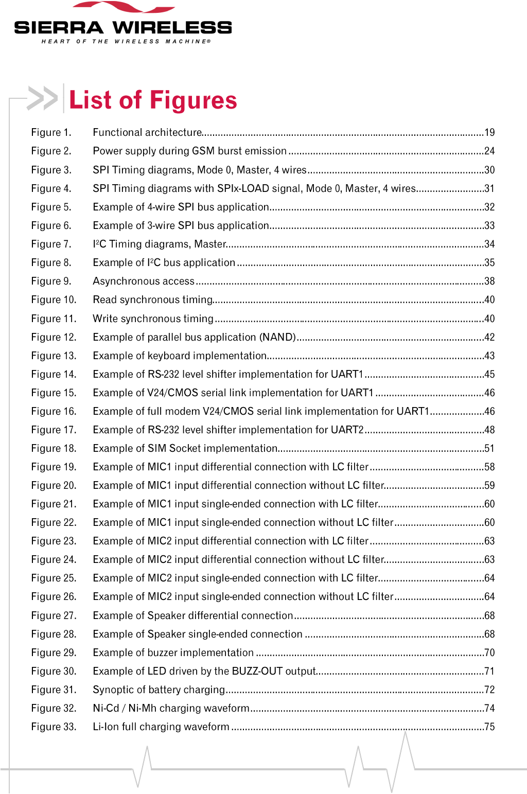
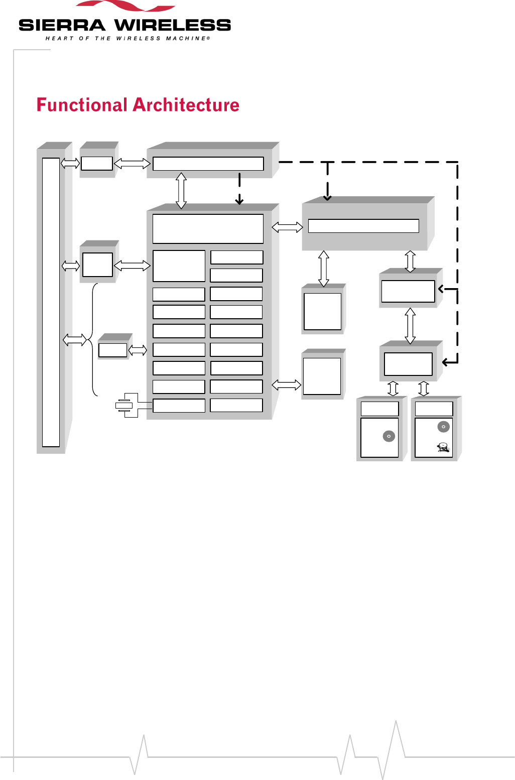
The global architecture of the Q26 Extreme Wireless CPU® is described below:
AUDIO
POWER
UART2
PCM
UART1
USB
SIM 1.8V/3V
EBI
DAC
ADC
GPIO
SPI1
I2C
SPI2
EXT_IT
POWER MANAGEMENT
AUDIO
FILTER
MEMORY
FLASH /
SRAM
RF
FRONT END
2G / 3G RF
TRANSCEIVER
COAX
UFL
MAIN
ANTENNA
Q
2
6
E
X
B
O
A
R
D
T
O
B
O
A
R
D
I
N
T
E
R
F
A
C
E
C
O
N
N
E
C
T
O
R
CHARGER
RTC
USB
detection
KEYPAD
DUAL 2G&3G base band processor
COAX
DIVERSITY
ANTENNA
MEMORY
FLASH /
SDRAM
APPLICATION Processor Core
Figure 1. Functional architecture
WM_DEV_Q26EX_PTS_002 Rev 006 Page 20 of 112
Product Technical Specification and
Customer Design Guidelines
The Radio Frequency (RF) range complies with the Phase II EGSM 900/DCS 1800 and GSM 850/PCS
1900 recommendations. The frequencies are:
Table 3. RF Frequency Ranges
RF Bandwidth
Transmit band (Tx)
Receive band (Rx)
GSM 850
824 to 849 MHz
869 to 894 MHz
E-GSM 900
880 to 915 MHz
925 to 960 MHz
DCS 1800
1710 to 1785 MHz
1805 to 1880 MHz
PSC 1900
1850 to 1910 MHz
1930 to 1990 MHz
WCDMA Band I
1920 to 1980 MHz
2110 to 2170 MHz
WCDMA Band II
1850 to 1910 MHz
1930 to 1990 MHz
WCDMA Band V
824 to 849 MHz
869 to 894 MHz
The Radio Frequency (RF) part is based on a specific quad-band chip with a:
Direct down conversion Rx architecture
Linear direct up-conversion Tx architecture
On chip Tx power control
Analog I/Q base band interface for all modes
Integrated Σ-Δ fractional N synthesiser for dual-mode operation
On chip multi-band true Rx diversity
The Q26 Extreme supports the complete family of software Plug-Ins provided within the Open AT®
Software Suite (TCP-IP, Internet, GPS, Lua, Security, Bluetooth, aqLink™). It also supports
VariPower & VariSpeed (26-104MHz) features allowing highly configurable power optimization:
ARM946 32 bit processor
Programmable to 104MHz operation
Internal Memory (8kbyte Cache I$, 8kbyte D$)
Latency time: < 1ms
Memory access speed up to 52MHz
2 user Timers at 13MHz fine tuning (1 for customer)
3 External IT with debouncing
WM_DEV_Q26EX_PTS_002 Rev 006 Page 21 of 112
Product Technical Specification and
Customer Design Guidelines
The Q26 Extreme Wireless CPU® is designed to integrate various types of specific process applications
such as vertical applications (telemetry, multimedia, automotive).
The Operating System offers a set of AT commands to control the Wireless CPU®. With this standard
Operating System, some interfaces of the Wireless CPU® are not available, since they are dependent
on the peripheral devices connected to the Wireless CPU®.
The Operating System is Open AT® compliant.
WM_DEV_Q26EX_PTS_002 Rev 006 Page 22 of 112
Product Technical Specification and
Customer Design Guidelines
A 100-pin connector is provided to interface the Q26 Extreme Wireless CPU® with a board containing
a serial LCD Wireless CPU®, a keyboard, a USIM connector, or a battery connection.
The available interfaces on the GPC are described below.
Table 4. Available GPC Interfaces
Name
Driven by
AT commands
Driven by
Open AT®
Serial Interface
X
Keyboard Interface
X
X
Main Serial Link
X
X
Auxiliary Serial Link
X
X
USIM Interface
X
X
General Purpose IO
X
X
Analog to Digital Converter
X
X
Analog Audio Interface
X
X
Buzzer Output
X
X
Battery Charging Interface
X
X
External Interruption
X
X
VCC_2V8 and VCC_1V8
BAT-RTC (Backup Battery)
LED0 signal
X
X
Digital Audio Interface (PCM)
X
USB 2.0 Interface
X
X
WM_DEV_Q26EX_PTS_002 Rev 006 Page 23 of 112
Product Technical Specification and
Customer Design Guidelines
Only the VBATT input is necessary to supply the Q26 Extreme Wireless CPU®.
Operational average current
Recommended values for Operational average max current: 1.1A
Peak max current
Recommended values for Peak max current: 2.1A.
The rising time is around 10µs
See subsection g) for worst case description.
Ground
The Q26 Extreme Wireless CPU® shielding case is the grounding. The ground must be connected to
the motherboard through a complete layer on the PCB.
Table 5. Input power supply voltage
Vmin
Vnom
Vmax
VBATT1,2
3.4V
3.8V
4.2V
(1): This value must be guarantied during the burst (with 2.1A Peak in GSM or GPRS mode)
(2): Max operating Voltage Stationary Wave Ratio (VSWR) 2:1
Impedance
When the Wireless CPU® is supplied with a battery, the total impedance (battery + protections + PCB)
should be < 150 mΩ.
Recommendations when using DC/DC converter
As the radio power amplifier is directly connected to VBATT, the Wireless CPU® is sensitive to any
Alternative Current on lines. When a DC/DC converter is used, Wavecom recommends setting the
converter frequency in such a way that the resulting voltage does not exceed the values in following
table.
Table 6. Maximum voltage ripple (Uripp) vs. Frequency
Freq. (Hz)
Uripp Max (mVpp)
f 300
80
300 < f 800
10
800 < f 1100
30
WM_DEV_Q26EX_PTS_002 Rev 006 Page 24 of 112
Product Technical Specification and
Customer Design Guidelines
Freq. (Hz)
Uripp Max (mVpp)
f > 1100
60
Constraints in Alarm/Off mode
When the Wireless CPU® is in Alarm/Off mode, no voltage has to be applied on any pin of the 100-pin
connector, except on Vbatt (pins 1 to 4), BAT-RTC (pin 7) for RTC operation or ON/~OFF (pin 19) to
power-ON the Wireless CPU®.
Details
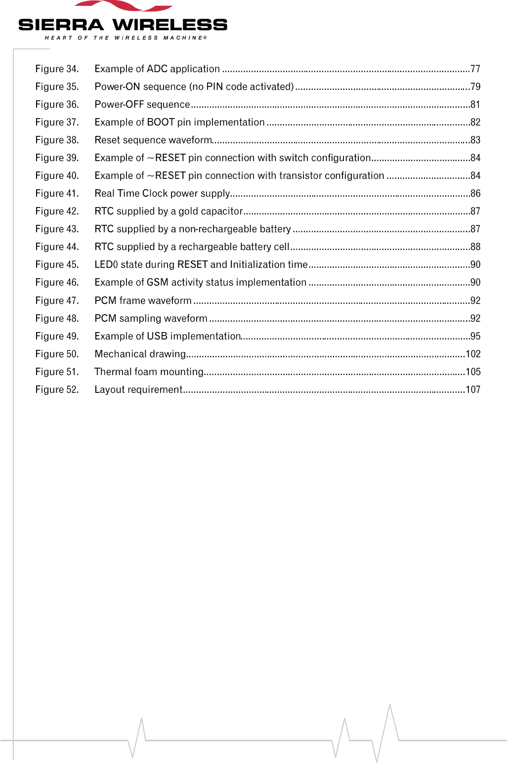
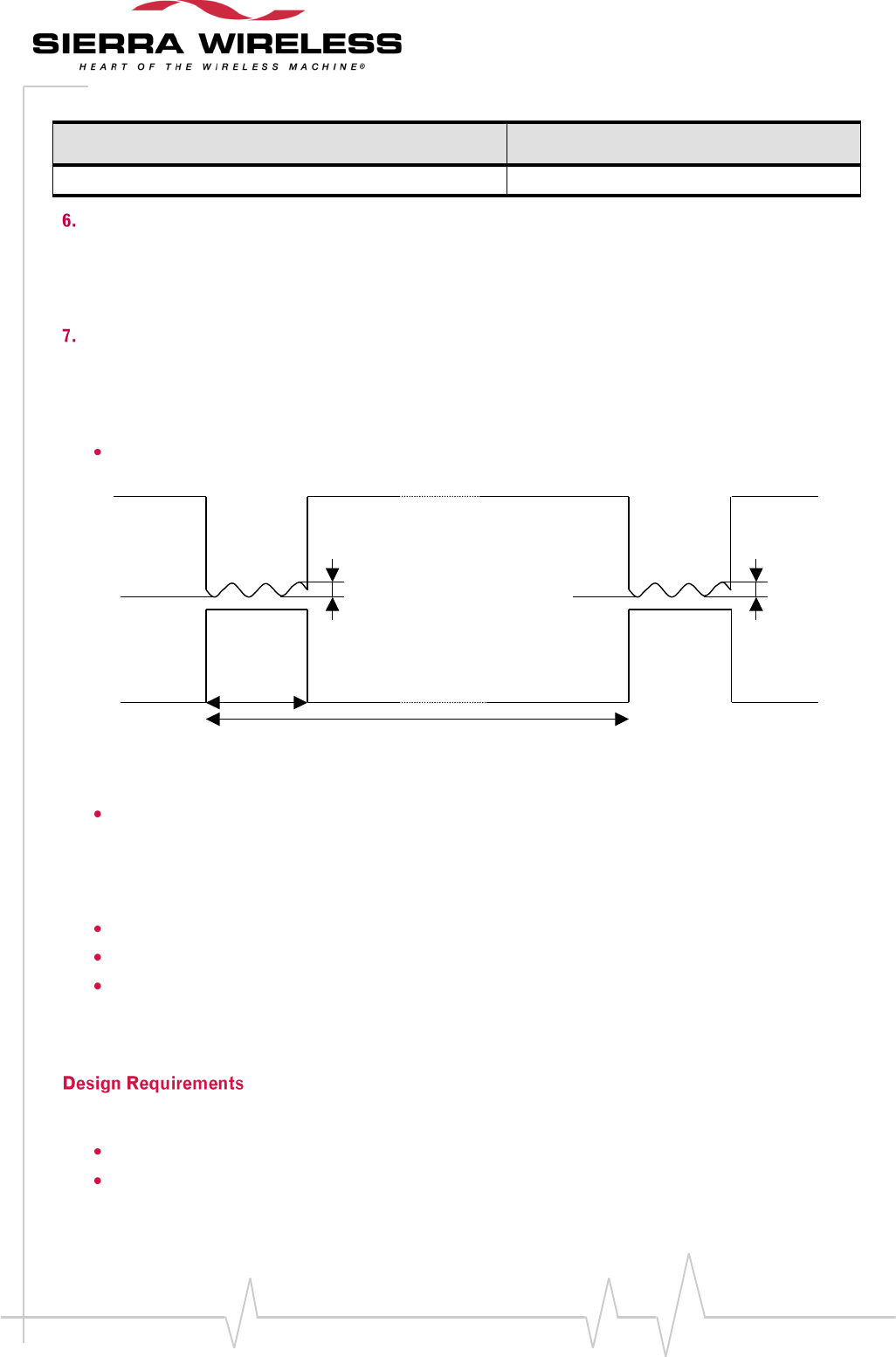
Due to the burst emission mode used in GSM/GPRS/EGPRS, the power supply must be able to deliver
high current peaks in a short time. During the peaks, the ripple (Uripp) on the supply voltage must not
exceed a certain limit).
In communication mode, a GSM/GPRS class 2 terminal emits 577µs radio bursts every
4.615ms.
Uripp
VBATTT
Uripp
T = 4,615 ms
t = 577 µs
Figure 2. Power supply during GSM burst emission
Directly supplies the RF components with 3.8 V. It is essential to keep a minimum voltage
ripple at this connection in order to avoid any phase error.
The RF Power Amplifier current (2.1A max peak in GSM /GPRS mode) flows with a ratio of:
1/8 of the time (577µs every 4.615ms for GSM /GPRS cl. 2) and
2/8 of the time (1154µs every 4.615ms for GSM /GPRS cl. 10).
4/8 of the time (2302µs every 4.615ms for GSM /GPRS cl. 12).
The rising time is around 10µs.
Attention should be paid:
to the quality of the power supply:
linear regulation (recommended) or PWM (Pulse Width Modulation) converter (usable) are
preferred for low noise.
WM_DEV_Q26EX_PTS_002 Rev 006 Page 25 of 112
Product Technical Specification and
Customer Design Guidelines
PFM (Power Frequency Modulation) or PSM (Phase Shift Modulation) system must be
avoided.
to the capacity to deliver high current peaks in a short time (burst radio emission).
that the VBATT line supports peak currents with an acceptable voltage drop which
guarantees a VBATT minimal value of 3.4V.
For PCB design constraints related to power supply tracks, ground planes and shielding, refer to the
Design Guidelines section.
Decoupling capacitors on VBATT lines are embedded in the Wireless CPU. Hence, it should not be
necessary to add decoupling capacitors close to the Wireless CPU.
However, in case of EMI/RFI problem, VBATT signal may require some EMI/RFI decoupling: parallel
33 pF capacitor close to the Wireless CPU or a serial ferrite bead (or both to get better results). Low
frequency decoupling capacitors (22µF to 100µF) may be used to reduce the TDMA noise (217Hz).
Caution: When ferrite beads are used, the recommendation given for the power supply connection must
be followed with care (as high current capacity and low impedance).
Power consumption is dependent on the configuration used. It is for this reason that the following
consumption values are given for each mode, RF band and type of software used (AT or Open AT®).
All the following information is given assuming a 50 ohms RF output.
The following consumption values were obtained by performing measurements on the Wireless
CPU® samples at a temperature of 25° C.
Three VBATT values are used to measure the consumption, VBATTmin (3.4V), VBATTmax (4.2V) and
VBATTtyp (3.8V).
The average current is given for the three VBATT values and the peak current given is the maximum
current peak measured with the three VBATT voltages.
For a more detailed description of the operating modes, see the appendix of the AT Command User
Guide [5].
First let’s define start-up current in view to avoid start issues.
The following measurement results are relevant when there is no Open AT® application.
For explanation of power consumption mode, please Open AT® feature navigator document available
on Wavecom website.
WM_DEV_Q26EX_PTS_002 Rev 006 Page 26 of 112
Product Technical Specification and
Customer Design Guidelines
Table 7. Power Consumption without Open AT® Processing
Operating Mode
Power Consumption
Parameters
INOM average
Unit
VBATT=3.8V
Min
Typ
Max
ALARM Mode
16
µA
SLEEP Mode
1.4
mA
ACTIVE Mode
24.5
mA
SLEEP mode with
telecom stack in Idle
Mode 1
Case 2G (Paging 9/Rx burst occurrence ~2s)
3.1
mA
Case 2G (Paging 2/Rx burst occurrence ~0,5s)
6.4
mA
Case WCDMA (Paging 9)
2
mA
ACTIVE mode with
telecom stack in Idle
Mode 1
Case 2G (Paging 9/Rx burst occurrence ~2s)
28.6
mA
Case 2G (Paging 2/Rx burst occurrence ~0,5s)
32.8
mA
Case WCDMA (Paging 9)
27.6
mA
Peak current in
GSM/GPRS Mode
850/900 MHz - PCL5/gam.3 (TX power 33dBm)
2.1
A
1800/1900 MHz - PCL0/gam.3 (TX power 30dBm)
1.7
A
GSM Connected Mode
(Voice)
850/900 MHz - PCL5 (TX power 33dBm)
470
mA
850/900 MHz - PCL19 (TX power 5dBm)
300
mA
1800/1900 MHz - PCL0 (TX power 30dBm)
420
mA
1800/1900 MHz - PCL15 (TX power 0dBm)
290
mA
GPRS Transfer Mode
class 8 (4Rx/1Tx)
850/900 MHz - gam. 3(TX power 33dBm)
455
mA
1800/1900 MHz - gam.3(TX power 30dBm)
415
mA
GPRS Transfer Mode
class 10 (3Rx/2Tx)
850/900 MHz - gam.3 (TX power 30dBm)
570
mA
1800/1900 MHz - gam.3 (TX power 27dBm)
500
mA
GPRS Transfer Mode
class 12 (1Rx/4Tx)
850/900 MHz - gam.3 (TX power 27dBm)
720
mA
1800/1900 MHz - gam.3 (TX power 24dBm)
620
mA
EGPRS Transfer Mode
class 8 (4Rx/1Tx)
850/900 MHz - gam.6 (TX power 27dBm)
385
mA
1800/1900 MHz - gam.5 (TX power 26dBm)
380
mA
EGPRS Transfer Mode
class 10 (3Rx/2Tx)
850/900 MHz - gam.6 (TX power 24dBm)
480
mA
1800/1900 MHz - gam.5 (TX power 23dBm)
460
mA
EGPRS Transfer Mode
class 12 (1Rx/4Tx)
850/900 MHz - gam.6 (TX power 21dBm)
640
mA
1800/1900 MHz - gam.5 (TX power 20dBm)
600
mA
UMTS Connected Mode
(Voice)
BAND I @ +22 dBm
780
810
mA
BAND I @ +10 dBm
570
mA
BAND II @ +22 dBm
821
920
mA
BAND II @ +10 dBm
570
mA
BAND V @ +22 dBm
780
825
mA
BAND V @ +10 dBm
535
mA
WM_DEV_Q26EX_PTS_002 Rev 006 Page 27 of 112
Product Technical Specification and
Customer Design Guidelines
Operating Mode
Power Consumption
UMTS Data Transfer2
384kbits/s
BAND I @ +22 dBm
855
885
mA
BAND I @ +10 dBm
645
mA
BAND II @ +22 dBm
860
930
mA
BAND II @ +10 dBm
635
mA
BAND V @ +22 dBm
825
870
mA
BAND V @ +10 dBm
550
mA
HSDPA Data Transfer2
Cat. 8
7.2Mbits/s
BAND I @ +22 dBm
915
945
mA
BAND I @ +10 dBm
720
mA
BAND II @ +22 dBm
935
1050
mA
BAND II @ +10 dBm
720
mA
BAND V @ +22 dBm
875
920
mA
BAND V @ +10 dBm
625
mA
HSUPA Data Transfer2
Cat. 5
2Mbist/s
BAND I @ +22 dBm
890
920
mA
BAND I @ +10 dBm
705
mA
BAND II @ +22 dBm
920
990
mA
BAND II @ +10 dBm
710
mA
BAND V @ +22 dBm
875
920
mA
BAND V @ +10 dBm
625
mA
TX means that the current peak is the RF transmission burst (Tx burst)
RX means that the current peak is the RF reception burst (Rx burst)
1 This Mode consumption is dependent on the USIM card used. Some USIM cards respond faster than others, the longer
the response time, the higher the consumption. The measurements were performed with a large number of 3V USIM
cards, the results in brackets are the minimum and maximum currents measured from among all the USIMs used.
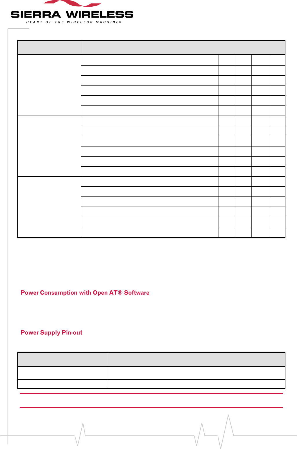
The activation of the Open AT® software could increase the power consumption up to 60mA in
ACTIVE mode and CONNECTED when the full CPU load is used by the Open AT® application.
Table 8. Power supply pin-out
Signal
Pin number
VBATT
1,2,3,4
GND
Shielding
Caution: The grounding connection is made through the shielding
the four leads must be soldered to
the ground plane.
WM_DEV_Q26EX_PTS_002 Rev 006 Page 28 of 112
Product Technical Specification and
Customer Design Guidelines
The three types of digital I/O on the Q26 Extreme Wireless CPU® are: 2.8Volt CMOS, 1.8Volt CMOS
and Open drain.
The three types are described below:
Table 9. 2.8 Volt type (2V8 )
Parameter
I/O type
Minim.
Typ
Maxim.
Condition
Internal 2.8V power supply
VCC_2V8
2.74V
2.8V
2.86V
Input / Output pin
VIL
CMOS
-0.5V*
0.84V
VIH
CMOS
1.96V
3.2V*
VOL
CMOS
0.4V
IOL = - 4 mA
VOH
CMOS
2.4V
IOH = 4 mA
IOH
4mA
IOL
- 4mA
*Absolute maximum ratings
All 2.8V I/O pins do not accept input signal voltage above the maximum voltage specified above,
except for the UART1 interface, which is 3.3V tolerant.
Table 10. 1.8 Volt type (1V8)
Parameter
I/O type
Minim.
Typ
Maxim.
Condition
Internal 1V8 power supply
VCC_1V8
1.76V
1.8V
1.94V
Input / Output pin
VIL
CMOS
-0.5V*
0.54V
VIH
CMOS
1.33V
2.2V*
VOL
CMOS
0.4V
IOL = - 4 mA
VOH
CMOS
1.4V
IOH = 4 mA
IOH
4mA
IOL
- 4mA
*Absolute maximum ratings
Table 11. Open drain output type
Signal name
Parameter
I/O type
Minimum
Typ
Maximum
Condition
LED0
VOL
Open Drain
0.4V
IOL
Open Drain
8mA
BUZZER0
VOL
Open Drain
0.4V
IOL
Open Drain
100mA
SDA1/
GPIO27
VTOL
Open Drain
3.3V
Tolerated voltage
VIH
Open Drain
2V
WM_DEV_Q26EX_PTS_002 Rev 006 Page 29 of 112
Product Technical Specification and
Customer Design Guidelines
Signal name
Parameter
I/O type
Minimum
Typ
Maximum
Condition
and
SCL1/
GPIO26
VIL
Open Drain
0.8V
VOL
Open Drain
0.4V
IOL
Open Drain
3mA
The reset states of the I/Os are given in each interface description chapter. Definitions of these states
are given below:
Table 12. Reset state definition
Parameter
Definition
0
Set to GND
1
Set to supply 1V8 or 2V8 depending on I/O type
Pull-down
Internal pull-down with ~60kohms resistor.
Pull-up
Internal pull-up with ~60kohms resistor to supply 1V8 or 2V8 depending on I/O type.
Z
High impedance
Undefined
Caution: undefined must not be used in your application if a special state is required
at reset. These pins may be a toggling signal during reset.
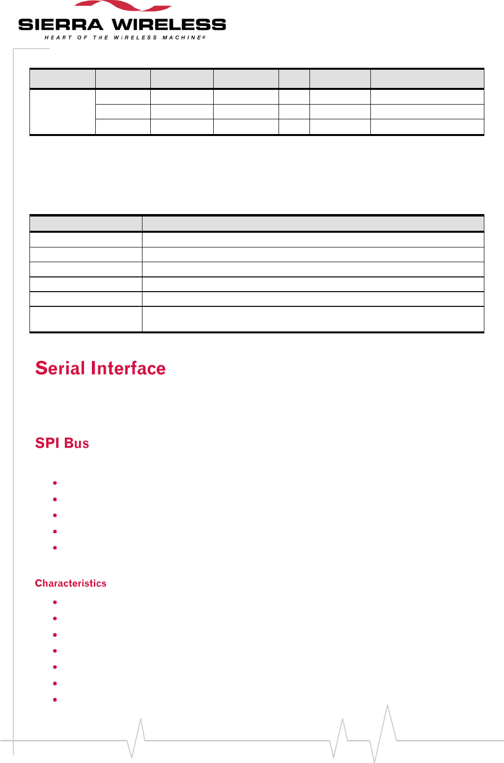
The Q26 Extreme Wireless CPU® provides two SPI bus (i.e. for LCD, memories…). or an I²C 2-wire
interface.
Both SPI bus interfaces include:
A CLK signal
An I/O signal
An I signal
A CS (Chip Select) signal complying with the standard SPI bus (any GPIO).
An optional Load signal (only the SPIx-LOAD signal)
Master mode operation
The CS signal must be any GPIO
The LOAD signal (optional) is used for the word handling mode (only the SPIx-LOAD signal)
SPI speed is from 102 kbit/s to 13 Mbit/s in master mode operation
3 or 4-wire interface(5-wire possible with the optional SPIx-LOAD signal)
SPI-mode configuration: 0 to 3
1 to 16 bits data length
WM_DEV_Q26EX_PTS_002 Rev 006 Page 30 of 112
Product Technical Specification and
Customer Design Guidelines
Table 13. SPI Configuration
Operation
Maximum
Speed
SPI-
Mode
Duplex
3-wire type
4-wire type
5-wire type
Master
13 Mb/s
0,1,2,3
Half
SPIx-CLK;
SPIx-IO;
GPIOx as CS
SPIx-CLK;
SPIx-IO;
SPIx-I;
GPIOx as CS
SPIx-CLK;
SPIx-IO;
SPIx-I;
GPIOx as CS;
SPIx-LOAD
(not muxed in GPIO);
For the 3-wire configuration, SPIx-I/O is used as input and output.
For the 4-wire configuration, SPIx-I/O is used as output only, SPIx-I is used as input only.
For the 5-wire configuration, SPIx-I/O is used as output only, SPIx-I is used as input only. And the dedicated SPIx-LOAD
signal is used. It is an additional signal in more than a Chip Select (any other GPIOx)
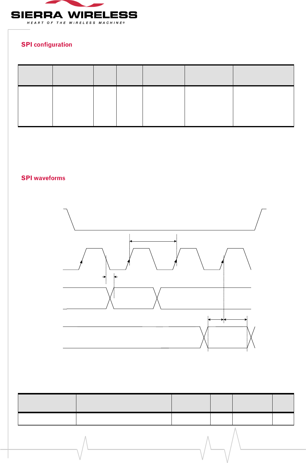
Waveforms for SPI transfer with 4-wire configuration in master mode 0.
Data-OUTdelay
CLK-cycle
Data-IN-hold
Data-IN-setup
SPIx-IO
Data valid
Data valid
SPIx-CLK
SPIx-I
GPIOx as CS
Figure 3. SPI Timing diagrams, Mode 0, Master, 4 wires
Table 14. AC characteristics
Signal
Description
Minimum
Typ
Maximum
Unit
CLK-cycle
SPI clock frequency
0.102
13
MHz
WM_DEV_Q26EX_PTS_002 Rev 006 Page 31 of 112
Product Technical Specification and
Customer Design Guidelines
Signal
Description
Minimum
Typ
Maximum
Unit
Data-OUT delay
Data out ready delay time
10
ns
Data-IN-setup
Data in setup time
2
ns
Data-OUT-hold
Data out hold time
2
ns
Waveforms for SPI transfer with the SPIx-LOAD signal configuration in master mode 0 (chip select is
not represented).
CLK-cycle
Tload_lead
SPIx-IO D1
SPIx-CLK
SPIx-LOAD
D0
Tload_high Tload_lag
Dx
Figure 4. SPI Timing diagrams with SPIx-LOAD signal, Mode 0, Master, 4 wires
Table 15. Pins description
Signal
Pin
number
I/O
I/O
type
Reset
state
Description
Multiplexed
with
SPI1-CLK
23
O
2V8
Z
SPI Serial Clock
GPIO28
SPI1-IO
25
I/O
2V8
Z
SPI Serial input/output
GPIO29
SPI1-I
24
I
2V8
Z
SPI Serial input
GPIO30
SPI1-LOAD
22
O
2V8
Z
SPI load
GPIO31
For Open drain, 2V8 and 1V8 voltage characteristics and Reset state definition refer to Chapter 3.3, "Electrical information for
digital I/O".
WM_DEV_Q26EX_PTS_002 Rev 006 Page 32 of 112
Product Technical Specification and
Customer Design Guidelines
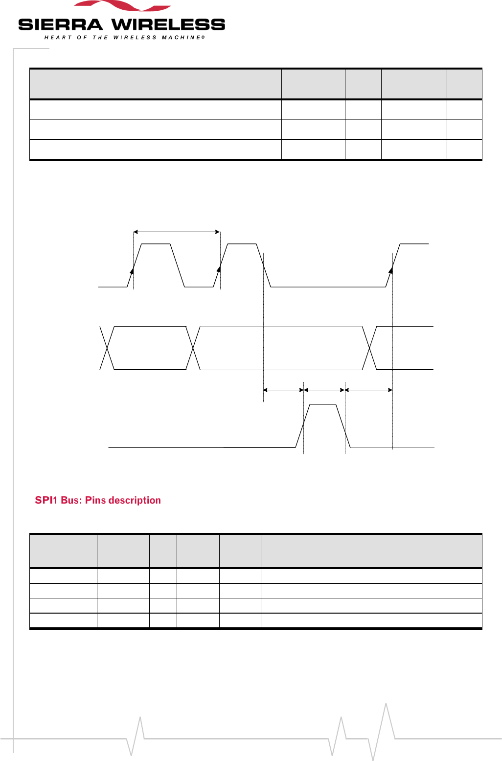
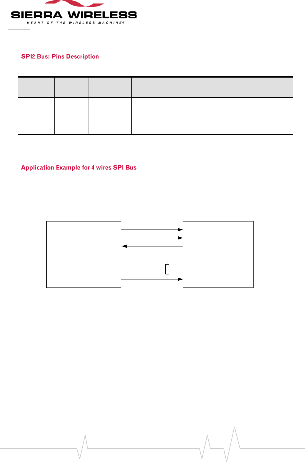
Table 16. Pins description
Signal
Pin
number
I/O
I/O
type
Reset
state
Description
Multiplexed
with
SPI2-CLK
26
O
2V8
Z
SPI Serial Clock
GPIO32
SPI2-IO
27
I/O
2V8
Z
SPI Serial input/output
GPIO33
SP2-I
29
I
2V8
Z
SPI Serial input
GPIO34
SPI2-LOAD
28
O
2V8
Z
SPI Load
GPIO35
See Chapter 3.3 “Electrical information for digital I/O” for Open drain, 2V8 and 1V8 voltage characteristics and Reset state
definition.
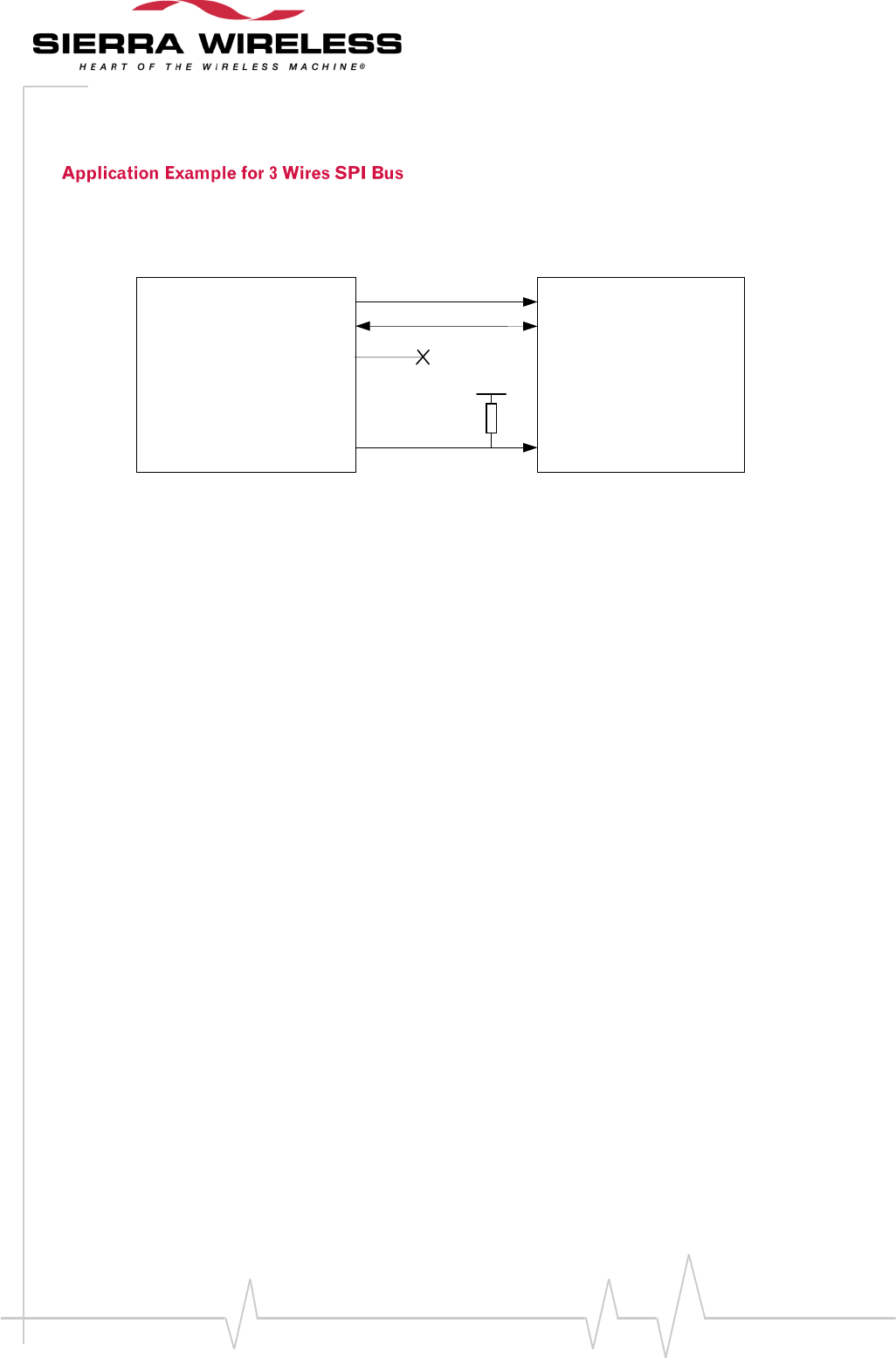
The specific feature of 4-wire serial interface (SPI bus) in which the input and output data lines are
disassociated. The SPIx-IO signal is used only for ouput data whereas the SPIx-I signal is used only
for input data.
Figure 5. Example of 4-wire SPI bus application
One pull-up resistor R1 is needed to set the SPIx-CS level for the reset state. R1 recommended value:
100kohm.
Except for R1, no external components are needed if the electrical specification of the customer
application complies with the Q26 Extreme Wireless CPU® SPIx interface electrical specification.
Customer
application
Q26 Extreme
Wireless CPU®
SPIx-IO
SPIx-CLK
~SPIx-LOAD
VCC_2V8
R1
SPIx-I
WM_DEV_Q26EX_PTS_002 Rev 006 Page 33 of 112
Product Technical Specification and
Customer Design Guidelines
The specific feature of 3-wire serial interface (SPI bus) in which the input and output data lines are
disassociated. The SPIx-IO signal is used for both output and input data.
Figure 6. Example of 3-wire SPI bus application
One pull-up resistor R1 is needed to set the SPIx-CS level for the reset state. R1 value depends on the
peripheral plugged on the SPIx interface. R1 recommended value: 100kohm.
Except for R1, no external components are needed if the electrical specification of the customer
application complies with the Q26 Extreme Wireless CPU® SPIx interface electrical specification.
The SPIx-I line is not used in 4-wire configuration. This line can be left open or used as GPIO for other
application’s functionality.
The SPIx interface voltage range is 2.8V. It can be powered either by VCC_2V8 (pin 10) of the Q26
Extreme Wireless CPU or by any other power supply.
Customer
application
Q26 Extreme
Wireless CPU®
SPIx-IO
SPIx-CLK
~SPIx-LOAD
VCC_2V8
R1
nc-SPIx-I
WM_DEV_Q26EX_PTS_002 Rev 006 Page 34 of 112
Product Technical Specification and
Customer Design Guidelines
The I2C interface includes a clock signal (SCL1) and data signal (SDA1) complying with a 100kbit/s-
standard interface (standard mode: s-mode).
The I²C bus is always master.
The maximum speed transfer range is 400kbit/s (fast mode: f-mode).
I²C bus waveform in master mode configuration:
SCL-freq
T-free
SDA1
SCL1
Data valid Data valid
T-start T-data hold T-data setup
T-high
T-stop
Figure 7. I²C Timing diagrams, Master
Table 17. AC characteristics
Signal
Description
Minimum
Typ
Maximum
Unit
SCL1-freq
I²C clock frequency
100
400
kHz
T-start
Hold time START condition
0.6
µs
T-stop
Setup time STOP condition
0.6
µs
T-free
Bus free time, STOP to START
1.3
µs
T-high
High period for clock
0.6
µs
T-data-hold
Data hold time
0
0.9
µs
T-data-setup
Data setup time
100
ns
WM_DEV_Q26EX_PTS_002 Rev 006 Page 35 of 112
Product Technical Specification and
Customer Design Guidelines
Table 18. Pin description
Signal
Pin
number
I/O
I/O type
Reset
state
Description
Multiplexed
with
SCL1
44
O
Open drain
Z
Serial Clock
GPIO26
SDA1
46
I/O
Open drain
Z
Serial Data
GPIO27
See Chapter Caution:, "Electrical information for digital I/O” for Open drain, 2V8 and 1V8 voltage characteristics and Reset
state definition.
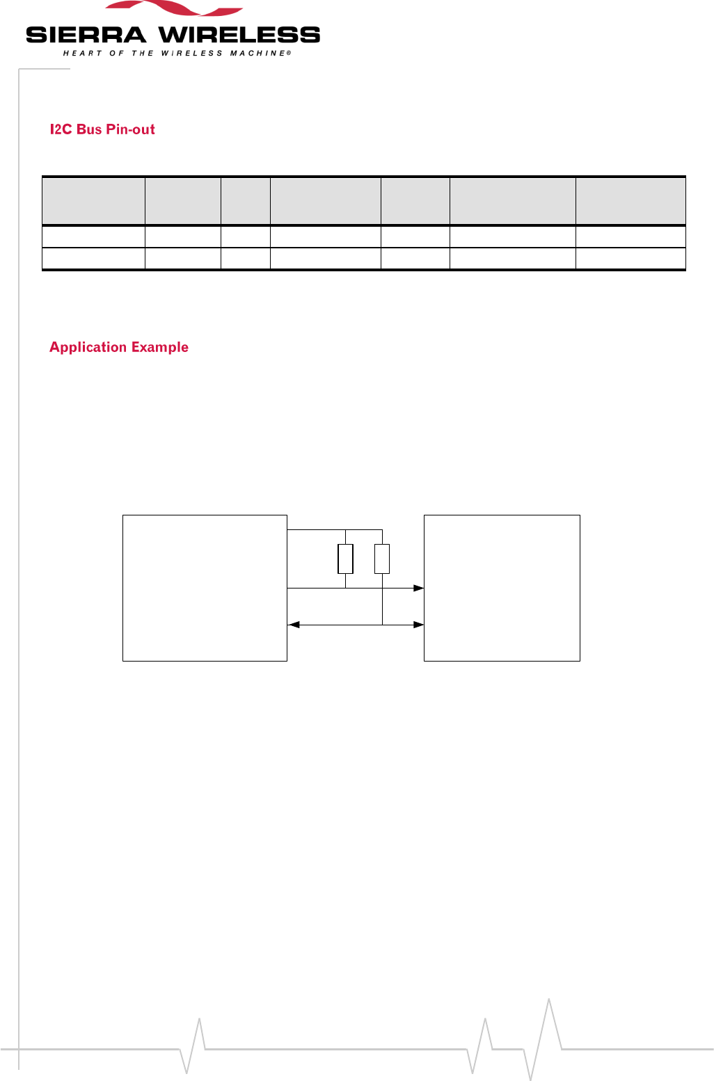
The two lines need to be pulled-up to the V_I²C voltage. The V_I²C voltage is dependent on the
customer application component connected on the I²C bus. Nevertheless, the VI²C must comply with
the Q26 Extreme Wireless CPU® electrical specification.
The VCC_2V8 (pin 10) of the Q26 Extreme Wireless CPU® may be used to connect the pull-up
resistors, if the I²C bus voltage is 2.8 V.
Customer
application
Q26 Extreme
Wireless CPU®
SDA1
SCL1
1k 1k
VCC_2V8
Figure 8. Example of I²C bus application
The pull-up resistor values are selected depending on the mode used. For the Fast mode, it is
recommended to use 1kohm resistor in order to ensure the compliance with the I²C specification. For
the Standard mode, higher values of resistors may be used to save power consumption.
WM_DEV_Q26EX_PTS_002 Rev 006 Page 36 of 112
Product Technical Specification and
Customer Design Guidelines
The Q26 Extreme Wireless CPU® offers a 16 bits parallel and 1V8 bus interface. Its characteristics are
described below:
Up to 128 Mega Byte address range per chip select (CS2 and CS3),
Support for 8, 16, and 32 bit (multiplexed synchronous mode) devices,
Byte enable signals for 16 bit and 32 bits operation,
Fully programmable timings based on AHB (a division of the ARM clock at 26 MHz ) cycles
(except for synchronous mode which is based on CLKBURST cycles at 26 MHz only),
individually selectable timings for read and write,
0 to 7 clock cycles for setup,
1 to 32 clock cycles for access cycle,
1 to 8 clock cycles for page access cycle,
0 to 7 clock cycles for hold,
1 to 15 clock cycles for turnaround.
Page mode Flash memory support,
page size of 4, 8, 16 or 32,
Burst mode Flash memory support up to AHB (26 MHz) clock frequency (for devices
sensitive to rising edge of the clock only)
AHB, AHB/2, AHB/4 or AHB/8 burst clock output
burst size of 4, 8, 16, 32,
automatic CLKBURST power-down between accesses,
Intel mode (WE and OE) and Motorola mode (E and R/W) control signals,
Synchronous write mode,
Synchronous multiplexed data/address mode (x32 mode),
Adaptation to word, halfword, and byte accesses to the external devices.
WM_DEV_Q26EX_PTS_002 Rev 006 Page 37 of 112
Product Technical Specification and
Customer Design Guidelines
Table 19. Pinout Definitions
Signal
Pin
number
Reset
state
I/O
I/O
type
Description
Multiplexed
with
D0
85
Pull down
I/O
1V8
Bidirectional data and address line
Not mux
D1
87
Pull down
I/O
1V8
Bidirectional data and address line
Not mux
D2
89
Pull down
I/O
1V8
Bidirectional data and address line
Not mux
D3
91
Pull down
I/O
1V8
Bidirectional data and address line
Not mux
D4
93
Pull down
I/O
1V8
Bidirectional data and address line
Not mux
D5
95
Pull down
I/O
1V8
Bidirectional data and address line
Not mux
D6
97
Pull down
I/O
1V8
Bidirectional data and address line
Not mux
D7
99
Pull down
I/O
1V8
Bidirectional data and address line
Not mux
D8
100
Pull down
I/O
1V8
Bidirectional data and address line
Not mux
D9
98
Pull down
I/O
1V8
Bidirectional data and address line
Not mux
D10
96
Pull down
I/O
1V8
Bidirectional data and address line
Not mux
D11
94
Pull down
I/O
1V8
Bidirectional data and address line
Not mux
D12
92
Pull down
I/O
1V8
Bidirectional data and address line
Not mux
D13
90
Pull down
I/O
1V8
Bidirectional data and address line
Not mux
D14
88
Pull down
I/O
1V8
Bidirectional data and address line
Not mux
D15
86
Pull down
I/O
1V8
Bidirectional data and address line
Not mux
~OE-
R/W
81
1
O
1V8
Output enable signal (Intel mode);
read not write signal (Motorola mode)
Not mux
~WE-E
84
1
O
1V8
Write enable Signal (Intel mode)
Enable signal (Motorola mode)
Not mux
~CS3
83
Pull up
I/O
1V8
User Chip select 3
GPIO44
~CS2
51
Pull up
I/O
1V8
User Chip Select 2
GPIO1/INT2
A1
42
1
O
1V8
This signal has 2 functions:
external Address or byte enable 2 for
16 or 32 bits devices.
An other name is used : A1_BE2
Not mux
A24
53
Z
I/O
1V8
Address line for external device /
Command selection
GPIO2
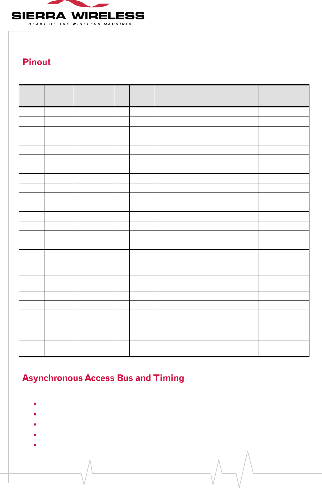
For all timing diagrams in the following section the notations here after are used:
ADR is used for address bus A [24,1] or D [15:0].when used as address lines.
DATA is used for D[15:0] when used as DATA lines
~CS is used for ~CS2 or~CS3.
~BE is used for A1_~BE2 (Double function on A1 pin).
~OE and R/W are used for ~OE_R/W
WM_DEV_Q26EX_PTS_002 Rev 006 Page 38 of 112
Product Technical Specification and
Customer Design Guidelines
~WE and E are used for ~WE_E
~ADV signal (Not available on 100 pins connector) is the address valid signal.
Figure 9. Asynchronous access
The ~ADV signal is mentioned here because synchronous mode devices may require the signal to be
asserted when an asynchronous access is performed.
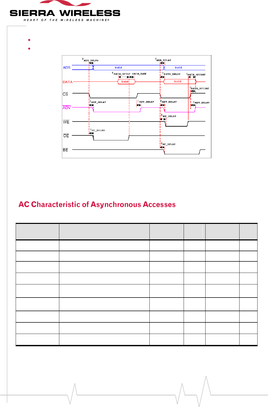
Table 20. AC Characteristic of Asynchronous Accesses
Signal
Description
Minimum
Typ
Maximum
Unit
TADR_DELAY
ADR delay time from ~CS active
3
ns
TDATA_SETUP
DATA to ~OE setup time
18
ns
TDATA_HOLD
DATA hold time after ~OE inactive
3
4
ns
TDATA_DELAY
DATA delay time from ~CS active
5
ns
TDATA_SECURE
DATA hold time after ~WE inactive or
~CS inactive
-5[1]
ns
TADV_DELAY
ADV delay time from ~CS active and
inactive
3
ns
TWE_DELAY
~WE delay time from ~CS active
3[2]
ns
TOE_DELAY
~OE delay time from ~CS active
3[2]
ns
TBE_DELAY
~BE delay time from ~CS active
3
ns
[1]This timing forces to program at least one cycle for asynchronous.
[2] These maximum delays depend also on setting of registers
WM_DEV_Q26EX_PTS_002 Rev 006 Page 39 of 112
Product Technical Specification and
Customer Design Guidelines
For all timing diagrams in the following section the notations here after are used:
ADR is used for address bus as A24, A1 or D [15:0].when used as address lines.
DATA is used for D [15:0]. when used as data lines.
~CS is used for ~CS2 or ~CS3.
~BE is used for A1_~BE2 (Double function on A1 pin).
~OE and R/W are used for ~OE_R/W.
~WE and E are used for ~WE_E
CLKBURST: is the internal clock at 26 MHz (Not available on connector pinout).
~ADV signal (Not available on 100 pins connector) is the address valid signal.
~BAA: signal (Not available on 100 pins connector): is the burst address advance for
synchronous operations.
~WAIT signal (Not available on 100 pins connector): is the wait signal for synchronous
operation.
WM_DEV_Q26EX_PTS_002 Rev 006 Page 40 of 112
Product Technical Specification and
Customer Design Guidelines
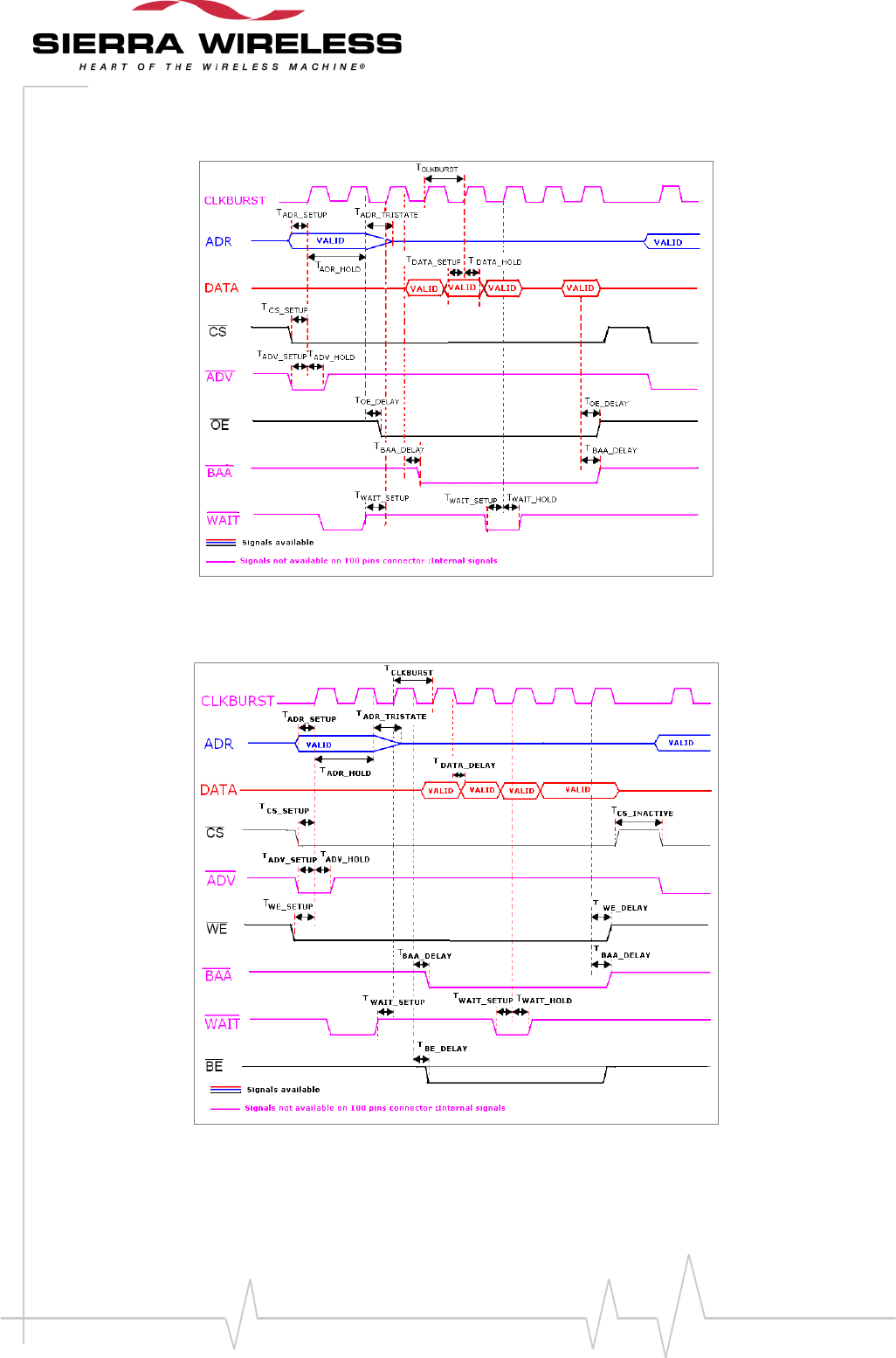
Figure 10. Read synchronous timing
Figure 11. Write synchronous timing
WM_DEV_Q26EX_PTS_002 Rev 006 Page 41 of 112
Product Technical Specification and
Customer Design Guidelines
Table 21. AC Characteristic of Asynchronous Accesses
Signal
Description
Minimum
Typ
Maximum
Unit
TDATA_DELAY
CLKBURTS falling edge to DATA valid
delay
4
ns
TWE_SETUP
WE to CLKBURST setup time
7
ns
TBE_DELAY
CLKBURST falling edge to BE delay
4
ns
TCLKBURST
CLKBURST clock : period time
38.4
ns
TADR_SETUP
Address bus setup time
7
ns
TADR_HOLD
Address bus hold time
19
ns
TADR_TRISTATE
Address bus tristate time
10
ns
TDATA_SETUP
Data bus setup time
5
ns
TDATA_HOLD
Data bus hold time
3
ns
TCS_SETUP
Chip select setup time
7
ns
TADV_SETUP
ADV setup time
7
ns
TADV_HOLD
ADV hold time
7
ns
TOE_DELAY
Output Enable delay time
13
ns
TBAA_DELAY
BAA delay time
13
ns
TWAIT_SETUP
Wait setup time
5
ns
TWAIT_HOLD
Wait hold time
5
ns
WM_DEV_Q26EX_PTS_002 Rev 006 Page 42 of 112
Product Technical Specification and
Customer Design Guidelines
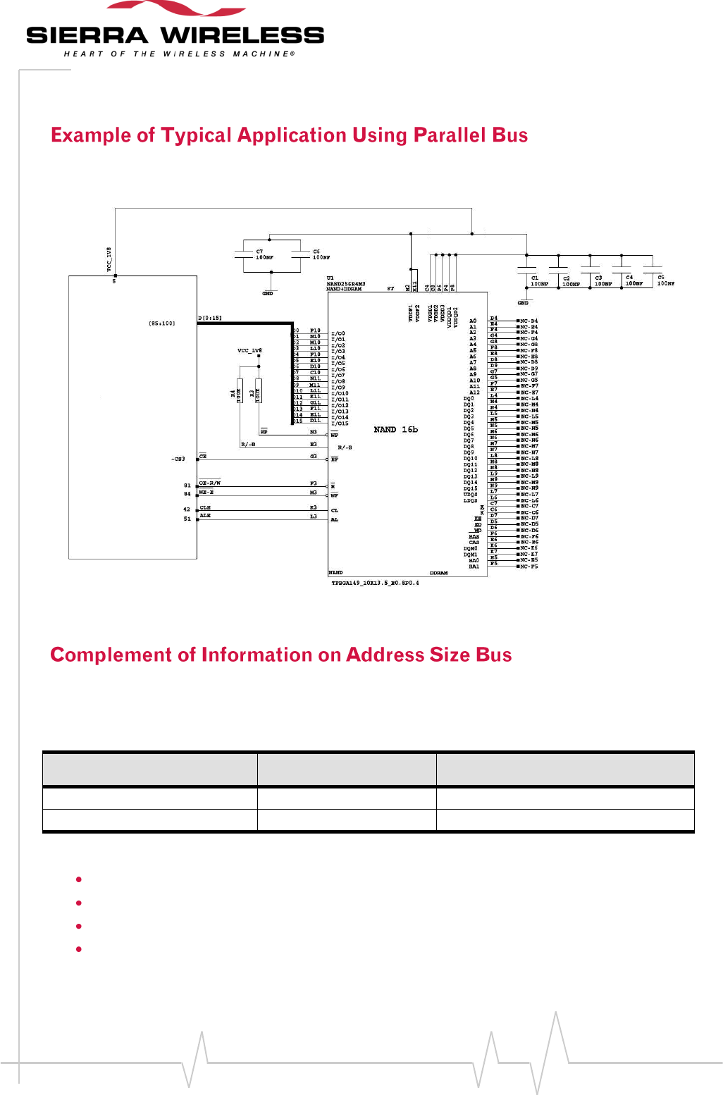
For example, it is possible to interface an NAND memory.
Figure 12. Example of parallel bus application (NAND)
The following table lists the possible configurations depending on address bus size requested on
parallel interface.
Table 22. Address bus size details
Address bus size
Address lines
Chip select available
1
A1
/CS2, /CS3
2
A1, A24
/CS2, /CS3
Few signals are multiplexed. It is thus possible to have these configurations.
~CS3*, A1, GPIO2
~CS3*, A1, A24,
~CS3*, ~CS2*, A1, GPIO2
~CS3*, ~CS2*, A1, A24
Q26 Extrene
WM_DEV_Q26EX_PTS_002 Rev 006 Page 43 of 112
Product Technical Specification and
Customer Design Guidelines
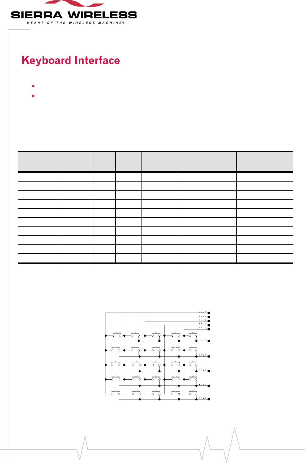
This interface provides 10 connections:
5 rows (ROW0 to ROW4) and
5 columns (COL0 to COL4).
The scanning is a digital one and debouncing is performed in the Q26 Extreme Wireless CPU®.
No discrete components such as Rs, Cs (Resistors, Capacitors) are needed.
Table 23. Keyboard interface pin description
Signal
Pin
number
I/O
I/O
type
Reset
state
Description
Multiplexed with
ROW0
68
I/O
1V8
0
Row scan
GPIO9
ROW1
67
I/O
1V8
0
Row scan
GPIO10
ROW2
66
I/O
1V8
0
Row scan
GPIO11
ROW3
65
I/O
1V8
0
Row scan
GPIO12
ROW4
64
I/O
1V8
0
Row scan
GPIO13
COL0
59
I/O
1V8
Pull-up
Column scan
GPIO4
COL1
60
I/O
1V8
Pull-up
Column scan
GPIO5
COL2
61
I/O
1V8
Pull-up
Column scan
GPIO6
COL3
62
I/O
1V8
Pull-up
Column scan
GPIO7
COL4
63
I/O
1V8
Pull-up
Column scan
GPIO8
See Chapter Caution:, “Electrical information for digital I/O” for Open drain, 2V8 and 1V8 voltage characteristics and for
Reset state definition.
With the Open AT® Software, when the keyboard service is used, the whole multiplexed signals
become unavailable for other purposes. In the same way if one or more GPIOs (of this table) are
allocated the keyboard service is unavailable.
Figure 13. Example of keyboard implementation
WM_DEV_Q26EX_PTS_002 Rev 006 Page 44 of 112
Product Technical Specification and
Customer Design Guidelines
A flexible 8-wire serial interface is available, complying with V24 protocol signaling, but not with V28
(electrical interface) due to a 2.8 volts interface.
The signals are:
TX data (CT103-TX)
RX data (CT104-RX)
Request To Send (~CT105-RTS)
Clear To Send (~CT106-CTS)
Data Terminal Ready (~CT108-2-DTR)
Data Set Ready (~CT107-DSR).
Data Carrier Detect (~CT109-DCD)
Ring Indicator (CT125-RI).
Table 24. UART1 interface pin description
Signal
Pin
number
I/O
I/O
type
Reset state
Description
Multiplexed
with
CT103-TXD1*
71
I
2V8
Z
Transmit serial data
GPIO36
CT104-RXD1*
73
O
2V8
Z
Transmit serial data
GPIO37
~CT105-RTS1*
72
I
2V8
Z
Request To Send
GPIO38
~CT106-CTS1*
75
O
2V8
Z
Clear To Send
GPIO39
~CT107-DSR1*
74
O
2V8
Z
Data Set Ready
GPIO40
~CT108-2-DTR1*
76
I
2V8
Z
Data Terminal Ready
GPIO41
~CT109-DCD1 *
70
O
2V8
Undefined
Data Carrier Detect
GPIO43
~CT125-RI1 *
69
O
2V8
Undefined
Ring Indicator
GPIO42
CT102-GND*
Shielding
leads
GND
Ground
* See Chapter 3.3 Electrical information for digital I/O” for Open drain, 2V8 and 1V8 voltage characteristics and for the
reset state definition.
*According to PC view
With the Open AT® Software Suite, when the UART1 service is used, the whole multiplexed signals
become unavailable for other purposes. In the same way if one or more GPIOs (of this table) are
allocated the UART1 service is unavailable.
The rise and fall time of the reception signals (mainly CT103) must be less than 300 ns.
The maximum baud rate of UART1 is 921 kbit/s for the Open AT® Software Suite firmware.
Caution: The Q26 Extreme Wireless CPU® is designed to operate using all the serial interface signals. In
particular, it is mandatory to use RTS and CTS for hardware flow control in order to avoid data
loss/corruption during transmission.
The level shifter must be a 2.8V with V28 electrical signal compliant.
WM_DEV_Q26EX_PTS_002 Rev 006 Page 45 of 112
Product Technical Specification and
Customer Design Guidelines
Figure 14. Example of RS-232 level shifter implementation for UART1
U1 chip also protects the Wireless CPU against ESD at 15kV. (Air Discharge)
Recommended Components:
R1, R2: 15kohm
C1, C2, C3, C4, C5: 1uF
C6: 100nF
C7: 6.8uF TANTAL 10V CP32136 AVX
U1: ADM3307AECP Analog devices
J1: SUB-D9 female
R1 and R2 are necessary only during Reset state, to force the ~CT1125-RI1 and ~CT109-DCD1 signal to
high levels.
The ADM3307AECP chip has a maximum speed of 921kbits/s. If other level shifters are used, ensure
that their speeds are compliant with the UART1 useful speed.
The ADM3307AECP can be powered either by VCC_2V8 (pin 10) of the Q26 Extreme Wireless CPU®
or by an external regulator at 2.8 volts.
If the UART1 interface is connected directly to a host processor, it is not necessary to use level shifters.
The interface can be connected as shown in the figure 15.
Q26 Extrene
WM_DEV_Q26EX_PTS_002 Rev 006 Page 46 of 112
Product Technical Specification and
Customer Design Guidelines
V24/CMOS possible design:
Customer application
( DTE )
Q26 Extreme
Wireless CPU
( DCE )
GND
~RESET
ON / ~OFF
CT103-TXD1 / GPIO36
CT104-RXD1 / GPIO37
~CT105-RTS1 / GPIO38
~CT106-CTS1 / GOPI39
19
75
72
73
18
71
Shielding
Rx
RTS
CTS
GND
Tx
Figure 15. Example of V24/CMOS serial link implementation for UART1
The design shown in the above figure is a basic design type.
However, a more flexible design to access this serial link with all the modem signals is shown below:
Customer application
( DTE )
Q26 Extreme
Wireless CPU
( DCE )
GND
~RESET
ON / ~OFF
~CT107-DSR1 / GPIO40
~CT109-DCD1 / GPIO43
~CT108-2-DTR1 / GPIO41
~CT125-RI1 / GPIO42
19
69
76
70
18
74
Shielding
DCD
DTR
RI
GND
DSR
CT103-TXD1 / GPIO36
CT104-RXD1 / GPIO37
~CT105-RTS1 / GPIO38
~CT106-CTS1 / GOPI39
75
72
73
71
Rx
RTS
CTS
Tx
2x 15k
2.8Volt
Figure 16. Example of full modem V24/CMOS serial link implementation for UART1
It is recommended to add 15kohm pull-up resistor on ~CT125-RI1 and ~CT109-DCD1 to set high level
for reset state.
The UART1 interface is a 2.8 volts type. Moreover, it is 3.3 volts tolerant.
For use with 5-wire serial interface
Signal: CT103-TXD1*, CT104-RXD1*, ~CT105-RTS1*, ~CT106-CTS1*
WM_DEV_Q26EX_PTS_002 Rev 006 Page 47 of 112
Product Technical Specification and
Customer Design Guidelines
The signal ~CT108-2-DTR1* must be managed by following the V24 protocol signaling, if you
want to use the slow idle mode.
Other signals and their multiplexes are not available.
Please refer to technical appendixes of AT Commands Manual [5] for more information.
For use with 4-wire serial interface
CT103-TXD1*, CT104-RXD1*, ~CT105-RTS1*, ~CT106-CTS1*
The signal ~CT108-2-DTR1* must be configured at low level.
Other signals and their multiplexes are not available.
Please refer to technical appendixes in the AT Commands Manual [5] for more information.
For use with 2-wire serial interface
This case is possible for connected external chip, but not recommended (and forbidden for AT
command or modem use)
The flow control mechanism has to be managed at the customer side.
CT103-TXD1*, CT104-RXD1*
The signal ~CT108-2-DTR1* must be configured at low level.
The signals ~CT105-RTS1*, ~CT106-CTS1* are not used, please configure the AT command
(AT+IFC=0,0 see AT command User Guide [5]).
The signal ~CT105-RTS1* must be configured at low level.
Other signals and their multiplexes are not available.
Please refer to technical appendixes in the AT Commands Manual [5] for more information.
An auxiliary serial interface (UART2) is available on Q26 Extreme Wireless CPU®. This interface may
be used to connect a Bluetooth or a GPS chip controlled by an Open AT® Plug-in.
Table 25. UART2 interface pin description
Signal
Pin
number
I/O
I/O type
Reset
state
Description
Multiplexed
with
CT103-TXD2*
31
I
1V8
Z
Transmit serial data
GPIO14
CT104-RXD2*
30
O
1V8
Z
Receive serial data
GPIO15
~CT106-CTS2*
32
O
1V8
Z
Clear To Send
GPIO16
~CT105-RTS2*
33
I
1V8
Z
Request To Send
GPIO17
See Chapter Caution:, “Electrical information for digital I/O” for Open drain, 2V8 and 1V8 voltage characteristics and Reset
state definition.
* According to PC view
WM_DEV_Q26EX_PTS_002 Rev 006 Page 48 of 112
Product Technical Specification and
Customer Design Guidelines
Caution: The Q26 Extreme Wireless CPU® UART2 is designed to operate using all the serial interface
signals. In particular, it is recommended to use RTS and CTS for hardware flow control in order
to avoid data corruption during transmission.
The maximum baud rate of UART2 is 921 kbit/s for the Open AT® Software Suite firmware.
The voltage level shifter must be a 1.8 volts with V28 electrical signal compliant.
Figure 17. Example of RS-232 level shifter implementation for UART2
Recommended components:
Capacitors
C1: 220nF
C2, C3, C4: 1μF
Inductor
L1: 10μH
RS-232 Transceivers
U1: LINEAR TECHNOLOGY LTC®2804IGN
J1: SUB-D9 female
The LTC2804 may be powered either by VCC_1V8 (pin 5) of the Q26 Extreme Wireless CPU® or by an
external regulator at 1.8 volts.
The UART2 interface may be connected directly to other components, if the voltage interface is 1.8V.
For use with 4-wire serial interface
CT103-TXD2*, CT104-RXD2*, ~CT105-RTS2*, ~CT106-CTS2*
The signal ~CT108-2-DTR2* must be configured at low level.
Other signals and their multiplexes are not available.
Q26 Extreme
WM_DEV_Q26EX_PTS_002 Rev 006 Page 49 of 112
Product Technical Specification and
Customer Design Guidelines
Please refer to technical appendixes in the AT Commands Manual [5] for more information.
For use with 2-wire serial interface
This case is possible for connected external chip, but not recommended (and forbidden for AT
command or modem use)
The flow control mechanism has to be managed at the customer side.
CT103-TXD2*, CT104-RXD2*
The signals ~CT105-RTS2*, ~CT106-CTS2* are not used, you must configure the AT command
(AT+IFC=0,0 see AT Commands Manual [5]).
The signal ~CT105-RTS2* must be configured at low level.
Other signals and their multiplexes are not available.
Please refer to technical appendixes in the AT Commands Manual [5] for more information.
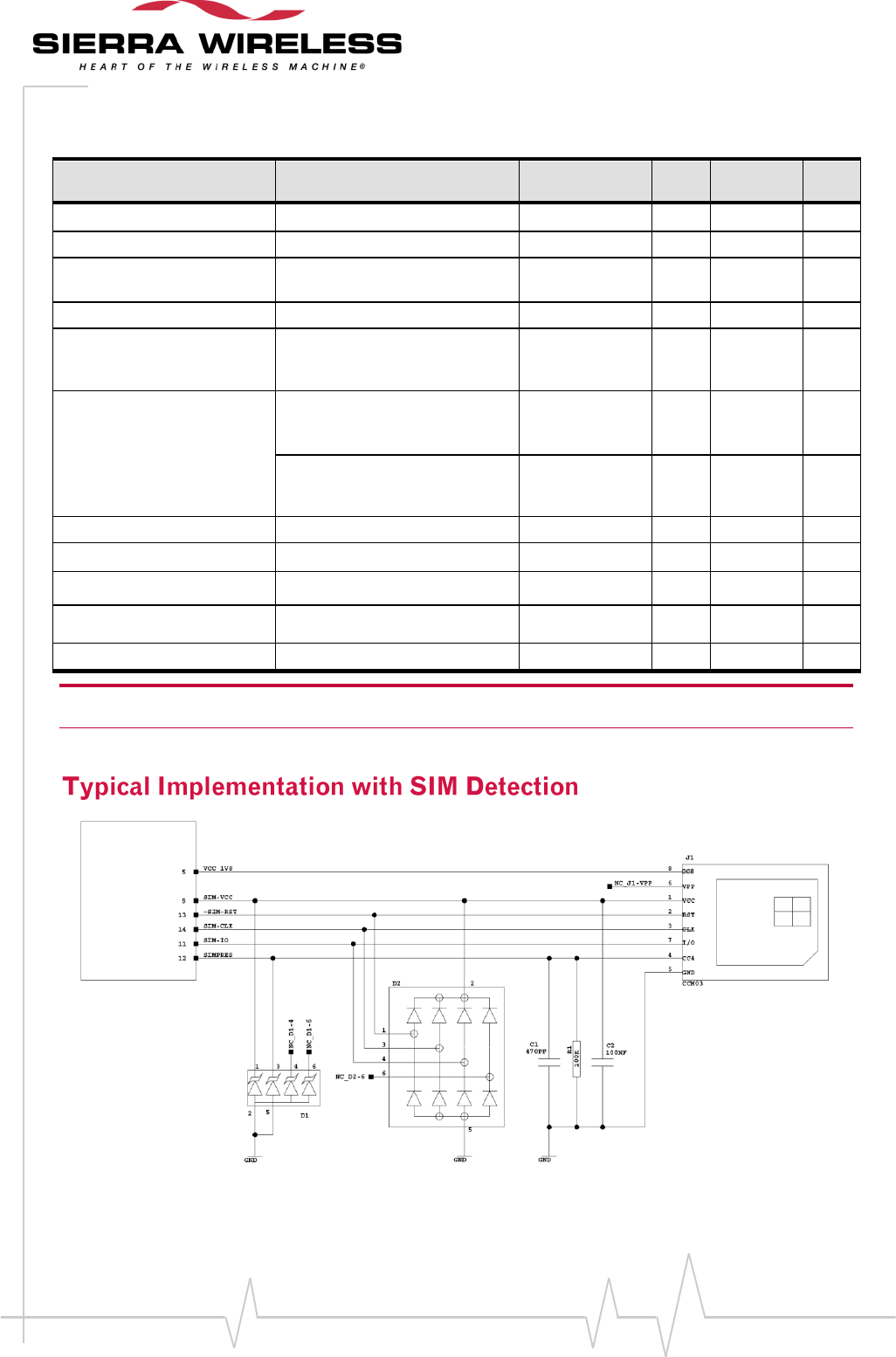
The Universal Subscriber Identification Module (USIM) may be directly connected to the Q26
Extreme Wireless CPU® via this dedicated interface. Using the USIM is recommended over the SIM
card.
The five signals are:
SIM-VCC: USIM power supply
~SIM-RST: reset
SIM-CLK: clock
SIM-IO: I/O port
SIMPRES: USIM card detect
The USIM interface controls a 1V8/3V USIM.
Table 26. USIM interface pin description
Signal
Pin
number
I/O
I/O type
Reset
state
Description
Multiplexed
with
SIM-CLK
14
O
2V9 / 1V8
0
USIM Clock
Not mux
~SIM-RST
13
O
2V9 / 1V8
0
USIM Reset
Not mux
SIM-IO
11
I/O
2V9 / 1V8
*Pull-up
USIM Data
Not mux
SIM-VCC
9
O
2V9 / 1V8
USIM Power
Supply
Not mux
SIMPRES
12
I
1V8
Z
USIM Card
Detect
GPIO18
*USIM-IO pull-up is about 10kohm
WM_DEV_Q26EX_PTS_002 Rev 006 Page 50 of 112
Product Technical Specification and
Customer Design Guidelines
* See Chapter 3.3 “Electrical information for digital I/O” for Open drain, 2V8 and 1V8 voltage characteristics and Reset
state definition.
WM_DEV_Q26EX_PTS_002 Rev 006 Page 51 of 112
Product Technical Specification and
Customer Design Guidelines
Table 27. USIM interface electrical characteristics
Parameter
Conditions
Minim.
Typ
Maxim.
Unit
SIM-IO VIH
IIH = ± 20µA
0.7xSIMVCC
V
SIM-IO VIL
IIL = 1mA
0.4
V
~SIM-RST, SIM-CLK
VOH
Source current = 20µA
0.9xSIMVCC
V
SIM-IO VOH
Source current = 20µA
0.8xSIMVCC
~SIM-RST, SIM-IO,
SIM-CLK
VOL
Sink current = -200µA
0.4
V
SIM-VCC Output Voltage
SIMVCC = 2.9V
IVCC= 1mA
2.84
2.9
2.96
V
SIMVCC = 1.8V
IVCC= 1mA
1.74
1.8
1.86
V
SIM-VCC current
VBATT = 3.8V
10
mA
SIM-CLK Rise/Fall Time
Loaded with 30pF
20
ns
~SIM-RST, Rise/Fall Time
Loaded with 30pF
20
ns
SIM-IO Rise/Fall Time
Loaded with 30pF
0.7
1
µs
SIM-CLK Frequency
Loaded with 30pF
3.25
MHz
Note: When SIMPRES is used, a low to high transition means that the USIM card is inserted and a high to
low transition means that the USIM card is removed.
Figure 18. Example of SIM Socket implementation
Q26 Extreme
WM_DEV_Q26EX_PTS_002 Rev 006 Page 52 of 112
Product Technical Specification and
Customer Design Guidelines
Recommended components:
R1: 100 kohm
C1: 470 pF
C2: 100 nF
D1: ESDA6V1SC6 from ST
D2: DALC208SC6 from SGS-THOMSON
J1: ITT CANNON CCM03 series
The capacitor (C2) placed on the SIM-VCC line must not exceed 330 nF.
Table 28. Pin description of the SIM socket
Signal
Pin number
Description
VCC
1
SIM-VCC
RST
2
~SIM-RST
CLK
3
SIM-CLK
CC4
4
SIMPRES with 100 k pull-down resistor
GND
5
GROUND
VPP
6
Not connected
I/O
7
SIM-IO
CC8
8
VCC_1V8 of Wireless CPU (pin 5)
WM_DEV_Q26EX_PTS_002 Rev 006 Page 53 of 112
Product Technical Specification and
Customer Design Guidelines
The Q26 Extreme Wireless CPU® provides up to 45 General Purpose I/Os, used to control any external
device such as an LCD or a Keyboard backlight.
Table 29. GPIO pin description
Signal
Pin
number
I/O
I/O type*
Reset state
Multiplexed with
GPIO0
43
I/O
2V8
Undefined
32kHz**
GPIO1
51
I/O
1V8
Pull-up
~CS2 / INT2
GPIO2
53
I/O
1V8
Z
A24
GPIO3
50
I/O
1V8
Z
INT0
GPIO4
59
I/O
1V8
Pull-up
COL0
GPIO5
60
I/O
1V8
Pull-up
COL1
GPIO6
61
I/O
1V8
Pull-up
COL2
GPIO7
62
I/O
1V8
Pull-up
COL3
GPIO8
63
I/O
1V8
Pull-up
COL4
GPIO9
68
I/O
1V8
0
ROW0
GPIO10
67
I/O
1V8
0
ROW1
GPIO11
66
I/O
1V8
0
ROW2
GPIO12
65
I/O
1V8
0
ROW3
GPIO13
64
I/O
1V8
0
ROW4
GPIO14
31
I/O
1V8
Z
CT103-TXD2
GPIO15
30
I/O
1V8
Z
CT104-RXD2
GPIO16
32
I/O
1V8
Z
~CT106-CTS2
GPIO17
33
I/O
1V8
Z
~CT105-RTS2
GPIO18
12
I/O
1V8
Z
SIMPRES
GPIO19
45
I/O
2V8
Z
Not mux
GPIO20
48
I/O
2V8
Undefined
Not mux
GPIO21
47
I/O
2V8
Undefined
Not mux
GPIO22
57
I/O
2V8
Z
Not mux*
GPIO23
55
I/O
2V8
Z
Not mux
GPIO24
58
I/O
2V8
Z
Not mux
GPIO25
49
I/O
2V8
Z
INT1
GPIO26
44
I/O
Open drain
Z
SCL1
WM_DEV_Q26EX_PTS_002 Rev 006 Page 54 of 112
Product Technical Specification and
Customer Design Guidelines
Signal
Pin
number
I/O
I/O type*
Reset state
Multiplexed with
GPIO27
46
I/O
Open drain
Z
SDA1
GPIO28
23
I/O
2V8
Z
SPI1-CLK
GPIO29
25
I/O
2V8
Z
SPI1-IO
GPIO30
24
I/O
2V8
Z
SP1-I
GPIO31
22
I/O
2V8
Z
SPI1_LOAD
GPIO32
26
I/O
2V8
Z
SPI2-CLK
GPIO33
27
I/O
2V8
Z
SPI2-IO
GPIO34
29
I/O
2V8
Z
SPI2-I
GPIO35
28
I/O
2V8
Z
SPI2_LOAD
GPIO36
71
I/O
2V8
Z
CT103-TXD1
GPIO37
73
I/O
2V8
1
CT104-RXD1
GPIO38
72
I/O
2V8
Z
~CT105-RTS1
GPIO39
75
I/O
2V8
Z
~CT106-CTS1
GPIO40
74
I/O
2V8
Z
~CT107-DSR1
GPIO41
76
I/O
2V8
Z
~CT108-2-DTR1
GPIO42
69
I/O
2V8
Undefined
~CT125-RI1
GPIO43
70
I/O
2V8
Undefined
~CT109-DCD1
GPIO44
83
I/O
2V8
Pull-up
PWM1 / ~CS3
See Chapter 3.3, “Electrical information for digital I/O” for Open drain, 2V8 and 1V8 voltage characteristics and Reset
state definition.
* If a Bluetooth module is used with the Q26 Extreme Wireless CPU®, these GPIOs must be reserved.
** With the Open AT® Software Suite see “AT Commands Manual ” [5].
Reset State:
0: Set to GND
1: Set to supply 1V8 or 2V8 depending on I/O type.
Pull-down: Internal pull-down with ~60k resistor.
Pull-up: Internal pull-up with ~60k resistor to supply 1V8 or 2V8 depending on I/O type.
Z: High impedance.
Undefined: caution, undefined must not be used in your application if a special state at
reset is needed. These pins may be of toggling signals.
Two Analog to Digital Converter inputs are provided by the Q26 Extreme Wireless CPU®. The
converters are more than 10-bit resolution, ranging from 0 volt to 2 volts.
WM_DEV_Q26EX_PTS_002 Rev 006 Page 55 of 112
Product Technical Specification and
Customer Design Guidelines
ADC1 / BAT-TEMP input can be used, typically, to monitor external temperature, useful for safety
power off in case of application over heating (for Li-Ion battery).
ADC2 input can be used for customer application.
Table 30. ADC pin description
Signal
Pin number
I/O
I/O type
Description
ADC1/BAT-TEMP*
20
I
Analog
A/D converter
ADC2
21
I
Analog
A/D converter
* This input can be used for a battery charging temperature sensor,
see Chapter 0, “Battery Charging interface“.
Table 31. ADC electrical characteristics
Parameter
Min
Typ
Max
Unit
Maximum output code
1635
LSB
Sampling period
0,5
3*
s
Input signal range
0
2
V
Input impedance
ADC1/BAT-TEMP
1M
ADC2
1M
*Sampling rate only for ADC2 and Open AT® application.
One Digital to Analog Converter (DAC) input is provided by the Wireless Microprocessor®.
The converter is 8-bit resolution, guaranteed monotonic with a range from 0V to 2.3V. This output
assumes a typical external load of 2k and 50pF in parallel to GND.
Table 32. Pin description of the DAC
Signal
Pin number
I/O
I/O type
Description
DAC0
82
O
Analog
D/A converter
Table 33. Electrical Characteristics of the DAC
Parameter
Min
Typ
Max
Unit
Resolution
-
8
-
bits
Maximum Output voltage
2.1
2.2
2.3
V
WM_DEV_Q26EX_PTS_002 Rev 006 Page 56 of 112
Product Technical Specification and
Customer Design Guidelines
Parameter
Min
Typ
Max
Unit
Minimum Output voltage
0
-
40
mV
Output voltage after reset
-
1.147
-
V
Integral Accuracy
-5
-
+5
LSB
Differential Accuracy
-1
-
+1
LSB
Full scale settling time
(load: 50pF // 2k to GND)
-
40
-
µs
One LSB settling time
(load: 50pF // 2k to GND )
-
8
-
µs
Two different microphone inputs and two different speaker outputs are supported. The Q26 Extreme
Wireless CPU® also includes an echo cancellation feature and noise reduction, which allows hands-
free function.
In some cases, ESD protection must be added on the audio interface lines.
The connection can be either differential or single-ended but using a differential connection in order
to reject common mode noise and TDMA noise is strongly recommended. When using a single-ended
connection, be sure to have a very good ground plane, a very good filtering as well as shielding in
order to avoid any disturbance on the audio path.
The gain of MIC inputs is internally adjusted and can be tuned using an AT command.
Both can be configured in differential or single ended.
The MIC2 inputs already include the biasing for an electret microphone allowing an easy connection.
By default, the MIC1 inputs are single-ended but it can be configured in differential.
The MIC1 inputs do not include an internal bias. The MIC1 input needs to have an external biasing if
an electret microphone is used.
AC coupling is already embedded in the Q26 Extreme Wireless CPU®.
WM_DEV_Q26EX_PTS_002 Rev 006 Page 57 of 112
Product Technical Specification and
Customer Design Guidelines
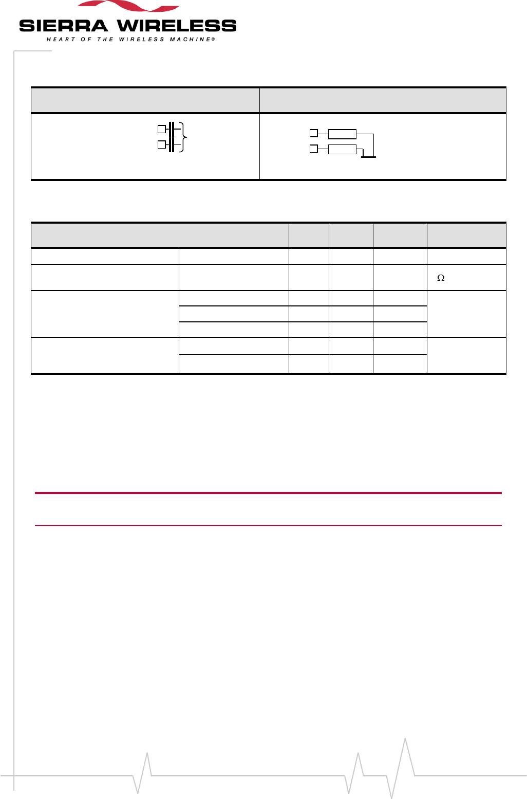
Table 34. Equivalent circuits of MIC1
DC equivalent circuit
AC equivalent circuit
Table 35. Electrical Characteristics of MIC1
Parameters
Min
Typ
Max
Unit
DC Characteristics
N/A
V
AC Characteristics
200 Hz < F < 4 kHz
Z1
70
120
160
k
Working voltage
(MIC1P-MIC1N)
AT+VGT*=3500(4)
13.8
18.6***
mVrms
AT+VGT*=2000(4)
77.5
104***
AT+VGT*=700(4)
346
465***
Maximum rating voltage
(MIC1P or MIC1N)
Positive
+7.35
V
Negative
-0.9
*The input voltage depends of the input micro gain set by AT command. Please refer to the document :AT command User
Guide [7]
**Because MIC2P is internally biased, it is necessary to use a coupling capacitor to connect an audio signal provided by
an active generator. Only a passive microphone can be directly connected to the MIC2P and MIC2N inputs.
*** This value is obtained with digital gain = 0 and for frequency = 1kHz :
(4) This value is given in dB, but it’s possible to toggle to index value. Please refer to the document :AT command User
Guide [7]
Warning: The voltage input value for MIC1 can’t exceed the maximum working
voltage, otherwise clipping will appear.
MIC1P
MIC1N
Z1
Z1
GND
MIC1P
MIC1N
DC
Blocked
WM_DEV_Q26EX_PTS_002 Rev 006 Page 58 of 112
Product Technical Specification and
Customer Design Guidelines
C5
40
38
Audio
ADC
100k Ohm
typ
100k Ohm
typ
100nF
100nF
MIC1P
MIC1N
VCC_2V8
(pin10)
R3
R2
R1
R4
C2
C3C1
L1
L2
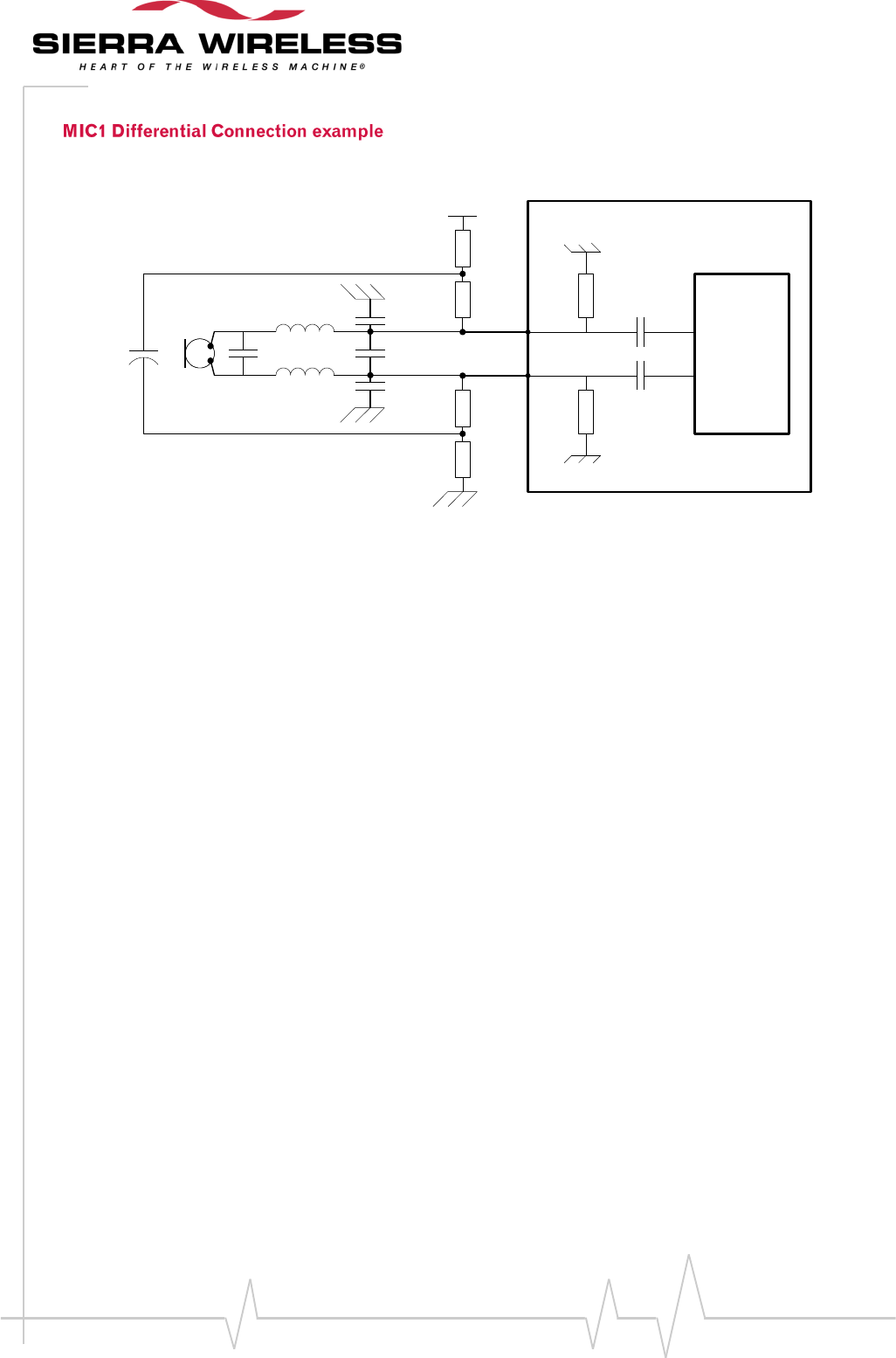
C4
MIC
Q26 Extreme
Figure 19. Example of MIC1 input differential connection with LC filter
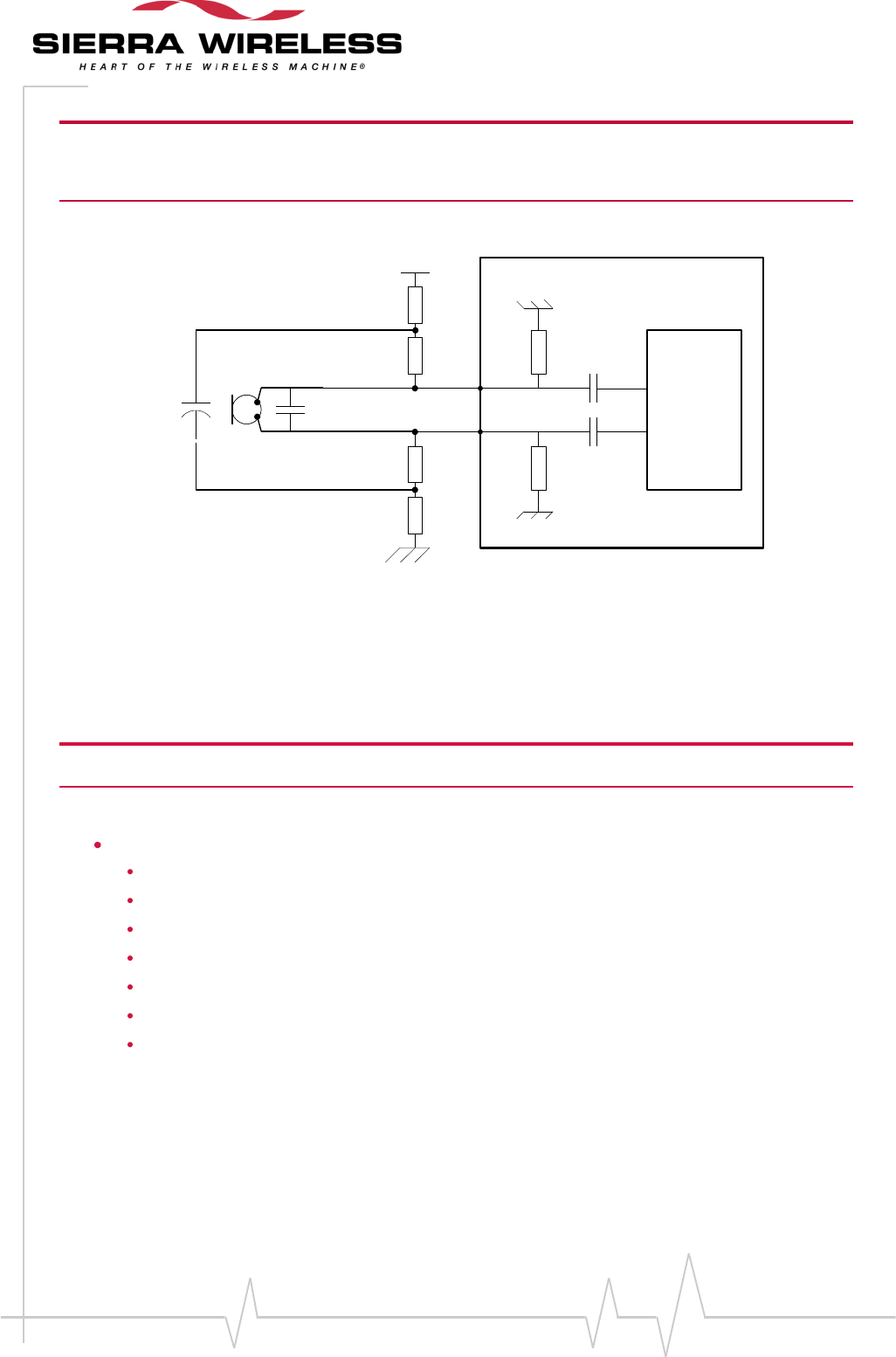
WM_DEV_Q26EX_PTS_002 Rev 006 Page 59 of 112
Product Technical Specification and
Customer Design Guidelines
Note: Depending on the design, audio quality may be good without L1, L2, C2, C3, and C4. Moreover, if
there is an EMI perturbation, this filter may reduce the TDMA noise. The filter (L1, L2, C2, C3, and C4)
is not mandatory. If this filter is not used, then the capacitor must be removed and the coil replaced
with 0 ohm resistors, as shown in the following diagram.
C5
40
38
Audio
ADC
100k Ohm
typ
100k Ohm
typ
100nF
100nF
MIC1P
MIC1N
VCC_2V8
(pin10)
R3
R2
R1
R4
C1
MIC
Q26 Extreme
Figure 20. Example of MIC1 input differential connection without LC filter
The capacitor C1 is highly recommended to eliminate the TDMA noise. C1 must be close to the
microphone.
Vbias may be VCC_2V8 (pin 10) of Q26 Extreme Wireless CPU®, but it is possible to use another 2
volts to 3 volts supply voltage depending on the micro characteristics.
Caution: If an external supply is used other than VCC_2V8 (pin 10), it is important to make sure that the
voltage is clean and free from noise, otherwise, the audio quality will be degraded.
Recommended components:
R1: 4.7kohm (for Vbias equal to 2.8V)
R2, R3: 820 ohm
R4: 1kohm
C1: 12pF to 33pF (need to be tuned, as per the design)
C2, C3, C4: 47pF ( need to be tuned as per the design)
C5: 2.2uF +/- 10%
L1, L2: 100nH (need to be tuned as per the design)
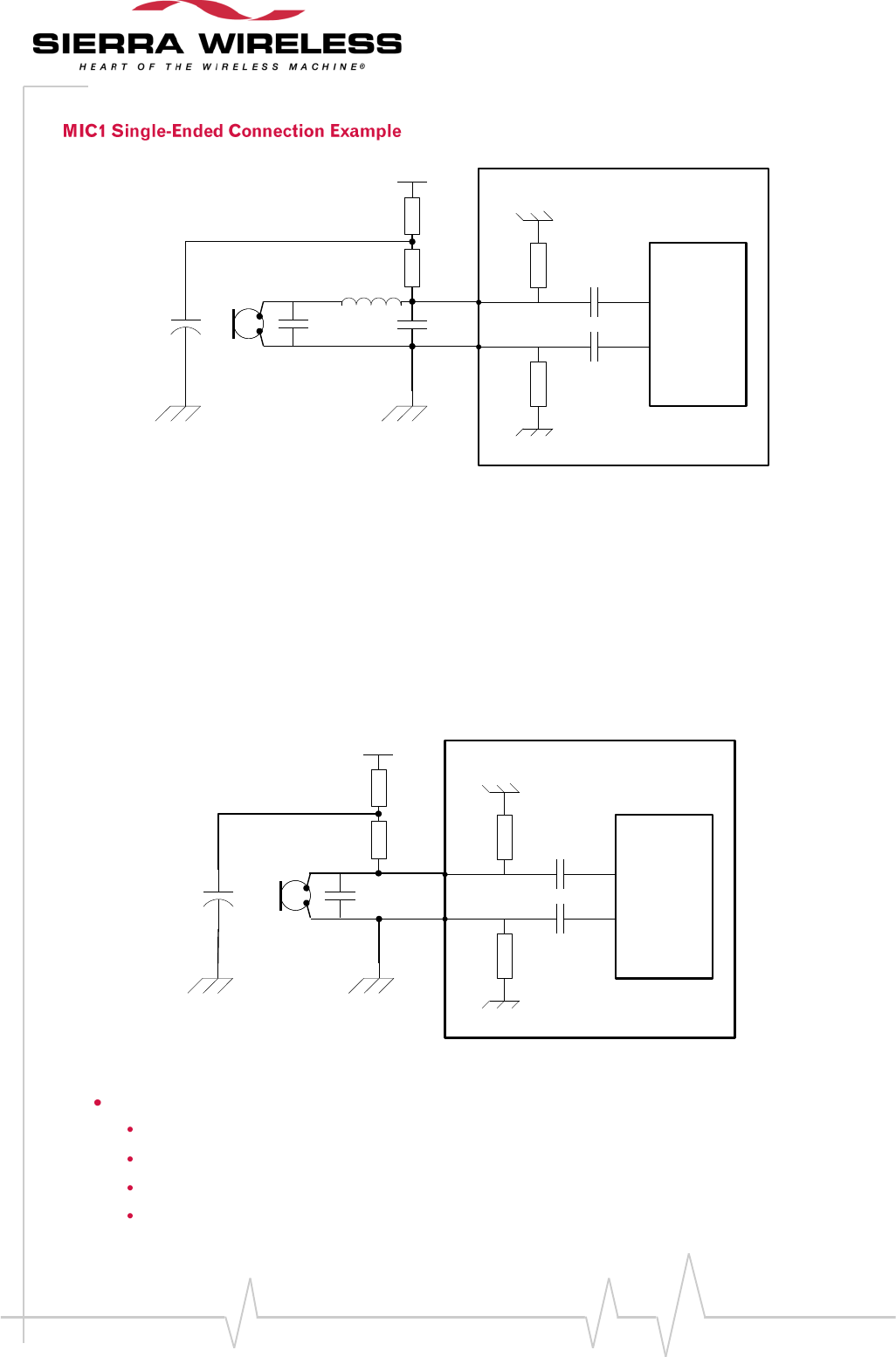
WM_DEV_Q26EX_PTS_002 Rev 006 Page 60 of 112
Product Technical Specification and
Customer Design Guidelines
L1
C2
C1
MIC
VCC_2V8
(pin10)
R2
R1
C5
Audio
ADC
100k Ohm
typ
100k Ohm
typ
100nF
100nF
MIC1P
MIC1N
40
38
Q26 Extreme
Figure 21. Example of MIC1 input single-ended connection with LC filter
The single-ended design is not recommended to improve TDMA noise rejection. Usually, it is difficult
to eliminate TDMA noise from a single-ended design.
It is recommended to add L1 and C2 footprint and a LC EMI filter, in order to eliminate the TDMA
noise.
When not used, the filter may be removed by replacing L1 with 0 ohm resistor and by disconnecting
C2, as shown in the following diagram.
C1MIC
VCC_2V8
(pin10)
R2
R1
C5
Audio
ADC
100k Ohm
typ
100k Ohm
typ
100nF
100nF
MIC1P
MIC1N
40
38
Q26 Extreme
Figure 22. Example of MIC1 input single-ended connection without LC filter
Recommended components:
R1: 4.7 kohm (for Vbias equal to 2.8V)
R2: 820 ohm
C1: 12pF to 33pF (need to tuned, as per the design)
C2: Must be tuned, as per the design.
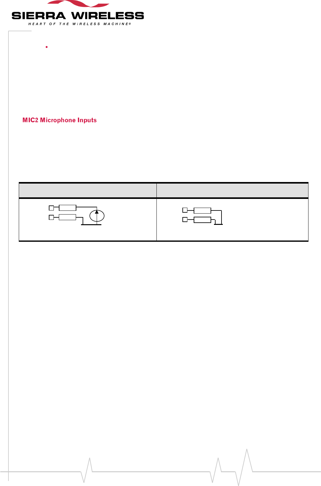
WM_DEV_Q26EX_PTS_002 Rev 006 Page 61 of 112
Product Technical Specification and
Customer Design Guidelines
L1: Must be tuned, as per the design.
Vbias must be very "clean" to avoid bad performance in case of single-ended implementation. It is
highly recommended to use the VCC_2V8 supply which is available on the system connector (pin 10),
in order to avoid this problem.
The capacitor C1 is highly recommended to eliminate the TDMA noise. C1 must be close to the
microphone.
By default, the MIC2 inputs are differential ones, but it can be configured in single ended. They
already include the convenient biasing for an electret microphone. The electret microphone can be
directly connected on those inputs, thus allowing easy connection to a handset.
AC coupling is already embedded in the Wireless CPU®.
Table 36. Equivalent circuits of MIC2
DC equivalent circuit
AC equivalent circuit
MIC2P
MIC2N
Z2
Z2
[G
ED
Re
fer
en
ce]
[G
ED
Re
fer
en
ce]
[G
ED
Re
fer
en
ce]
[G
ED
Re
fer
en
ce]
[G
ED
Re
fer
en
ce]
[G
ED
Re
fer
GND
[GED
Refere
nce]
[Rev]
[Date]
[GED
Refere
nce]
[Rev]
[Date]
[GED
Refere
nce]
[Rev]
[Date]
[GED
Refere
nce]
[Rev]
[Date]
MIC2+
[GED
Referen
ce]
[GED
Referen
ce]
[GED
Referen
ce]
[GED
Referen
ce]
[GED
Referen
ce]
[GED
Referen
MIC2P
MIC2N
R2
R2
GND
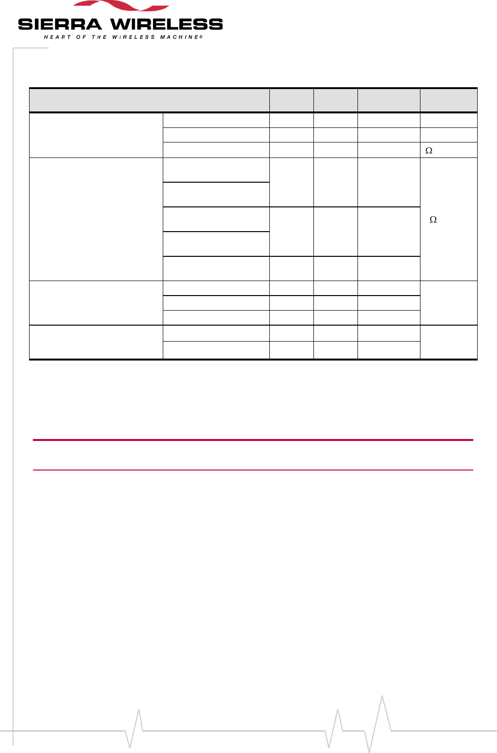
WM_DEV_Q26EX_PTS_002 Rev 006 Page 62 of 112
Product Technical Specification and
Customer Design Guidelines
Table 37. Electrical Characteristics of MIC2
Parameters
Min
Typ
Max
Unit
Internal biasing
DC Characteristics
MIC2+
2
2.1
2.2
V
Output current
0.5
1.5
mA
R2
1650
1900
2150
AC Characteristics
200 Hz<F<4 kHz
Z2 MIC2P
(MIC2N=Open)
1.1
1.3
1.6
k
Z2 MIC2N
(MIC2P=Open)
Z2 MIC2P
(MIC2N=GND)
0.9
1.1
1.4
Z2 MIC2N
(MIC2P=GND)
Impedance between
MIC2P and MIC2N
1.3
1.6
2
Working voltage
(MIC2P-MIC2N)
AT+VGT*=3500(4)
13.8
18.6 ***
mVrms
AT+VGT*=2000(4)
77.5
104***
AT+VGT*=700(4)
346
466***
Maximum rating voltage
(MIC2P or MIC2N)
Positive
+7.35**
V
Negative
-0.9
*The input voltage depends of the input micro gain set by AT command. Please refer to the document : AT command User
Guide[7]
**Because MIC2P is internally biased, it is necessary to use a coupling capacitor to connect an audio signal provided by an
active generator. Only a passive microphone can be directly connected to the MIC2P and MIC2N inputs.
*** This value is obtained with digital gain = 0 and for frequency = 1kHz ..
(4) This value is given in dB, but it’s possible to toggle to index value. Please refer to the document :AT Command Manual [7]
Warning: WARNING: The voltage input value for MIC2 can’t exceed the
maximum working voltage, otherwise clipping will appear.
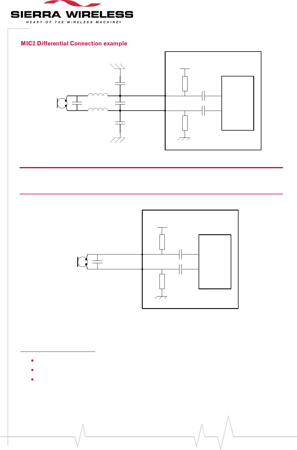
WM_DEV_Q26EX_PTS_002 Rev 006 Page 63 of 112
Product Technical Specification and
Customer Design Guidelines
C1
MIC
36
34
Audio
ADC
1350 Ohm
typ
1350 Ohm
typ
1.2V typ
100nF
100nF
MIC2P
MIC2N
C2
C3
C4
L1
L2
Q26 Extreme
Figure 23. Example of MIC2 input differential connection with LC filter
Note: Depending on the design, the audio quality may be good without L1, L2, C2, C3, and C4. Moreover, if
there is an EMI perturbation, this filter may reduce the TDMA noise. This filter (L1, L2, C2, C3, and C4)
is not mandatory. If this filter is not used, then capacitor must be removed and the coil replaced with 0
ohm resistors, as shown in the following diagram.
C1
MIC 36
34
Audio
ADC
1350 Ohm
typ
1350 Ohm
typ
1.2V typ
100nF
100nF
MIC2P
MIC2N
Q26 Extreme
Figure 24. Example of MIC2 input differential connection without LC filter
The capacitor C1 is highly recommended to eliminate the TDMA noise. C1 must be close to the
microphone.
Recommended components:
C1: 12pF to 33pF (need to be tuned as per the design )
C2, C3, C4: 47pF (need to be tuned as per the design)
L1, L2: 100nH (need to be tuned as per the design)
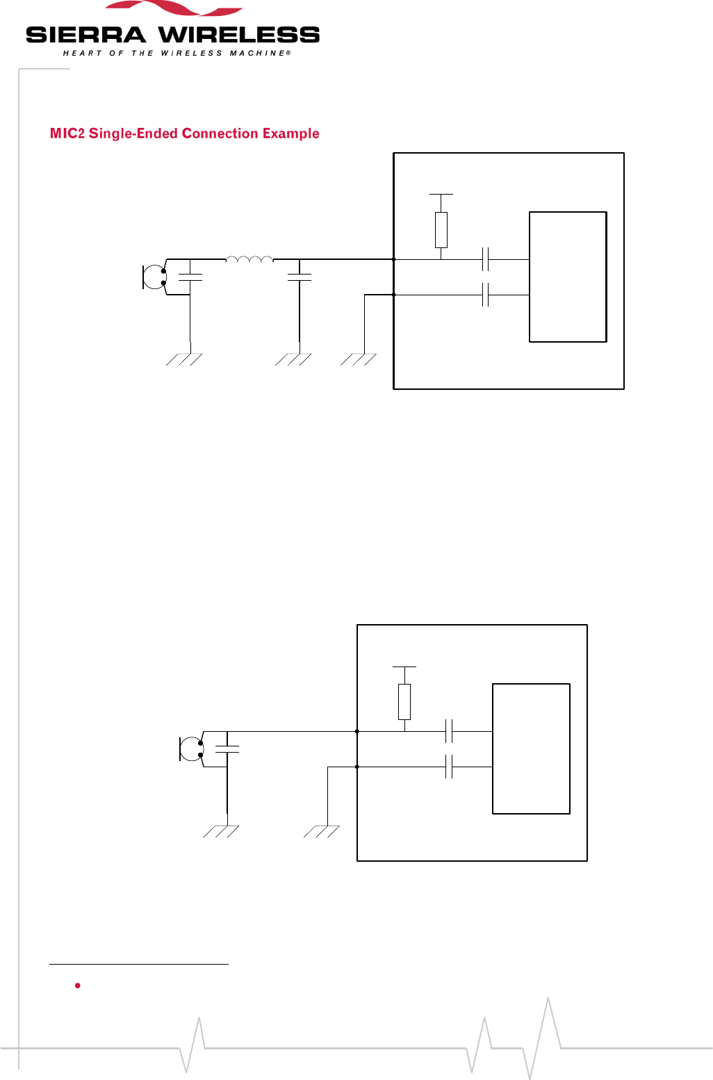
WM_DEV_Q26EX_PTS_002 Rev 006 Page 64 of 112
Product Technical Specification and
Customer Design Guidelines
36
34
C1MIC
Audio
ADC
1150 Ohm
typ
1.2V typ
100nF
100nF
MIC2P
MIC2N
L1
C2
Q26
Extreme
Figure 25. Example of MIC2 input single-ended connection with LC filter
The internal input resistor value becomes 1150 ohm, due to the connection of MIC2N to the ground
plane.
The single-ended design is not recommended to improve TDMA noise rejection. Usually, it is difficult
to eliminate TDMA noise from a single-ended design.
It is recommended to add L1, C2 footprint and a LC filter, in order to eliminate the TDMA noise.
When not used, the filter can be removed by replacing L1 with a 0 ohm resistor and by disconnecting
C2, as shown in the following diagram.
36
34
C1MIC
Audio
ADC
1150 Ohm
typ
1.2V typ
100nF
100nF
MIC2P
MIC2N
Q26
Extreme
Figure 26. Example of MIC2 input single-ended connection without LC filter
The capacitor C1 is highly recommended to eliminate the TDMA noise. C1 must be close to the
microphone.
Recommended components:
C1: 12pF to 33pF (need to be tuned, as per the design)
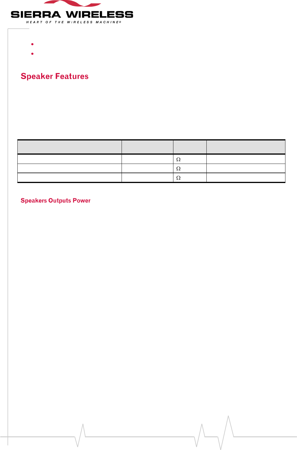
WM_DEV_Q26EX_PTS_002 Rev 006 Page 65 of 112
Product Technical Specification and
Customer Design Guidelines
C2: Must be tuned, as per the design.
L1: Must be tuned, as per the design.
The connection is single-ended on SPK1 and is differential or single-ended on SPK2. Using a
differential connection to reject common mode noise and TDMA noise is strongly recommended.
Moreover in single-ended mode, the power is divided by 4. When using a single-ended connection,
be sure to have a very good ground plane, a very good filtering as well as shielding in order to avoid
any disturbance on the audio path.
Table 38. Speaker information
Parameter
Typ
Unit
Connection
Z (SPK1P, SPK1N)
16 or 32
single-ended mode
Z (SPK2P, SPK2N)
4
single-ended mode
Z (SPK2P, SPK2N)
8
Differential mode
The both speakers maximum power output are not similar, that is due to the different configuration
between the Speaker1 which is only single ended and the speaker2 which can be differential, so
speaker2 can provides more power.
The maximal specifications given below are available with the maximum power output configuration
values set by an AT command. The typical values are recommended.
WM_DEV_Q26EX_PTS_002 Rev 006 Page 66 of 112
Product Technical Specification and
Customer Design Guidelines
With the SPK1 interface, only single ended speaker connection is allowed
Equivalent circuits of SPK1
Table 39. Electrical Characteristics of SPK1
Parameters
Min
Typ
Max
Unit
Biasing voltage
-
1.30
V
Output swing
voltage
RL=16 : AT+VGR=-1600**;
single-ended
-
1.7
-
Vpp
RL=32 ; AT+VGR=-1600**;
single-ended
-
1.9
2.75
Vpp
RL
Load resistance
14.5
32
-
IOUT
Output current;
single-ended; peak value
RL=16
-
40
85
mA
RL=32
-
22
-
mA
POUT
RL=16 ; AT+VGR*=-1600**
-
25
mW
RL=32 ; AT+VGR*=-1600**
-
16
27
mW
RPD
Output pull-down resistance at power-down
28
40
52
k
*The output voltage depends of the output speaker gain set by AT command. Please refer to the document AT command User
Guide [7].
** This value is given in dB, but it’s possible to toggle to index value. Please refer to the document :AT command User Guide [7]
Q26 Extreme
WM_DEV_Q26EX_PTS_002 Rev 006 Page 67 of 112
Product Technical Specification and
Customer Design Guidelines
The SPK2 interface allows differential and single ended speaker connection
Equivalent circuits of SPK2
Table 40. Electrical Characteristics of SPK2
Parameters
Min
Typ
Max
Unit
Biasing voltage
SPK2P and SPK2N
1.30
V
Output swing
voltage
RL=8 : AT+VGR=-1000*; single ended
-
-
2
Vpp
RL=8 : AT+VGR=-1000*; differential
-
-
4
Vpp
RL=32 : AT+VGR=-1000*; single ended
-
-
2.5
Vpp
RL=32 : AT+VGR=-1000*; differential
-
-
5
Vpp
RL
Load resistance
6
8
-
IOUT
Output current; peak value; RL=8
-
-
180
mA
POUT
RL=8 ; AT+VGR=-1000*;
-
-
250
mW
RPD
Output pull-down resistance at power-down
28
40
52
k
VPD
Output DC voltage at power-down
-
-
100
mV
*The output voltage depends of the output speaker gain set by AT command. Please refer to the document: AT command User
Guide [7].This value is given in dB, but it’s possible to toggle to index value.
If a singled ended solution is used with the speaker2 output, only one of the both SPK2 has to be
chosen. The result is a maximal output power divided by 4.
Q26 Extreme
WM_DEV_Q26EX_PTS_002 Rev 006 Page 68 of 112
Product Technical Specification and
Customer Design Guidelines
SPKxP
SPKxN
Figure 27. Example of Speaker differential connection
Impedance of the speaker amplifier output in differential mode is:
R 1 ohm +/-10 %.
The connection between the Wireless CPU pins and the speaker must be designed in order to keep the
serial impedance lower than 3 ohms in differential mode.
Typical implementation:
SPKxP
C1
+
SPKxN
C2
+
Zhp
Speaker
C3
33 pF
to
100 pF
R1
Figure 28. Example of Speaker single-ended connection
6.8µF < C1 < 47µF (depends on speaker characteristics and output power).
C1 = C2.
R1 = Zhp.
Use of a single-ended connection results in output power loss (- 6 dB) when compared to a
differential connection.
Nevertheless, in a 32 ohms speaker case, you should use a cheaper and smaller solution:
R1 = 82 ohms and C2 = 6.8µF (ceramic).
The connection between the Wireless CPU pins and the speaker must be designed in order to keep the
serial impedance lower than 1.5 ohm in differential mode.
When SPK1 channel is used, only SPK1P is useful, SPK1N may be left open.
WM_DEV_Q26EX_PTS_002 Rev 006 Page 69 of 112
Product Technical Specification and
Customer Design Guidelines
Type: 10 mW, electro-magnetic.
Impedance:
Z = 8 ohm for hands-free (SPK2),
Z = 32 ohm for headset kit (SPK1).
Sensitivity: 110 dB SPL minimum (0 dB = 20 µPa).
Frequency response compatible with the GSM specifications.
Table 41. Pin definitions
Signal
Pin
number
I/O
I/O type
Description
MIC1P
40
I
Analog
Microphone 1 positive input
MIC1N
38
I
Analog
Microphone 1 negative input
MIC2P
36
I
Analog
Microphone 2 positive input
MIC2N
34
I
Analog
Microphone 2 negative input
SPK1P
35
O
Analog
Speaker 1 positive output
SPK1N
37
O
Analog
Speaker 1 negative output
SPK2P
39
O
Analog
Speaker 2 positive output
SPK2N
41
O
Analog
Speaker 2 negative output
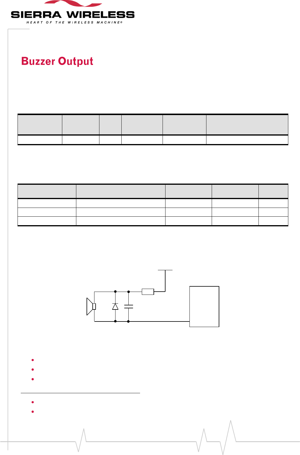
WM_DEV_Q26EX_PTS_002 Rev 006 Page 70 of 112
Product Technical Specification and
Customer Design Guidelines
This output is controlled by a pulse width modulation controller and may be used only as buzzer.
BUZZER0 is an open drain output. A buzzer can be directly connected between this output and
VBATT. The maximum current is 100 mA (PEAK).
Table 42. Pin description of PWM/Buzzer output
Signal
Pin
number
I/O
I/O type
Reset state
Description
BUZZER0
15
O
Open drain
Z
Buzzer output
See Chapter 3.3, “Electrical information for digital I/O” for Open drain, 2V8 and 1V8 voltage characteristics and Reset state
definition.
Table 43. Electrical characteristics
Parameter
Condition
Minimum
Maximum
Unit
VOL on
Iol = 100mA
0.4
V
IPEAK
VBATT = VBATTmax
100
mA
Frequency
1
50000
Hz
The maximum peak current is 80 mA and the maximum average current is 40 mA. A diode against
transient peak voltage must be added as described below.
BUZZ-OUT
C1
D1
VBATT
R1 Q26
Extreme
Wireless
CPU
15
Figure 29. Example of buzzer implementation
Where:
R1 must be selected in order to limit the current at IPEAK max
C1 = 0 to 100 nF (depends on the buzzer type)
D1 = BAS16 (for example)
Recommended characteristics for the buzzer:
Electro-magnetic type
Impedance: 7 to 30 ohms
WM_DEV_Q26EX_PTS_002 Rev 006 Page 71 of 112
Product Technical Specification and
Customer Design Guidelines
Sensitivity: 90 dB SPL min @ 10 cm
Current: 60 to 90 mA
BUZZ-OUT output may also be used to drive a LED as shown in the Figure 33.
BUZZ-OUT
(pin 15)
VBATT
« BUZZER »
D1
1
2
R1
470
Figure 30. Example of LED driven by the BUZZ-OUT output
R1 value depends on the LED (D1) characteristics.
The Q26 Extreme Wireless CPU® supports one battery charging circuit, two algorithms and one
hardware charging mode (pre-charging) for 3 battery technologies:
Ni-Cd (Nickel-Cadmium) with algorithm 0
Ni-Mh (Nickel-Metal Hydride) with algorithm 0
Li-Ion (Lithium-Ion) with the embedded PCM (Protection Circuit Module).algorithm 1
The two algorithms control a switch, which connects the CHG-IN signal to the VBATT signal. The
algorithm controls the frequency and the connected time of the switching. During the charging
procedure, battery charging level is monitored and when Li-Ion algorithm is used, battery
temperature is monitored via the ADC1/BAT-TEMP input.
One more charging procedure is provided by the Q26 Extreme Wireless CPU®. This is called “Pre-
charging” mode, but is a special charging mode because it is activated only when the Wireless CPU®
is OFF. Control is in this case only performed by the hardware. The purpose of this charging mode is
to avoid battery damage by preventing the battery from being discharged to below the minimum
battery level.
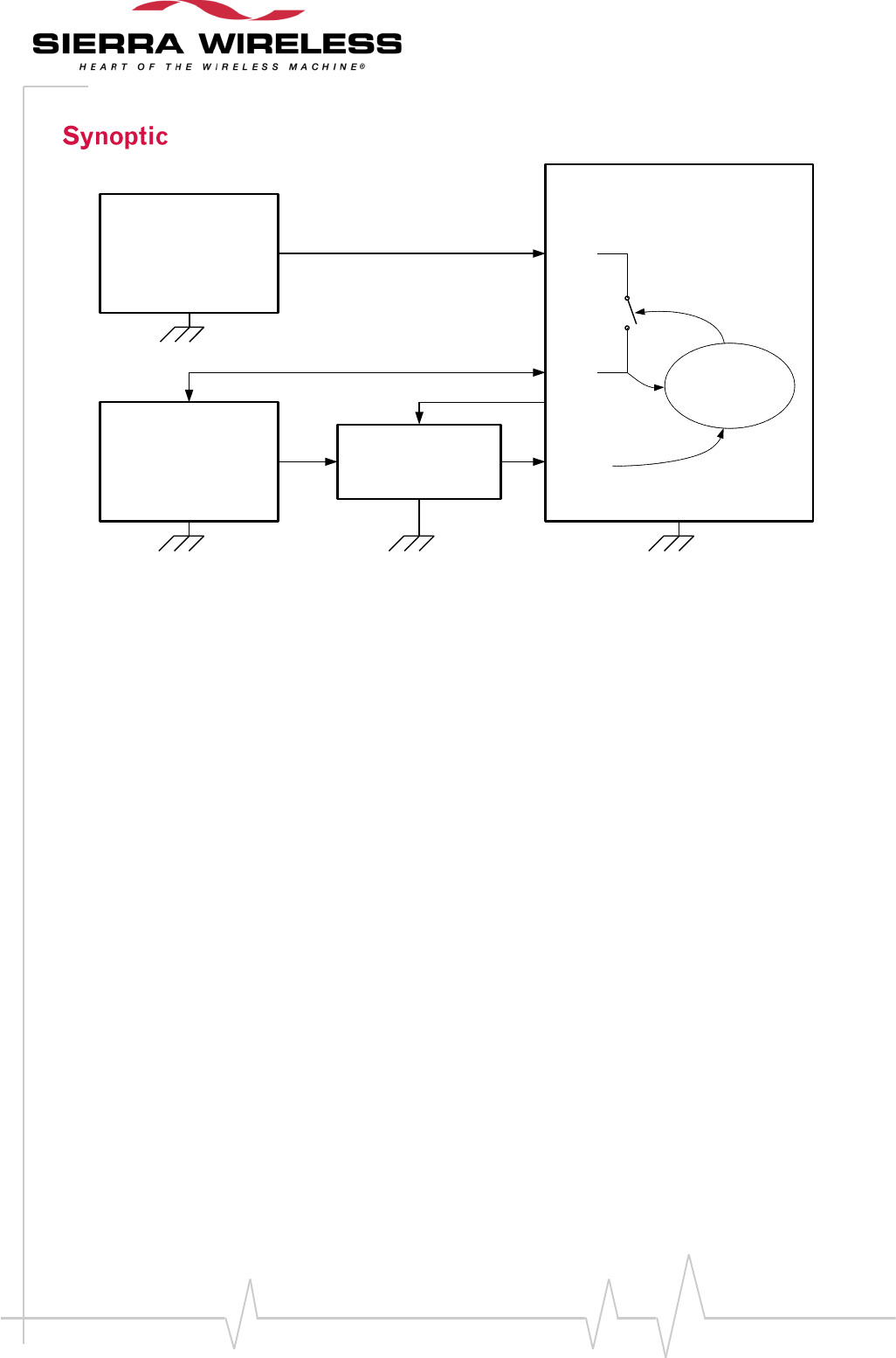
WM_DEV_Q26EX_PTS_002 Rev 006 Page 72 of 112
Product Technical Specification and
Customer Design Guidelines
CHARGER
DC output
Q26 Extreme
Wireless CPU
BATTERY TEMPERATURE
SENSOR
INTERFACE
CHG-IN
VCC_2V8
NTC BAT-TEMP
VBATT ALGORITHM
CONTROL
Figure 31. Synoptic of battery charging
Q26 Extreme Wireless CPU® charging circuit is composed of a transistor switch (between CHG-IN
pin6, 8 and VBATT pin 1, 2, 3, 4). Charging is controlled by 2 software’s algorithms.
A dedicated ADC input BAT-TEMP (pin 20) for temperature monitoring (only for Li-Ion battery
technology).
WM_DEV_Q26EX_PTS_002 Rev 006 Page 73 of 112
Product Technical Specification and
Customer Design Guidelines
To use the charging functionality, 3 hardware items are required:
Charger power supply
It provides a DC current power supply limited to 800mA and with voltage range,
according to the battery choice and to the Q26 Extreme Wireless CPU® specification.
Battery
The charging functionality must be used with rechargeable battery only. Three battery
types are supported: Li-Ion, Ni-Mh and Ni-Cd.
If the Q26 Extreme Wireless CPU® is not powered (VBATT pin 1,2,3,4) by a rechargeable
battery, it is mandatory to left open the CHG-IN input (pin 6,8).
Analog temperature sensor
Analog temperature sensor is only used for Li-Ion batteries to monitor the battery
temperature. This sensor is composed of NTC sensor and several resistors.
The following table defines and specifies the AC/DC adapter for a battery cell.
Table 44. Charger recommendations
Parameter
Min
Typ
Max
Unit
Remark
Input voltage
90
265
Vac
Input frequency
45
65
Hz
Output voltage limit
6
V
No load
Output voltage limit
4.6
V
Io max
Output current
(1)
1C(2)
(3)
mA
Output Voltage
Ripple
150
mVpp
Io max
Vout=5.3V
Note: See the cell battery specifications for conditions of current charging.
Note: 1C = Nominal capacity (of the battery cell).
Note: See the cell battery specifications for conditions of current charging.
We recommend, the output voltage (Vo) falls under 1.18V in less than 1 second, when the adapter
AC/DC is unplugged.
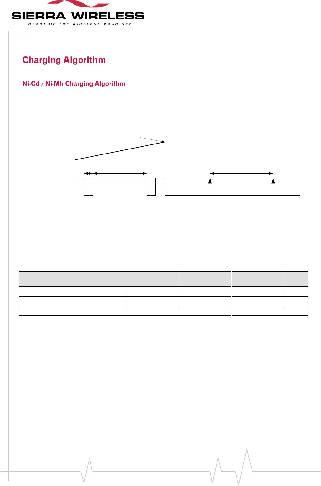
WM_DEV_Q26EX_PTS_002 Rev 006 Page 74 of 112
Product Technical Specification and
Customer Design Guidelines
To charge the battery, the algorithm measures battery level when the switch is open (time T2) and
charges the battery by closing the switch (time T3). When the battery is charged (battery voltage has
reached BattLevelMax) the switch is open for time T3.
BattLevelMax
T1T2 T3
Battery Level
Switch State
opened
closed
T1 : Charging pulse duration 1sec
T2 : TPulseINCharge Time between charging pulses
T3 : TPulseOutCharge Time between Battery Monitoring events (Battery charged)
Figure 32. Ni-Cd / Ni-Mh charging waveform
Table 45. Electrical characteristics of Ni-Cd / Ni-Mh battery timing charge
Parameter
Min
Typ
Max
Unit
T1
1
s
T2
0.1
s
T3
5
s
Note: T1,T2,T3 and BattLevelMax may be configured by AT command.
The battery level is monitored by the software (but not temperature).
The Li-Ion algorithm provides battery temperature monitoring, which is highly recommended to
prevent battery damage during the charging phase.
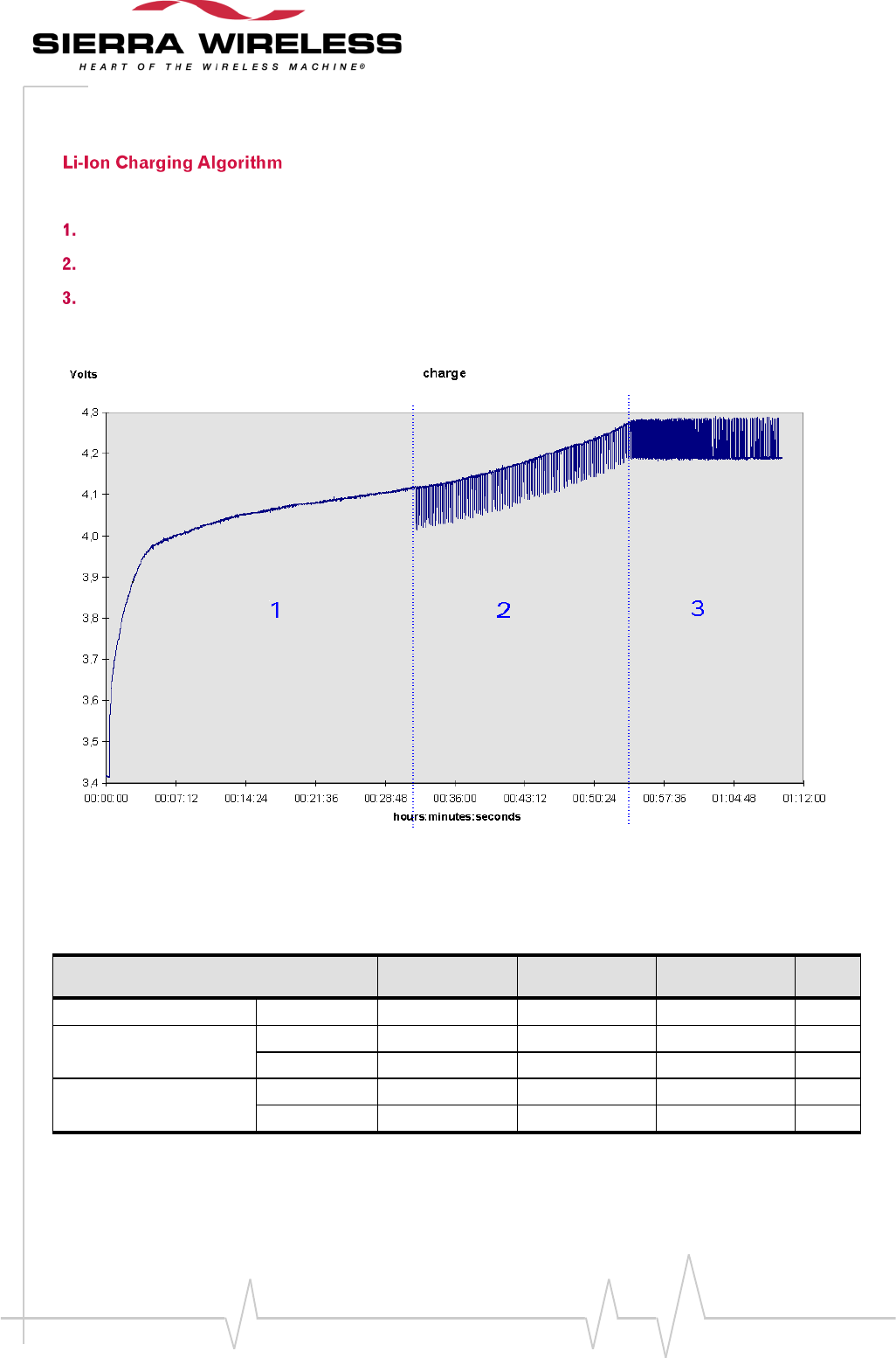
WM_DEV_Q26EX_PTS_002 Rev 006 Page 75 of 112
Product Technical Specification and
Customer Design Guidelines
The Li-Ion charger algorithm can be broken down into three phases:
Constant charge
Beginning of pulse charge
End of pulse charge
The three phases can be seen on the following waveform for full charging:
Figure 33. Li-Ion full charging waveform
Table 46. Electrical characteristics of Li-Ion battery timing charge
Parameter
Min
Typ
Max
Unit
Step 1 switching
Closed
Always
s
Step 2 switching
Open
0.1
s
Closed
1
s
Step 3 switching
Open
0.1
3
s
Closed
1
s
WM_DEV_Q26EX_PTS_002 Rev 006 Page 76 of 112
Product Technical Specification and
Customer Design Guidelines
When a charger DC power supply is connected to the CHG-IN input and if the voltage battery is
between 2.8V* and 3.2V, a constant current of 50mA is provided to the battery.
When the battery is able to supply the Q26 Extreme Wireless CPU®, it is automatically powered on
and the software algorithm is activated to finish the charge.
* For the Lithium-ion battery, the minimum voltage must be higher than PCM lock level.
Note: When pre-charging is launched, the LED0 output blinks automatically.
Warning: The Q26 Extreme Wireless CPU® can not release the PCM
protection inside Lithium battery pack. Voltage forbidden on the
CHG-IN signal if no battery connected on VBATT signals.
Temperature monitoring is only available for the Li-Ion battery with algorithm 1. The ADC1/BAT-
TEMP (pin 20) input must be used to sample the temperature analog signal provided by an NTC
temperature sensor. The minimum and maximum temperature range may be set by AT command.
Table 47. Pin description of battery charging interface
Signal
Pin number
I/O
I/O type
Description
CHG-IN
6,8
I
Analog
Current source input
BAT-TEMP
20
I
Analog
A/D converter
Table 48. Electrical characteristics of battery charging interface
Parameter
Minimum
Typ
Maximum
Unit
Charging operating temperature
0
50
°C
ADC1/BAT-TEMP
(pin 20 )
Maximum output code
1635
LSB
Sampling rate
216
S/s
Input Impedance ( R )
1
M
Input signal range
0
2
V
CHG-IN (pin 6, 8 )
Voltage (for I=Imax)
4.8*
V
Voltage (for I=0)
6*
V
DC Current
400**
800
mA
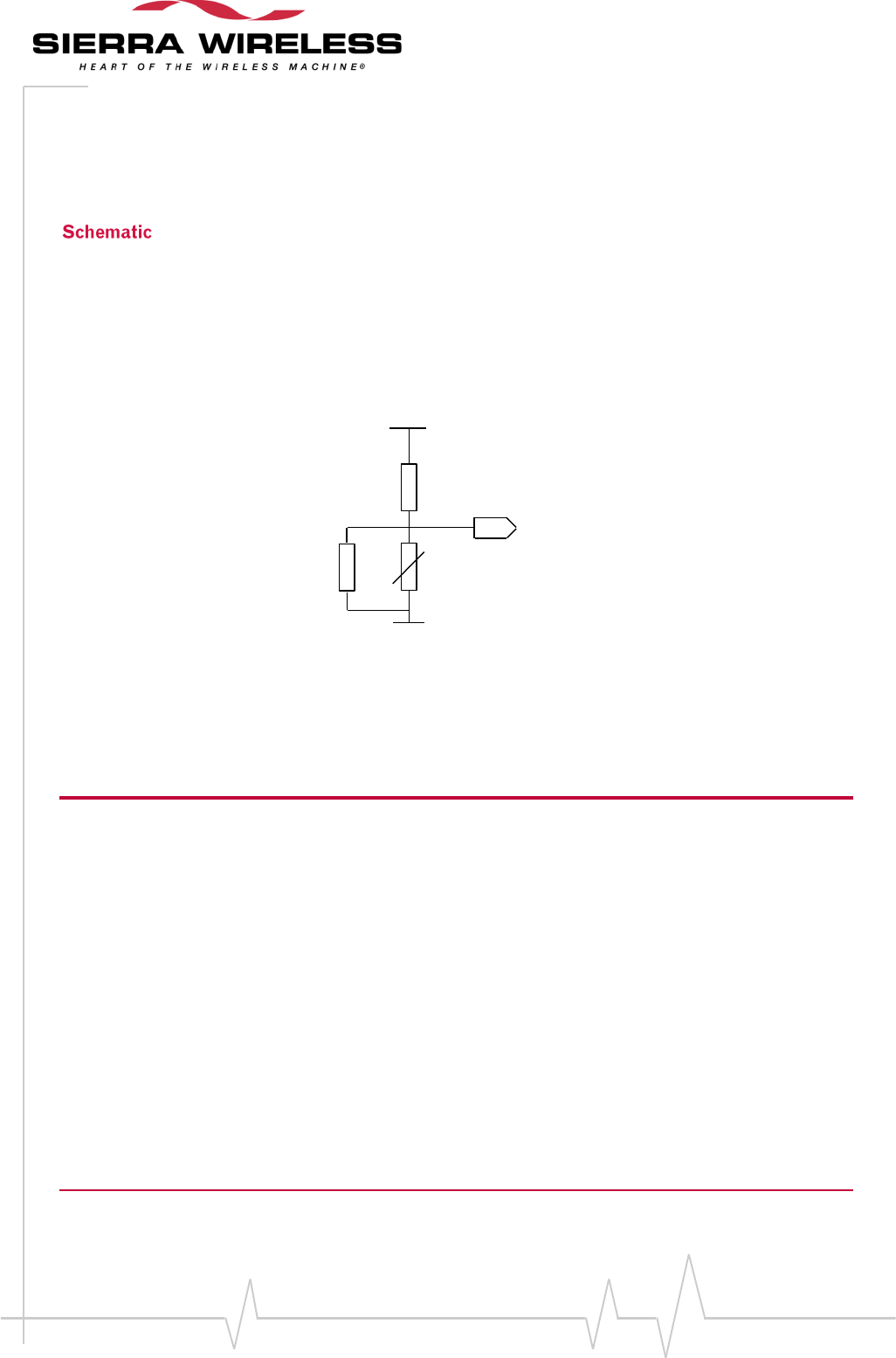
WM_DEV_Q26EX_PTS_002 Rev 006 Page 77 of 112
Product Technical Specification and
Customer Design Guidelines
* To be configured as specified by the battery manufacturer
** : Take care ; this value has to be selected in function of the power consumption mode used: please refer to the power
consumption tables § 3.2.2.
The VCC_2V8 (pin 10) voltage provided by the Q26 Extreme Wireless CPU® may be used to polarize
the NTC. However, the additional resistors R1 and R2, must be used to adjust the maximum voltage
of the ADC input to 2volts.
If any other polarized voltage is used, the resistors must be adapted.
It is not recommended to used the VCC_1V8 (pin 5) voltage.
GND
VCC_2V8
BAT-TEMP
(pin 20)
R1
R2
R(t) NTC
Figure 34. Example of ADC application
The R(t) resistor is the NTC and must be close to the battery., it is usually integrated into the battery.
Warning: The Charger DC power supply must have an output current limited
to 800mA.
The maximum Charger output current, provided to the battery, must
be accorded to the battery electrical characteristics.
Li-Ion batteries must be used with the embedded PCM (Protection
Circuit Module).
The maximum charging voltage is up to 4,3V (Software drive)
At the first plug, if the batter Li-ion is locked by its PCM, the charger
function does not work.
At the first plug, if the battery Li-ion is locked by its PCM the charger
function doesn't work.
WM_DEV_Q26EX_PTS_002 Rev 006 Page 78 of 112
Product Technical Specification and
Customer Design Guidelines
This input is used to switch the Q26 Extreme Wireless CPU® ON or OFF.
A high-level signal must be provided on the ON/~OFF pin to switch ON the Wireless CPU®. The
voltage of this signal has to be maintained higher than 0.8 x VBATT during a minimum of 1500ms.
This signal can be left at high level until switch-off.
To switch OFF the Wireless CPU®, the ON/OFF pin must be released. The Wireless CPU® can be
switched off via the Operating System.
Table 49. Pin description
Signal
Pin number
I/O
I/O type
Description
ON/ OFF
19
I
CMOS
Wireless CPU® Power-ON
Table 50. Electrical characteristics of the signals
Parameter
I/O type
Minimum
Maximum
Unit
VIL
CMOS
VBATT x 0.2
V
VIH
CMOS
VBATT x 0.8
VBATT
V
Warning: All external signals must be inactive when the Wireless CPU®
module is OFF to avoid any damage when starting and allow the
Wireless CPU® to start and stop correctly.
Once the Wireless CPU® is supplied, the application must set the ON/OFF signal to high to start the
Wireless CPU® power-ON sequence. The ON/OFF signal must be held high during a minimum delay
of Ton/off-hold (Minimum hold delay on the ON/~OFF signal) to power-ON. After this delay, an internal
mechanism maintains the Wireless CPU® in power-ON condition.
During the power-ON sequence, an internal reset is automatically performed by the Wireless CPU®
for 40ms (typical). Any external reset should be avoided during this phase.
Once initialization is completed (timing is USIM- and network-dependent), the AT interface answers
"OK" to the application. For further details, please check the AT Commands Manual [5].
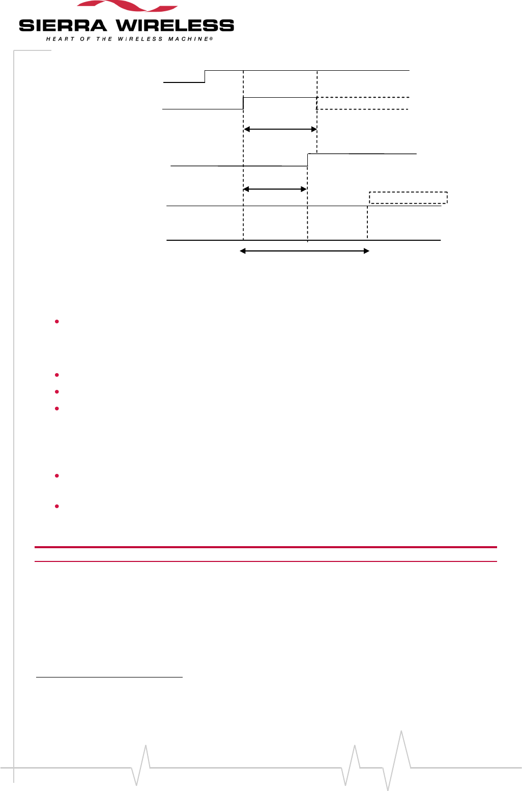
WM_DEV_Q26EX_PTS_002 Rev 006 Page 79 of 112
Product Technical Specification and
Customer Design Guidelines
POWER SUPPLY
ON/OFF
STATE OF THE
Wireless CPU ®
Wireless CPU ®
OFF
IBB+RF < 22µA
AT answers « OK »
Wireless CPU ®
READY
Ton/off-hold
(2000ms min)
SIM and Network dependent
RESET mode
IBB+RF=20 to 40mA
INTERNAL RST
Trst
(40ms typ)
Wireless CPU ®
ON
IBB+RF<120mA
(no loc. update)
Figure 35. Power-ON sequence (no PIN code activated)
The duration of the firmware power-up sequence depends on:
the need to perform a recovery sequence if the power has been lost during a flash memory
modification.
Other factors have a minor influence
the number of parameters stored in EEPROM by the AT commands received so far
the ageing of the hardware components, especially the flash memory
the temperature conditions
The recommended way to de-assert the ON/~OFF signal is to use either an AT command or WIND
indicators: the application must detect the end of the power-up initialization and de-assert ON/~OFF
afterwards.
Send an “AT” command and wait for the “OK” answer: once the initialization is complete the
AT interface answers « OK » to “AT” message1.
Wait for the “+WIND: 3” message: after initialization, the Wireless CPU®, if configured to do
so, will return an unsolicited “+WIND: 3” message. The generation of this message is enabled
or disabled via an AT command.
Note: See also “AT Commands Manual” [5] for more information on these commands.
Proceeding thus – by software detection - will always prevent the application from de-asserting the
ON/~OFF signal too early.
If WIND indicators are disabled or AT commands unavailable or not used, it is still possible to de-
assert ON/~OFF after a delay long enough (Ton/off-hold) to ensure that the firmware has already
completed its power-up initialization.
1 If the application manages hardware flow control, the AT command can be sent during the initialisation phase.
WM_DEV_Q26EX_PTS_002 Rev 006 Page 80 of 112
Product Technical Specification and
Customer Design Guidelines
The table below gives the minimum values of Ton/off-hold:
Table 51. Ton/off-hold minimum values
Open AT® Firmware
Ton/off-hold
Safe evaluations of the firmware power-up time
Open AT® Software Suite v2.30
8 s (TBC)
The above figure take the worst cases into account: power-loss recovery operations, slow flash memory operations in high
temperature conditions, and so on. But, they are safe because they are large enough to ensure that ON/~OFF is not de-
asserted too early.
Typical power-up initialization time figures for best cases conditions (no power-loss recovery,
fast and new flash memory…) approximate 3.5 seconds in every firmware version. But
releasing ON/~OFF after this delay does not guarantee that the application will actually start-
up if for example the power plug has been pulled off during a flash memory operation, like a
phone book entry update or an AT&W command…
The ON/~OFF signal can be left at a high level until switch OFF. But this is not recommended
as it will prevent the AT+CPOF command from performing a clean power-off. (see also Note
in section 0 on Power-OFF for an alternate usage)
When using a battery as power source, it is not recommended to let this signal high:
If the battery voltage is too low and the ON/~OFF signal at low level, an internal mechanism
switches OFF the Wireless CPU®. This automatic process prevents the battery to be over
discharged and optimize its life span.
During the power-ON sequence, an internal reset is automatically performed by the Wireless
CPU® for 40 ms (typical). Any external reset should be avoided during this phase.
After a reset (hardware or software), if the ON/~OFF signal is OFF (Low level) the Wireless
CPU® switches OFF.
To power-OFF the Wireless CPU® correctly, the application must reset the ON/OFF signal and then
send the AT+CPOF command to deregister from the network and switch off the Wireless CPU®.
Once the "OK" response is issued by the Wireless CPU®, the power supply can be switched off.
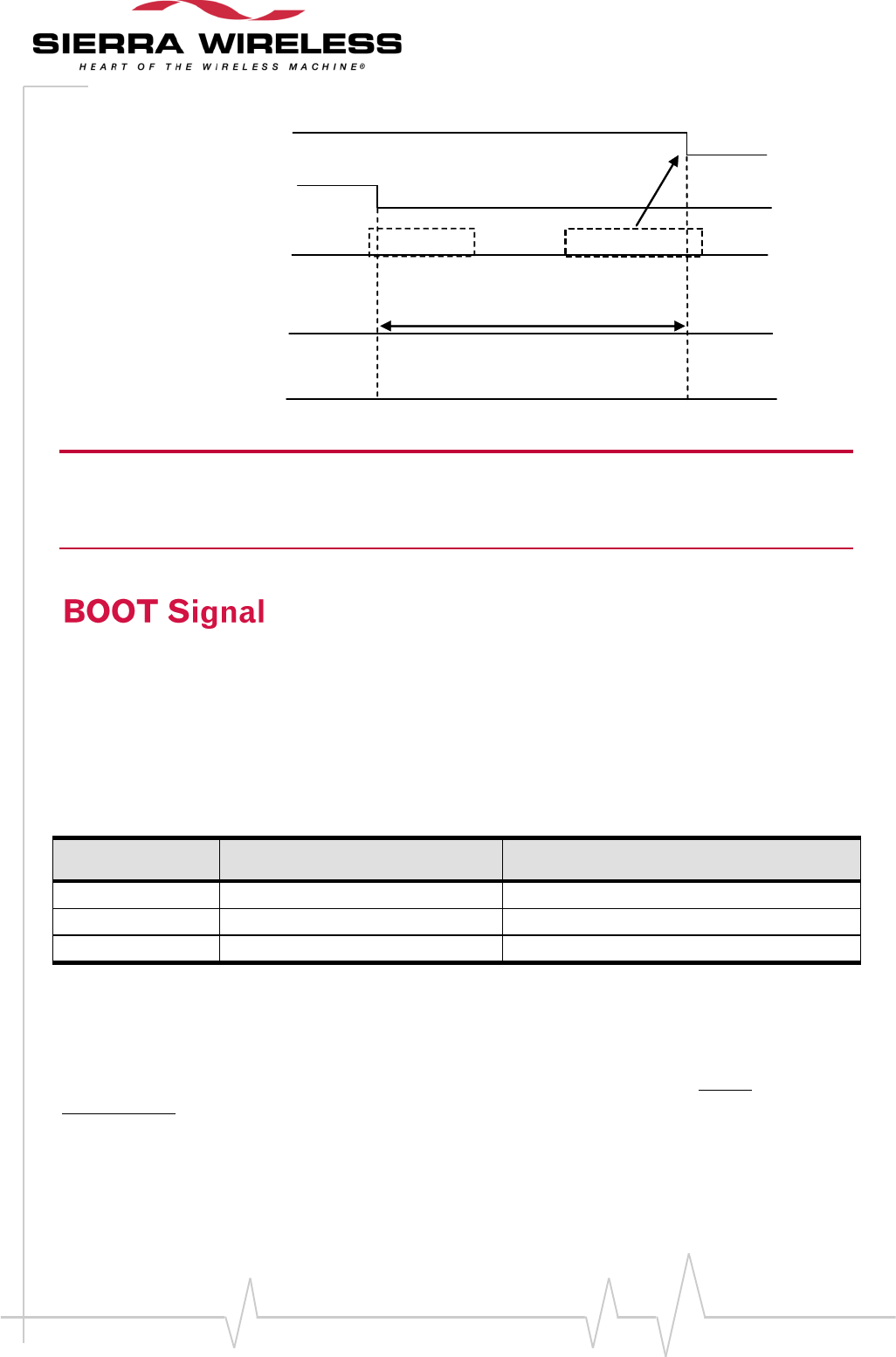
WM_DEV_Q26EX_PTS_002 Rev 006 Page 81 of 112
Product Technical Specification and
Customer Design Guidelines
POWER SUPPLY
ON/OFF
AT COMMAND
STATE OF THE
Wireless CPU®
AT+CPOF
Wireless CPU®
READY
Wireless CPU®
OFF
IBB+RF<22µA
Network dependent
OK response
Figure 36. Power-OFF sequence
Note: If the ON/~OFF pin is maintained to ON (High Level), then the Wireless CPU® can’t be switched OFF.
Connecting a charger on the Wireless CPU® as exactly the same effect than setting the ON/~OFF
signal. In particular the Wireless CPU® will not POWER-OFF after the AT+CPOF command, unless the
Charger is disconnected.
A specific BOOT control pin is available to download the Q26 Extreme Wireless CPU® only if the
standard XModem download, controlled with AT command, is not possible).
A specific PC software program, provided by Wavecom, is needed to perform this specific download.
The BOOT pin must be connected to VCC_1V8 for this specific download.
Table 52. Operating mode description
BOOT
Operating mode
Comment
Leave open
Normal use
No download
Leave open
Download XModem
AT command for Download AT+WDWL
1
Download specific
Need Wavecom PC software
For more information, see Q26 Extreme Wireless CPU® / Open AT® Software Suite AT Command User Guide [5].
This BOOT pin must be left open either for normal use or XModem download.
However, in order to render the development and maintenance phases easier, it is highly
recommended to set a test point, either a jumper or a switch on the VCC_1V8 (pin 5) power supply.
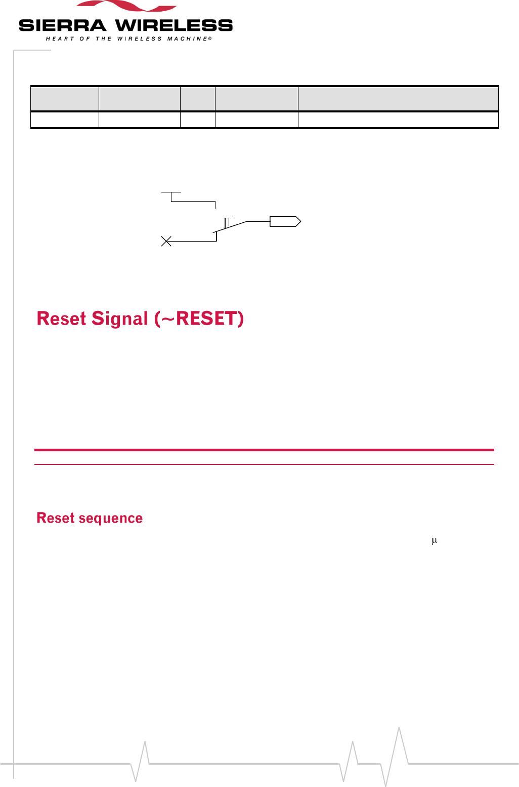
WM_DEV_Q26EX_PTS_002 Rev 006 Page 82 of 112
Product Technical Specification and
Customer Design Guidelines
Table 53. Pin description
Signal
Pin number
I/O
I/O type
Description
BOOT
16
I
1V8
Download mode selection
1
2
3
Switch
BOOT (pin 16)
VCC_1V8
(pin 5)
Figure 37. Example of BOOT pin implementation
This signal is used to force a reset procedure by providing low level for at least 200µs. This signal
must be considered as an emergency reset only. A reset procedure is already driven by the internal
hardware during the power-up sequence.
This signal may also be used to provide a reset to an external device (at power-up only). If no external
reset is necessary, this input may be left open. If used (emergency reset), it must be driven by an open
collector or an open drain.
The Wireless CPU® remains in reset mode as long as the ~RESET signal is held low.
Caution: This signal should only be used for “emergency” resets.
An Operating System reset is to be preferred to a hardware reset.
To activate the "emergency" reset sequence, the ~RESET signal must be set to low for 200 s minimum.
As soon as the reset is completed, the AT interface answers "OK" to the application.
WM_DEV_Q26EX_PTS_002 Rev 006 Page 83 of 112
Product Technical Specification and
Customer Design Guidelines
RESET mode
IBB+RF=20 to 40mA
~RESET
STATE OF THE
Wireless CPU®
Wireless
CPU®
READY
Rt = Min1:200 s
or Typ2 = 40ms
AT answers “OK”
Wireless CPU®
READY
SIM and network
dependent
Wireless CPU®
ON
IBB+RF<120mA without
loc update
Ct = Typ:34ms
Figure 38. Reset sequence waveform
At power-up, the ~RESET time (Rt) is carried out after switching ON the Wireless CPU®. It is
generated by the internal Q26 Extreme Wireless CPU® voltage supervisor.
The ~RESET time is provided by the internal RC component. To keep the same time, it is not
recommended to connect another R or C component on the ~RESET signal. Only a switch or an open
drain gate is recommended.
Ct is the cancellation time required for the Q26 Extreme Wireless CPU® initialization. Ct is
automatically carried out by the Q26 Extreme Wireless CPU® after a hardware reset.
Table 54. Electrical characteristics of the signals
Parameter
Minimum
Typ
Maximum
Unit
Input Impedance ( R )*
100
k
Input Impedance ( C )
10
nF
~RESET time (Rt) 1
200
µs
~RESET time (Rt) 2 at power up only
20
40
100
ms
Cancellation time (Ct)
34
ms
VH
0.57
V
VIL
0
0.57
V
VIH
1.33
V
* internal pull-up VH: Hysterisis Voltage
1 This reset time is the minimum to be carried out on the ~RESET signal when the power supply is already stabilized.
2 This reset time is internally carried out by the Wireless CPU® power supply supervisor only when the Wireless CPU®
power supplies are powered ON.
Table 55. Pin description
Signal
Pin number
I/O
I/O type
Description
~RESET
18
I/O Open Drain
1V8
Wireless CPU® Reset
WM_DEV_Q26EX_PTS_002 Rev 006 Page 84 of 112
Product Technical Specification and
Customer Design Guidelines
GND
1
2
3
Switch
RESET (pin 18)
Figure 39. Example of ~RESET pin connection with switch configuration
GND
RESET (pin 18)
Reset
command T1
Rohm DTC144EE
Figure 40. Example of ~RESET pin connection with transistor configuration
Open collector or open drain transistor may be used. If an open collector is selected, T1 may be a
Rohm DTC144EE.
Table 56. Reset command
Reset command
~RESET (pin 18)
Operating mode
1
0
Reset activated
0
1
Reset inactive
The Q26 Extreme Wireless CPU® provides three external interrupt inputs. These interrupt inputs can
be activated on:
High to low edge
Low to high edge
Low to high and high to low edge
When used, the interrupt inputs must not be left open.
If not used, they must be configured as GPIOs.
Table 57. Pin description
Signal
Pin
number
I/O
I/O type
Reset
state
Description
Multiplexed
with
INT2
51
I
1V8
Pull-up
External Interrupt 2
~CS2 / GPIO1
INT1
49
I
2V8
Z
External Interrupt 1
GPIO25
INT0
50
I
1V8
Z
External Interrupt 0
GPIO3
WM_DEV_Q26EX_PTS_002 Rev 006 Page 85 of 112
Product Technical Specification and
Customer Design Guidelines
See Chapter Caution:, “Electrical information for digital I/O” for Open drain, 2V8 and 1V8 voltage characteristics and Reset
state definition.
Table 58. Electrical characteristics of the signals
Parameter
Minimum
Maximum
Unit
INT1
VIL
0.84
V
VIH
1.96
V
INT0 , INT2
VIL
0.54
V
VIH
1.33
V
These outputs may be used to power some external functions and only available when the Wireless
CPU is ON.
Table 59. Pin description
Signal
Pin number
I/O
I/O type
Description
VCC_2V8
10
O
Supply
Digital supply
VCC_1V8
5
O
Supply
Digital supply
Table 60. Electrical characteristics of the signals
Parameter
Minimum
Typ
Maximum
Unit
VCC_2V8
Output voltage
2.74
2.8
2.86
V
Output Current
15
mA
VCC_1V8
Output voltage
1.76
1.8
1.94
V
Output Current
15
mA
These digital power supplies are mainly used to:
Pull-up signals such as I/O
Supply the digital transistors driving the LEDs
Supply the SIMPRES signal
Act as a voltage reference for ADC interface AUX-ADC (only for VCC_2V8)
The maximum current to be provided by each output is 15 mA.
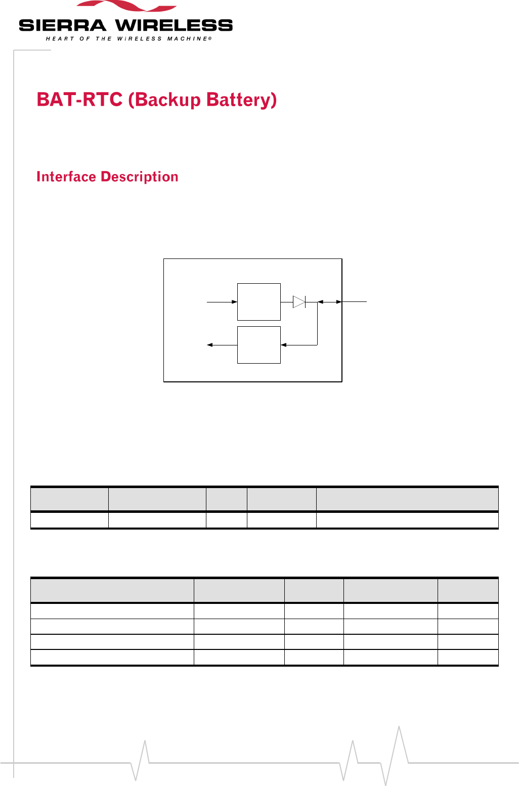
WM_DEV_Q26EX_PTS_002 Rev 006 Page 86 of 112
Product Technical Specification and
Customer Design Guidelines
The Q26 Extreme Wireless CPU® provides an input/output to connect a Real Time Clock (RTC) power
supply.
This pin is used as a back-up power supply for the internal Real Time Clock. The RTC is supported
by the Wireless CPU® when VBATT is available, but a back-up power supply is needed to save date
and time when VBATT is switched off (VBATT = 0V).
2.5V
regulator
1.8V
regulator
from VBATT
to RTC
Q26
Extreme
BAT-RTC (Pin 7)
Figure 41. Real Time Clock power supply
If the RTC is not used, this pin can be left open.
If VBATT is available, the back-up battery can be charged by the internal 2.5V power supply
regulator.
Table 61. Pin description
Signal
Pin number
I/O
I/O type
Description
BAT-RTC
7
I/O
Supply
RTC Back-up supply
Table 62. Electrical characteristics of the signals
Parameter
Minimum
Typ
Maximum
Unit
Input voltage
1.85
3.0
V
Input current consumption*
3.3
µA
Output voltage
2.45
V
Output current
2
mA
*Provided by an RTC back-up battery when Wireless CPU® power supply is off (VBATT = 0V).
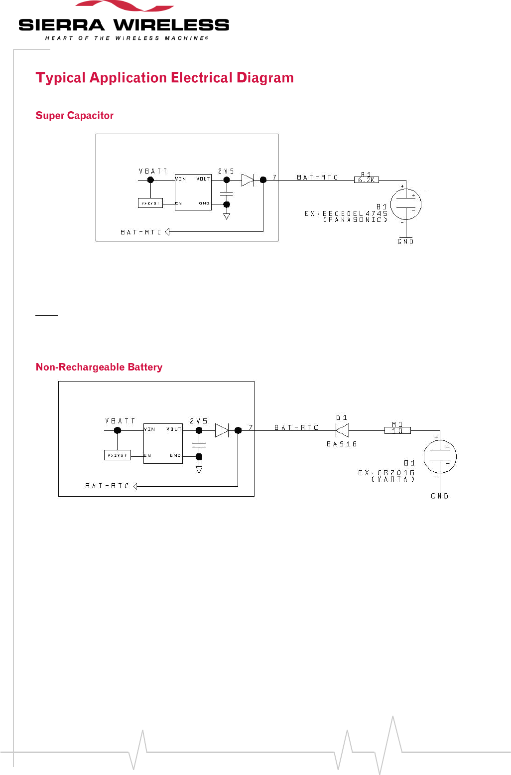
WM_DEV_Q26EX_PTS_002 Rev 006 Page 87 of 112
Product Technical Specification and
Customer Design Guidelines
Figure 42. RTC supplied by a gold capacitor
Estimated range with 0.47 Farad Gold Cap: 4 hours minimum.
Note:
The Gold Capacitor maximum voltage is 2.5 V.
Figure 43. RTC supplied by a non-rechargeable battery
The diode D1 is mandatory, in order to protect the non-rechargeable battery.
Estimated range with 85 mAh battery: 800 h minimum.
Q26 Extreme
Q26 Extreme
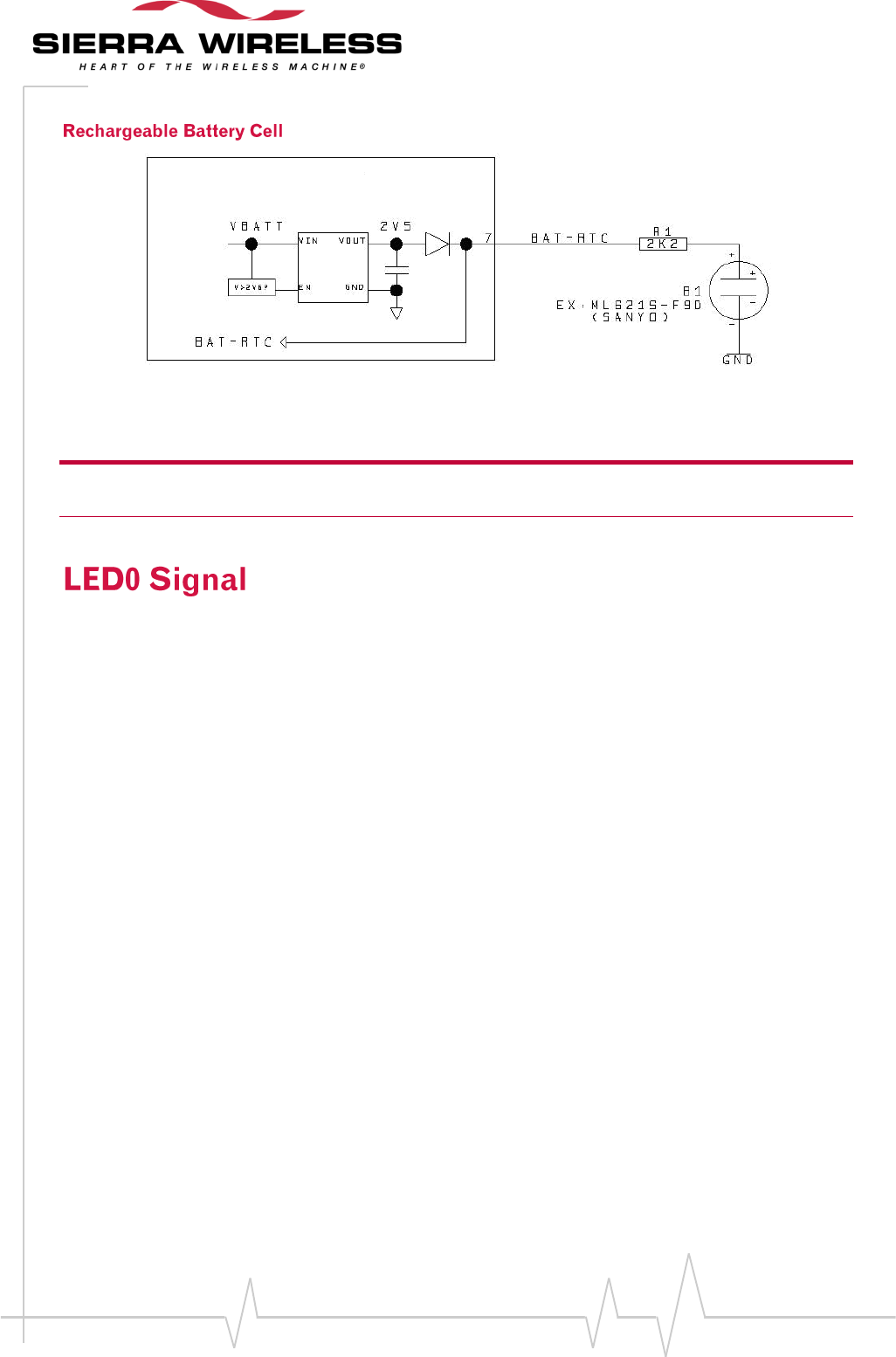
WM_DEV_Q26EX_PTS_002 Rev 006 Page 88 of 112
Product Technical Specification and
Customer Design Guidelines
Figure 44. RTC supplied by a rechargeable battery cell
Estimated range with 2 mAh rechargeable battery: ~15 hours.
Warning: Before battery cell assembly ensures that cell voltage is lower than
2.75 V to avoid any damage to the Wireless CPU.
LED0 is an open drain output. A LED and a resistor can be directly connected between this output
and VBATT.
When the Q26 Extreme Wireless CPU® is OFF, if 2.8V < VBATT < 3.2V and a charger is connected on
CHG-IN inputs, this output flashes ( 100 ms ON, 900 ms OFF ) to indicate the pre-charging phase of
the battery.
When the Q26 Extreme Wireless CPU® is ON, this output is used to indicate network status.
Q26 Extreme
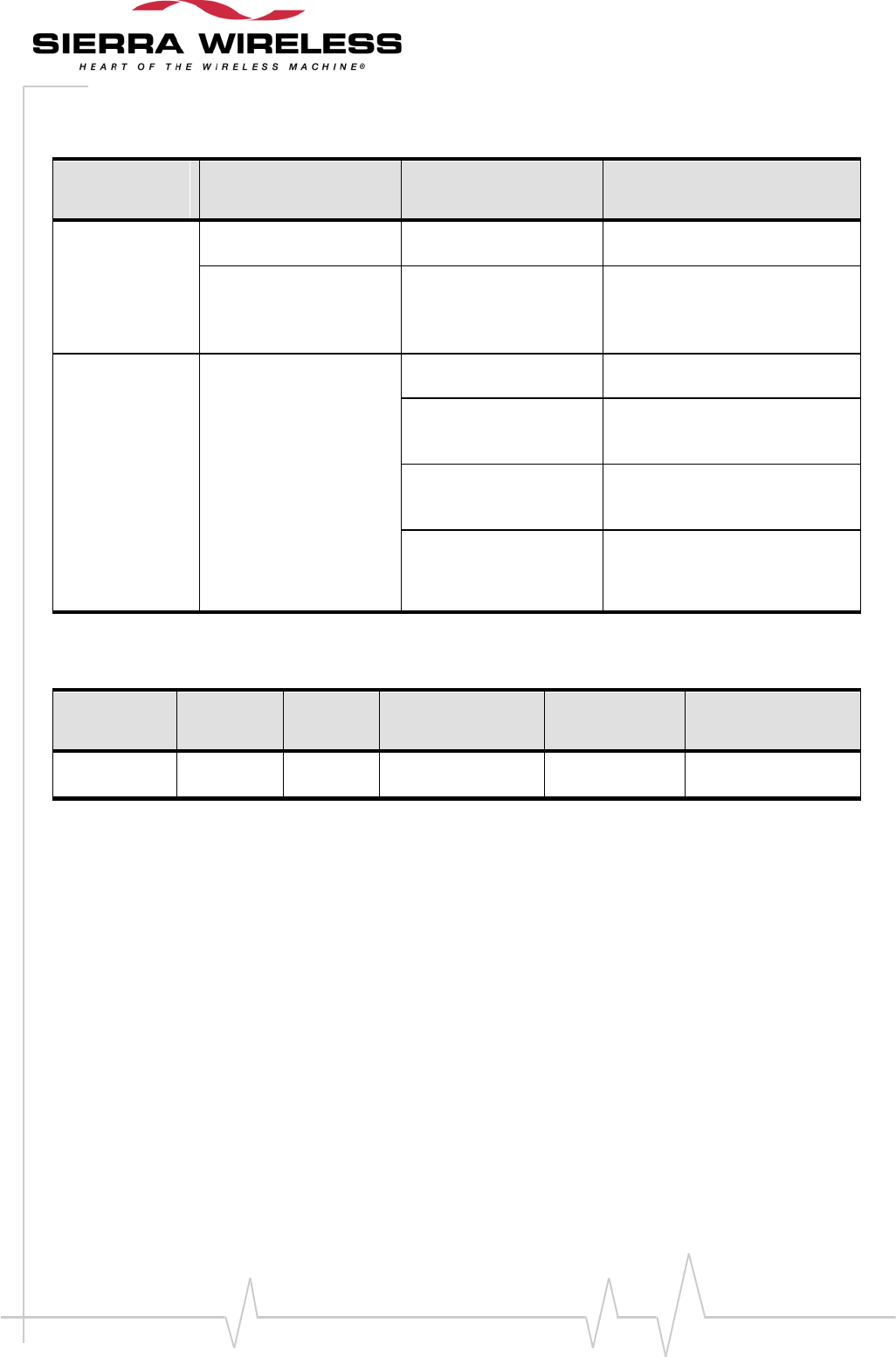
WM_DEV_Q26EX_PTS_002 Rev 006 Page 89 of 112
Product Technical Specification and
Customer Design Guidelines
Table 63. LED0 status
Wireless CPU®
state
VBATT status
LED0 status
Wireless CPU® status
Wireless CPU®
OFF
VBATT<2.8V or
VBATT> 3.2V
OFF
Wireless CPU® is OFF
2.8V < VBATT < 3.2V
Pre-charge flash
LED ON for 100 ms, OFF
for 900 ms
Wireless CPU® is OFF,
Pre-charging mode
(charger must be connected on
CHG-IN to activate this mode)
Wireless CPU®
ON
VBATT > 3.2V
Permanent
Wireless CPU® switched ON, not
registered on the network
Slow flash
LED ON for 200 ms, OFF
for 2 s
Wireless CPU® switched ON,
registered on the network
Quick flash
LED ON for 200 ms, OFF
for 600 ms
Wireless CPU® switched ON,
registered on the network,
communication in progress
Very quick flash
LED ON for 100ms, OFF
for 200ms
Wireless CPU® switched on,
software downloaded is either
corrupted or non-compatible
("BAD SOFTWARE")
Table 64. Pin description
Signal
Pin
number
I/O
I/O type
Reset state
Description
LED0
17
O
Open Drain Output
1 and
Undefined
LED driving
See Chapter Caution:, “Electrical information for digital I/O” for Open drain, 2V8 and 1V8 voltage characteristics and Reset
state definition.
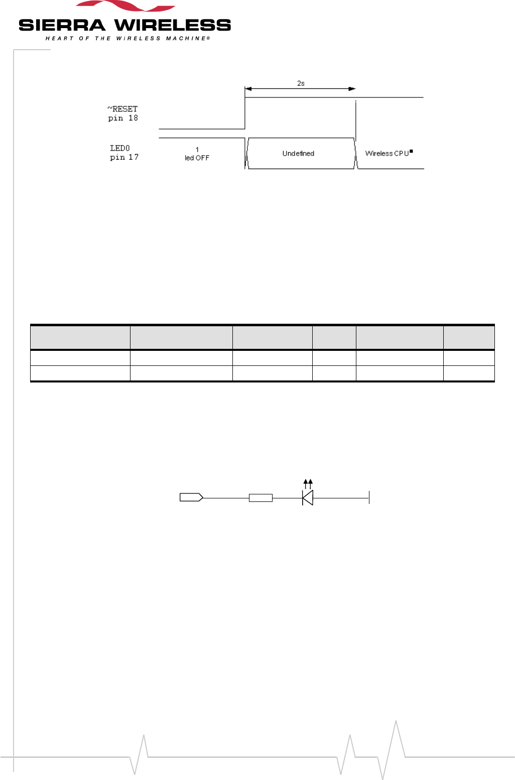
WM_DEV_Q26EX_PTS_002 Rev 006 Page 90 of 112
Product Technical Specification and
Customer Design Guidelines
Figure 45. LED0 state during RESET and Initialization time
LED0 state is high during the RESET time and undefined during the software initialization time.
During software initialization time, for 2 seconds max after RESET cancellation, the LED0 signal is
toggling and does not provide Wireless CPU® status. After the 2s period, the LED0 provides the true
status of the Wireless CPU®.
Table 65. Electrical characteristics of the signal
Parameter
Condition
Minimum
Typ
Maximum
Unit
VOL
0.4
V
IOUT
8
mA
The GSM activity status indication signals LED0 (pin 17) may be used to drive a LED. This signal is an
open-drain digital transistor in accordance to the Wireless CPU activity status.
LED0
(pin 17)VBATT
« GSM »
D1
1
2
R1
470ohms
Figure 46. Example of GSM activity status implementation
R1 value may be harmonized depending on the LED (D1) characteristics.
WM_DEV_Q26EX_PTS_002 Rev 006 Page 91 of 112
Product Technical Specification and
Customer Design Guidelines
Digital audio interface (PCM) interface mode allows connectivity with audio standard peripherals. It
can be used, for example, to connect an external audio codec.
The programmability of this mode provides the ability to address a large range of audio peripherals.
PCM features:
IOM-2 compatible device on physical level
Master mode only with 6 slots by frame, user only on slot 4
Bit rate single clock mode at 768 kHz only
16 bits data word MSB first only
Linear Law only (no compression law)
Long Frame Synchronization only
Push-pull configuration on PCM-OUT and PCM-IN
The digital audio interface configuration cannot differ from that specified above.
The PCM interface consists of 4 wires:
PCM-SYNC (output): The frame synchronization signal delivers an 8kHz frequency pulse
that synchronizes the frame data in and the frame data out.
PCM-CLK (output): The frame bit clock signal controls data transfer with the audio
peripheral.
PCM-OUT (output): The frame “data out” relies on the selected configuration mode.
PCM-IN (input): The frame “data in” relies on the selected configuration mode.
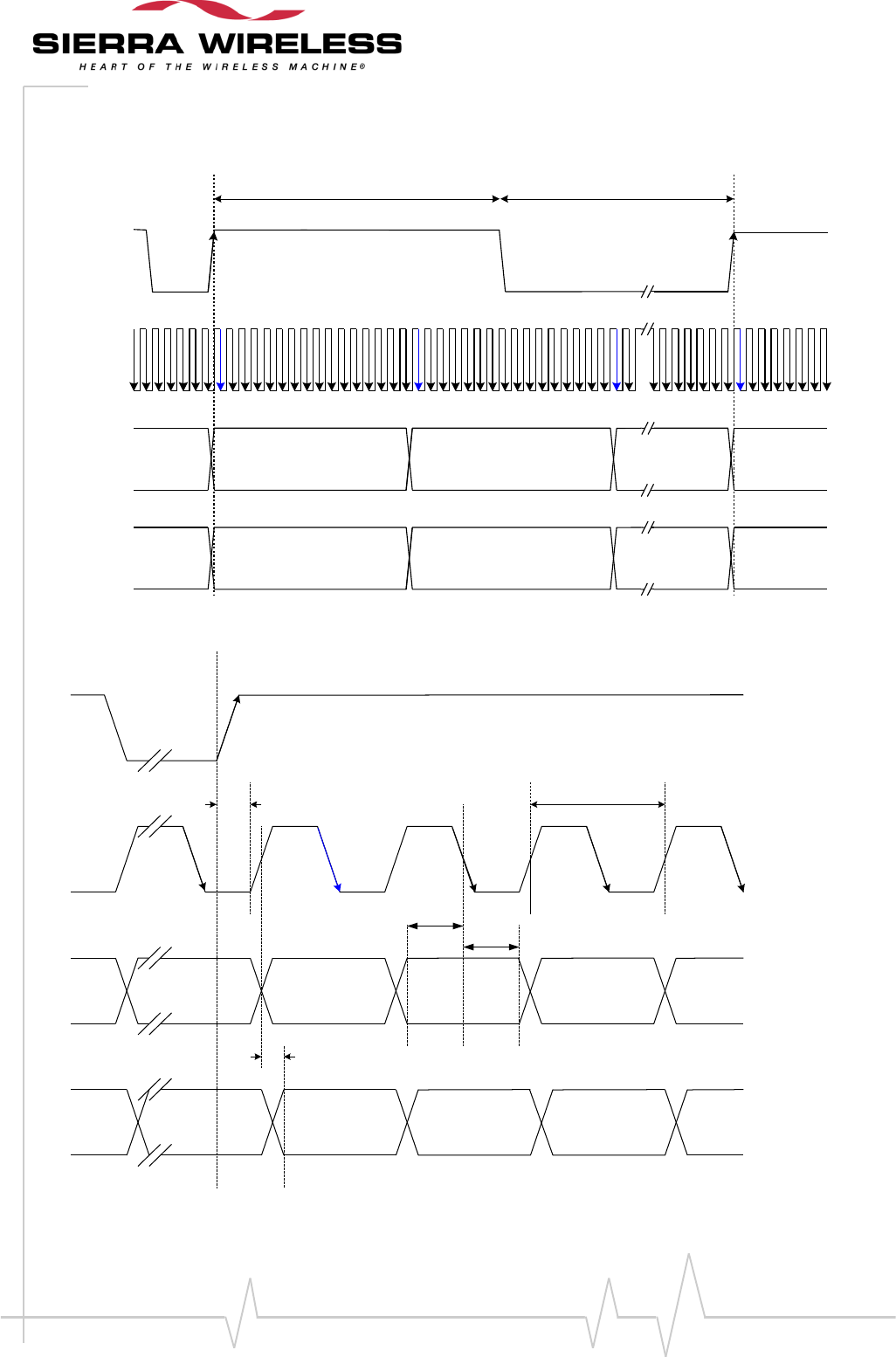
WM_DEV_Q26EX_PTS_002 Rev 006 Page 92 of 112
Product Technical Specification and
Customer Design Guidelines
SLOT 0 SLOT 1 SLOT 5 SLOT 0
SLOT 0 SLOT 1 SLOT 5 SLOT 0
SLOT 5
SLOT 5
PCM-SYNC
PCM-CLK
PCM-IN
PCM-OUT
Tsync_high Tsync_low
End of frame
Begining of
frame
Figure 47. PCM frame waveform
TOUTdelay
TSYNC-CLK
TCLK-cycle
TIN-hold
TIN-setup
PCM-SYNC
PCM-CLK
PCM-IN
PCM-OUT
SLOT 0 bit 15 SLOT 0 bit 14 SLOT 0 bit 13SLOT 5 bit 0
SLOT 0 bit 15 SLOT 0 bit 14 SLOT 0 bit 13SLOT 5 bit 0
Figure 48. PCM sampling waveform
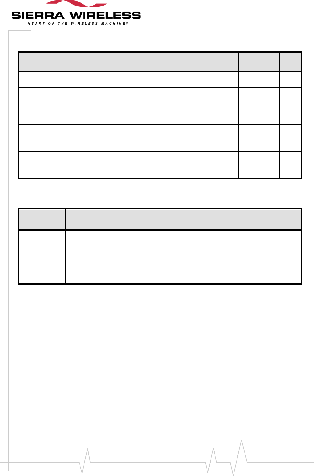
WM_DEV_Q26EX_PTS_002 Rev 006 Page 93 of 112
Product Technical Specification and
Customer Design Guidelines
Table 66. AC characteristics
Signal
Description
Minimum
Typ
Maximum
Unit
Tsync_low +
Tsync_high
PCM-SYNC period
125
µs
Tsync_low
PCM-SYNC low time
93
µs
Tsync_high
PCM-SYNC high time
32
µs
TSYNC-CLK
PCM-SYNC to PCM-CLK time
-154
ns
TCLK-cycle
PCM-CLK period
1302
ns
TIN-setup
PCM-IN setup time
50
ns
TIN-hold
PCM-IN hold time
50
ns
TOUT-delay
PCM-OUT delay time
20
ns
Table 67. Pin description of the PCM interface
Signal
Pin
number
I/O
I/O type
Reset state
Description
PCM-SYNC
77
O
1V8
Pull-down
Frame synchronization 8kHz
PCM-CLK
79
O
1V8
Pull-down
Data clock
PCM-OUT
80
O
1V8
Pull-up
Data output
PCM-IN
78
I
1V8
Pull-up
Data input
See Chapter Caution:, “Electrical information for digital I/O” for Open drain, 2V8 and 1V8 voltage characteristics and Reset
state definition.
WM_DEV_Q26EX_PTS_002 Rev 006 Page 94 of 112
Product Technical Specification and
Customer Design Guidelines
A 4-wire USB slave interface is available which complies with USB 2.0 protocol signaling. But it is not
compliant with the electrical interface, due to the 5V of VPAD-USB.
The USB interface signals are VPAD-USB, USB-DP, USB-DM and GND.
USB interface features:
12Mbit/s full-speed transfer rate
3.3V typ compatible
USB Softconnect feature
CDC 1.1 – ACM compliant
Note: A 5V to 3.3V typ voltage regulator is needed between the external interface power in line (+5V) and
the Wireless CPU® line (VPAD-USB).
Table 68. Pin description of the USB interface
Signal
Pin
number
I/O
I/O type
Description
VPAD-USB
52
I
VPAD_USB
USB Power Supply
USB-DP
54
I/O
VPAD_USB
Differential data interface positive
USB-DM
56
I/O
VPAD_USB
Differential data interface negative
Table 69. Electrical characteristics of the signals
Parameter
Min
Typ
Max
Unit
VPAD-USB, USB-DP, USB-DM
3.0
3.3
3.6
V
VPAD-USB Input current consumption
8
mA
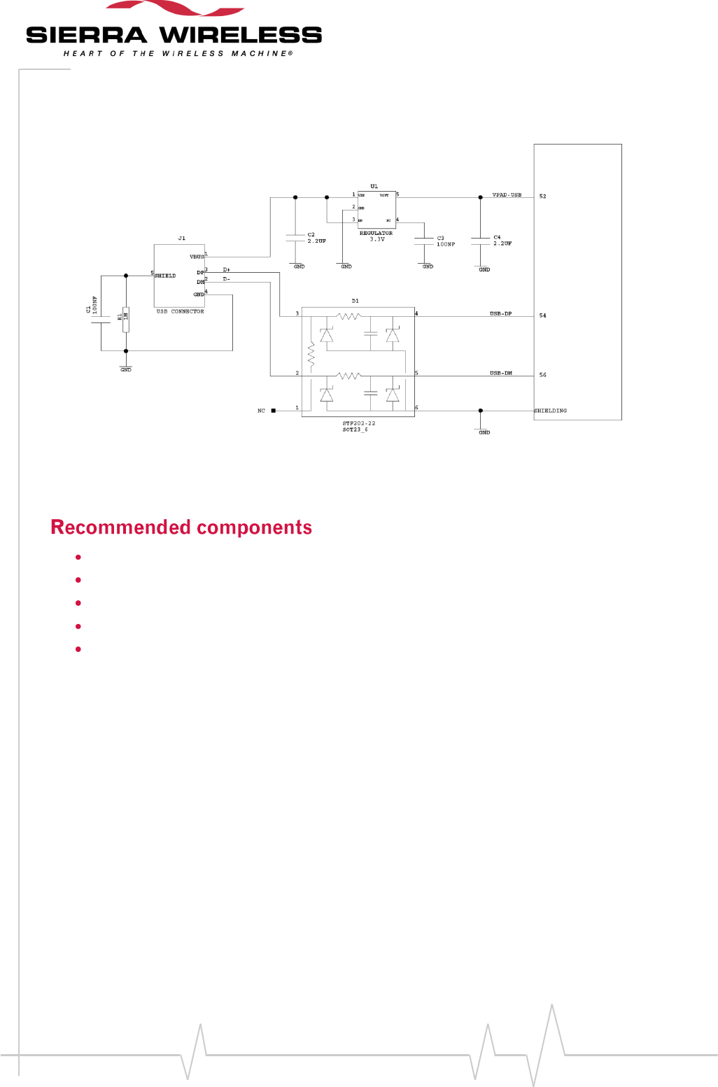
WM_DEV_Q26EX_PTS_002 Rev 006 Page 95 of 112
Product Technical Specification and
Customer Design Guidelines
Typical diagram is presented below:
Figure 49. Example of USB implementation
R1: 1MOhm
C1, C3: 100nF
C2, C4: 2.2µF
D1: STF2002-22 from SEMTECH
U1: LP2985AIM 3.3V from NATIONAL SEMICONDUCTOR
The regulator used is a 3.3V regulator. It supplies via J1 when the USB wire is plugged.
The EMI/RFI filter with ESD protection is D1. The D1 internal pull-up resistor, used to detect the full
speed, is not connected, because it is embedded in the Wireless CPU.
R1 and C1 must be close to J1.
Q26 Extreme
WM_DEV_Q26EX_PTS_002 Rev 006 Page 96 of 112
Product Technical Specification and
Customer Design Guidelines
Q26 Extreme Wireless CPU® supports two antennas (main and diversity). The impedance is 50 ohms
nominal and the DC impedance is 0 ohm.
U.FL Connector for main antenna
A wide variety of cables fitted with U.FL connectors is offered by different suppliers.
Soldered solution for main and diversity antenna
The soldered solution will preferably be based on an RG178 coaxial cable.
Note: The Q26 Extreme Wireless CPU® does not support an antenna switch for a car kit, but this function
can be implemented externally and can be driven using a GPIO.
Note: The antenna cable and connector should be selected in order to minimize losses in the frequency
bands used for GSM 850/900MHz and 1800/1900MHz.
Note: 0.5dB may be considered as the maximum value of loss between the Wireless CPU® and an external
connector.
RF performance is compliant with the ETSI GSM 05.05 recommendation.
The main Receiver parameters are:
GSM850 Reference Sensitivity = -104 dBm Static & TUHigh
E-GSM900 Reference Sensitivity = -104 dBm Static & TUHigh
DCS1800 Reference Sensitivity = -102 dBm Static & TUHigh
PCS1900 Reference Sensitivity = -102 dBm Static & TUHigh
3G Band I 2100 Reference Sensitivity = -106.7 dBm Static & TUHigh
3G Band II 1900 Reference Sensitivity = -106.7 dBm Static & TUHigh
3G Band V 850 Reference Sensitivity = -106.7 dBm Static & TUHigh
Selectivity @ 200 kHz: > +9 dBc
Selectivity @ 400 kHz: > +41 dBc
Linear dynamic range: 63 dB
Co-channel rejection: >= 9 dBc
WM_DEV_Q26EX_PTS_002 Rev 006 Page 97 of 112
Product Technical Specification and
Customer Design Guidelines
Transmitter parameters:
Maximum output power (EGSM & GSM850): 33 dBm +/- 2 dB at ambient temperature
Maximum output power (GSM1800 & PCS1900): 30 dBm +/- 2 dB at ambient temperature
Minimum output power (EGSM & GSM850): 5 dBm +/- 5 dB at ambient temperature
Minimum output power (GSM1800 & PCS1900): 0 dBm +/- 5 dB at ambient temperature
Maximum output power (3G all band): 24 dBm +1/-3 dB at ambient temperature
The antenna must meet the following requirements:
The optimum operating frequency depends on the application. Either a dual-band or quad-
band antenna will operate in these frequency bands and have the following characteristics:
Table 70. Antenna specifications
Characteristic
Q26 Extreme Wireless CPU®
E-GSM 900
DCS 1800
GSM 850 and
WCDMA band V
PCS 1900 and
WCDMA band II
WCDMA band I
TX Frequency
880 to
915 MHz
1710 to
1785 MHz
824 to
849 MHz
1850 to
1910 MHz
1920 to
1980 MHz
RX Frequency
925 to
960 MHz
1805 to
1880 MHz
869 to
894 MHz
1930 to
1990 MHz
2110 to
2170 MHz
Impedance
50
VSWR
Rx max
1.5:1
Tx max
1.5:1
Typical radiated
gain
0dBi in one direction at least
WM_DEV_Q26EX_PTS_002 Rev 006 Page 98 of 112
Product Technical Specification and
Customer Design Guidelines
Table 71. GPIO Pinout Definitions
Description
I/O*
Voltage
Signal Name
Pin
Number
Signal Name
Voltage
I/O*
Description
Mux
Nominal
Nominal
Mux
Power Supply
I
VBATT
VBATT
1
2
VBATT
VBATT
I
Power Supply
Power Supply
I
VBATT
VBATT
3
4
VBATT
VBATT
I
Power Supply
1.8V Supply
Output
O
VCC_1V8
VCC_1V8
5
6
CHG-IN
CHG-IN
I
Charger input
RTC Battery
connection
I/O
BAT-RTC
BAT-RTC
7
8
CHG-IN
CHG-IN
I
Charger input
USIM Power
Supply
O
1V8 or 3V
SIM-VCC
9
10
VCC_2V8
VCC_2V8
O
2.8V Supply
Output
USIM Data
I/O
1V8 or 3V
SIM-IO
11
12
SIMPRES
GPIO18
VCC_1V8
I
USIM Detection
USIM reset
O
1V8 or 3V
~SIM-RST
13
14
SIM-CLK
1V8 or 3V
O
USIM Clock
Buzzer Output
O
Open
Drain
BUZZER0
15
16
BOOT
VCC_1V8
I
Not Used
LED0 Output
O
Open
Drain
LED0
17
18
~RESET
VCC_1V8
I/O
RESET Input
ON / ~OFF
Control
I
VBATT
ON/~OFF
19
20
BAT-
TEMP
Analog
I
Analog
temperature
Analog to Digital
Input
I
Analog
ADC2
21
22
GPIO31
SPI1-
LOAD
VCC_2V8
I/O
SPI1 Clock
O
VCC_2V8
GPIO28
SPI1-CLK
23
24
SPI1-I
GPIO30
VCC_2V8
I
SPI1 Data Input
SPI1 Data Input
/ Output
I/O
VCC_2V8
GPIO29
SPI1-IO
25
26
SPI2-CLK
GPIO32
VCC_2V8
O
SPI2 Clock
SPI2 Data Input
/ Output
I/O
VCC_2V8
GPIO33
SPI2-IO
27
28
GPIO35
SPI2-
LOAD
VCC_2V8
I/O
SPI2 Data Input
I
VCC_2V8
GPIO34
SPI2-I
29
30
CT104-
RXD2
GPIO15
VCC_1V8
O
Auxiliary RS232
Receive
Auxiliary RS232
Transmit
I
VCC_1V8
GPIO14
CT103-
TXD2
31
32
~CT106-
CTS2
GPIO16
VCC_1V8
O
Auxiliary RS232
Clear To Send
Auxiliary RS232
Request To
Send
I
VCC_1V8
GPIO17
~CT105-
RTS2
33
34
MIC2N
Analog
I
Micro 2 Input
Negative
Speaker 1
Output Positive
O
Analog
SPK1P
35
36
MIC2P
Analog
I
Micro 2 Input
Positive
Speaker 1
Output Negative
O
Analog
SPK1N
37
38
MIC1N
Analog
I
Micro 1 Input
Negative
Speaker 2
Output Positive
O
Analog
SPK2P
39
40
MIC1P
Analog
I
Micro 1 Input
Positive
Speaker 2
Output Negative
O
Analog
SPK2N
41
42
A1
**
VCC_1V8
O
Address bus 1
I/O
VCC_2V8
32kHz
GPIO0
43
44
SCL1
GPIO26
Open
Drain
O
I²C Clock
I/O
VCC_2V8
GPIO19
45
46
SDA1
GPIO27
Open
Drain
I/O
I²C Data
I/O
VCC_2V8
GPIO21
47
48
GPIO20
VCC_2V8
I/O
Interruption 1
Input
I
VCC_2V8
GPIO25
INT1
49
50
INT0
GPIO3
VCC_1V8
I
Interruption 0
Input
WM_DEV_Q26EX_PTS_002 Rev 006 Page 99 of 112
Product Technical Specification and
Customer Design Guidelines
Description
I/O*
Voltage
Signal Name
Pin
Number
Signal Name
Voltage
I/O*
Description
I/O
VCC_1V8
**
GPIO1
51
52
VPAD-
USB
VPAD-
USB
I
USB Power
supply input
I/O
VCC_1V8
A24
GPIO2
53
54
USB-DP
VPAD-
USB
I/O
USB Data
I/O
VCC_2V8
**
GPIO23
55
56
USB-DM
VPAD-
USB
I/O
USB Data
I/O
VCC_2V8
**
GPIO22
57
58
GPIO24
VCC_2V8
I/O
Keypad
column 0
I/O
VCC_1V8
GPIO4
COL0
59
60
COL1
GPIO5
VCC_1V8
I/O
Keypad
column 1
Keypad
column 2
I/O
VCC_1V8
GPIO6
COL2
61
62
COL3
GPIO7
VCC_1V8
I/O
Keypad
column 3
Keypad
column 4
I/O
VCC_1V8
GPIO8
COL4
63
64
ROW4
GPIO13
VCC_1V8
I/O
Keypad Row 4
Keypad Row 3
I/O
VCC_1V8
GPIO12
ROW3
65
66
ROW2
GPIO11
VCC_1V8
I/O
Keypad Row 2
Keypad Row 1
I/O
VCC_1V8
GPIO10
ROW1
67
68
ROW0
GPIO9
VCC_1V8
I/O
Keypad Row 0
Main RS232
Ring Indicator
O
VCC_2V8
GPIO42
~CT125-
RI
69
70
~CT109-
DCD1
GPIO43
VCC_2V8
O
Main RS232
Data Carrier
Detect
Main RS232
Transmit
I
VCC_2V8
GPIO36
CT103-
TXD1
71
72
~CT105-
RTS1
GPIO38
VCC_2V8
I
Main RS232
Request To
Send
Main RS232
Receive
O
VCC_2V8
GPIO37
CT104-
RXD1
73
74
~CT107-
DSR1
GPIO40
VCC_2V8
O
Main RS232
Data Set Ready
Main RS232
Clear To Send
O
VCC_2V8
GPIO39
~CT106-
CTS1
75
76
~CT108-2-
DTR1
GPIO41
VCC_2V8
I
Main RS232
Data Terminal
Ready
PCM Frame
Synchro
O
VCC_1V8
PCM-
SYNC
77
78
PCM-IN
VCC_1V8
I
PCM Data Input
PCM Clock
O
VCC_1V8
PCM-CLK
79
80
PCM-OUT
VCC_1V8
O
PCM Data
Output
Read enable
VCC_1V8
~OE-R/W
81
82
DAC0
Analog
O
Chip select 3
VCC_1V8
GPIO44/
~CS3
83
84
~WE-E
VCC_1V8
Write enable
DATA bus
VCC_1V8
D0
85
86
D15
VCC_1V8
DATA bus
DATA bus
VCC_1V8
D1
87
88
D14
VCC_1V8
DATA bus
DATA bus
VCC_1V8
D2
89
90
D13
VCC_1V8
DATA bus
DATA bus
VCC_1V8
D3
91
92
D12
VCC_1V8
DATA bus
DATA bus
VCC_1V8
D4
93
94
D11
VCC_1V8
DATA bus
DATA bus
VCC_1V8
D5
95
96
D10
VCC_1V8
DATA bus
DATA bus
VCC_1V8
D6
97
98
D9
VCC_1V8
DATA bus
DATA bus
VCC_1V8
D7
99
100
D8
VCC_1V8
DATA bus
* The I/O direction information is only for the nominal signal. When the signal is configured in GPIO, it can always be an
Input or an Output.
** For more information about the multiplexing of these signals, see “General purpose
input /output”, section 0
WM_DEV_Q26EX_PTS_002 Rev 006 Page 100 of 112
Product Technical Specification and
Customer Design Guidelines
Wavecom specifies the following temperature range for the Q26 Extreme Wireless CPU® product.
The Q26 Extreme Wireless CPU® is compliant with the following operating class.
Table 72. Operating Temperatures
Conditions
Temperature range
Operating / Class A
-20 °C to +55°C
Operating / Storage / Class B
-30 °C to +75°C
Function Status Classification:
Class A:
The Wireless CPU® remains fully functional, meeting GSM performance criteria in accordance with
ETSI requirements, across the specified temperature range.
Class B:
Operating Class B restrictions depends on Q26 Extreme implementation; refer to section 6.1.1 for
optimized implementation,
The Wireless CPU® remains functional, across the specified temperature range. Some GSM
parameters may occasionally deviate from the ETSI specified requirements. Auto shut down is
implemented for protection against extreme temperature (deactivated for emergency calls), refer table
for communication characteristic in extreme T° environment.
The table below show sample measurements in lab environment conditions (Environmental
specifications will be available after Q26 Extreme environmental qualification plan).Operating
duration versus temperature
Table 73. Operating duration versus temperature
Mode
Ambient
temperature (°C)
RF Power
(dBm)
Operating
duration (min)
GSM/GPRS/EGPRS Class 8
75
Max
GPRS/EGPRS Class 10
70
Max
GPRS/EGPRS Class 10
75
Max
1
GPRS/EGPRS Class 12
65
Max
GPRS/EGPRS Class 12
70
Max
2
WCDMA
70
< 0
WCDMA
65
Max
WCDMA
70
Max
2
HSDPA 7.2 Mbits/s
70
< 0
HSDPA 7.2 Mbits/s
60
Max
WM_DEV_Q26EX_PTS_002 Rev 006 Page 101 of 112
Product Technical Specification and
Customer Design Guidelines
Mode
Ambient
temperature (°C)
RF Power
(dBm)
Operating
duration (min)
HSDPA 7.2 Mbits/s
65
Max
2
Test condition: Q26 Extreme plug in a starter kit light with forced air circulation Vbatt = 3.8V. (See 0
for starter kit light picture.)
The Q26 Extreme Wireless CPU® has a complete self-contained shield.
Overall dimensions : 32.2x40x6.3 mm (except shielding pins)
Weight : 11,8 g
The mechanical specifications of the Q26 Extreme Wireless CPU® are shown in the following page.
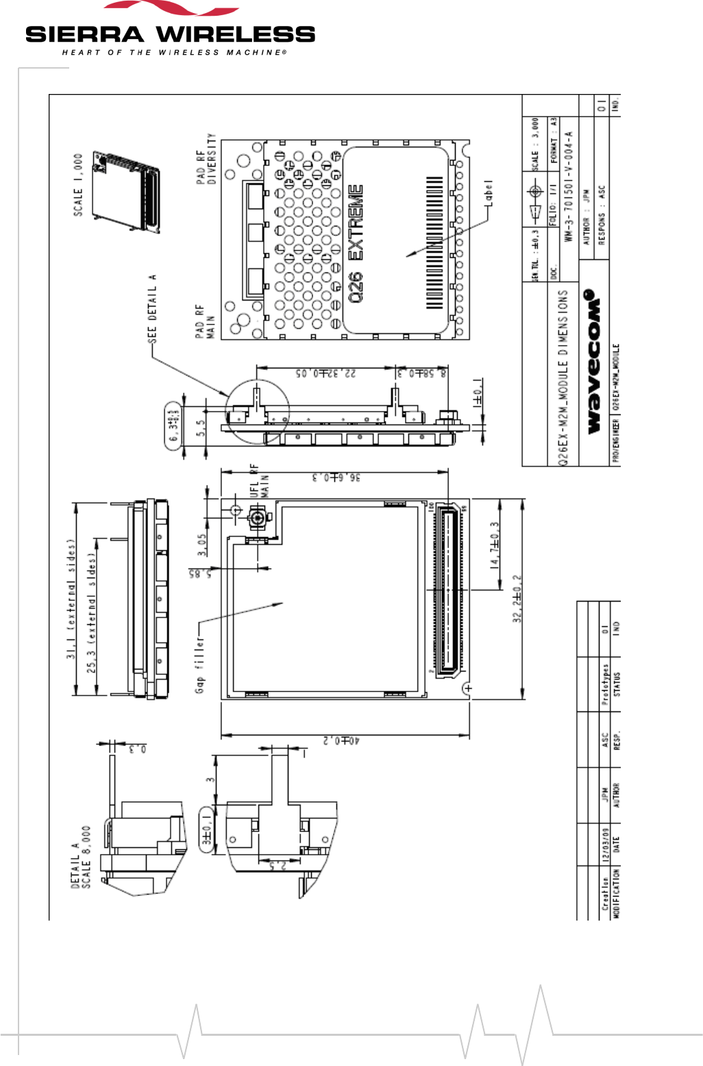
WM_DEV_Q26EX_PTS_002 Rev 006 Page 102 of 112
Product Technical Specification and
Customer Design Guidelines
Figure 50. Mechanical drawing
WM_DEV_Q26EX_PTS_002 Rev 006 Page 103 of 112
Product Technical Specification and
Customer Design Guidelines
The GPC is a 100-pin connector with 0.5mm pitch from the from PANASONIC Group's P5K series,
with the following reference:
AXK600347BN1
The matting connector has the following reference:
AXK500147BN1J
The stacking height is 3.0 mm.
Wavecom recommends that you use the AXK500147BN1J connector for your application to benefit
from Wavecom prices. For more information, contact Wavecom, specifying the Wavecom connector
reference: WM18868.
For further details see the GPC data sheets in the appendix. More information is also available from:
AMPHENOL C707 series (see )
JAE (see )
MOLEX 99228-0002 (connector) / MOLEX 91236-0002 (holder) (see )
Possible suppliers:
HOSIDEN
PANASONIC
PEIKER
WM_DEV_Q26EX_PTS_002 Rev 006 Page 104 of 112
Product Technical Specification and
Customer Design Guidelines
Possible suppliers:
SANYO
HOSIDEN
PRIMO
PHILIPS
There is a main connection for 2G and 3G and a diversity connection only for 3G.
For the main connection we have two possibilities:
UF-L pigtails connection on the bottom side
Coaxial cable soldered to the RF pad (opposite side of the UF-L connector) on the top side
For the diversity connection the only possibility is to solder a coaxial cable to the second RF pad (no
UF-L connector on the opposite side) on the top side.
A wide variety of cables fitted with UF-L connectors is offered by HIROSE:
UF-L pigtails, Ex: Ref = U.FL-2LP(V)-04-A-(100)
UF-L Ref = U.FL-R-SMT
UF-L cable assemblies,
Between series cable assemblies.
More information is also available from .
For the coaxial cable soldered on the RF pad the following references have been certified for
mounting on the Q26 Extreme Wireless CPU®:
RG178
RG316
RF antennas and support for antenna adaptation can be obtained from manufacturers such as:
TAOGLAS ( )
HIRSCHMANN ( )
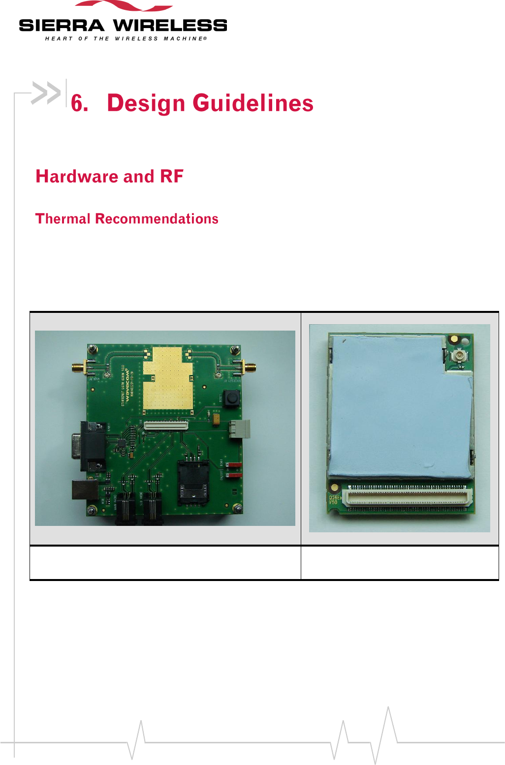
WM_DEV_Q26EX_PTS_002 Rev 006 Page 105 of 112
Product Technical Specification and
Customer Design Guidelines
The purpose of the following paragraphs is to present design guidelines.
The Q26 Extreme is natively equipped with a foam improving thermal dissipation for a better
behavior in extreme conditions.
In order to improve thermal dissipation in the customer board, it is recommended to add a copper
area (without solder mask) on both side of the customer PCB. Both sides shall be connected with
thermal via.
Starter kit used for thermal behavior measurement
with Copper Area
Foam mounted on Q26 Extreme
Figure 51. Thermal foam mounting
WM_DEV_Q26EX_PTS_002 Rev 006 Page 106 of 112
Product Technical Specification and
Customer Design Guidelines
The EMC tests must be performed on the application as soon as possible to detect any potential
problems.
When designing, special attention should be paid to:
Possible spurious emission radiated by the application to the RF receiver in the receiver band
ESD protection is mandatory on all signals which have external accessibility (typically human
accessibility).
Typically, ESD protection is mandatory for the:
USIM (if accessible from outside)
Serial link
EMC protection on audio input/output (filters against 900MHz emissions)
Biasing of the microphone inputs
Length of the USIM interface lines (preferably <10cm)
Ground plane: Wavecom recommends a common ground plane for analog/digital/RF
grounds.
A metallic case or plastic casing with conductive paint are recommended
Note: The Wireless CPU® does not include any protection against over-voltage.
The power supply is one of the key issues in the design of a terminal.
A weak power supply design could, in particular, affect:
EMC performance
The emission spectrum
The phase error and frequency error
Warning: Careful attention should be paid to:the quality of the power supply:
low ripple, PFM or PSM systems should be avoided (PWM converter
preferred), and the capacity to deliver high current peaks in a short
time (pulsed radio emission).
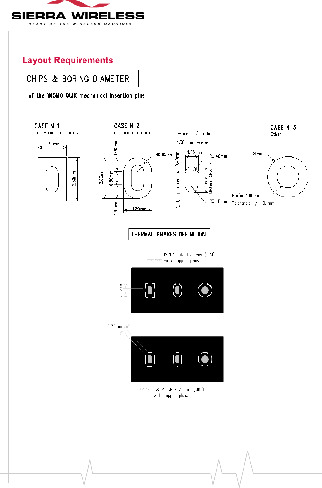
WM_DEV_Q26EX_PTS_002 Rev 006 Page 107 of 112
Product Technical Specification and
Customer Design Guidelines
Figure 52. Layout requirement
WM_DEV_Q26EX_PTS_002 Rev 006 Page 108 of 112
Product Technical Specification and
Customer Design Guidelines
Warning: Wavecom strongly recommends working with an antenna
manufacturer either to develop an antenna adapted to the
application or to adapt an existing solution to the application.
Both the mechanical and electrical antenna adaptation is one of the
key issues in the design of the GSM/UMTS terminal.
Attention should be paid to:
Antenna cable integration (bending, length, position, etc)
Leads of the Wireless CPU® to be soldered to the Ground plane
The Q26 Extreme Wireless CPU® Operating System is stored in flash memory and can easily be
upgraded.
Caution: In order to follow regular changes in the 3GPP standard and to offer a state-of-the-art Operating
System, Wavecom recommends that the application designed around a Wireless CPU® (or
Wireless CPU® based product) allow easy Operating System upgrades on the Wireless CPU®
via the standard X-modem protocol. Therefore, the application shall either allow a direct access
to the Wireless CPU® serial link through an external connector or implement any mechanism
allowing the Wireless CPU® Operating System to be downloaded via X-modem.
The Operating System file can be downloaded to the modem using the X-modem protocol. The
AT+WDWL command allows the download process to be launched (see the description in the AT
Command User Guide [5]).
The serial signals required to proceed with X-modem downloading are:
Rx, Tx, RTS, CTS and GND.
The Operating System file can also be downloaded to the modem using the DOTA (download over
the air) feature. This feature is available with the Open AT® interface. For more details, please, refer to
the Open AT® documentation 0.
WM_DEV_Q26EX_PTS_002 Rev 006 Page 109 of 112
Product Technical Specification and
Customer Design Guidelines
The Q26 Extreme Wireless CPU® connected on a development kit board application is compliant with
the following requirements:
R&TTE:
Spectrum: EN 301 511 v 9.0.2
Safety: EN 60950-1:2005 (Ed 2.0)
EMC: EN 301 489-1v 1.8.1, EN 301 489-7 v1.3.1, EN 301 489-24 v1.4.1
GCF-CC and NAPRD.03 versions will be specified as soon as certification will be started
(most updated version applicable at this time)
Federal Communications Commission (FCC) rules and Regulations: Power listed on the Grant is
conducted for Part 22 and conducted for Part 24
This device is to be used only for mobile and fixed applications. The antenna(s) used for this
transmitter must be installed to provide a separation distance of at least 20cm from all persons and
must not be co-located or operating in conjunction with any other antenna or transmitter within a
host device, except in accordance with FCC multi-transmitter product procedures.
Antennas used for this OEM module must not exceed a gain of 4.6dBi (850MHz) and 3.4dBi
(1900MHz) respectively. This device is approved as a module to be installed in other devices.
Installed in other portable devices, the exposure conditions require a separate equipment
authorization.
The license module had a FCC ID label on the module itself. The FCC ID label must be visible
through a window or it must be visible when an access panel, door or cover is easily removed.
If not, a second label must be placed on the outside of the device that contains the following text:
Contains FCC ID: O9EQ26EX
This device complies with Part 15 of the FCC Rules. Operation is subject to the following two
conditions:
this device may not cause harmful interference,
this device must accept any interference received, including interference that may cause
undesired operation.
Caution: Manufacturers of mobile or fixed devices incorporating Q26 Extreme Wireless CPU® are
advised to clarify any regulatory questions, have their completed product tested, have product
approved for FCC compliance, and include instructions according to above mentioned RF
exposure statements in end product user manual.
Please note that changes or modifications not expressly approved by the party responsible for
compliance could void the user’s authority to operate the equipment.
WM_DEV_Q26EX_PTS_002 Rev 006 Page 110 of 112
Product Technical Specification and
Customer Design Guidelines
For the efficient and safe operation of your GSM device, please read the following information
carefully.
Your GSM terminal is based on the GSM standard for cellular technology. The GSM standard is
spread all over the world. It covers Europe, Asia and some parts of America and Africa. This is the
most used telecommunication standard.
Your GSM terminal is actually a low power radio transmitter and receiver. It sends out as well as
receives radio frequency energy. When you use your GSM application, the cellular system which
handles your calls controls both the radio frequency and the power level of your cellular modem.
There has been some public concern on possible health effects of using GSM terminals. Although
research on health effects from RF energy has focused on the current RF technology for many years,
scientists have begun research regarding newer radio technologies, such as GSM. After existing
research had been reviewed, and after compliance to all applicable safety standards had been tested,
it has been concluded that the product was fitted for use.
If you are concerned about exposure to RF energy there are things you can do to minimize exposure.
Obviously, limiting the duration of your calls will reduce your exposure to RF energy. In addition,
you can reduce RF exposure by operating your cellular terminal efficiently by following the
guidelines below.
For your GSM terminal to operate at the lowest power level, consistent with satisfactory call quality:
If your terminal has an extendable antenna, extend it fully. Some models allow you to place a call
with the antenna retracted. However your GSM terminal operates more efficiently with the antenna
when it is fully extended.
Do not hold the antenna when the terminal is "IN USE". Holding the antenna affects call quality and
may cause the modem to operate at a higher power level than needed.
Do not use the GSM terminal with a damaged antenna. If a damaged antenna comes into contact with
the skin, a minor burn may result. Replace a damaged antenna immediately. You may repair antenna
to yourself by following the instructions provided to you. If so, use only a manufacturer-approved
antenna. Otherwise, have your antenna repaired by a qualified technician.
WM_DEV_Q26EX_PTS_002 Rev 006 Page 111 of 112
Product Technical Specification and
Customer Design Guidelines
Buy or replace the antenna only from the approved suppliers list. Using of unauthorized antennas,
modifications or attachments could damage the terminal and may violate local RF emission
regulations or invalidate type approval.
Check the laws and the regulations regarding the use of cellular devices in the area where you have to
drive as you always have to comply with them. When using your GSM terminal while driving,
please:
give full attention to driving,
pull-off from the road and park before making or answering a call if driving conditions so
require.
Most electronic equipment, for example in hospitals and motor vehicles is shielded from RF energy.
However, RF energy may affect some improperly shielded electronic equipment.
Check your vehicle manufacturer representative to determine if any on-board electronic equipment is
adequately shielded from RF energy.
Consult the manufacturer of any personal medical devices (such as pacemakers, hearing aids, etc) to
determine if they are adequately shielded from external RF energy.
Turn your terminal OFF in health care facilities when any regulations posted in the area instruct you
to do so. Hospitals or health care facilities may be using RF monitoring equipment.
Turn your terminal OFF before boarding any aircraft.
Use it on the ground only with crew permission.
Do not use it in the air.
To prevent possible interference with aircraft systems, Federal Aviation Administration (FAA)
regulations require you should have prior permission from a crew member to use your terminal
while the aircraft is on the ground. In order to prevent interference with cellular systems, local RF
regulations prohibit using your modem while airborne.
WM_DEV_Q26EX_PTS_002 Rev 006 Page 112 of 112
Product Technical Specification and
Customer Design Guidelines
Do not allow children to play with your GSM terminal. It is not a toy. Children could hurt themselves
or others (by poking themselves or others in the eye with the antenna, for example). Children could
damage the modem, or make calls that increase your modem bills.
To avoid interfering with blasting operations, turn your unit OFF when you are in a "blasting area" or
in areas posted: "turn off two-way radio". Construction crew often uses remote control RF devices to
set off explosives.
Turn your terminal OFF when in any area with a potentially explosive atmosphere. Though it is rare,
but your modem or its accessories could generate sparks. Sparks in such areas could cause an
explosion or fire resulting in bodily injuries or even death.
Areas with a potentially explosive atmosphere are often, but not always, clearly marked. They
include fuelling areas such as petrol stations; below decks on boats; fuel or chemical transfer or
storage facilities; and areas where the air contains chemicals or particles, such as grain, dust, or metal
powders.
Do not transport or store flammable gas, liquid, or explosives, in the compartment of your vehicle
which contains your terminal or accessories.
Before using your terminal in a vehicle powered by liquefied petroleum gas (such as propane or
butane) ensure that the vehicle complies with the relevant fire and safety regulations of the country in
which the vehicle is used.
