Sierra Wireless Q52OMNI Dual mode transceiver User Manual
Sierra Wireless, Inc. Dual mode transceiver
UserManual.wiki
>
Sierra Wireless
>
Q52OMNI User Manual
User Manual
Navigation menu
Upload a User Manual
Namespaces
Wiki Guide
HTML
PDF
Info
Views
User Manual
Discussion / Help
Navigation


![Q52 Omni Product Technical Specification © Confidential Page 11 / 78 This document is the sole and exclusive property of WAVECOM. Not to be distributed or divulged without prior written agreement. 1 References 1.1 Reference Documents For more details, several reference documents may be consulted. The Wavecom reference documents are provided in the Wavecom document package, contrary to the general reference documents which are not authored by Wavecom. 1.1.1 Wavecom Reference Documentation [1] Wireless Microprocessor® WMP100 Technical Specification Reference: WM_DEV_WUP_PTS_004 [2] WMP100 Development Kit User Guide Reference: WM_DEV_WUP_UGD_001 [3] AT Command Interface Guide for Open AT® Firmware v7.0 Reference: WM_DEV_OAT_UGD_059 1.1.2 General Reference Documents [4] “I²C Bus Specification”, Version 2.0, Philips Semiconductor 1998 [5] ISO 7816-3 Standard](https://usermanual.wiki/Sierra-Wireless/Q52OMNI/User-Guide-1038962-Page-12.png)
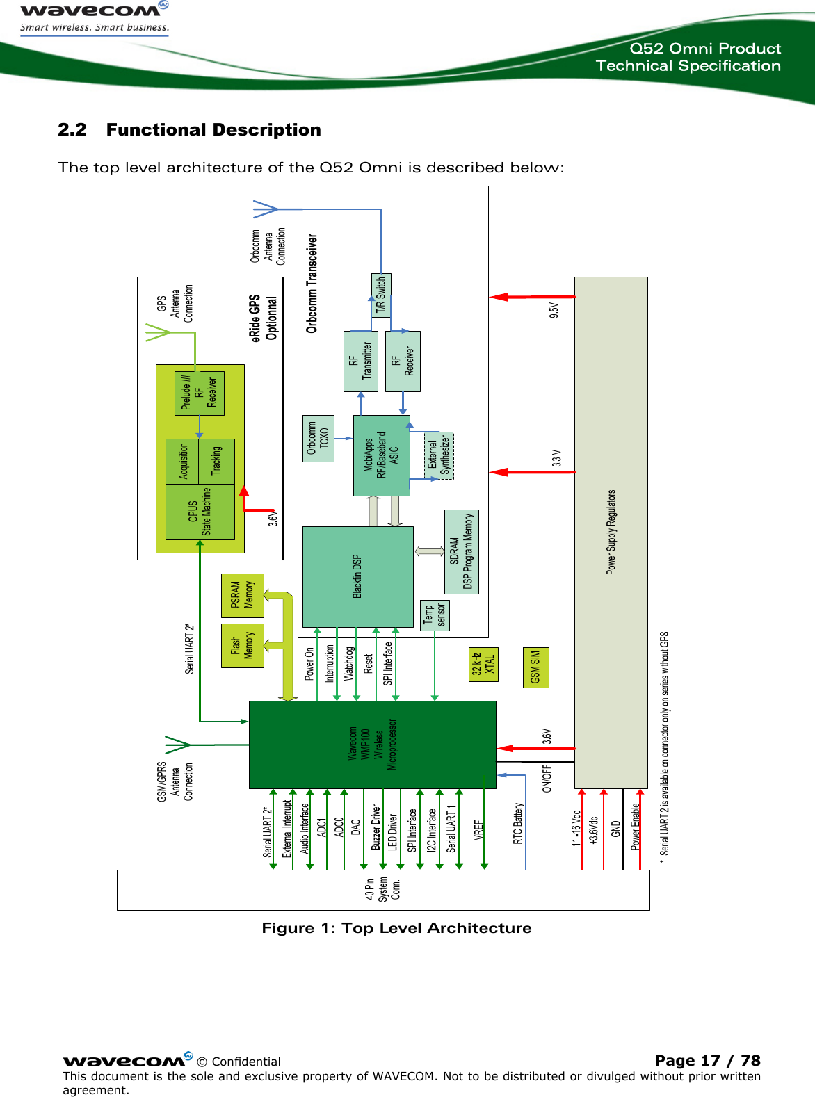


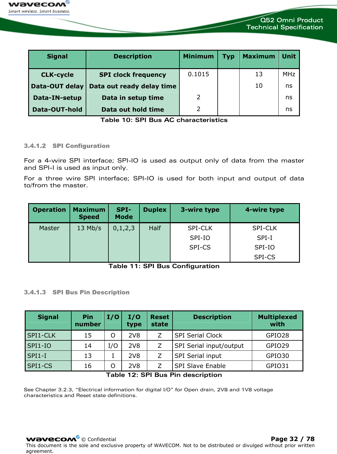
![Q52 Omni Product Technical Specification © Confidential Page 29 / 78 This document is the sole and exclusive property of WAVECOM. Not to be distributed or divulged without prior written agreement. 3.2.3 Recommendations for Less Consumption For a better consumption, in particular for the quiescent current, it is recommended to drive the GPIOs like show in the table below. Signal Muxed with I/O I/O type Reset state SW driver recommended (output state) GPIO14* TXD2 I/O 1V8 Z 0 logic level GPIO15* RXD2 I/O 1V8 Z 0 logic level GPIO16* CTS2 I/O 1V8 Z 0 logic level GPIO17* RTS2 I/O 1V8 Z 0 logic level GPIO24 HW-SD I/O 2V8 Z 0 logic level GPIO26 SCL I/O Open drain Z 0 logic level GPIO27 SDA I/O Open drain Z 0 logic level GPIO28 SPI1-CLK I/O 2V8 Z 0 logic level GPIO29 SPI1-IO I/O 2V8 Z 0 logic level GPIO30 SPI1-I I/O 2V8 Z 0 logic level GPIO31 SPI1-CS I/O 2V8 Z 0 logic level GPIO46 EXT-INT I/O 2V8 Z 0 logic level * If available If the FLASH-LED are not necessary it is possible to disable them. For further details refer to document [3] AT Command Interface Guide for Open AT® Firmware v7.0).](https://usermanual.wiki/Sierra-Wireless/Q52OMNI/User-Guide-1038962-Page-30.png)
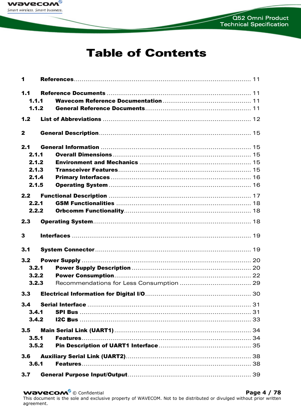
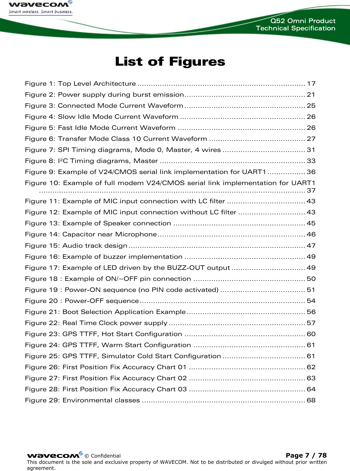
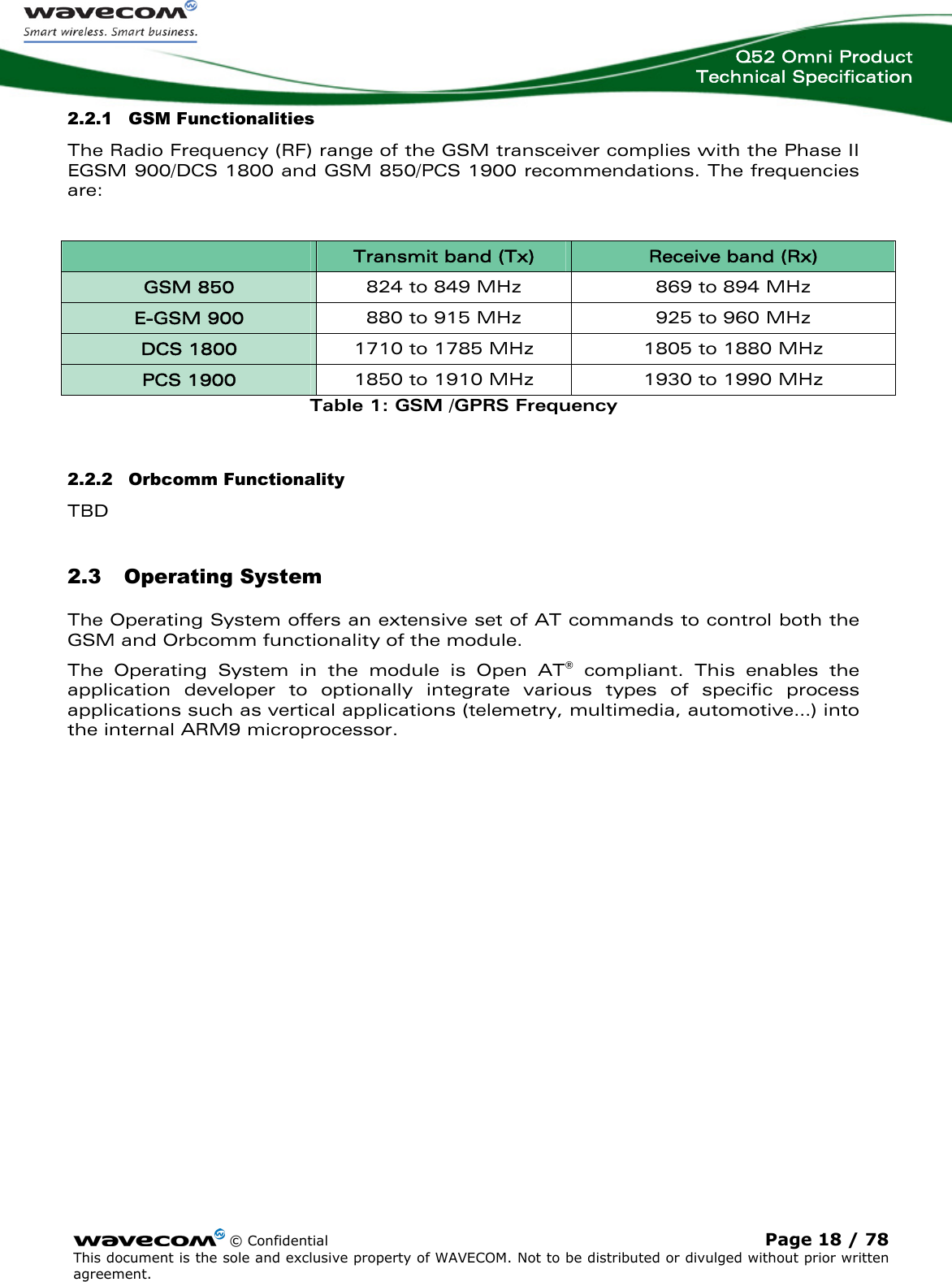
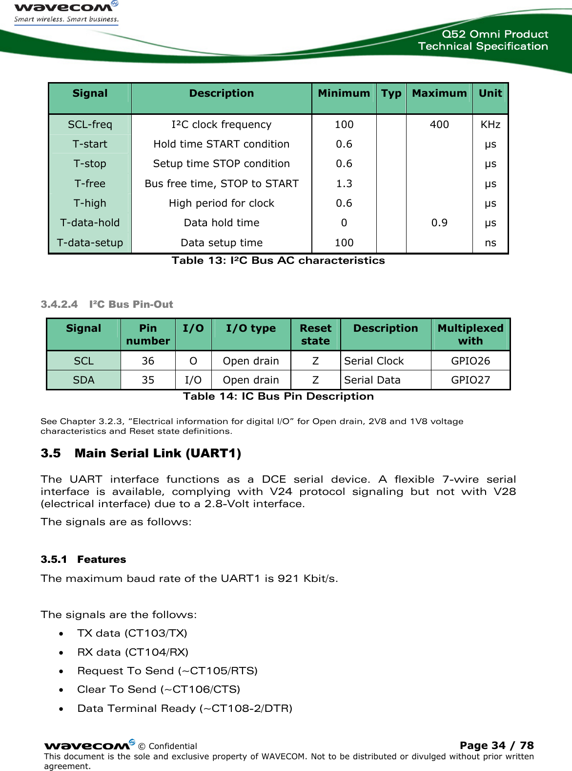
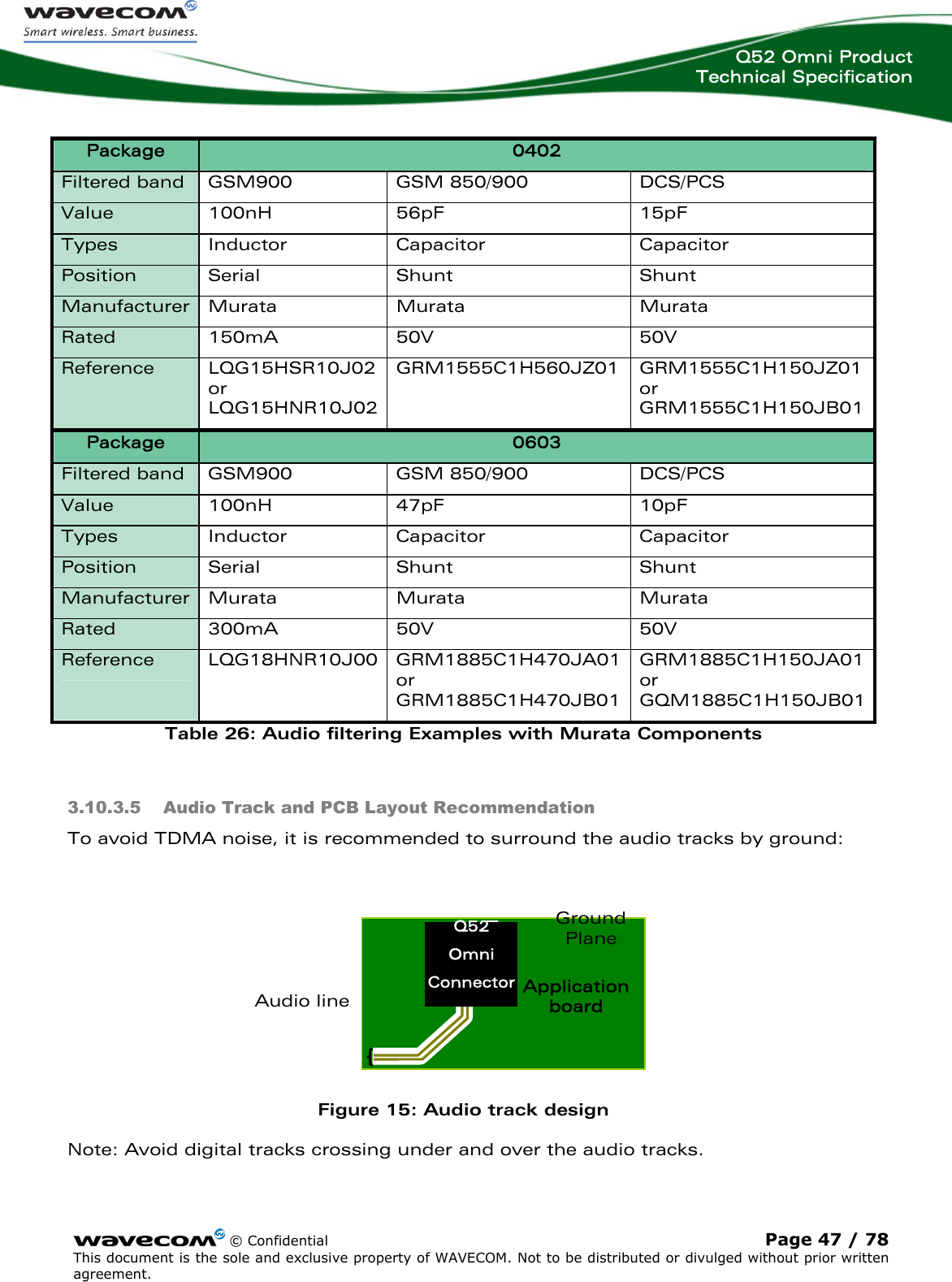
![Q52 Omni Product Technical Specification © Confidential Page 33 / 78 This document is the sole and exclusive property of WAVECOM. Not to be distributed or divulged without prior written agreement. Data valid3.4.2 I2C Bus 3.4.2.1 Features The I2C interface includes a clock signal (SCL) and data signal (SDA) complying with a 100Kbit/s-standard interface (standard mode: s-mode). 3.4.2.2 Characteristics The I²C bus is always master. The maximum speed transfer range is 400Kbit/s (fast mode: f-mode). For more information on the bus, see the [4]“I²C Bus Specification”, Version 2.0, Philips Semiconductor 19983.4.2.3 I²C Waveforms I²C bus waveform in master mode configuration: SCLSDAData validT-freeT-startT-highT-data-setupT-data-holdT-stopSCL-freq Figure 8: I²C Timing diagrams, Master](https://usermanual.wiki/Sierra-Wireless/Q52OMNI/User-Guide-1038962-Page-34.png)
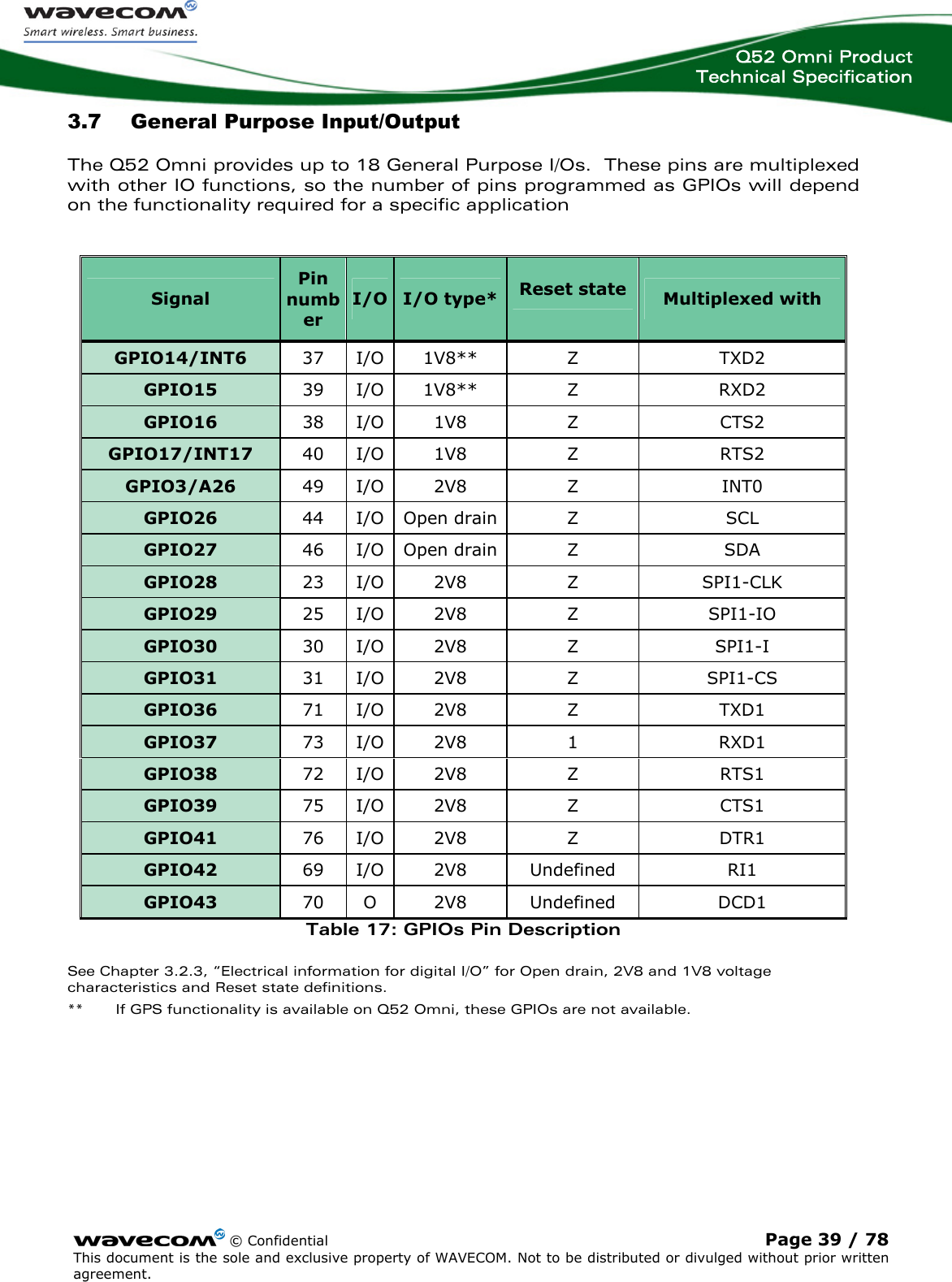
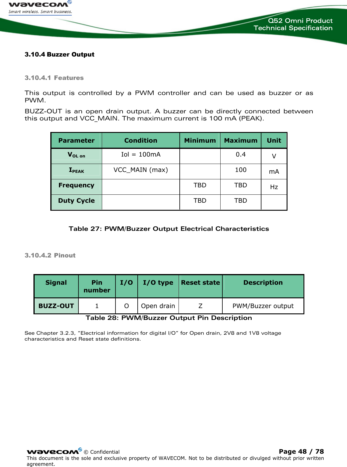
![Q52 Omni Product Technical Specification © Confidential Page 35 / 78 This document is the sole and exclusive property of WAVECOM. Not to be distributed or divulged without prior written agreement. • Data Carrier Detect (~CT109/DCD) • Ring Indicator (~CT125/RI). 3.5.2 Pin Description of UART1 Interface Table 15: UART1 Pin Description * According to PC view See Wireless Microprocessor® WMP100 Technical Specification for Open drain, 2V8 and 1V8 voltage characteristics and for Reset state definition. The rise and fall time of the reception signals (mainly TXD_UART1) must be less than 300 ns. The Q52 Omni is designed to operate using all the serial interface signals. In particular, it is mandatory to use RTS and CTS for hardware flow control in order to avoid data corruption during transmission. For the use case with 5-wire serial interface • Signal: CT103/TXD1*, CT104/RXD1*, ~CT105/RTS1*, ~CT106/CTS1* • The signal ~CT108-2/DTR1* must be managed following the V24 protocol signalling if we want to use the slow idle mode • The other signals and their multiplexed are not available • Please refer to the document [3] AT Command Interface Guide for Open AT® Firmware v7.0 for more information. Signal Pin number I/O I/O type Reset state Description Multiplexed with CT103/TXD1* 27 I 2V8 Z Transmit serial data GPIO36 CT104/RXD1* 30 O 2V8 1 Receive serial data GPIO37 ~CT105/RTS1* 28 I 2V8 Z Request To Send GPIO38 ~CT106/CTS1* 25 O 2V8 Z Clear To Send GPIO39 ~CT108-2/DTR1* 26 I 2V8 Z Data Terminal Ready GPIO41 ~CT109/DCD1* 23 O 2V8 Undefined Data Carrier Detect GPIO43 ~CT125/RI1* 24 O 2V8 Undefined Ring Indicator GPIO42 CT102/GND* Chassis GND GND Ground](https://usermanual.wiki/Sierra-Wireless/Q52OMNI/User-Guide-1038962-Page-36.png)
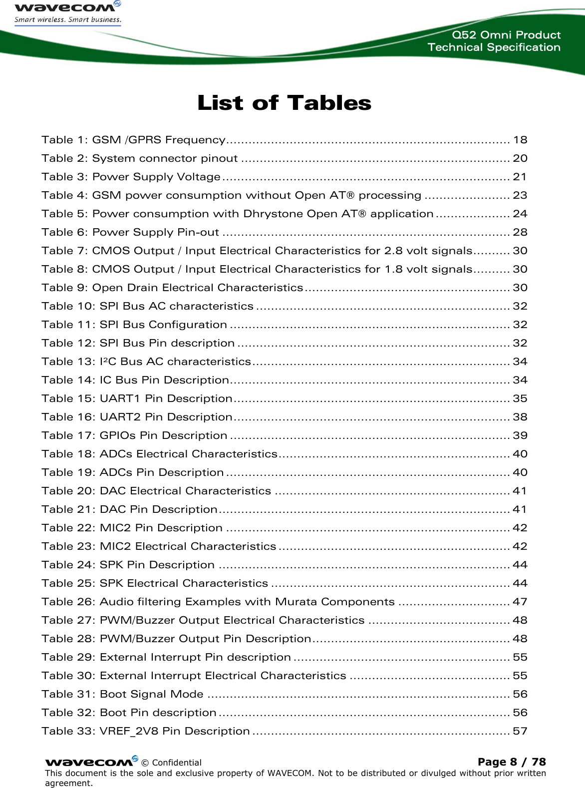
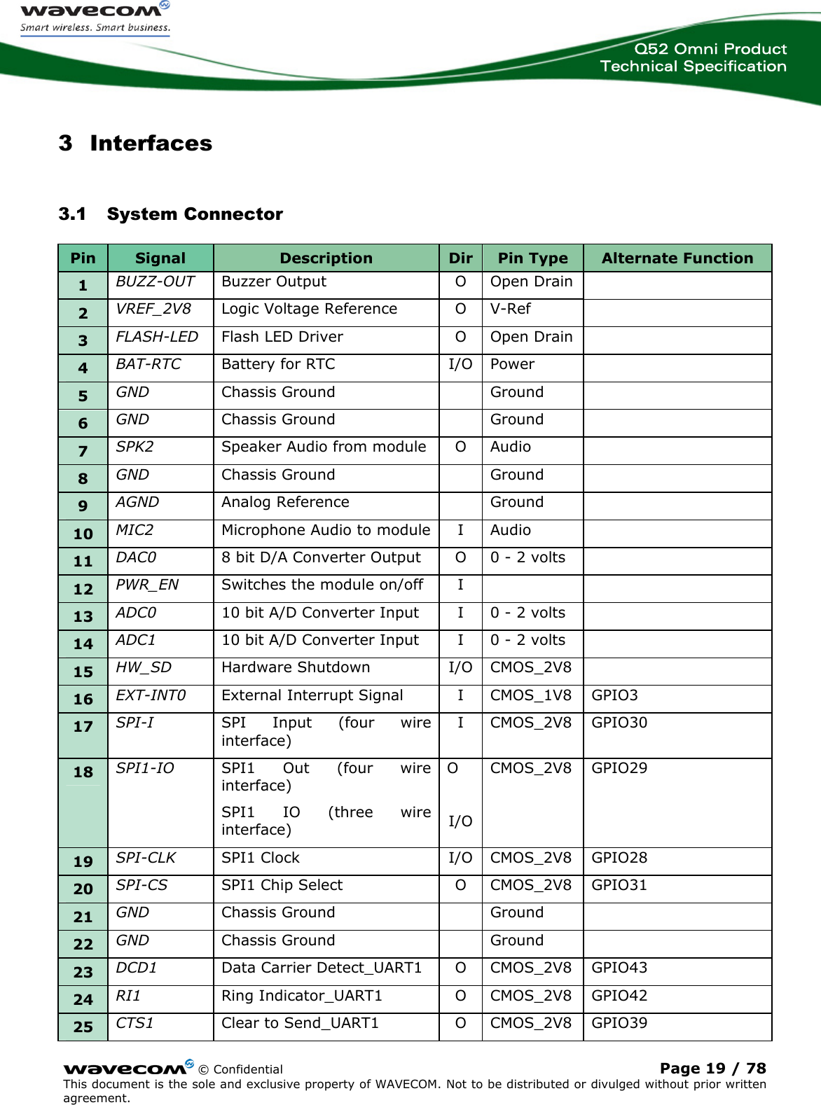
![Q52 Omni Product Technical Specification For the use case with 4-wire serial interface • CT103/TXD1*, CT104/RXD1*, ~CT105/RTS1*, ~CT106/CTS1* • The signal ~CT108-2/DTR1* must be configured at the low level • The other signals and their multiplexed are not available • Please refer to the document [3] AT Command Interface Guide for Open AT® Firmware v7.0 for more information. For the use case with 2-wire serial interface • This case is possible for connected external chip but not recommended (and forbidden for AT command or modem use) • The external chip must be a flow control • CT103/TXD1*, CT104/RXD1* • The signal ~CT108-2/DTR1* must be configured at the low level • The signals ~CT105/RTS1*, ~CT106/CTS1* are not used, please configure the AT command (AT+IFC=0,0 see document [3] AT Command Interface Guide for Open AT® Firmware v7.0). • The signal ~CT105/RTS1* must be configured at the low level • The other signals and their multiplexed are not available • Please refer to the document [3] AT Command Interface Guide for Open AT® Firmware v7.0 for more information. V24/CMOS possible design: Q52 Omni( DCE )~PWR_ENCT103-TXD1 / GPIO36CT104-RXD1 / GPIO37~CT105-RTS1 / GPIO38~CT106-CTS1 / GOPI39125, 6, 21, 22283027GNDRxRTSCTSGNDTx25CustomerApplication( DTE ) Figure 9: Example of V24/CMOS serial link implementation for UART1 The design shown in the above figure is a basic design. However, a more flexible design to access this serial link with all modem signals is shown below © Confidential Page 36 / 78 This document is the sole and exclusive property of WAVECOM. Not to be distributed or divulged without prior written agreement.](https://usermanual.wiki/Sierra-Wireless/Q52OMNI/User-Guide-1038962-Page-37.png)
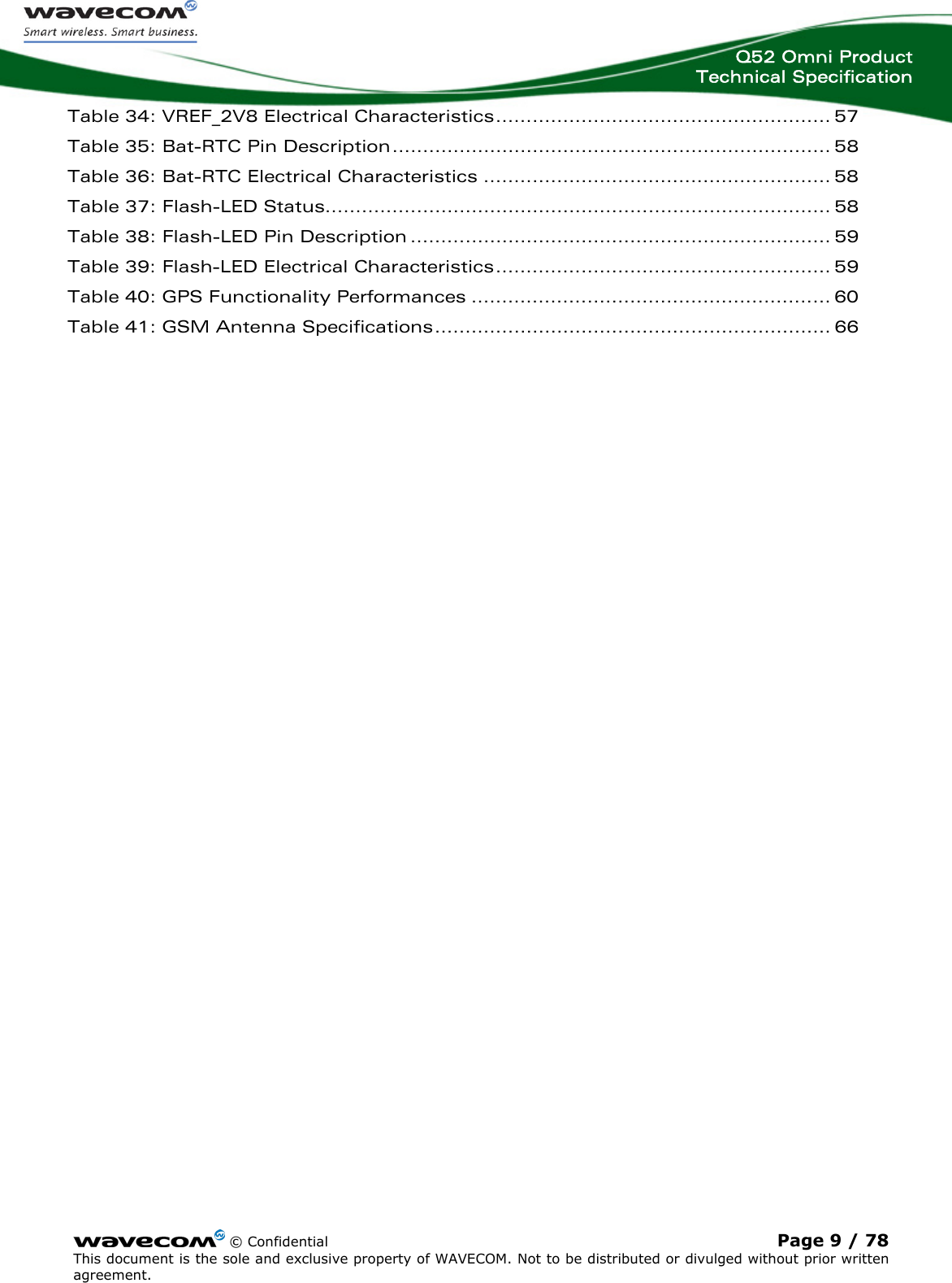
![Q52 Omni Product Technical Specification © Confidential Page 37 / 78 This document is the sole and exclusive property of WAVECOM. Not to be distributed or divulged without prior written agreement. Customer Application( DTE )Q52 Omni( DCE )GNDPWR_EN~CT109-DCD1 / GPIO43~CT108-2-DTR1 / GPIO41~CT125-RI1 / GPIO4212232624GNDDCDDTRRIGND22.8Volt2x 15KCT103-TXD1 / GPIO36CT104-RXD1 / GPIO37~CT105-RTS1 / GPIO38~CT106-CTS1 / GOPI3925283027RxRTSCTSTx Figure 10: Example of full modem V24/CMOS serial link implementation for UART1 It is recommended to add a 15K-ohm pull-up resistor on ~CT125-RI1 and ~CT109-DCD1 to set high level during reset state. The UART1 interface is 2.8 Volt type, but is 3 Volt tolerant. The Q52 Omni UART1 is designed to operate using all the serial interface signals. In particular, it is mandatory to use RTS and CTS for hardware flow control in order to avoid data corruption during transmission. Warning: If you want to activate Power Down mode (Wavecom 32K mode) in your Open AT® application, you need to wire the DTR pin to a GPIO. Please refer to the document [3] AT Command Interface Guide for Open AT® Firmware v7.0 (see the “Appendixes”) for more information on Wavecom 32K mode activation using the Open AT® Software Suite.](https://usermanual.wiki/Sierra-Wireless/Q52OMNI/User-Guide-1038962-Page-38.png)
![Q52 Omni Product Technical Specification 3.6 Auxiliary Serial Link (UART2) 3.6.1 Features The maximum baud rate of UART2 is 921 kbit/s. For peripheral connectivity an auxiliary serial interface (UART2) is available on the system connector only on series without GPS functionality. On Q52 Omni series with GPS functionality GPIO16 and GPIO17 are available. The signals are the follows: • TX data (CT103/TX) • RX data (CT104/RX) • Request To Send (~CT105/RTS) • Clear To Send (~CT106/CTS) The Q52 Omni is designed to operate using all the serial interface signals. In particular, it is mandatory to use RTS and CTS for hardware flow control in order to avoid data corruption during transmission. For the use case with 2-wire serial interface • This case is possible for connected external chip but not recommended (and forbidden for AT command or modem use) • The external chip must be a flow control • CT103/TXD2*, CT104/RXD2* • The signals ~CT105/RTS2*, ~CT106/CTS2* are not used, please configure the AT command (AT+IFC=0,0. Please refer to the document [3] AT Command Interface Guide for Open AT® Firmware v7.0. • The signal ~CT105/RTS2* must be configured at the low level • The other signal and their multiplexed are not available • Please refer to the document [3] AT Command Interface Guide for Open AT® Firmware v7.0 (see the “Appendixes”). Signal Pin number I/O I/O type Reset state Description Multiplexed with TXD2 37 I 1V8 Z Transmit serial data GPIO14 RXD2 39 O 1V8 Z Receive serial data GPIO15 CTS2 38 O 1V8 Z Clear To Send GPIO16 RTS2 40 I 1V8 Z Request To Send GPIO17 Table 16: UART2 Pin Description See Chapter 3.2.3, “Electrical information for digital I/O” for Open drain, 2V8 and 1V8 voltage characteristics and Reset state definitions. © Confidential Page 38 / 78 This document is the sole and exclusive property of WAVECOM. Not to be distributed or divulged without prior written agreement.](https://usermanual.wiki/Sierra-Wireless/Q52OMNI/User-Guide-1038962-Page-39.png)
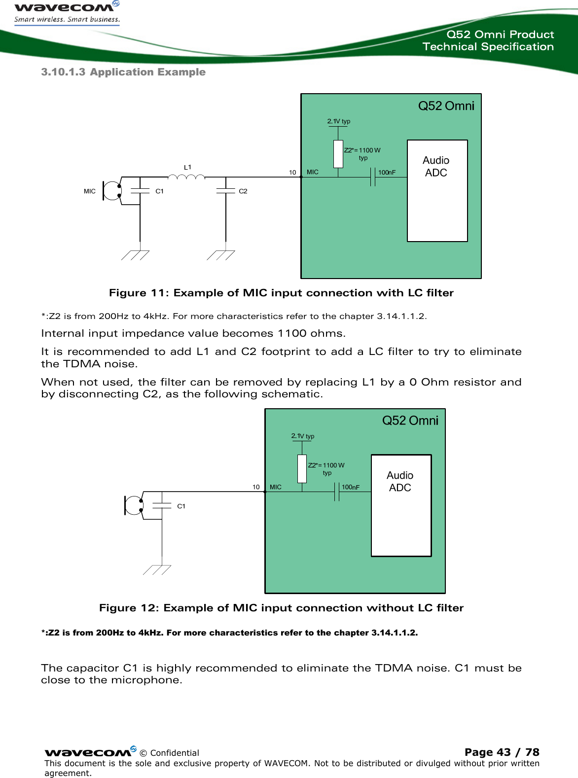
![Q52 Omni Product Technical Specification Recommended components: C1: 12pF to 33pF (depending of the design ,needs to be tuned ) C2: Must be tuned depending of the design. L1: Must be tuned depending of the design. 3.10.2 Speaker Output Characteristics 3.10.2.1 Features The connection is single-ended on SPK. Be sure to have a good ground plane, good filtering and adequate shielding in order to avoid any disturbance on the audio path. Signal Pin number I/O I/O type Description SPK2 7 O Analog Speaker Output Table 24: SPK Pin Description 3.10.2.2 Electrical Characteristics Parameters Min Typ Max Unit Biasing voltage SPK2 1.30 V © Confidential Page 44 / 78 This document is the sole and exclusive property of WAVECOM. Not to be distributed or divulged without prior written agreement. RL=8Ω: AT+VGR=6* - - 2 Vpp Output swing voltage - - RL=32Ω: AT+VGR=6* 2.5 Vpp RL Load resistance 6 8 - Ω IOUT - - 90 mA Output current; peak value; RL=8Ω POUT - - 125 mW RL=8Ω; AT+VGR=6*; RPD Output pull-down resistance at power-down 28 40 52 KΩ VPD Output DC voltage at power-down - - 100 mV Table 25: SPK Electrical Characteristics *The output voltage depends of the output speaker gain set by AT command. Please refer to the document [3] AT Command Interface Guide for Open AT® Firmware v7.0.](https://usermanual.wiki/Sierra-Wireless/Q52OMNI/User-Guide-1038962-Page-45.png)
![Q52 Omni Product Technical Specification The duration of the firmware power-up sequence depends on: • The need to perform a recovery sequence if the power has been lost during a flash memory modification. Other factors have a minor influence • the number of parameters stored in EEPROM by the AT commands received so far • the ageing of the hardware components, especially the flash memory • the temperature conditions The recommended way to de-assert the ~ON/OFF signal is to use either an AT command or WIND indicators: the application has to detect the end of the power-up initialization and de-assert ~ON/OFF afterwards. • Send an “AT” command and wait for the “OK” answer: once the initialization is complete the AT interface answers « OK » to “AT” message*. • Wait for the “+WIND: 3” message: after initialization, the Q52 OMNI /Open AT® Software Suite v2.0, if configured to do so, will return an unsolicited “+WIND: 3” message. The generation of this message is enabled or disabled via an AT command. Note: • Please refer to the document [3] AT Command Interface Guide for Open AT® Firmware v7.00 for more information on these commands. Proceeding thus – by software detection - will always prevent the application from de-asserting the ~ON/OFF signal too early. If WIND indicators are disabled or AT commands unavailable or not used, it is still possible to de-assert ~ON/OFF after a delay long enough (Ton/off-hold) to ensure that the firmware has already completed its power-up initialization. The table below gives the minimum values of Ton/off-hold: Tinitialization minimum values Tinitialization Open AT® Firmware Safe evaluations of the firmware power-up time 6.65 & above 8 s The above figure take the worst cases into account: power-loss recovery operations, slow flash memory operations in high temperature conditions, and so on. But they are safe because they are large enough to ensure that ~ON/OFF is not de-asserted too early. Additional notes: * If the application manages hardware flow control, the AT command can be sent during the initialisation phase. © Confidential Page 52 / 78 This document is the sole and exclusive property of WAVECOM. Not to be distributed or divulged without prior written agreement.](https://usermanual.wiki/Sierra-Wireless/Q52OMNI/User-Guide-1038962-Page-53.png)


![WAVECOM S.A. : 3 esplanade du Foncet - 92442 Issy-les-Moulineaux - France - Tel: +33 1 46 29 08 00 - Fax: +33 1 46 29 08 08Wavecom, Inc: 430 Davis Drive, Suite 300 Research Triangle Park, North Carolina, USA - Tel: +1 919 237 4000 - Fax: +1 919 237 4140WAVECOM Asia-Pacific: Unit 201-207, 2nd Floor, Bio-Informatics Centre No. 2 Science Park West Avenue, Hong Kong Science Park,Shatin, New Territories, Hong Kong (PRC) - Tel: +852-2824 0254 - Fax: +852-2824 0255 [Online contact details, GPS and maps]](https://usermanual.wiki/Sierra-Wireless/Q52OMNI/User-Guide-1038962-Page-80.png)