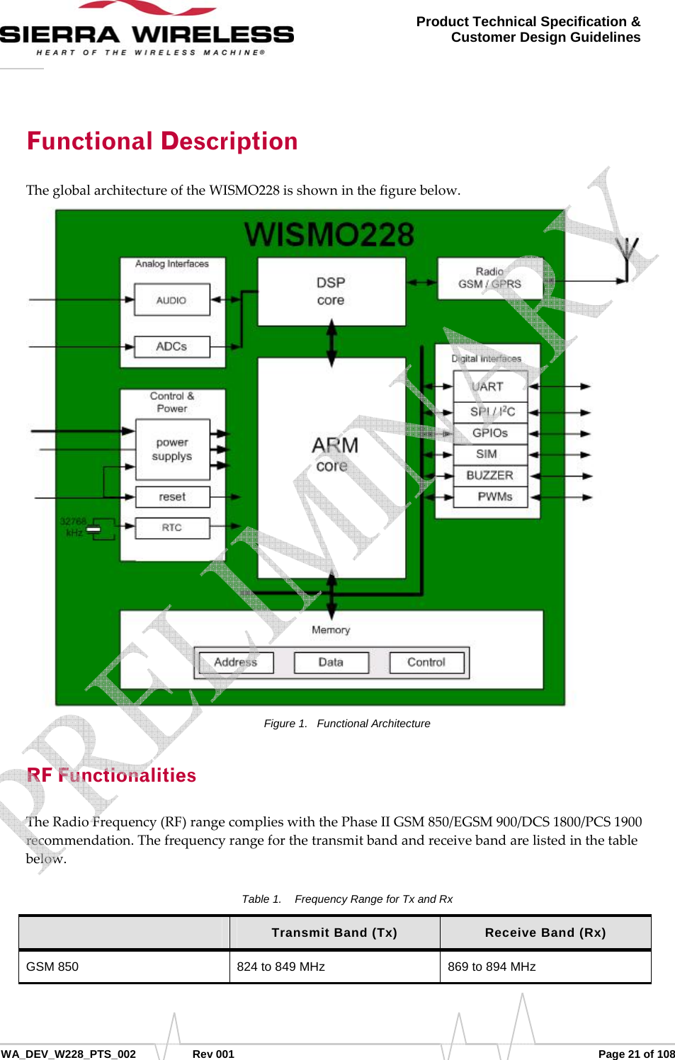
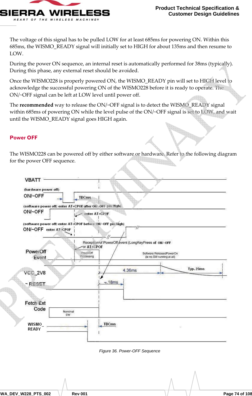
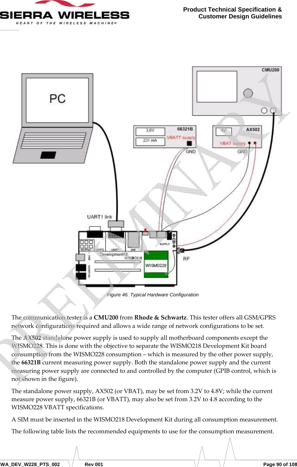
Sierra Wireless WISMO228 MODULE User Manual USERS MANUAL 1

Sierra Wireless Inc. MODULE USERS MANUAL 1

Contents

USERS MANUAL 1

WA_DEV_W228_PTS_002 001 August 26, 2009 WISMO228 WIreless Standard MOdemProduct Technical Specification & Customer Design Guidelines
     WA_DEV_W228_PTS_002 Rev 001  Page 2 of 108 Product Technical Specification & Customer Design Guidelines Important Notice Duetothenatureofwirelesscommunications,transmissionandreceptionofdatacanneverbeguaranteed.Datamaybedelayed,corrupted(i.e.,haveerrors)orbetotallylost.AlthoughsignificantdelaysorlossesofdataarerarewhenwirelessdevicessuchastheSierraWirelessmodemareusedinanormalmannerwithawell‐constructednetwork,theSierraWirelessmodemshouldnotbeusedinsituationswherefailuretotransmitorreceivedatacouldresultindamageofanykindtotheuseroranyotherparty,includingbutnotlimitedtopersonalinjury,death,orlossofproperty.SierraWirelessacceptsnoresponsibilityfordamagesofanykindresultingfromdelaysorerrorsindatatransmittedorreceivedusingtheSierraWirelessmodem,orforfailureoftheSierraWirelessmodemtotransmitorreceivesuchdata.Safety and Hazards DonotoperatetheSierraWirelessmodeminareaswhereblastingisinprogress,whereexplosiveatmospheresmaybepresent,nearmedicalequipment,nearlifesupportequipment,oranyequipmentwhichmaybesusceptibletoanyformofradiointerference.Insuchareas,theSierraWirelessmodemMUST BE POWERED OFF.TheSierraWirelessmodemcantransmitsignalsthatcouldinterferewiththisequipment.DonotoperatetheSierraWirelessmodeminanyaircraft,whethertheaircraftisonthegroundorinflight.Inaircraft,theSierraWirelessmodemMUST BE POWERED OFF.Whenoperating,theSierraWirelessmodemcantransmitsignalsthatcouldinterferewithvariousonboardsystems.Note:   Some airlines may permit the use of cellular phones while the aircraft is on the ground and the door is open. Sierra Wireless modems may be used at this time. ThedriveroroperatorofanyvehicleshouldnotoperatetheSierraWirelessmodemwhileincontrolofavehicle.Doingsowilldetractfromthedriveroroperator’scontrolandoperationofthatvehicle.Insomestatesandprovinces,operatingsuchcommunicationsdeviceswhileincontrolofavehicleisanoffence.
     WA_DEV_W228_PTS_002 Rev 001  Page 3 of 108 Product Technical Specification & Customer Design Guidelines Limitations of Liability Thismanualisprovided“asis”.SierraWirelessmakesnowarrantiesofanykind,eitherexpressedorimplied,includinganyimpliedwarrantiesofmerchantability,fitnessforaparticularpurpose,ornoninfringement.Therecipientofthemanualshallendorseallrisksarisingfromitsuse.TheinformationinthismanualissubjecttochangewithoutnoticeanddoesnotrepresentacommitmentonthepartofSierraWireless.SIERRAWIRELESSANDITSAFFILIATESSPECIFICALLYDISCLAIMLIABILITYFORANYANDALLDIRECT,INDIRECT,SPECIAL,GENERAL,INCIDENTAL,CONSEQUENTIAL,PUNITIVEOREXEMPLARYDAMAGESINCLUDING,BUTNOTLIMITEDTO,LOSSOFPROFITSORREVENUEORANTICIPATEDPROFITSORREVENUEARISINGOUTOFTHEUSEORINABILITYTOUSEANYSIERRAWIRELESSPRODUCT,EVENIFSIERRAWIRELESSAND/ORITSAFFILIATESHASBEENADVISEDOFTHEPOSSIBILITYOFSUCHDAMAGESORTHEYAREFORESEEABLEORFORCLAIMSBYANYTHIRDPARTY.Notwithstandingtheforegoing,innoeventshallSierraWirelessand/oritsaffiliatesaggregateliabilityarisingunderorinconnectionwiththeSierraWirelessproduct,regardlessofthenumberofevents,occurrences,orclaimsgivingrisetoliability,beinexcessofthepricepaidbythepurchaserfortheSierraWirelessproduct.Copyright ©2009SierraWireless.Allrightsreserved.Trademarks AirCard®and“HeartoftheWirelessMachine®”arefiledorregisteredtrademarksofSierraWireless.Watcher®isatrademarkofSierraWireless,registeredintheEuropeanCommunity.SierraWireless,theSierraWirelesslogo,theredwavedesign,andthered-tippedantennaaretrademarksofSierraWireless.,,®,inSIM®,“YOUMAKEIT,WEMAKEITWIRELESS®”,WAVECOM®,WISMO®,WirelessMicroprocessor®,WirelessCPU®,OpenAT®arefiledorregisteredtrademarksofWavecomS.A.inFranceand/orinothercountries.Windows®isaregisteredtrademarkofMicrosoftCorporation.QUALCOMM®isaregisteredtrademarkofQUALCOMMIncorporated.Usedunderlicense.Othertrademarksarethepropertyoftherespectiveowners.
     WA_DEV_W228_PTS_002 Rev 001  Page 4 of 108 Product Technical Specification & Customer Design Guidelines Contact Information Sales Desk: Phone: 1-604-232-1488 Hours:  8:00 AM to 5:00 PM Pacific Time E-mail: sales@sierrawireless.com Post: Sierra Wireless 13811 Wireless Way Richmond, BC Canada                      V6V 3A4 Fax: 1-604-231-1109 Web: www.sierrawireless.com Consultourwebsiteforup-to-dateproductdescriptions,documentation,applicationnotes,firmwareupgrades,troubleshootingtips,andpressreleases:www.sierrawireless.comDocument Update History Rev  Date  History of the evolution 001 August 26, 2009 Creation  
     WA_DEV_W228_PTS_002 Rev 001  Page 5 of 108 Product Technical Specification & Customer Design Guidelines Contents CONTENTS ......................................................................................................................... 5 LISTOFFIGURES .............................................................................................................. 9 LISTOFTABLES .............................................................................................................. 11 1. REFERENCES .............................................................................................................. 13 ReferenceDocuments ............................................................................................................................ 13 WavecomReferenceDocumentation ............................................................................................. 13 ListofAbbreviations ............................................................................................................................. 13 2. GENERALDESCRIPTION ....................................................................................... 19 GeneralInformation .............................................................................................................................. 19 OverallDimensions ......................................................................................................................... 19 EnvironmentandMechanics .......................................................................................................... 19 RoHSDirectiveCompliant .......................................................................................................................  19 CompleteShielding ................................................................................................................................... 19 GSM/GPRSFeatures ........................................................................................................................ 19 Interfaces ........................................................................................................................................... 20 Firmware ........................................................................................................................................... 20 ConnectionInterfaces ...................................................................................................................... 20 FunctionalDescription .......................................................................................................................... 21 RFFunctionalities ............ ......... ........ ......... ........... ......... ......... ........... ......... ........ ......... ........... ......... . 21 BasebandFunctionalities ................................................................................................................. 22 3. INTERFACES ............................................................................................................... 23 GeneralInterfaces .................................................................................................................................. 23 PowerSupply .......................................................................................................................................... 24 PowerSupplyDescription .............................................................................................................. 24 ElectricalCharacteristics ............ ...... ....... ......... ...... ....... ....... ........ ....... ....... ...... ....... ........ ....... ....... ... 25 PinDescription ................................................................................................................................. 25 Application ....................................................................................................................................... 25 PowerConsumption .............................................................................................................................. 27 VariousOperatingModes ............................................................................................................... 27 PowerConsumptionValues ........................................................................................................... 28 ConsumptionWaveformSamples ....... .. .. .. ... .. .... .. ... .. .. .. .. ... .. .. .. .. ..... .. .. .. .. ... .. .. .. .. ... .. .... .. ... .. .. .. .. ... .. . 30 ConnectedModeCurrentWaveform ..................................................................................................... 31 TransferModeClass10CurrentWaveform .......................................................................................... 32 IdleModePage2CurrentWaveform .....................................................................................................  32 IdleModePage9CurrentWaveform .....................................................................................................  33 RecommendationsforLessConsumption ..................................................................................... 33 ElectricalInformationforDigitalI/O ................................................................................................. 34
     WA_DEV_W228_PTS_002 Rev 001  Page 6 of 108 Product Technical Specification & Customer Design Guidelines SPIBusforDebugTraceONLY ......... ....... ...... ....... ....... ........ ....... ....... ...... ......... ....... ...... ....... ...... ........ 35 PinDescription ................................................................................................................................. 35 SPIWaveforms ................................................................................................................................. 35 MainSerialLink(UART) ................ .... ....... .... ..... .... .... ..... .... ....... .... ..... .... .... ..... ...... ..... .... .... ..... .... ..... ... 38 PinDescription ................................................................................................................................. 38 5‐wireSerialInterfaceHardwareDesign ............................................................................................... 39 4‐wireSerialInterfaceHardwareDesign ............................................................................................... 39 2‐wireSerialInterfaceHardwareDesign ............................................................................................... 39 Application ....................................................................................................................................... 40 V24/CMOSPossibleDesign ..................................................................................................................... 41 SIMInterface .......................................................................................................................................... 44 ElectricalCharacteristics ............ ...... ....... ......... ...... ....... ....... ........ ....... ....... ...... ....... ........ ....... ....... ... 44 PinDescription ................................................................................................................................. 45 Application ....................................................................................................................................... 46 SIMSocketConnection .................................................................................................................... 46 GeneralPurposeInput/Output ............................................................................................................ 48 PinDescription ................................................................................................................................. 48 AnalogtoDigitalConverter ................................................................................................................. 49 ElectricalCharacteristics ............ ...... ....... ......... ...... ....... ....... ........ ....... ....... ...... ....... ........ ....... ....... ... 49 PinDescription ................................................................................................................................. 49 AnalogAudioInterface ......................................................................................................................... 50 MicrophoneFeatures ....................................................................................................................... 50 ElectricalCharacteristics ...........................................................................................................................  51 SpeakerFeatures .............................................................................................................................. 52 ElectricalCharacteristics ...........................................................................................................................  52 PinDescription ................................................................................................................................. 53 Application ....................................................................................................................................... 53 Microphone ................................................................................................................................................ 53 SpeakerSPKPadSPKN ............................................................................................................................ 56 DesignRecommendations ........... .................. ................... .................. .................... ................. ........  57 General ........................................................................................................................................................ 57 RecommendedMicrophoneCharacteristics .......................................................................................... 58 RecommendedSpeakerCharacteristics ..................................................................................................  58 RecommendedFilteringComponents .................................................................................................... 58 AudioTrackandPCBLayoutRecommendation .................................................................................. 59 Pulse‐WidthModulators(PWMs) ....................................................................................................... 62 ElectricalCharacteristics ............ ...... ....... ......... ...... ....... ....... ........ ....... ....... ...... ....... ........ ....... ....... ... 62 PinDescription ................................................................................................................................. 62 Application ....................................................................................................................................... 63 BUZZEROutput ..................................................................................................................................... 64 ElectricalCharacteristics ............ ...... ....... ......... ...... ....... ....... ........ ....... ....... ...... ....... ........ ....... ....... ... 64 PinDescription ................................................................................................................................. 65 Application ....................................................................................................................................... 65 LowFilterCalculations .............................................................................................................................  66 RecommendedCharacteristics ................................................................................................................. 66 ON/~OFFSignal ..................................................................................................................................... 68
     WA_DEV_W228_PTS_002 Rev 001  Page 7 of 108 Product Technical Specification & Customer Design Guidelines ElectricalCharacteristics ............ ...... ....... ......... ...... ....... ....... ........ ....... ....... ...... ....... ........ ....... ....... ... 68 PinDescription ................................................................................................................................. 68 Application ....................................................................................................................................... 69 PowerON ................................................................................................................................................... 69 PowerOFF .................................................................................................................................................. 70 WISMO_READYIndication ................. .............. ............. ............... ............. ................ ............. ............ 72 ElectricalCharacteristics ............ ...... ....... ......... ...... ....... ....... ........ ....... ....... ...... ....... ........ ....... ....... ... 72 PinDescription ................................................................................................................................. 72 VCC_2V8Output ................................................................................................................................... 73 ElectricalCharacteristics ............ ...... ....... ......... ...... ....... ....... ........ ....... ....... ...... ....... ........ ....... ....... ... 73 PinDescription ................................................................................................................................. 73 Application ....................................................................................................................................... 73 BAT‐RTC(BackupBattery)................................................................................................................... 74 ElectricalCharacteristics ............ ...... ....... ......... ...... ....... ....... ........ ....... ....... ...... ....... ........ ....... ....... ... 74 PinDescription ................................................................................................................................. 74 Application ....................................................................................................................................... 74 SuperCapacitor ......................................................................................................................................... 75 Non‐RechargeableBattery ........................................................................................................................  75 RechargeableBatteryCell .........................................................................................................................  76 TX_CTRLSignalforTXBurstIndication ........... ............... .................. ............... .................. ..............  77 ElectricalCharacteristics ............ ...... ....... ......... ...... ....... ....... ........ ....... ....... ...... ....... ........ ....... ....... ... 77 PinDescription ................................................................................................................................. 78 Application ....................................................................................................................................... 78 Reset ......................................................................................................................................................... 79 ElectricalCharacteristics ............ ...... ....... ......... ...... ....... ....... ........ ....... ....... ...... ....... ........ ....... ....... ... 79 PinDescription ................................................................................................................................. 80 Application ....................................................................................................................................... 80 RFInterface ............................................................................................................................................. 82 RFConnection .................................................................................................................................. 82 RFPerformances .............................................................................................................................. 83 AntennaSpecifications .................................................................................................................... 83 4. CONSUMPTIONMEASUREMENTPROCEDURE ............................................. 85 HardwareConfiguration ....................................................................................................................... 85 Equipments ....................................................................................................................................... 85 WISMO218DevelopmentKit ......................................................................................................... 87 Socket‐UpBoard .................. ..... .... .... ....... .... ..... .... ..... .... .... ....... .... ..... .... .... ..... .... ....... .... ..... .... .... ..... . 88 SIMCards ......................................................................................................................................... 88 SoftwareConfiguration ......................................................................................................................... 88 WISMO228Configuration ........... ............... ................ ................. ................ ................. ................ ...  88 EquipmentConfiguration ............................................................................................................... 89 Template .................................................................................................................................................. 90 5. TECHNICALSPECIFICATIONS ............................................................................. 93
     WA_DEV_W228_PTS_002 Rev 001  Page 8 of 108 Product Technical Specification & Customer Design Guidelines CastellationPins ........... ......... ......... ......... .......... ......... ......... ........... ......... ........ ......... ........... ......... .......... 93 PinConfiguration .......... ................. ................ ................. ................ ................. ............... ................. 93 PinDescription ................................................................................................................................. 94 RecommendedConnectionWhenNotUsed................................................................................. 95 PCBSpecificationsfortheApplicationBoard ......... ................ ................. ................ ................. ........  96 EnvironmentalSpecifications .............................................................................................................. 97 FunctionStatusClassification ......................................................................................................... 97 ClassA ........................................................................................................................................................ 97 ClassB ......................................................................................................................................................... 97 MechanicalSpecifications .................................................................................................................... 99 PhysicalCharacteristics ................................................................................................................... 99 RecommendedPCBLandingPattern ................. .. ... .. .. .. ..... .. .. .. .. ... .. .. .. .. ... .. .... .. .. ... .. .. .. .. ... .. .. .. ..... .. . 99 WISMO228Dimensions .................................................................................................................. 99 6. RECOMMENDEDPERIPHERALDEVICES ....................................................... 100 GeneralPurposeConnector ................................................................................................................  100 SIMCardReader .................................................................................................................................. 100 Microphone ........................................................................................................................................... 100 Speaker .................................................................................................................................................. 100 AntennaCable ...................................................................................................................................... 101 GSMAntenna ....................................................................................................................................... 101 7. NOISESANDDESIGN ........................................................................................... 102 EMCRecommendations ......................................................................................................................  102 PowerSupply ........................................................................................................................................ 102 Overvoltage ........................................................................................................................................... 102 8. APPENDIX ................................................................................................................. 103 StandardsandRecommendations ..................................................................................................... 103 SafetyRecommendations(forInformationOnly) .......................................................................... 106 RFSafety ......................................................................................................................................... 106 GeneralSafety ....... ......... ........ ........... ......... ......... ......... ........... ......... ........ ......... ........... ......... ....... ... 107 
     WA_DEV_W228_PTS_002 Rev 001  Page 9 of 108 Product Technical Specification & Customer Design Guidelines List of Figures Figure1. FunctionalArchitecture...............................................................................................................21 Figure2. PowerSupplyDuringBurstEmission......................................................................................24 Figure3. RejectFilterDiagram....................................................................................................................25 Figure4. SPITimingDiagram.....................................................................................................................35 Figure5. ExampleofanSPItoUART2InterfaceConversionImplementation.................................36 Figure6. ExampleofanRS‐232LevelShifterImplementationforUART2........................................37 Figure7. ExampleofRS‐232LevelShifterImplementationforUART................................................40 Figure8. ExampleofV24/CMOSSerialLinkImplementationfora2‐wireUART............................41 Figure9. ExampleofV24/CMOSSerialLinkImplementationfora4‐wireUART............................42 Figure10. ExampleofV24/CMOSSerialLinkImplementationfora5‐wireUART............................42 Figure11. ExampleofaFullModemV24/CMOSSerialLinkImplementationforafullUART.......43 Figure12. ExampleofaSIMSocketImplementation...............................................................................46 Figure13. DCEquivalentCircuitofMIC....................................................................................................50 Figure14. ACEquivalentCircuitofMIC....................................................................................................50 Figure15. EquivalentCircuitofSPK............................................................................................................52 Figure16. ExampleofaDifferentialMICConnectionwithanLCFilter..............................................54 Figure17. ExampleofaDifferentialMICConnectionwithoutanLCFilter........................................54 Figure18. ExampleofaSingle‐EndedMICConnectionwithanLCfilter............................................55 Figure19. ExampleofaSingle‐EndedMICConnectionwithoutanLCFilter.....................................56 Figure20. ExampleofaDifferentialSpeakerConnection........................................................................57 Figure21. ExampleofaSingle‐EndedSpeakerConnection....................................................................57 Figure22. CapacitorSolderedinParalleltotheMicrophone..................................................................58 Figure23. AudioTrackDesign.....................................................................................................................60 Figure24. DifferentialAudioConnection...................................................................................................60 Figure25. Single‐EndedAudioConnection...............................................................................................61 Figure26. RelativeTimingforthePWMOutput.......................................................................................62 Figure27. ExampleofanLEDDrivenbythePWM0orPWM1Output...............................................63 Figure28. BUZZEROutput...........................................................................................................................64 Figure29. ExampleofaBUZZERImplementation...................................................................................65 Figure30. ExampleofanLEDDrivenbytheBUZZEROutput..............................................................67 Figure31. ExampleoftheON/~OFFPinConnection...............................................................................69
     WA_DEV_W228_PTS_002 Rev 001  Page 10 of 108 Product Technical Specification & Customer Design Guidelines Figure32. Power‐ONSequence....................................................................................................................69 Figure33. Power‐OFFSequence...................................................................................................................70 Figure34. RTCSuppliedbyaGoldCapacitor...........................................................................................75 Figure35. RTCSuppliedbyaNonRechargeableBattery........................................................................75 Figure36. RTCSuppliedbyaRechargeableBatteryCell.........................................................................76 Figure37. TX_CTRLStateDuringTXBurst...............................................................................................77 Figure38. ExampleofaTXStatusImplementation..................................................................................78 Figure39. ResetTiming..................................................................................................................................79 Figure40. Exampleof~RESETPinConnectionwithaPushButtonConfiguration...........................80 Figure41. Exampleof~RESETPinConnectionwithaTransistorConfiguration...............................80 Figure42. Exampleofa50ΩRFLine...........................................................................................................82 Figure43. TypicalHardwareConfiguration..............................................................................................86 Figure44. WISMO228PinConfiguration....................................................................................................93 Figure45. PCBStructureExamplefortheApplicationBoard.................................................................96 Figure46. WISMO228Dimensions...............................................................................................................99
     WA_DEV_W228_PTS_002 Rev 001  Page 11 of 108 Product Technical Specification & Customer Design Guidelines List of Tables Table1. FrequencyRangeforTxandRx..............................................................................................21 Table2. WISMO228Interfaces................................................................................................................23 Table3. InputPowerSupplyVoltage...................................................................................................25 Table4. PowerSupplyPinDescription................................................................................................25 Table5. WISMO228OperatingModes..................................................................................................27 Table6. WISMO228PowerConsumption............................................................................................29 Table7. Consumption/SoftwareDriverRecommendations.............................................................33 Table8. ElectricalCharacteristicsofDigitalI/Os................................................................................34 Table9. SPIBusPinDescription............................................................................................................35 Table10. MainSerialLinkPinDescription............................................................................................38 Table11. ElectricalCharacteristicsoftheSIMInterface......................................................................44 Table12. SIMInterfacePinDescription..................................................................................................45 Table13. SIMSocketPinDescription......................................................................................................46 Table14. GPIOPinDescriptions..............................................................................................................48 Table15. ElectricalCharacteristicsoftheADCInterface.....................................................................49 Table16. AnalogtoDigitalConverterPinDescription........................................................................49 Table17. ElectricalCharacteristicsofMIC.............................................................................................51 Table18. SpeakerDetails...........................................................................................................................52 Table19. ElectricalCharacteristicsofSPK..............................................................................................52 Table20. AnalogAudioInterfacePinDescription...............................................................................53 Table21. ElectricalCharacteristicsofthePWMInterface...................................................................62 Table22. PWMPinDescription................................................................................................................62 Table23. ElectricalCharacteristicsoftheBUZZERSignal..................................................................64 Table24. BUZZERPinDescription..........................................................................................................65 Table25. ElectricalCharacteristicsoftheON/~OFFSignal.................................................................68 Table26. ON/~OFFSignalPinDescription............................................................................................68 Table27. Power‐ONSequence.................................................................................................................69 Table28. ElectricalCharacteristicsoftheWISMO_READYIndication............................................72 Table29. WISMO_READYIndicationPinDescription........................................................................72 Table30. ElectricalCharacteristicsoftheVCC_2V8Signal.................................................................73
     WA_DEV_W228_PTS_002 Rev 001  Page 12 of 108 Product Technical Specification & Customer Design Guidelines Table31. VCC_2V8PinDescription........................................................................................................73 Table32. ElectricalCharacteristicsoftheBAT‐RTCSignal.................................................................74 Table33. BAT‐RTCPinDescription........................................................................................................74 Table34. TX_CTRLStatus.........................................................................................................................77 Table35. ElectricalCharacteristicsoftheTX_CTRLSignal................................................................77 Table36. TX_CTRLSignalPinDescription............................................................................................78 Table37. ElectricalCharacteristicsoftheResetSignal.........................................................................79 Table38. ResetPinDescription................................................................................................................80 Table39. ResetCommands.......................................................................................................................81 Table40. AntennaSpecifications..............................................................................................................83 Table41. ListofRecommendedEquipments.........................................................................................87 Table42. OperatingModeInformation..................................................................................................89 Table43. WISMO228PowerConsumption............................................................................................90 Table44. WISMO228CastellationPinDescription...............................................................................94 Table45. RecommendedConnectionWhenNotUsed........................................................................95 Table46. OperatingClassTemperatureRange.....................................................................................97 Table47. EnvironmentalClasses..............................................................................................................98
     WA_DEV_W228_PTS_002 Rev 001  Page 13 of 108 Product Technical Specification & Customer Design Guidelines 1. References Reference Documents Severaldocumentsarereferencedthroughoutthisspecification.Formoredetails,pleaseconsultthelistedreferencedocuments.TheWAVECOMdocumentsreferencedhereinareprovidedintheWAVECOMdocumentationpackage;however,thegeneralreferencedocumentswhicharenotWAVECOMownedarenotprovidedinthedocumentationpackage.Wavecom Reference Documentation WISMO218HardwarePresentationReference:WA_DEV_W218_PTS_001WISMO218ATCommandsManualReference:WA_DEV_W218_UGD_003WISMO218DevelopmentKitUserGuideReference:WA_DEV_W218_UGD_004CustomerProcessGuidelineforWISMOSeriesReference:WM_DEV_W218_PTS_001List of Abbreviations Abbreviation  Definition AC Alternative Current ADC  Analog to Digital Converter A/D  Analog to Digital conversion AF Audio-Frequency AGC  Automatic Gain Control AT  ATtention (prefix for modem commands) AUX AUXiliary CAN Controller Area Network
     WA_DEV_W228_PTS_002 Rev 001  Page 14 of 108 Product Technical Specification & Customer Design Guidelines Abbreviation  Definition CB Cell Broadcast CBS Cell Broadcast Service CE - CEP Circular Error Probable CLK CLocK CMOS Complementary Metal Oxide Semiconductor CODEC COder DECoder CPU Central Processing Unit CS Coding Scheme CSD Circuit Switched Data CTS Clear To Send DAC  Digital to Analog Converter DAI Digital Audio Interface dB Decibel DC Direct Current DCD Data Carrier Detect DCE  Data Communication Equipment DCS  Digital Cellular System DR Dynamic Range DSR Data Set Ready DTE Data Terminal Equipment DTR Data Terminal Ready EFR  Enhanced Full Rate E-GSM Extended GSM EMC ElectroMagnetic Compatibility EMI ElectroMagnetic Interference
     WA_DEV_W228_PTS_002 Rev 001  Page 15 of 108 Product Technical Specification & Customer Design Guidelines Abbreviation  Definition EMS  Enhanced Message Service EN ENable ESD ElectroStatic Discharges ETSI European Telecommunications Standards Institute FIFO First In First Out FR Full Rate FTA Full Type Approval GND GrouND GPI General Purpose Input GPC General Purpose Connector GPIO  General Purpose Input Output GPO General Purpose Output GPRS General Packet Radio Service GPS  Global Positioning System GPSI General Purpose Serial Interface GSM  Global System for Mobile communications HR Half Rate Hi Z  High impedance (Z) IC Integrated Circuit IDE Integrated Development Environment IF Intermediate Frequency IMEI  International Mobile Equipment Identification I/O Input / Output LCD Liquid Crystal Display LED  Light Emitting Diode LNA Low Noise Amplifier
     WA_DEV_W228_PTS_002 Rev 001  Page 16 of 108 Product Technical Specification & Customer Design Guidelines Abbreviation  Definition LSB  Less Significant Bit MAX MAXimum MIC MICrophone MIN MINimum MMS  Multimedia Message Service MO Mobile Originated MS Mobile Station MT Mobile Terminated na Not Applicable NF Noise Factor NMEA  National Marine Electronics Association NOM NOMinal NTC Négative Temperature Coefficient PA Power Amplifier Pa  Pascal (for speaker sound pressure measurements) PBCCH  Packet Broadcast Control CHannel PC Personal Computer PCB Printed Circuit Board PCL Power Control Level PCM Pulse Code Modulation PCS  PDA  Personal Digital Assistant PFM Power Frequency Modulation PLL Phase Lock Loop PSM Phase Shift Modulation PWM Pulse Width Modulation
     WA_DEV_W228_PTS_002 Rev 001  Page 17 of 108 Product Technical Specification & Customer Design Guidelines Abbreviation  Definition RAM Random Access Memory RF Radio Frequency RFI Radio Frequency Interference RHCP  Right Hand Circular Polarization RI Ring Indicator RMS Root Mean Square RST ReSeT RTC   Real Time Clock RTCM  Radio Technical Commission for Maritime services RTS Request To Send RX Receive  SCL Serial CLock SDA Serial DAta SIM Subscriber Identification Module SMD Surface Mounted Device/Design SMS Short Message Service SPI Serial Peripheral Interface SPL Sound Pressure Level SPK SPeaKer SW SoftWare PSRAM Pseudo Static RAM TBC To Be Confirmed TDMA Time Division Multiple Access TP Test Point TU  Typical Urban fading profile TUHigh  Typical Urban, High speed fading profile
     WA_DEV_W228_PTS_002 Rev 001  Page 18 of 108 Product Technical Specification & Customer Design Guidelines Abbreviation  Definition TVS Transient Voltage Suppressor TX Transmit TYP TYPical UART Universal Asynchronous Receiver-Transmitter UBX  µ-blox proprietary protocol (NE DOIT PAS APPARAITRE) USB  Universal Serial Bus USSD Unstructured Supplementary Services Data VSWR Voltage Standing Wave Ratio WAP  Wireless Application Protocol 
     WA_DEV_W228_PTS_002 Rev 001  Page 19 of 108 Product Technical Specification & Customer Design Guidelines 2. General Description General Information TheWISMO228isaself‐containedGSM850/EGSM900/DCS1800/PCS1900quad‐bandmodulethatwasspecificallydesignedforM2Msystemsdeployedallovertheworld.Overall Dimensions • Length:25.0mm• Width:25.0mm• Thickness:2.8mm(excludinglabelthickness)• Weight:3.64gEnvironment and Mechanics RoHS Directive Compliant TheWISMO228iscompliantwithRoHSDirective2002/95/ECwhichsetslimitsfortheuseofcertainrestrictedhazardoussubstances.Thisdirectivestatesthat“from1stJuly2006,newelectricalandelectronicequipmentputonthemarketdoesnotcontainlead,mercury,cadmium,hexavalentchromium,polybrominatedbiphenyls(PBB)orpolybrominateddiphenylethers(PBDE)”.Complete Shielding AllelectronicpartsoftheWISMO228arenearly‐completelycoveredinaself‐containedshield.GSM/GPRS Features • 2WattsGSM850radiosectionrunningunder3.6Volts• 2WattsEGSM900radiosectionrunningunder3.6Volts• 1WattDCS1800radiosectionrunningunder3.6Volts• 1WattPCS1900radiosectionrunningunder3.6Volts• HardwareGPRSclass10capable
     WA_DEV_W228_PTS_002 Rev 001  Page 20 of 108 Product Technical Specification & Customer Design Guidelines Interfaces • VBATpowersupply• Digitalsectionrunningunder2.8Volts• 3V/1V8SIMinterface• Powersupplies• Seriallink(UART)• Analogaudio• ADC• SerialbusSPIfordebugtrace• PWM0,1andPWM2forbuzzeroutput• GPIOs• ON/~OFF• TXburstindicator• Modulereadyindicator• ResetFirmware • DrivestheWISMO228viaanATcommandinterfaceoveraserialport• FullGSM/GPRSOperatingSystemstack• RealTimeClockwithcalendarConnection Interfaces TheWISMO228hasa46‐pincastellationformfactorwhichprovides:• OneANTpinforRFin/out• Otherpinsforbasebandsignals
     WA_DEV_W228_PTS_002 Rev 001  Page 21 of 108 Product Technical Specification & Customer Design Guidelines Functional Description TheglobalarchitectureoftheWISMO228isshowninthefigurebelow.Figure 1.  Functional Architecture RF Functionalities TheRadioFrequency(RF)rangecomplieswiththePhaseIIGSM850/EGSM900/DCS1800/PCS1900recommendation.Thefrequencyrangeforthetransmitbandandreceivebandarelistedinthetablebelow.Table 1.  Frequency Range for Tx and Rx  Transmit Band (Tx)  Receive Band (Rx) GSM 850  824 to 849 MHz  869 to 894 MHz
     WA_DEV_W228_PTS_002 Rev 001  Page 22 of 108 Product Technical Specification & Customer Design Guidelines  Transmit Band (Tx)  Receive Band (Rx) E-GSM 900  880 to 915 MHz  925 to 960 MHz DCS 1800  1710 to 1785 MHz  1805 to 1880 MHz PCS 1900  1850 to 1910 MHz  1930 to 1990 MHz  TheRFpartoftheWISMO228isbasedonaspecificdualbandchipwhichincludes:• aDigitallow‐IFreceiver• adual‐bandLNA(LowNoiseAmplifier)• anOffsetPLL(PhaseLockedLoop)transmitter• aFrequencysynthesizer• aDigitallyControlledCrystalOscillator(DCXO)• aTx/RxFEM(Front‐EndModule)forquad‐bandGSM/GPRSBaseband Functionalities TheBasebandiscomposedofanARM9,aDSPandananalogelement(withaudiosignals,I/QsignalsandADC).Thecorepowersupplyis1.2Vandthedigitalpowersupplyis2.8V.
     WA_DEV_W228_PTS_002 Rev 001  Page 23 of 108 Product Technical Specification & Customer Design Guidelines 3. Interfaces General Interfaces TheWISMO228hasa46‐pincastellationconnection,whichprovidesaccesstoallavailableinterfaces.ThefollowingtableenumeratestheavailableinterfacesontheWISMO228.
     WA_DEV_W228_PTS_002 Rev 001  Page 24 of 108 Product Technical Specification & Customer Design Guidelines Table 2.  WISMO228 Interfaces Available Interface  Driven by AT commands
     WA_DEV_W228_PTS_002 Rev 001  Page 25 of 108 Product Technical Specification & Customer Design Guidelines Available Interface  Driven by AT commandsSPI Bus for Debug Trace ONLY TheWISMO228providesoneSPIbusthroughthecastellationpin.Caution:  This interface is only used for monitoring trace for debug purposes. Pin Description ThefollowingtableprovidesthepindescriptionoftheSPIbus.Table 3.  SPI Bus Pin Description Pin #  Signal  I/O  I/O Type  Reset State Description 13  SPI-IO  I/O  2V8  Pull down  SPI Serial input/output 14  SPI-O  O  2V8  Pull down  SPI Serial input 15  SPI-CLK  O  2V8  Pull down  SPI Serial Clock 17  ~SPI-CS  O  2V8  Pull up  SPI Enable 25 SPI-IRQ  I  2V8  Pull down SPI Interrupt AnSPI‐to‐UART2conversioncircuitisrequiredtoconverttheSPItracetoUART2.Also,theSPI‐IRQ(pin25)isrequiredforinterrupt.Again,notethattheSPIinterfaceoftheWISMO228isnotopenforapplicationuseotherthandebugtrace.SPI Waveforms Figure 2.  SPI Timing Diagram 
     WA_DEV_W228_PTS_002 Rev 001  Page 26 of 108 Product Technical Specification & Customer Design Guidelines Available Interface  Driven by AT commandsSIM Interface  Yes Error! Reference source not found. No* Error! Reference source not found. Yes Serial Interface (SPI)  No Analog to Digital Converter  No* Pulse-Width Modulators (PWMs)   Yes ON/~OFF  No PWM2 for Buzzer Output   Yes  Module Ready Indication  No VBAT_RTC (Backup Battery)  No TX Burst Indication Signal  No Error! Reference source not found. No *    These interfaces will have AT command support in future versions.
     WA_DEV_W228_PTS_002 Rev 001  Page 27 of 108 Product Technical Specification & Customer Design Guidelines Power Supply Power Supply Description ThepowersupplyisoneofthekeyelementsinthedesignofaGSMterminal.DuetotheburstemissioninGSM/GPRS,thepowersupplymustbeabletodeliverhighcurrentpeaksinashorttime.Duringthesepeaks,theripple(Uripple)onthesupplyvoltagemustnotexceedacertainlimit.RefertoTable4InputPowerSupplyVoltagefortheinputpowersupplyvoltagevalues.ListedbelowarethecorrespondingradioburstratesforthedifferentGPRSclassesincommunicationmode.• AGSM/GPRSclass2terminalemits577μsradioburstsevery4.615ms.(SeeFigure5PowerSupplyDuringBurstEmission.)• AGPRSclass10terminalemits1154μsradioburstsevery4.615ms.VBATTprovidesforthefollowingfunctions:• DirectlysuppliestheRFcomponentswith3.6V.Itisessentialtokeepaminimumvoltagerippleatthisconnectioninordertoavoidanyphaseerror.• Thepeakcurrent(TBDApeakinGSM/GPRSmode)flowswitharatioof: 1/8ofthetime(around577μsevery4.615msforGSM/GPRSclass2)and 1/4ofthetime(around1154μsevery4.615msforGSM/GPRSclass10)withtherisingtimeataround10μs.• Internallyusedtoprovide,viaseveralregulators,thesupplyrequiredforthebasebandsignals.Figure 5.  Power Supply During Burst Emission
     WA_DEV_W228_PTS_002 Rev 001  Page 28 of 108 Product Technical Specification & Customer Design Guidelines Electrical Characteristics Table 4.  Input Power Supply Voltage  Vmin  Vnom  Vmax  ITYP  Imax  Ripple max (Uripp) VBATT2 3.21 3.6 4.8 TBD TBD TBD 1:    This value has to be guaranteed during the burst (with TBDA Peak in GSM or GPRS mode) 2:   The maximum operating Voltage Stationary Wave Ratio (VSWR) is 1.5:1. Note:   When powering the WISMO228 with a battery, the total impedance (battery + protections + PCB) should be less than 150mΩ. Pin Description Table 5.  Power Supply Pin Description Pin Numbers  Signal 29,30 VBATT 20,22,23,26,28,31 GND Application TherejectfiltercanbeconnectedbetweenVBATTandthesupplysourcesifthesupplysourceisnoisy.Caution:  If the reject filter (C1+L1+C2) is an option, a capacitor (i.e. C2) is mandatory close to the VBATT. Figure 6.  Reject Filter Diagram Thefollowingtableslisttherecommendedcomponentstouseinimplementingtherejectfilter.
     WA_DEV_W228_PTS_002 Rev 001  Page 29 of 108 Product Technical Specification & Customer Design Guidelines C1,C2: 10μF+/‐20%Component  Manufacturer GRM21BR60J106KE19L MURATA CM21X5R106M06AT KYOCERA JMK212BJ106MG-T TAYO YUDEN C2012X5R0J106MT TDK L1: 220nH+/‐5%Component  Manufacturer 0805CS-221XJLC COILCRAFT 0805G221J E  STETCO
     WA_DEV_W228_PTS_002 Rev 001  Page 30 of 108 Product Technical Specification & Customer Design Guidelines Power Consumption ThepowerconsumptionlevelsoftheWISMO228varydependingontheoperatingmodeusedandthefollowingsub‐sectionsdescribethepowerconsumptionvaluesoftheWISMO228whenrunninginvariousoperatingmodesandRFbands.Various Operating Modes RefertothefollowingtableforthelistofavailableoperatingmodesontheWISMO228.Table 6.  WISMO228 Operating Modes Mode  Description OFF Mode  When VBATT power is supplied to the WISMO228 but it has not yet been powered ON. Alarm Mode When alarm clock is set for the WISMO228 with ALL of the following conditions: • before time is up • with AT + CPOF having been entered from a computer that is connected to the WISMO228 • with the ON/~OFF signal being left open (remains at HIGH level) Idle Mode  When the WISMO228 has a location update with a live network but with no GSM/GPRS connection, while the UART interface is in sleep mode. Connected Mode  The WISMO228 has GSM voice codec connection with a live network. Transfer Mode  The WISMO228 has GPRS data transfer connection with a live network. NotethattherearetwodifferentmethodsofenteringsleepmodethroughtheATcommand,AT+PSSLEEP.• AT+PSSLEEP=0 TheentryofsleepmodeiscontrolledbytheleveloftheDTRsignalandthefirmware. TheWISMO228willneverentersleepmodewhentheDTR(viewedfromthemoduleside)isofLOWvoltagelevel.Ontheotherhand,theWISMO228willentersleepmodewhentheDTR(viewedfromthemoduleside)isofHIGHvoltagelevel. TowaketheWISMO228up,itisnecessarytotoggletheDTR(viewedfrommoduleside)fromHIGHtoLOWvoltagelevel. Thismethodshouldbeusediftheapplicationneedstoforbidtheentryofsleepmode.• AT+PSSLEEP=1 Theentryofsleepmodeiscontrolledjustbythefirmware.
     WA_DEV_W228_PTS_002 Rev 001  Page 31 of 108 Product Technical Specification & Customer Design Guidelines  WhentheWISMO228hashadnoactivitiesforacertainperiodoftime,itwillentersleepmodeautomatically,regardlessoftheDTRlevel. AnyASCIIcharacterontheUARTcanwaketheWISMO228up.RefertotheWISMO218ATCommandsManualformoreinformationabouttheAT+PSSLEEPcommand.Power Consumption Values ThreeVBATTvalueswereusedtomeasurethepowerconsumptionoftheWISMO228:VBATTmin(3.2V),VBATTmax(4.8V)andVBATTtyp(3.6V).BoththeaveragecurrentandthemaximumcurrentpeakswerealsomeasuredforallthreeVBATTvalues.ThefollowingconsumptionvalueswereobtainedbyperformingmeasurementsonWISMO228samplesatatemperatureof25°Cwiththeassumptionofa50ΩRFoutput.Note:   Power consumption performance is software related. The results listed below are based on the software version TBD.
     WA_DEV_W228_PTS_002 Rev 001  Page 32 of 108 Product Technical Specification & Customer Design Guidelines Table 7.  WISMO228 Power Consumption WISMO228 Power Consumption Operating Mode  Parameters  IMIN average VBATT=4.8VINOM average VBATT=3.6VIMAX average VBATT=3.2V IMAX peak Unit Off Mode*  TBD  TBD  TBD  TBD  µA Alarm Mode  TBD  TBD  TBD  TBD  µA Idle Mode**  Paging 2 (Rx burst occurrence ~0.5s)  TBD TBD  TBD TBD mA Paging 9 (Rx burst occurrence ~2s)  TBD TBD  TBD TBD mA Connected Mode 850 MHz PCL5 (TX power 33dBm)  TBD TBD  TBD TBD mA PCL19 (TX power 5dBm)  TBD TBD  TBD TBD mA 900 MHz PCL5 (TX power 33dBm)  TBD TBD  TBD TBD mA PCL19 (TX power 5dBm)  TBD TBD  TBD TBD mA 1800 MHz PCL0 (TX power 30dBm)  TBD TBD  TBD TBD mA PCL15 (TX power 0dBm)  TBD TBD  TBD TBD mA 1900 MHz PCL0 (TX power 30dBm)  TBD TBD  TBD TBD mA PCL15 (TX power 0dBm)  TBD TBD  TBD TBD mAGPRS  Transfer Mode class 8 (4Rx/1Tx) 850 MHz Gam.3 (TX power 33dBm)  TBD TBD  TBD TBD mA Gam.17 (TX power 5dBm)  TBD TBD  TBD TBD mA900 MHz Gam.3 (TX power 33dBm)  TBD TBD  TBD TBD mA Gam.17 (TX power 5dBm)  TBD TBD  TBD TBD mA1800 MHz  Gam.3 (TX power 30dBm)  TBD TBD  TBD TBD mA
     WA_DEV_W228_PTS_002 Rev 001  Page 33 of 108 Product Technical Specification & Customer Design Guidelines Gam.18 (TX power 0dBm)  TBD TBD  TBD TBD mA1900 MHz Gam.3 (TX power 30dBm)  TBD TBD  TBD TBD mA Gam.18 (TX power 0dBm)  TBD TBD  TBD TBD mATransfer Mode class 10 (3Rx/2Tx) 850 MHz Gam.3 (TX power 33dBm)  TBD TBD  TBD TBD mA Gam.17 (TX power 5dBm)  TBD TBD  TBD TBD mA900 MHz Gam.3 (TX power 33dBm)  TBD TBD  TBD TBD mA Gam.17 (TX power 5dBm)  TBD TBD  TBD TBD mA1800 MHz Gam.3 (TX power 30dBm)  TBD TBD  TBD TBD mA Gam.18 (TX power 0dBm)  TBD TBD  TBD TBD mA1900 MHz Gam.3 (TX power 30dBm)  TBD TBD  TBD TBD mA Gam.18 (TX power 0dBm)  TBD TBD  TBD TBD mA*    Current consumption in OFF mode is measured with BAT-RTC being left open. **    Idle Mode consumption depends on the SIM card used. Some SIM cards respond faster than others, in which case the longer the response time is, the higher the consumption is. Note:   TX means that the current peak is the RF transmission burst (Tx burst).  RX means that the current peak is the RF reception burst (Rx burst), in GSM mode only (worst case). 4. Refer to section 1
     WA_DEV_W228_PTS_002 Rev 001  Page 34 of 108 Product Technical Specification & Customer Design Guidelines ConsumptionMeasurementProcedureformoreinformationregardingconsumptionmeasurementprocedures.Consumption Waveform Samples TheconsumptionwaveformspresentedbelowhaveatypicalVBATTvoltageof3.6VandareforanEGSM900networkconfiguration.Foursignificantoperatingmodeconsumptionwaveformsareshowninthefollowingsubsections,namely:• ConnectedMode(PCL5:Txpower33dBm)• Transfermode(GPRSclass10,gam.3:Txpower33dBm)• Idlemode(Paging2)• Idlemode(Paging9)Note:   The following diagrams only show the waveform of the current, and not the exact values. Connected Mode Current Waveform TXPEAK
     WA_DEV_W228_PTS_002 Rev 001  Page 35 of 108 Product Technical Specification & Customer Design Guidelines Transfer Mode Class 10 Current Waveform Idle Mode Page 2 Current Waveform RXPEAKTXPEAK
     WA_DEV_W228_PTS_002 Rev 001  Page 36 of 108 Product Technical Specification & Customer Design Guidelines Idle Mode Page 9 Current Waveform Recommendations for Less Consumption Forbetterpowerconsumption,inparticularforthequiescentcurrent,itisrecommendedtodrivetheGPIOsasshowninthetablebelow.Table 8.  Consumption/Software Driver Recommendations Pin #  Signal  I/O  I/O Type  Reset State Recommended SW Driver (Logic Level Output State) 16 GPIO3  I/O 2V8  Pull up  1 19 GPIO5  I/O 2V8  Z**  Input: 0  Output: 1 24 GPIO1  I/O 2V8  Pull up  1  **    When GPIO5 is used as a general purpose output, it is necessary to have an external pull up resistor connecting to a 2.8V source. The resistance value depends on the current drain required by the application side. Note:   GPIO2 is dedicated for WISMO_READY and is not open as a GPIO for customer use.  GPIO4 is dedicated for TX burst indication and is not open as GPIO for customer use. RXPEAK
     WA_DEV_W228_PTS_002 Rev 001  Page 37 of 108 Product Technical Specification & Customer Design Guidelines Electrical Information for Digital I/O ThefollowingtabledescribestheelectricalcharacteristicsofthedigitalI/Os(interfacessuchasGPIO,SPI,etc.)availableontheWISMO228.Table 9.  Electrical Characteristics of Digital I/Os 2.8Volt Type (2V8) Parameter  Conditions  I/O Type  Minimum  Typical  Maximum Internal 2.8V power supply    VCC_2V8  2.7V  2.8V  2.95V Input/Output Pin VIL   CMOS -0.4V* -  0.4V VIH   CMOS 2.4V  -  VCC_2V8 + 0.4V VOL   CMOS -  -  0.1V VOH  CMOS 2.7V - - IOH = 4mA CMOS 2.4V  -  - *    Absolute maximum ratings
     WA_DEV_W228_PTS_002 Rev 001  Page 38 of 108 Product Technical Specification & Customer Design Guidelines SPI Bus for Debug Trace ONLY TheWISMO228providesoneSPIbusthroughthecastellationpin.Caution:  This interface is only used for monitoring trace for debug purposes. Pin Description ThefollowingtableprovidesthepindescriptionoftheSPIbus.Table 10.  SPI Bus Pin Description Pin #  Signal  I/O  I/O Type  Reset State Description 13  SPI-IO  I/O  2V8  Pull down  SPI Serial input/output 14 SPI-O  O  2V8  Pull down SPI Serial input 15 SPI-CLK  O  2V8  Pull down SPI Serial Clock 17 ~SPI-CS  O  2V8  Pull up  SPI Enable 25 SPI-IRQ  I  2V8  Pull down SPI Interrupt AnSPI‐to‐UART2conversioncircuitisrequiredtoconverttheSPItracetoUART2.Also,theSPI‐IRQ(pin25)isrequiredforinterrupt.Again,notethattheSPIinterfaceoftheWISMO228isnotopenforapplicationuseotherthandebugtrace.SPI Waveforms Figure 7.  SPI Timing Diagram 
     WA_DEV_W228_PTS_002 Rev 001  Page 39 of 108 Product Technical Specification & Customer Design Guidelines Figure 8.  Example of an SPI to UART2 Interface Conversion Implementation ThefollowingtableliststherecommendedcomponentstouseinimplementingtheSPItoUART2interface.Component  Description/Details  Manufacturer U103 SC16IS750IPW  NXP Semiconductors X101  3, 6864MHz 86SMX surface mount crystal (971-3131)  Farnell R104, R105  10KΩ  R106  1KΩ  C105 22pF   C106 33pF   C107 100nF   AfterconvertingtheSPIsignaltoaUARTsignal,aUARTtransceivercircuitryisneededtocommunicatethisUARTsignaltotheDTE.
     WA_DEV_W228_PTS_002 Rev 001  Page 40 of 108 Product Technical Specification & Customer Design Guidelines Figure 9.  Example of an RS-232 Level Shifter Implementation for UART2 ThefollowingtableliststherecommendedcomponentstouseinimplementingaUARTtransceivercircuitry.Component  Description/Details  Manufacturer U200 LTC2804IGN-1  LINEAR TECHNOLOGY L200 LQH2M CN100K02L  MURATA J200 096615276119 SUBD9F  HARTING R202 NC   R204  100KΩ  C200 1µF   C201 220nF   C207 1µF   C208 1µF   Note:   It is recommended to make SPI signals accessible for diagnostics by reserving some test points, for example. 
     WA_DEV_W228_PTS_002 Rev 001  Page 41 of 108 Product Technical Specification & Customer Design Guidelines Main Serial Link (UART) Aflexible8‐wireserialinterfaceisavailableontheWISMO228thatcomplieswiththeV24protocolsignaling,butnotwiththeV28(electricalinterface)protocol,duetoits2.8Vinterface.ThesupportedbaudratesoftheUARTare1200,2400,4800,9600,19200,38400,57600and115200Kbits,withautobauding;andthesignalsusedbytheUARTare:• TXdata(CT103/TXD)• RXdata(CT104/RXD)• RequestToSend(~CT105/RTS)• ClearToSend(~CT106/CTS)• DataTerminalReady(~CT108/DTR)• DataSetReady(~CT107/DSR)• DataCarrierDetect(~CT109/DCD)• RingIndicator(~CT125/RI).Pin Description ThefollowingtableprovidesthepindescriptionsoftheUARTinterface.Table 11.  Main Serial Link Pin Description *    According to PC (DTE) view Note:   The rising time and falling time of the reception signals (mainly CT103/TXD) have to be less than 300ns.  The WISMO228 is designed to operate using all the serial interface signals and it is recommended to Pin #  Signal*  I/O  I/O Type  Reset State Description 38 CT103/TXD I  2V8  1  Transmit serial data 39 ~CT105/RTS I  2V8  1  Request To Send 40 CT104/RXD O  2V8  0  Receive serial data 41 ~CT106/CTS O  2V8  0  Clear To Send 42 ~CT107/DSR O  2V8  1  Data Set Ready 43 ~CT109/DCD O  2V8  1  Data Carrier Detect 44 ~CT108/DTR I  2V8  1  Data Terminal Ready 45 ~CT125/RI O  2V8  1  Ring Indicator  GND   GND   Ground
     WA_DEV_W228_PTS_002 Rev 001  Page 42 of 108 Product Technical Specification & Customer Design Guidelines use ~CT105/RTS and ~CT106/CTS for hardware flow control in order to avoid data corruption during transmissions. 5-wire Serial Interface Hardware Design Thesignalsusedinthisinterfacehardwaredesignareasfollows:• CT103/TXD• CT104/RXD• ~CT105/RTS• ~CT106/CTS• ‐CT108/DTRThesignal~CT108/DTRmustbemanagedfollowingtheV24protocolsignalingifidlemodeistobeused.Foradetailedconfiguration,refertoFigure13ExampleofV24/CMOSSerialLinkImplementationfora5‐wireUART.Note:   All signals are specified according to PC (DTE) view. 4-wire Serial Interface Hardware Design Thesignalsusedinthisinterfacehardwaredesignareasfollows:• CT103/TXD• CT104/RXD• ~CT105/RTS• ~CT106/CTSThesignal~CT108/DTRcanbeloopedbackto~CT107/DSRfromboththeWISMO228sideandfromtheDTEside.Foradetailedconfiguration,refertoFigure12ExampleofV24/CMOSSerialLinkImplementationfora4‐wireUART.Note:   All signals are specified according to PC (DTE) view. 2-wire Serial Interface Hardware Design Note:   Although this case is possible for a connected external chip, it is not recommended.  All signals are specified according to PC (DTE) view. Thesignalsusedinthisinterfacehardwaredesignareasfollows:• CT103/TXD
     WA_DEV_W228_PTS_002 Rev 001  Page 43 of 108 Product Technical Specification & Customer Design Guidelines • CT104/RXDSignals~CT105/RTSand~CT106/CTSarenotusedinthisconfiguration.ConfiguretheATcommandAT+IFC=0,0todisabletheflowcontrolfunctionontheWISMO228.RefertotheWISMO218ATCommandsManualformoreinformationaboutconfiguringATcommands.Also,• Thesignal~CT108/DTRcanbeloopedbackto~CT107/DSRfromboththeWISMO228sideandfromtheDTEside.• Thesignal~CT105/RTScanbeloopedbackto~CT106/CTSfromboththeWISMO228sideandfromtheDTEside.• Theflowcontrolmechanismhastobemanagedfromthecustomerside.Foradetailedconfiguration,refertoFigure11ExampleofV24/CMOSSerialLinkImplementationfora2‐wireUART.The loop back connection of ~CT108/DTR to ~CT107/DSR is not allowed when AT+PSSLEEP=0 is used, for which sleep mode entry is ~CT108/DTR level dependent. For more details, refer to the discussion about AT + PSSLEEP = 0 in section 0
     WA_DEV_W228_PTS_002 Rev 001  Page 44 of 108 Product Technical Specification & Customer Design Guidelines Power Consumption.  In order to go to sleep mode properly under this instead. For more details, refer to the discussion about AT + PSSLEEP = 1 in section 0
     WA_DEV_W228_PTS_002 Rev 001  Page 45 of 108 Product Technical Specification & Customer Design Guidelines Note:   Power Consumption. Application ThelevelshiftermustbeaV28electricalsignalcompliantwith2.8V.Figure 10. Example of RS-232 Level Shifter Implementation for UART Note:   The U1 chip also protects the WISMO228 against ESD (air discharge) at 15KV. ThefollowingtableliststherecommendedcomponentstouseinimplementingalevelshifterUART.Component  Description/Details  Manufacturer R1, R2  15KΩ  C1, C2, C3, C4, C5  1µF   C6 100nF   C7 6.8uF TANTAL 10V CP32136 AVX U1 ADM3307EACP  ANALOG DEVICES J1 SUB-D9 female   R1andR2arenecessaryonlyduringtheResetstatetoforcethe~CT125/RIand~CT109/DCDsignalstoHIGHlevel.TheADM3307EACPcanbepoweredbytheVCC_2V8(pin46)oftheWISMO228orbyanexternalregulatorat2.8V.
     WA_DEV_W228_PTS_002 Rev 001  Page 46 of 108 Product Technical Specification & Customer Design Guidelines ItisnotnecessarytouselevelshifterswhentheUARTinterfaceisdirectlyconnectedtoahostprocessor.Refertothefollowingsectionsforstepsonhowtoconnecttheinterfaceusingotherdesignimplementations.V24/CMOS Possible Design Figure 11. Example of V24/CMOS Serial Link Implementation for a 2-wire UART Figure 12. Example of V24/CMOS Serial Link Implementation for a 4-wire UART
     WA_DEV_W228_PTS_002 Rev 001  Page 47 of 108 Product Technical Specification & Customer Design Guidelines Figure 13. Example of V24/CMOS Serial Link Implementation for a 5-wire UART ThedesignsshowninFigure11,Figure12andFigure13arebasicdesigns.BoththeDCDandtheRIcanbeleftopenwhennotused.However,amoreflexibledesigntoaccessthisseriallinkwithallmodemsignalsisshownbelow.Figure 14. Example of a Full Modem V24/CMOS Serial Link Implementation for a full UART Aninternal10KΩpull‐upresistorisconnectedonbothRIandDCDtosetthesignalstoHIGHlevelduringtheResetstate.TheUARTinterfaceisa2.8Vtype,butitis3Vtolerant.Note:   The WISMO228 UART is designed to operate using all the serial interface signals. In particular, it is recommended to use ~CT105/RTS and ~CT106/CTS for hardware flow control in order to avoid data corruption during transmission.
     WA_DEV_W228_PTS_002 Rev 001  Page 48 of 108 Product Technical Specification & Customer Design Guidelines SIM Interface TheSubscriberIdentificationModulecanbedirectlyconnectedtotheWISMO228throughthisdedicatedinterface.Thisinterfacecontrolsboth1.8Vand3VSIMcardsandisfullycompliantwithGSM11.11recommendationsconcerningSIMfunctions.TheSIMusesfoursignals,namely:• SIM‐VCC:SIMpowersupply• ~SIM‐RST:reset• SIM‐CLK:clock• SIM‐IO:I/OportItisrecommendedtoaddTransientVoltageSuppressor(TVS)diodesonthesignalsconnectedtotheSIMsocketinordertopreventanyElectrostaticDischarge.TVSdiodeswithlowcapacitance(lessthan10pF)havetobeconnectedontheSIM‐CLKandSIM‐IOsignalstoavoidanydisturbancefromtherisingandfallingedgeofthesignals.TVSdiodesaremandatoryfortheFullTypeApprovalandtheymustbeplacedasclosetotheSIMsocketaspossible.TherecommendedlowcapacitancediodearraytouseistheDALC208SC6fromSTMicroelectronics.Electrical Characteristics ThefollowingtabledescribestheelectricalcharacteristicsoftheSIMinterface.Table 12.  Electrical Characteristics of the SIM Interface Parameters  Conditions  Minimum  Typical  Maximum  Unit SIM-IO VIH  IIH = ± 20µA  0.7xVSIM -  -  V SIM-IO VIL  IIL = 1mA  -  -  0.4  V ~SIM-RST, SIM-CLK VOH  Source current = 20µA  0.9xVSIM  -  -  V SIM-IO VOH  Source current = 20µA  0.8xVSIM  -  -  V ~SIM-RST, SIM-IO, SIM-CLK  VOL Sink current = -200µA  - - 0.4 V SIM-VCC Output Voltage  SIM-VCC = 2.9V  2.75  2.9  3.0  V
     WA_DEV_W228_PTS_002 Rev 001  Page 49 of 108 Product Technical Specification & Customer Design Guidelines Parameters  Conditions  Minimum  Typical  Maximum  Unit SIM-VCC = 1.8V  1.65  1.8  1.95  V SIM-VCC current full-power mode  -  -  20  mA Sleep mode with 32kHz system clock enabled.  - - 3 mA SIM-CLK  Rise/Fall Time  Loaded with 30pF and ESD protection diode  - 25 50 ns ~SIM-RST, Rise/Fall Time  Loaded with 30pF and ESD protection diode  - 45 - ns SIM-IO Rise/Fall Time Loaded with 30pF and ESD protection diode  - 0.2 1 µs SIM-CLK Frequency  Loaded with 30pF  -  -  3.25  MHz Pin Description ThefollowingtableprovidesthepindescriptionoftheSIMinterface.Table 13.  SIM Interface Pin Description Pin #  Signal  I/O  I/O Type  Reset State  Description  Multiplexed 8  SIM-VCC  O  2V9 / 1V8    SIM Power Supply  No 9 SIM-CLK O 2V9 / 1V8 0  SIM Clock  No 10 SIM-IO I/O 2V9 / 1V8 Pull up  SIM Data  No 11 ~SIM-RST O 2V9 / 1V8 0  SIM Reset  No
     WA_DEV_W228_PTS_002 Rev 001  Page 50 of 108 Product Technical Specification & Customer Design Guidelines Application Figure 15. Example of a SIM Socket Implementation ThefollowingtableliststherecommendedcomponentstouseinimplementingtheSIMsocket.Component  Description/Details  Manufacturer C400 100nF   D400 ESDA6V1SC6  ST D401 DALC208SC6  SGS-THOMSON J400 ITT CANNON CCM03 series (Refer to the SIM Card Reader sub-section of section 1 Error! Not a valid result for table. for more information) CANNON SIM Socket Connection ThefollowingtableprovidesthepindescriptionoftheSIMsocket.Table 14.  SIM Socket Pin Description Pin #  Signal  Description 1 VCC  SIM-VCC 2 RST  ~SIM-RST
     WA_DEV_W228_PTS_002 Rev 001  Page 51 of 108 Product Technical Specification & Customer Design Guidelines Pin #  Signal  Description 3 CLK  SIM-CLK 4 CC4  Not connected 5 GND  GROUND 6 VPP  Not connected 7 I/O  SIM-IO 8 CC8  Not connected Note:   CC4 and CC8 are not connected as the WISMO228 does not support the SIM detect feature.
     WA_DEV_W228_PTS_002 Rev 001  Page 52 of 108 Product Technical Specification & Customer Design Guidelines General Purpose Input/Output TheWISMO228providesuptothreeGeneralPurposeI/Os.TheyareusedtocontrolanyexternaldevicesuchasanLCDoraKeyboardbacklight.TheseGPIOsofferthepossibilitytoreadthepinstatewhatevertheirdirectionmaybe.Pin Description ThefollowingtableprovidesthepindescriptionoftheGPIOs.Table 15.  GPIO Pin Descriptions Pin #  Signal  I/O  I/O Type  Reset State 16 GPIO3  I/O 2V8  Pull up 19 GPIO5  I/O 2V8  Pull down 24 GPIO1  I/O 2V8  Pull up WhenGPIO5isusedasageneralpurposeoutput,itisnecessarytohaveanexternalpullupresistorconnectedtoa2.8Vsource.Theresistancevaluewilldependonthecurrentdrainrequiredbytheapplication.Note:   GPIO2 is dedicated for WISMO_READY and is not open as GPIO for customer use.  GPIO4 is dedicated for TX burst indication and is not open as GPIO for customer use.
     WA_DEV_W228_PTS_002 Rev 001  Page 53 of 108 Product Technical Specification & Customer Design Guidelines Analog to Digital Converter OneAnalogtoDigitalConverterinput,AUX‐ADC0,isprovidedbytheWISMO228forcustomerapplications.Itisa10‐bitresolutionconverter,rangingfromeither0to1Vor0to3V,dependingonthegeneralpurposeinputmode.Electrical Characteristics ThefollowingtabledescribestheelectricalcharacteristicsoftheADCinterface.Table 16.  Electrical Characteristics of the ADC Interface Parameters  Minimum  Typical  Maximum  Unit Resolution - 10 - bits Sampling frequency  -  -  200  kHz Input signal range  1 general purpose input  0  -  1  V 1 general purpose input in div-by-3 mode  0 - 3 V Integral non-linearity (INL)  -2.5  -  +2.5  bit Differential non-linearity (DNL)  -1  -  +3  bit Input impedance input resistance   120  -  -  KΩ input capacitance  -  -  10  pF Pin Description ThefollowingtableprovidesthepindescriptionoftheAnalogtoDigitalConverterinterface.Table 17.  Analog to Digital Converter Pin Description Pin #  Signal  I/O  I/O Type  Description 5 AUX-ADC0 I  Analog A/D converter Caution:  The AUX-ADC0 pin is ESD sensitive and it is a must to add ESD protection to this pin once it is externally accessible. The recommended ESD protection to use is the AVL5M02200 from Amotech.
     WA_DEV_W228_PTS_002 Rev 001  Page 54 of 108 Product Technical Specification & Customer Design Guidelines Analog Audio Interface TheWISMO228supportsonemicrophoneinputandonespeakeroutput.Italsoincludesanechocancellationfeaturewhichallowshandsfreefunction.Insomecases,ESDprotectionmustbeaddedontheaudiointerfacelines.Microphone Features Themicrophone,MIC,canhaveeitherasingle‐endedoradifferentialconnection.However,itisstronglyrecommendedtouseadifferentialconnectioninsteadofasingle‐endedconnectioninordertorejectcommonmodenoiseandTDMAnoise.Whenusingasingle‐endedconnection,besuretohaveaverygoodgroundplane,verygoodfilteringaswellasshieldinginordertoavoidanydisturbanceontheaudiopath.ThegainofMICinputsisinternallyadjustedandcanbetunedusingATcommands.TheMICinterfacealreadyincludessuitablebiasingforanelectretmicrophone.Theelectretmicrophonecanbeconnecteddirectlyontheinputsforeasyconnection.ACcouplingisalsoalreadyembeddedintheWISMO228.Figure 16. DC Equivalent Circuit of MIC Figure 17. AC Equivalent Circuit of MIC
     WA_DEV_W228_PTS_002 Rev 001  Page 55 of 108 Product Technical Specification & Customer Design Guidelines Electrical Characteristics Thefollowingtabledescribestheelectricalcharacteristicsoftheaudiointerface,MIC.Table 18.  Electrical Characteristics of MIC Parameters  Minimum  Typical  Maximum  Unit Internal biasing  DC Characteristics MICP - 2.4 - V MICN without 2.2KΩ to GND  - 2.4 - V MICN with 2.2KΩ to GND  - 1.2 - V Output current        mA R2 - 2.2 - KΩ AC Characteristics 200 Hz<F<4 kHz Z2  MICP (MICN=Open)  2.2  KΩ Z2  MICN (MICP=Open) Z2  MICP (MICN=GND)  2.2  Z2  MICN (MICP=GND) Impedance between MICP and MICN without 2.2KΩ to GND   4.5  Impedance between MICP and MICN with 2.2KΩ to GND   3.2  Maximum working voltage  ( MICP-MICN) (THD 10%)  AT+VGT*=1  - -  210  mVpp Maximum rating voltage (MICP or MICN)    -0.5  -  4.4  V *    The input voltage depends on the input micro gain set by the AT command. Refer to the WISMO218 AT Commands Manual for more information about AT commands. Note:   Because both MICP and MICN are internally biased, it is necessary to use a coupling capacitor to connect an audio signal provided by an active generator. Only a passive microphone can be directly connected to the MICP input.
     WA_DEV_W228_PTS_002 Rev 001  Page 56 of 108 Product Technical Specification & Customer Design Guidelines Speaker Features Thespeaker,SPK,caneitherhaveasingle‐endedoradifferentialconnection.However,itisstronglyrecommendedtouseadifferentialconnectioninsteadofasingle‐endedconnectioninordertorejectcommonmodenoiseandTDMAnoise.Moreover,inasingle‐endedconnection,half(½)ofthepowerislost.Figure 18. Equivalent Circuit of SPK Table 19.  Speaker Details Parameters  Typical  Unit  Connection Z (SPKP, SPKN)  16 or 32  Ω Differential Z (SPKP, SPKN)  8  Ω Single-ended Ifasingle‐endedconnectionisused,onlySPKPhastobeconnected.Theresultisamaximaloutputpowerdividedby2.Also,whenusingasingle‐endedconnection,besuretohaveaverygoodgroundplane,verygoodfilteringaswellasshieldinginordertoavoidanydisturbanceontheaudiopath.Electrical Characteristics Thefollowingtabledescribestheelectricalcharacteristicsofthemicrophoneinterface,MIC.NotethatthemaximumvaluesspecifiedinthefollowingtableareavailablewiththemaximumpoweroutputconfigurationvaluessetbyanATcommand;butusingthetypicalvaluesisrecommended.Table 20.  Electrical Characteristics of SPK Parameters  Minimum  Typical  Maximum  Unit Biasing voltage  SPKP and SPKN  -  1.4  -  V Output swing  RL=8Ω: AT+VGR=6*; single ended  - - 1 Vpp
     WA_DEV_W228_PTS_002 Rev 001  Page 57 of 108 Product Technical Specification & Customer Design Guidelines Parameters  Minimum  Typical  Maximum  Unit voltage  RL=8Ω: AT+VGR=6*; differential  - - 2 Vpp RL=16Ω or 32Ω: AT+VGR=6*; single ended  - - 1.1 Vpp RL=16Ω or 32Ω: AT+VGR=6*; differential  - - 2.2 Vpp RL Load resistance  6 8 - Ω IOUT  Output current; peak value; RL=8Ω - - 90 mA POUT  RL=8Ω; AT+VGR=10*;  - - 65 mW *    The output voltage depends on the output speaker gain set by the AT command. Refer to the WISMO218 AT Commands Manual for more information about configuring AT commands. Pin Description Thefollowingtableprovidesthepindescriptionoftheanalogaudiointerface.Table 21.  Analog Audio Interface Pin Description Pin #   Signal  I/O  I/O Type  Description 1 SPKP  O Analog Speaker positive output 2 SPKN  O Analog Speaker negative output 3 MICP  I  Analog Microphone positive input 4 MICN  I  Analog Microphone negative input Application Microphone Thefollowingsub‐sectionsdescribethedifferentmicrophoneconfigurationexamples.Differential Connection WhenadifferentialconnectionofMICisused,itisnecessarytoadda2.2KΩresistorfromMICNtoGNDinordertohaveaproperbiasofthemicrophone.
     WA_DEV_W228_PTS_002 Rev 001  Page 58 of 108 Product Technical Specification & Customer Design Guidelines Figure 19. Example of a Differential MIC Connection with an LC Filter AudioqualitycanbeverygoodwithoutL1,L2,C2,C3andC4dependingonthedesign.ButifthereisEMIperturbation,thisfiltercanreducetheTDMAnoise.Thisfilter(L1,L2,C2,C3andC4)isnotmandatory,andifnotused,thecapacitormustberemovedandthecoilreplacedbya0Ωresistorasshowninthefollowingschematic.Figure 20. Example of a Differential MIC Connection without an LC Filter ThecapacitorC1ishighlyrecommendedtoeliminateTDMAnoiseandmustbeclosetothemicrophone.ThefollowingtableliststherecommendedcomponentstouseinimplementingadifferentialMICconnectionwithoutanLCfilter.
     WA_DEV_W228_PTS_002 Rev 001  Page 59 of 108 Product Technical Specification & Customer Design Guidelines Component  Description/Details  Notes C1  12pF to 33pF  needs to be tuned depending on the design C2, C3, C4  47pF  needs to be tuned depending on the design L1, L2  100nH  needs to be tuned depending on the design Single-Ended Connection Whensingle‐endedconnectionisusedforMIC,MICNisjustleftopen.Figure 21. Example of a Single-Ended MIC Connection with an LC filter Note:   Z2 is from 200Hz to 4kHz. For more details, refer to Table 18 Electrical Characteristics of MIC. Whenusingasingle‐endedconnection,bearinmindthat:• Theinternalinputimpedancevaluebecomes1100Ω,duetotheconnectionoftheotherendtoground.• ThesingleendeddesignisverysensitivetoTDMAnoise.• AverygoodgroundingontheMICisamustinordertoensuregoodaudioperformanceagainstTDMA.Also,specialcareonthePCBlayoutmustbetaken.• ItisrecommendedtoaddL1andC2footprintsasanLCfiltertotrytoeliminateTDMAnoise.• Whennotused,thefiltercanberemovedbyreplacingL1witha0ΩresistorandbydisconnectingC2,asshowninthefollowingschematic.
     WA_DEV_W228_PTS_002 Rev 001  Page 60 of 108 Product Technical Specification & Customer Design Guidelines Figure 22. Example of a Single-Ended MIC Connection without an LC Filter Note:   *Z2 is from 200Hz to 4kHz. For more details, refer to Table 18 Electrical Characteristics of MIC. ThecapacitorC1ishighlyrecommendedtoeliminateTDMAnoiseandmustbeclosetothemicrophone.Thefollowingtableliststherecommendedcomponentstouseinimplementingasingle‐endedMICconnectionwithoutanLCfilter.Component  Description/Details  Notes C1  12pF to 33pF  needs to be tuned depending on the design C2    needs to be tuned depending on the design L1    needs to be tuned depending on the design Speaker SPKP ad SPKN Differential Connection Inadifferentialconnection,simplyconnectbothSPKPandSPKNtothespeaker.
     WA_DEV_W228_PTS_002 Rev 001  Page 61 of 108 Product Technical Specification & Customer Design Guidelines  SPKP SPKN Figure 23. Example of a Differential Speaker Connection Single-Ended Connection Inasingle‐endedconnection,SPKNcanbeleftopen.Refertothefollowingdiagramforatypicalsingle‐endedimplementation.Figure 24. Example of a Single-Ended Speaker Connection Note:   4.7µF < C1 < 47 µF (Depending on speaker characteristics and output power.) Whenusingasingle‐endedconnection,bearinmindthat:• Usingasingle‐endedconnectionincludeslosingoutputpower(‐6dB)ascomparedtoadifferentialconnection.• TheconnectionbetweentheWISMO228pinsandthespeakermustbedesignedtokeeptheserialimpedancelowerthan1.5Ω.Design Recommendations General Whenbothspeakerandmicrophoneareexposedtotheexternalenvironment,itisrecommendedtoaddESDprotectionasclosetothespeakerormicrophoneaspossible,connectedbetweentheaudiolinesandagoodground.Whenusingthesingle‐endedconnectionofMICP,ensuretohaveagoodgroundplane,goodfilteringaswellasshielding,inordertoavoidanydisturbanceontheaudiopath.Itisalsoimportanttoselectanappropriatemicrophone,speakerandfilteringcomponentstoavoidTDMAnoise.
     WA_DEV_W228_PTS_002 Rev 001  Page 62 of 108 Product Technical Specification & Customer Design Guidelines Recommended Microphone Characteristics • Theimpedanceofthemicrophonehastobearound2KΩ• Sensitivityisfrom‐40dBto‐50dB• SNR>50dB• FrequencyresponseiscompatiblewithGSMspecificationsTosuppressTDMAnoise,itishighlyrecommendedtousemicrophoneswithtwointernaldecouplingcapacitors:• CM1=56pF(0402package)fortheTDMAnoisecomingfromthedemodulationoftheGSM850/EGSM900frequencysignals• CM2=15pF(0402package)fortheTDMAnoisecomingfromthedemodulationoftheDCS1800/PCS1900frequencysignalsThecapacitorshavetobesolderedinparalleltothemicrophoneasshowninthefigurebelow. CM Figure 25. Capacitor Soldered in Parallel to the Microphone Recommended Speaker Characteristics • Typeofspeakers:Electro‐magnetic/10mW• Impedance:8Ωforhands‐free• Impedance:32Ωforheadskit• Sensitivity:110dBSPLmin• ReceiverfrequencyresponseiscompatiblewithGSMspecifications.Recommended Filtering Components WhendesigningaGSMapplication,itisimportanttoselecttherightaudiofilteringcomponents.Thestrongestnoise,calledTDMA,ismainlyduetothedemodulationoftheGSM850,EGSM900,DCS1800andPCS1900signals,whereaburstisproducedevery4.615ms;andthefrequencyoftheTDMAsignalisequalto216.7Hzplusharmonics.TDMAnoisecanbesuppressedbyfilteringtheRFsignalusingtheappropriatedecouplingcomponents.
     WA_DEV_W228_PTS_002 Rev 001  Page 63 of 108 Product Technical Specification & Customer Design Guidelines Thetypesoffilteringcomponentsare:• RFdecouplinginductors• RFdecouplingcapacitorsAgood“ChipS‐Parameter”simulatorisavailablefromMurata.Refertohttp://www.murata.com/products/design_support/mcsil/index.htmlformoredetails.UsingdifferentMuratacomponents,itcanbeseenthatdifferentpackages(withdifferentvaluesandratings)canhavedifferentcouplingeffects.RefertothefollowingtableforexamplesusingdifferentMuratacomponents.Package  0402 Filtered band  GSM900 GSM850/900  DCS/PCS Value  100nH 56pF  15pF Types  Inductor Capacitor  Capacitor Position  Serial Shunt  Shunt Manufacturer  Murata Murata  Murata Rated  150mA 50V  50V Reference  LQG15HSR10J02 or LQG15HNR10J02  GRM1555C1H560JZ01  GRM1555C1H150JZ01 or GRM1555C1H150JB01 Package  0603 Filtered band  GSM900 GSM850/900  DCS/PCS Value  100nH 47pF  10pF Types  Inductor Capacitor  Capacitor Position  Serial Shunt  Shunt Manufacturer  Murata Murata  Murata Rated  300mA 50V  50V Reference  LQG18HNR10J00  GRM1885C1H470JA01 or GRM1885C1H470JB01  GRM1885C1H150JA01 or GQM1885C1H150JB01 Audio Track and PCB Layout Recommendation ToavoidTDMAnoise,itisrecommendedtosurroundtheaudiotrackswithgroundasshowninthefollowingfigure.
     WA_DEV_W228_PTS_002 Rev 001  Page 64 of 108 Product Technical Specification & Customer Design Guidelines Figure 26. Audio Track Design Fordifferentialconnections,itisnecessarytoadda2.2KΩresistorfromMICNtoGNDtohaveaproperbiasofthemicrophone.Figure 27. Differential Audio Connection Forsingle‐endedconnections,thenegativepoleofthemicrophone,MICN,shouldbeconnectedtoGND.Differential Audio line is always in parallel
     WA_DEV_W228_PTS_002 Rev 001  Page 65 of 108 Product Technical Specification & Customer Design Guidelines Figure 28. Single-Ended Audio Connection Caution:  It is a must to avoid digital tracks crossing under and over the audio tracks.   Even when MICP is singled-ended, it is highly recommended to have the MIC ground and the LC filter ground to act as an audio analog ground during the PCB layout. This audio ground, together with the MICP signal, should act as the differential line pair. And this audio ground should only be connected to the WISMO228 module ground as close as possible to the castellation GND pin of the WISMO228.   The same case is applicable to SPKP and SPKN.  Also, the audio interface is ESD sensitive. It is a must to add ESD protection to the interface once it is externally accessible. The recommended ESD protection is the ESDA6VIL from ST.
     WA_DEV_W228_PTS_002 Rev 001  Page 66 of 108 Product Technical Specification & Customer Design Guidelines Pulse-Width Modulators (PWMs) TheWISMO228containstwoPulse‐WidthModulators(PWMs)thatcanbeusedinconjunctionwithanexternaltransistorfordrivingavibrator,orabacklightLED.EachPWMusestwo7‐bitunsignedbinarynumbers:onefortheoutputperiodandoneforthepulsewidthorthedutycycle.TherelativetimingforthePWMoutputisshowninthefigurebelow.Figure 29. Relative Timing for the PWM Output Electrical Characteristics ThefollowingtabledescribestheelectricalcharacteristicsofthePWMinterface.Table 22.  Electrical Characteristics of the PWM Interface Parameters  Conditions  Minimum  Typical  Maximum  Unit VOH High impedance load  2.7  2.85  -  V Load with IoH = 4mA  -  2.4  -  V VOL -  - - 0.1 V IPEAK -  - - 4 mA Frequency -  25.6 - 1083.3 kHz Duty cycle  -  0*  -  100*  % Pin Description ThefollowingtableprovidesthepindescriptionofthePulse‐WidthModulators.Table 23.  PWM Pin Description Pin #  Signal  I/O  I/O Type  Description 35 PWM1  O  2V8  PWM output
     WA_DEV_W228_PTS_002 Rev 001  Page 67 of 108 Product Technical Specification & Customer Design Guidelines Pin #  Signal  I/O  I/O Type  Description 36 PWM0  O  2V8  PWM output Application BoththePWM0andPWM1signalscanbeusedinconjunctionwithanexternaltransistorfordrivingavibrator,orabacklightLED.Figure 30. Example of an LED Driven by the PWM0 or PWM1 Output ThevalueofR607canbeharmonizeddependingontheLED(D605)characteristics.TherecommendeddigitaltransistortouseforT601istheDTC144EEfromROHM.
     WA_DEV_W228_PTS_002 Rev 001  Page 68 of 108 Product Technical Specification & Customer Design Guidelines BUZZER Output TheBUZZERsignalcanbeusedinconjunctionwithanexternaltransistor/MOSFETfordrivingabuzzerinordertogiveamaximumcurrentof100mA(PEAK)andanaverageof40mA,dependingonapplicationrequirement.Itoutputsasquarewaveatthedesiredtonefrequency.Thetonefrequenciesareprogrammableandcanbere‐programmedon‐the‐flytogeneratemonophonicaudioringtonesoralerttones.Thetonelevelcanalsobeadjustedin4dBsteps,ormuted.Figure 31. BUZZER Output Electrical Characteristics ThefollowingtabledescribestheelectricalcharacteristicsoftheBUZZERsignal.Table 24.  Electrical Characteristics of the BUZZER Signal Parameters  Conditions  Minimum  Typical  Maximum  Unit VOH High impedance load  2.7  2.85  -  V Load with IoH = 4mA  -  2.4  -  V IPEAK -  - - 4 mA VOL -  - - 0.1 V Frequency -  200 - 2500 Hz Duty cycle  -  0*  -  100*  % Tone level  4 dB step  -24  -  0  dB *    Be mindful of the maximum frequency and the minimum/maximum duty cycle. There is a limitation to these parameters due to the RC environment. The amplitude modulation becomes less fine when the set limits are reached.
     WA_DEV_W228_PTS_002 Rev 001  Page 69 of 108 Product Technical Specification & Customer Design Guidelines Pin Description ThefollowingtableprovidesthepindescriptionoftheBUZZERsignal.Table 25.  BUZZER Pin Description Pin #  Signal  I/O  I/O Type  Description 34 BUZZER  O  2.8V  Buzzer output Application Themaximumpeakcurrentofthetransistor/MOSFETis100mAandthemaximumaveragecurrentis40mA,whilethepeakcurrentoftheBUZZERpinshouldbelessthan4mA.Atransientvoltagesuppressordiodemustbeaddedasshownbelow.Figure 32. Example of a BUZZER Implementation Where:• R1mustbechoseninordertolimitthecurrentatIPEAKmaxto100mAandmustbeadjustedinrelationtothefrequencyandthedutycycleused.• D1=BAV70T‐7orBAS16(forexample)
     WA_DEV_W228_PTS_002 Rev 001  Page 70 of 108 Product Technical Specification & Customer Design Guidelines • T1=FDN335N(forexample)• R2=0Ω• R3=1MΩNote:   A low filter is recommended at low frequencies. Low Filter Calculations Tocomputeforthecut‐offfrequency,usetheformulaFc=1/(2*Π*Req*C1)where:• Fc=cut‐offfrequency• Req=thetotalresistorsinline• C1=thecapacitivechargeonT1andthegroundBearinmindthat:• FcmustbehigherthanFBUZZ‐OUT• Fcmustbeatleast64*FBUZZ‐OUTNote:   The frequency modulation of the BUZZER signal is 64*FBUZZ-OUT. Recommended Characteristics • Electro‐magnetictype• Impedance:7to30Ω• Sensitivity:90dBSPLmin@10cm• Current:60to90mATheBUZZERoutputcanalsobeusedtodriveanLEDasshowninthefigurebelow.
     WA_DEV_W228_PTS_002 Rev 001  Page 71 of 108 Product Technical Specification & Customer Design Guidelines Figure 33. Example of an LED Driven by the BUZZER Output ThevalueofR607canbeharmonizeddependingontheLED(D605)characteristics.TherecommendeddigitaltransistortouseforT601istheDTC144EEfromROHM.
     WA_DEV_W228_PTS_002 Rev 001  Page 72 of 108 Product Technical Specification & Customer Design Guidelines ON/~OFF Signal TheON/~OFFpinisusedtoswitchONorswitchOFFtheWISMO228.Itisinternallyconnectedtothepermanent3.0VsupplyregulatorinsidetheWISMO228viaapull‐upresistor.OncethereisVBATTsupplytotheWISMO228,this3.0VsupplyregulatorwillbeenabledandsotheON/~OFFsignalisbydefaultatHIGHlevel.ALOWlevelsignalhastobeprovidedontheON/~OFFpintoswitchtheWISMO228ON.Caution:  All external signals must be inactive when the WISMO228 is OFF to avoid any damage when starting and to allow the WISMO228 to start and stop correctly. Electrical Characteristics ThefollowingtabledescribestheelectricalcharacteristicsoftheON/~OFFsignal.Table 26.  Electrical Characteristics of the ON/~OFF Signal Parameter  I/O Type  Minimum  Typical  Maximum  Unit VIH 2V8  2.4 - 3.0 V VIL 2V8  - - 0.4 V Pin Description ThefollowingtableprovidesthepindescriptionoftheON/~OFFsignal.Table 27.  ON/~OFF Signal Pin Description Pin #  Signal  I/O  I/O Type  Description 37 ON/~OFF  I  2V8  WISMO228 Power ON/OFF
     WA_DEV_W228_PTS_002 Rev 001  Page 73 of 108 Product Technical Specification & Customer Design Guidelines Application Figure 34. Example of the ON/~OFF Pin Connection Power ON Figure 35. Power-ON Sequence Table 28.  Power-ON Sequence  Minimum (s)  Typical (s)  Maximum (s) Tready 4 5 7 TheON/~OFFsignallevelisdetectedabout250msafterVBATTisavailable.Note:   This timing might be temperature dependant.
     WA_DEV_W228_PTS_002 Rev 001  Page 74 of 108 Product Technical Specification & Customer Design Guidelines ThevoltageofthissignalhastobepulledLOWforatleast685msforpoweringON.Withinthis685ms,theWISMO_READYsignalwillinitiallysettoHIGHforabout135msandthenresumetoLOW.DuringthepowerONsequence,aninternalresetisautomaticallyperformedfor38ms(typically).Duringthisphase,anyexternalresetshouldbeavoided.OncetheWISMO228isproperlypoweredON,theWISMO_READYpinwillsettoHIGHleveltoacknowledgethesuccessfulpoweringONoftheWISMO228beforeitisreadytooperate.TheON/~OFFsignalcanbeleftatLOWleveluntilpoweroff.TherecommendedwaytoreleasetheON/~OFFsignalistodetecttheWISMO_READYsignalwithin685msofpoweringONwhilethelevelpulseoftheON/~OFFsignalissettoLOW,andwaituntiltheWISMO_READYsignalgoesHIGHagain.Power OFF TheWISMO228canbepoweredoffbyeithersoftwareorhardware.RefertothefollowingdiagramforthepowerOFFsequence.Figure 36. Power-OFF Sequence
     WA_DEV_W228_PTS_002 Rev 001  Page 75 of 108 Product Technical Specification & Customer Design Guidelines Software Power OFF TheATcommandAT+CPOFisusedtopowerOFFtheWISMO228.Note:   If the ON/~OFF pin is maintained at LOW level when AT+CPOF is used, the module cannot be switched OFF. Hardware Power OFF ALOWlevelpulseisappliedontheON/~OFFpinforTBCseconds.AT+CPOFwillthenbeautomaticallysenttotheWISMO228.OncetheWISMO228receivestheAT+CPOFcommand,theWISMO228willbeunregisteredfromthenetwork.TheWISMO_READYpinwillbecomeLOWtoindicatethatATcommandsarenolongeravailablefortheWISMO228.IftheON/~OFFsignalisHIGH,thentheWISMO228willalsobeswitchedOFF.
     WA_DEV_W228_PTS_002 Rev 001  Page 76 of 108 Product Technical Specification & Customer Design Guidelines WISMO_READY Indication ThissignalindicatesthestatusoftheWISMO228afterbeingpoweredON.Notethatthereisaninitialpositivepulseoflessthan200msduringpowerON.RefertoFigure35:Power‐ONSequenceformoreinformationregardingthepowerONsequence.OncetheWISMO228isproperlypoweredON,theWISMO_READYsignalwillsettoHIGHtoacknowledgethesuccessfulpoweringONoftheWISMO228beforeitisreadytooperate.Likewise,thepinwillsettoLOWbeforepoweringOFF.Electrical Characteristics ThefollowingtabledescribestheelectricalcharacteristicsoftheWISMO_READYsignal.Table 29.  Electrical Characteristics of the WISMO_READY Indication Parameters  I/O Type  Minimum  Typical  Maximum  Unit VOH 2V8  2.7 2.8 2.95 V VOL 2V8  - - 0.4 V Pin Description ThefollowingtableprovidesthepindescriptionoftheWISMO_READYsignal.Table 30.  WISMO_READY Indication Pin Description Pin #  Signal  I/O  I/O Type  Description 7 WISMO_READY O 2V8 WISMO228 ready indication
     WA_DEV_W228_PTS_002 Rev 001  Page 77 of 108 Product Technical Specification & Customer Design Guidelines VCC_2V8 Output TheVCC_2V8outputvoltagesupplyisavailablewhentheWISMO228isswitchedONandcanonlybeusedforpull‐upresistor(s)andasareferencesupply.Electrical Characteristics ThefollowingtabledescribestheelectricalcharacteristicsoftheVCC_2V8signal.Table 31.  Electrical Characteristics of the VCC_2V8 Signal Parameters  Minimum  Typical  Maximum  Unit VCC_2V8 Output voltage  2.70  2.80  2.95  V Output Current  Full-power mode  -  -  50  mA Sleep mode  -  -  3  mA Pin Description ThefollowingtableprovidesthepindescriptionoftheVCC_2V8voltagesupply.Table 32.  VCC_2V8 Pin Description Pin #  Signal  I/O  I/O Type  Description 46 VCC_2V8  O  Supply Digital supply Application Thisdigitalpowersupplyismainlyusedto:• Pull‐upsignalssuchasI/Os• SupplythedigitaltransistorsdrivingLEDs• ActasavoltagereferencefortheADCinterfaceAUX‐ADC0
     WA_DEV_W228_PTS_002 Rev 001  Page 78 of 108 Product Technical Specification & Customer Design Guidelines BAT-RTC (Backup Battery) TheBAT‐RTC(backupbattery)pinisusedasaback‐uppowersupplyfortheinternalRealTimeClock(RTC).VBATTprovidesthepowersupplytotheRTCwhenVBATTisswitchedonbutaback‐uppowersupplyisneededtosavethedateandhourwhenitisswitchedoff.IfVBATTisavailable,theback‐upbatterycanbechargedbytheinternal3.0Vpowersupplyregulatorviaa2KΩresistorimplementedinsidetheWISMO228.IftheRTCisnotused,thispincanbeleftopen.Electrical Characteristics ThefollowingtabledescribestheelectricalcharacteristicsoftheBAT‐RTCsignal.Table 33.  Electrical Characteristics of the BAT-RTC Signal Parameters  Minimum  Typical  Maximum  Unit Input voltage  -  3.0  -  V Input current consumption*   -  2.5  -  µA Output voltage  2.82  3.0  3.18  V Max charging current (@VBATT=3.6V)  -  0.6  -  mA *    Provided by an RTC back-up battery when the WISMO228 is off and VBATT = 0V. Pin Description ThefollowingtableprovidesthepindescriptionoftheBAT‐RTCvoltagesupply.Table 34.  BAT-RTC Pin Description Pin #  Signal  I/O  I/O Type  Description 6 BAT-RTC I/O Supply RTC Back-up supply Application Thebackuppowersupplycanbeanyofthefollowing:• Asupercapacitor
     WA_DEV_W228_PTS_002 Rev 001  Page 79 of 108 Product Technical Specification & Customer Design Guidelines • Anonrechargeablebattery• ArechargeablebatterycellSuper Capacitor Figure 37. RTC Supplied by a Gold Capacitor Estimatedsupplytimewitha0.47Fgoldcapacitor:25minutes(minimum).Note:   The maximum voltage of the gold capacitor is 3.9V. Non-Rechargeable Battery Figure 38. RTC Supplied by a Non Rechargeable Battery Thediode,D1,ismandatorytopreventthenonrechargeablebatteryfrombeingdamaged.Estimatedsupplytimewithan85mAhbattery:800hours(minimum).
     WA_DEV_W228_PTS_002 Rev 001  Page 80 of 108 Product Technical Specification & Customer Design Guidelines Rechargeable Battery Cell Figure 39. RTC Supplied by a Rechargeable Battery Cell Estimatedsupplytimewithafullycharged3.4mAhrechargeablebattery:7days(minimum).Caution:  Before battery cell assembly, ensure that the cell voltage is lower than 3.0V to avoid damaging the WISMO228.
     WA_DEV_W228_PTS_002 Rev 001  Page 81 of 108 Product Technical Specification & Customer Design Guidelines TX_CTRL Signal for TX Burst Indication TheTX_CTRLsignalisa2.8VindicationsignalforTXBurstwitha100KΩpull‐upresistorimplementedinsidetheWISMO228module.Table 35.  TX_CTRL Status WISMO228 State  TX_CTRL Status During TX burst  Low No TX  High DuringTXburst,therewillbehighercurrentdrainfromtheVBATTpowersupplywhichcausesavoltagedrop.ThisvoltagedropfromVBATTisagoodindicationofahighcurrentdrainsituationduringTXburst.Figure 40. TX_CTRL State During TX Burst Electrical Characteristics ThefollowingtabledescribestheelectricalcharacteristicsoftheTX_CTRLsignal.Table 36.  Electrical Characteristics of the TX_CTRL Signal Parameters  Conditions  Minimum  Typical  Maximum  Unit VOH   2.6 - 2.95 V VOL   - - 0.4 V Tadvance @500mA  - 18 - µs
     WA_DEV_W228_PTS_002 Rev 001  Page 82 of 108 Product Technical Specification & Customer Design Guidelines Parameters  Conditions  Minimum  Typical  Maximum  Unit @1A - 27 - µs Tdelay   - 11 - µs Pin Description ThefollowingtableprovidesthepindescriptionoftheTX_CTRLsignal.Table 37.  TX_CTRL Signal Pin Description Pin #  Signal  I/O  I/O Type  Reset State Description 18  TX_CTRL  O  2V8  1   TX Burst indication Application TheTXburstindicationsignal,TX_CTRL,canbeusedtodriveanLEDthroughatransistor.ItcanbeagoodvisualindicatorforanyTXactivities.Figure 41. Example of a TX Status Implementation ThevalueofR607canbeharmonizeddependingontheLED(D1)characteristics.
     WA_DEV_W228_PTS_002 Rev 001  Page 83 of 108 Product Technical Specification & Customer Design Guidelines Reset The~RESETpinisahardwareresetandshouldonlybeusedforemergencyresets.Ithasa100KΩinternalpullupresistortoVCC_2V8.Toactivatethe«emergency»resetsequence,the~RESETsignalhastobesettoLOWlevelmanually.Thiscanbedonebyusingapushbutton,forexample.Figure 42. Reset Timing Electrical Characteristics Thefollowingtabledescribestheelectricalcharacteristicsofthe~RESETsignal.Table 38.  Electrical Characteristics of the Reset Signal Parameters  Minimum  Typical  Maximum  Unit Input Impedance ( R )*  -  100K  -  Ω Input Impedance (C)  -  10nF    F Cancellation time (Ta) at power up only  -  38  -  ms VH**  1.57 - - V VIL - 0 1.2 V VIH 1.96 2.8 -- V *    Internal pull up resistance **    VH :  Hysterisis Voltage
     WA_DEV_W228_PTS_002 Rev 001  Page 84 of 108 Product Technical Specification & Customer Design Guidelines Pin Description ThefollowingtableprovidesthepindescriptionoftheRESETsignal.Table 39.  Reset Pin Description Pin #  Signal  I/O  I/O Type  Description 12 ~RESET  100K Pull-up   2V8   WISMO228 Reset Application Ifthe«emergency»resetisused,ithastobedrivenbyeitherapushbuttonoranopencollector/draintransistorasshowninthefiguresbelow.GND123Push button~RESETFigure 43. Example of ~RESET Pin Connection with a Push Button Configuration GND~RESETResetcommand T1 Rohm DTC144EEFigure 44. Example of ~RESET Pin Connection with a Transistor Configuration Anopencollectororopendraintransistorcanalsobeusedtodrivethe~RESETpin(duetotheinternalpull‐upresistorembeddedintotheWISMO228).Ifanopencollectorischosen,therecommendeddigitaltransistortouseforT1istheDTC144EEfromROHM.
     WA_DEV_W228_PTS_002 Rev 001  Page 85 of 108 Product Technical Specification & Customer Design Guidelines Table 40.  Reset Commands Reset Command   ~RESET   Operating Mode 1 0 Reset activated 0 1 Reset inactive Note:   It is recommended to add a varistor (such as the AVL5M02200 from AMOTECH) on the ~RESET pin in order to enhance ESD immunity.
     WA_DEV_W228_PTS_002 Rev 001  Page 86 of 108 Product Technical Specification & Customer Design Guidelines RF Interface TheRFinterfaceallowsthetransmissionofradiofrequency(RF)signalsfromtheWISMO228toanexternalantenna.Thisinterfacehasanominalimpedanceof50ΩandaDCresistanceof0Ω.RF Connection TheRFinput/outputoftheWISMO228isthroughoneofthecastellationpins(Pin21,ANT),withgroundedcastellationpinsatbothsides.Thiscastellationpinmustbeconnectedtoa50ΩRFlineinordertoprotecttheantennalinefromthenoisecomingfrombasebandsignals.Figure 45. Example of a 50Ω RF Line The50ΩRFlineissurroundedbytwogroundplanesinordertoprotecttheantennalinefromnoise.Thelengthofthelineshouldn’tbetoolong(nomorethanafewcentimeters)becauseofRFinsertionloss.Thewidthofthelinemustbecalculatedinordertoensurea50Ωcharacteristicimpedance.Forthissamereason,theembeddedRFlineshouldlikewisebekeptabout1cmawayfromany(noisy)basebandsignalinordertoensureagoodRXsensitivitylevel.Theotherendofthe50ΩRFlinecanbeconnectedtoanRFconnectorortoasolderingpadinordertoconnectanantenna.ItisalsopossibletouseanantennachiportodesignaPCBantennadirectlyontheapplicationboard.TheANTpinoftheWISMO228isESDprotectedforboth±4KVcontactand±8KVairdischarge.Note:   The correct antenna cable and connector should be chosen in order to minimize loss in the frequency bands used for GSM800, EGSM900, DCS1800 and PCS1900.  Castellation pin for ANT 50Ω RF line
     WA_DEV_W228_PTS_002 Rev 001  Page 87 of 108 Product Technical Specification & Customer Design Guidelines 0.5dB can be considered as the maximum value for loss between the WISMO228 and an external connector. RF Performances RFperformancesarecompliantwithETSIrecommendationGSM05.05.ListedbelowarethemainparametersforboththeReceiverandtheTransmitter.ThemainparametersfortheReceiverare:• GSM850/EGSM900ReferenceSensitivity=‐108dBm(typ.)• DCS1800/PCS1900ReferenceSensitivity=‐108dBm(typ.)• Selectivity@200kHz:>+9dBc• Selectivity@400kHz:>+41dBc• Lineardynamicrange:63dB• Co‐channelrejection:>=9dBcThemainparametersfortheTransmitterare:• Maximumoutputpower(EGSM):33dBm+/‐2dBatambienttemperature• Maximumoutputpower(GSM1800):30dBm+/‐2dBatambienttemperature• Minimumoutputpower(EGSM):5dBm+/‐5dBatambienttemperature• Minimumoutputpower(GSM1800):0dBm+/‐5dBatambienttemperatureAntenna Specifications Theoptimumoperatingfrequencydependsontheapplication.Adual‐bandoraquad‐bandantennawillworkinthefollowingfrequencybandsandshouldhavethefollowingcharacteristics.Table 41.  Antenna Specifications Characteristic  WISMO228 GSM 850  E-GSM 900  DCS 1800  PCS 1900 TX Frequency   824 to 849 MHz  880 to 915 MHz  1710 to 1785 MHz  1850 to 1910 MHz RX Frequency   869 to 894 MHz  925 to 960 MHz  1805 to 1880 MHz  1930 to 1990 MHz Impedance  50Ω VSWR  Rx max  1.5 :1 Tx max  1.5 :1
     WA_DEV_W228_PTS_002 Rev 001  Page 88 of 108 Product Technical Specification & Customer Design Guidelines Characteristic  WISMO228 Typical radiated gain  0dBi in one direction at least  Caution:  Both mechanical and electrical antenna adaptations are key issues in the design of a GSM terminal. It is strongly recommended to work with an antenna manufacturer to either develop an antenna adapted to the application or to adapt an existing solution to the application.
     WA_DEV_W228_PTS_002 Rev 001  Page 89 of 108 Product Technical Specification & Customer Design Guidelines 5. Consumption Measurement Procedure ThischapterdescribestheconsumptionmeasurementprocedureusedtoobtaintheWISMO228consumptionspecification.TheWISMO228consumptionspecificationvaluesaremeasuredforalloperatingmodesavailableontheproduct.Hardware Configuration Consumptionresultsarehighlydependentonthehardwareconfigurationusedduringmeasurementandthissectiondescribesthehardwareconfigurationsettingsthatmustbeusedtoobtainoptimumconsumptionmeasurements.ThefollowinghardwareconfigurationincludesboththemeasurementequipmentandtheWISMO228withitssocket‐upboardontheWISMO218developmentkit.Equipments Fourdevicesareusedtoperformconsumptionmeasurement:• Acommunicationtester• Acurrentmeasuringpowersupply• Astandalonepowersupply• Acomputer,tocontroltheWISMO228andsavemeasurementdata
     WA_DEV_W228_PTS_002 Rev 001  Page 90 of 108 Product Technical Specification & Customer Design Guidelines Figure 46. Typical Hardware Configuration ThecommunicationtesterisaCMU200fromRhode&Schwartz.ThistesteroffersallGSM/GPRSnetworkconfigurationsrequiredandallowsawiderangeofnetworkconfigurationstobeset.TheAX502standalonepowersupplyisusedtosupplyallmotherboardcomponentsexcepttheWISMO228.ThisisdonewiththeobjectivetoseparatetheWISMO218DevelopmentKitboardconsumptionfromtheWISMO228consumption–whichismeasuredbytheotherpowersupply,the66321Bcurrentmeasuringpowersupply.Boththestandalonepowersupplyandthecurrentmeasuringpowersupplyareconnectedtoandcontrolledbythecomputer(GPIBcontrol,whichisnotshowninthefigure).Thestandalonepowersupply,AX502(orVBAT),maybesetfrom3.2Vto4.8V;whilethecurrentmeasurepowersupply,66321B(orVBATT),mayalsobesetfrom3.2Vto4.8accordingtotheWISMO228VBATTspecifications.ASIMmustbeinsertedintheWISMO218DevelopmentKitduringallconsumptionmeasurement.Thefollowingtableliststherecommendedequipmentstousefortheconsumptionmeasurement.
     WA_DEV_W228_PTS_002 Rev 001  Page 91 of 108 Product Technical Specification & Customer Design Guidelines Table 42.  List of Recommended Equipments Device  Manufacturer  Reference  Notes Communication Tester  Rhode & Schwartz  CMU 200  Quad Band GSM/DCS/GPRS Current measuring power supply  Agilent 66321B Used for VBATT (supplies the WISMO228) Stand alone power supply  Metrix AX502 Used for VBAT (supplies the WISMO218 development kit board) WISMO218 Development Kit TheWISMO218DevelopmentKitisusedasabasisfortheWISMO228measurementviaanadaptorboardandisusedtoperformconsumptionmeasurementusingseveralsettings.RefertotheWISMO218DevelopmentKitUserGuideandtheWISMO218HardwarePresentationformoreinformationaboutthesesettings.Note:   The WISMO218 Development Kit can be replaced by WMP100 Development Kit once a suitable socket-up board is available. TheWISMO218DevelopmentKitboardispoweredbythestandalonepowersupplyatVBAT;whiletheWISMO228ispoweredbythecurrentmeasuringpowersupplyatVBATT.ItisforthisreasonthatthelinkbetweenVBATTandVBAT(J605)mustbeopened(byremovingthesolderatthetopoftheboardintheSUPPLYarea).Notethefollowinginformationregardingbothpowersupplies.• VBATTispoweredbythecurrentmeasuringpowersupply(66321B)• VBATispoweredbythestandalonepowersupply(AX502)throughTP602Alsotakenoteofthefollowingadditionalconfiguration/settings:• TheR600resistorandtheD603andD604diodes(aroundtheBAT‐TEMPconnector)mustberemoved.• TheUART2linkisnotused;therefore,J201,J202,J203,J204mustbeopened(byremovingthesolder).• The“FLASH‐LED”mustbenotused,soJ602mustbeopened(byremovingthesolder).• TheUSBlinkisnotused;therefore,J301,J302,J303,J304,J305mustbeopened(byremovingthesolder).• Audioisnotused;therefore,J702,J703,J704,J705,J605mustbeopened(byremovingthesolder).• ThereisnoSIMdetectfeatureontheWISMO228;therefore,J403mustbeopened(byremovingthesoldered).• Chargingisnotused;therefore,R602mustberemoved.• C600andR607mustberemovedtoavoidunexpectedcurrentconsumption.• Theswitch,BOOT(aroundthe“CONFIG”area),mustbesettotheOFFposition.
     WA_DEV_W228_PTS_002 Rev 001  Page 92 of 108 Product Technical Specification & Customer Design Guidelines ThegoalofthesettingslistedaboveistoeliminateallbiascurrentfromVBATTandtosupplytheentireboard(excepttheWISMO228)usingonlyVBAT.Socket-Up Board Anadaptorboard,theWISMO218Socket‐UpBoard(WM0801706‐020‐20),isusedtoconnecttheWISMO228toworkontheWISMO218DevelopmentKit.Onthissocket‐upboard,thesolderingpointsofJ203,J204,JP101,JP102,JP103,JP104,JP105,JP106andJP107mustbeopened.SIM Cards Consumptionmeasurementmaybeperformedwitheither3‐Voltor1.8‐VoltSIMcards.However,allspecifiedconsumptionvaluesarefora3‐VoltSIMcard.Caution:  The SIM card’s voltage is supplied by the WISMO228’s power supply. Consumption measurement results may vary depending on the SIM card used. Software Configuration Thissectiondiscussesthesoftwareconfigurationfortheequipment(s)usedandtheWISMO228settings.WISMO228 Configuration TheWISMO228softwareconfigurationissimplyperformedbyselectingtheoperatingmodetouseinperformingthemeasurement.AdescriptionoftheoperatingmodesandtheproceduresusedtochangetheoperatingmodearegivenintheappendixofWISMO218ATCommandsManual.TheavailableoperatingmodesintheWISMO228areasfollows:• OFFMode• AlarmMode• IdleMode• ConnectedMode• TransferModeclass8(4Rx/1Tx)(inGPRSmode)• TransferModeclass10(3Rx/2Tx)(inGPRSmode)
     WA_DEV_W228_PTS_002 Rev 001  Page 93 of 108 Product Technical Specification & Customer Design Guidelines Equipment Configuration ThecommunicationtesterissetaccordingtotheWISMO228operatingmode.Pagingduringidlemodes,TXburstpower,RFbandandGSM/DCS/GPRSmaybeselectedonthecommunicationtester.Refertothefollowingtableforthenetworkanalyzerconfigurationaccordingtooperatingmode.Table 43.  Operating Mode Information Operating Mode  Communication Tester Configuration OFF Mode  N/A Alarm Mode  N/A  Idle Mode Paging 2 (Rx burst occurrence ~0,5s) Paging 9 (Rx burst occurrence ~2s) Connected Mode 850 MHz PCL5 (TX power 33dBm) PCL19 (TX power 5dBm) 900 MHz PCL5 (TX power 33dBm) PCL19 (TX power 5dBm) 1800MHz PCL0 (TX power 30dBm) PCL15 (TX power 0dBm) 1900 MHz PCL0 (TX power 30dBm) PCL15 (TX power 0dBm) GPRS Transfer Mode class 8 (4Rx/1Tx) 850 MHz Gam.3 (TX power 33dBm) Gam.17 (TX power 5dBm) 900 MHz Gam.3 (TX power 33dBm) Gam.17 (TX power 5dBm) 1800MHz Gam.3 (TX power 30dBm) Gam.18 (TX power 0dBm) 1900 MHz Gam.3 (TX power 30dBm) Gam.18 (TX power 0dBm) Transfer Mode class 10  850 MHz  Gam.3 (TX power 33dBm)
     WA_DEV_W228_PTS_002 Rev 001  Page 94 of 108 Product Technical Specification & Customer Design Guidelines Operating Mode  Communication Tester Configuration (3Rx/2Tx)  Gam.17 (TX power 5dBm) 900 MHz Gam.3 (TX power 33dBm) Gam.17 (TX power 5dBm) 1800MHz Gam.3 (TX power 30dBm) Gam.18 (TX power 0dBm) 1900 MHz Gam.3 (TX power 30dBm) Gam.18 (TX power 0dBm) Template Thistemplatemaybeusedforconsumptionmeasurementforallmodesandconfigurationsavailable.NotethatthreeVBATTvoltagesareusedtomeasureconsumption,namely:VBATTmin(3.2V),VBATTtyp(3.6V)andVBATTmax(4.8V).Theminimum/maximumRFtransmissionpowerconfigurationsarealsosetandmeasured.Table 44.  WISMO228 Power Consumption WISMO228 Power Consumption Operating Mode  Parameters  IMIN average VBATT=4.8VINOM average VBATT=3.6VIMAX average VBATT=3.2V IMAX peak Unit Off Mode*          µA Alarm Mode          µA Idle Mode TBD     mA Paging 9 (Rx burst occurrence ~2s)       mA Connected Mode 850 MHz PCL5 (TX power 33dBm)       mA PCL19 (TX power 5dBm)       mA 900 MHz  PCL5 (TX power 33dBm)       mA
     WA_DEV_W228_PTS_002 Rev 001  Page 95 of 108 Product Technical Specification & Customer Design Guidelines PCL19 (TX power 5dBm)       mA 1800 MHz PCL0 (TX power 30dBm)       mA PCL15 (TX power 0dBm)       mA 1900 MHz PCL0 (TX power 30dBm)       mA PCL15 (TX power 0dBm)       mAGPRS Transfer Mode class 8 (4Rx/1Tx) 850 MHz Gam.3 (TX power 33dBm)       mA Gam.17 (TX power 5dBm)       mA900 MHz Gam.3 (TX power 33dBm)       mA Gam.17 (TX power 5dBm)       mA1800 MHz Gam.3 (TX power 30dBm)       mA Gam.18 (TX power 0dBm)       mA1900 MHz Gam.3 (TX power 30dBm)       mA Gam.18 (TX power 0dBm)       mATransfer Mode class 10 (3Rx/2Tx) 850 MHz Gam.3 (TX power 33dBm)       mA Gam.17 (TX power 5dBm)       mA900 MHz Gam.3 (TX power 33dBm)       mA Gam.17 (TX power 5dBm)       mA1800 MHz Gam.3 (TX power 30dBm)       mA Gam.18 (TX power 0dBm)       mA
     WA_DEV_W228_PTS_002 Rev 001  Page 96 of 108 Product Technical Specification & Customer Design Guidelines 1900 MHz Gam.3 (TX power 30dBm)       mA Gam.18 (TX power 0dBm)       mA*    Current consumption in OFF mode is measured with BAT-RTC being left open.
     WA_DEV_W228_PTS_002 Rev 001  Page 97 of 108 Product Technical Specification & Customer Design Guidelines 6. Technical Specifications Castellation Pins Pin Configuration Figure 47. WISMO228 Pin Configuration 
     WA_DEV_W228_PTS_002 Rev 001  Page 98 of 108 Product Technical Specification & Customer Design Guidelines Pin Description Table 45.  WISMO228 Castellation Pin Description Pin #  Signal  Description  I/O  Pin #  Signal  Description  I/O 1  SPKP  Speaker output positive 32 ohms  Analog  24  GPIO1 2.8V GPIO  I/O 2  SPKN  Speaker output negative 32 ohms  Analog  25  SPI-IRQ  2.8V SPI interrupt request input  I 3  MICP  Microphone input positive  Analog  26  GND Ground  Ground 4  MICN  Microphone input negative  Analog  27  NC Not connected - 5  AUX_ADC0  Analog to digital converter  I  28  GND Ground  Ground 6  BAT-RTC  Power supply for RTC backup  I  29  VBATT Power supply  I 7  WISMO_READY  2.8V WISMO Ready  O  30  VBATT Power supply  I 8  SIM-VCC  SIM power supply  O  31  GND Ground  Ground 9  SIM-CLK SIM clock  O  32  NC Not connected - 10  SIM-IO SIM data  I/O  33  NC Not connected - 11  ~SIM-RST SIM reset  O  34  BUZZER  2.8V Buzzer PWM2  O 12  ~RESET input reset signal  I  35  PWM1 2.8V DC PWM 1  O 13  SPI-IO  2.8V SPI data input  I/O  36  PWM0 2.8V DC PWM 0  O 14  SPI-O  2.8V SPI data output  O  37  On/~OFF  Power On control signal  I 15  SPI-CLK  2.8V SPI clock output  O  38  CT103/TXD*  2.8V UART1: Transmit data  I 16  GPIO3 2.8V GPIO  I/O  39  ~CT105/RTS*  2.8V UART1: Request to send  I 17  ~SPI-CS  2.8V SPI chip select output  O  40  CT104/RXD*  2.8V UART1: Receive data  O 18  TX_CTRL  2.8V TX Burst Indicator  O  41  ~CT106/CTS*  2.8V UART1: Clear to send  O
     WA_DEV_W228_PTS_002 Rev 001  Page 99 of 108 Product Technical Specification & Customer Design Guidelines Pin #  Signal  Description  I/O  Pin #  Signal  Description  I/O 19  GPIO5 2.8V GPIO  I/O  42  ~CT107/DSR  2.8V UART1: Data set ready  O 20  GND Ground  Ground 43  ~CT109/DCD  2.8V UART1: Data carrier detect  O 21  ANT  Radio antenna connection  I/O  44  ~CT108/DTR  2.8V UART1: Data terminal ready  I 22  GND Ground  Ground 45  ~CT125/RI  2.8V UART1: Ring indicator  O 23  GND Ground  Ground 46  VCC_2V8  2.8V power supply from module  O *    UART signal names are according to PC view. *    The I/O direction information only concerns the nominal signal. When the signal is configured in GPIO, it can either be an Input or an Output. Recommended Connection When Not Used Thetablebelowgivestherecommendedconnectionforanyunusedpins.Table 46.  Recommended Connection When Not Used Pin #  Signal  Recommended Connection When Not Used  Pin #  Signal  Recommended Connection When Not Used 1 SPKP Open 24 GPIO1 Open 2 SPKN Open 25 SPI-IRQ  PCB test point 3 MICP Open 26 GND Ground 4 MICN Open 27 NC Not connected 5 AUX_ADC0 Ground 28 GND Ground 6 BAT-RTC Open 29 VBATT Power supply 7 WISMO_READY Open 30 VBATT Power supply 8 SIM-VCC SIM power supply 31 GND Ground 9 SIM-CLK SIM clock 32 NC Not connected 10 SIM-IO SIM data 33 NC Not connected 11 ~SIM-RST SIM reset 34 BUZZER Open
     WA_DEV_W228_PTS_002 Rev 001  Page 100 of 108 Product Technical Specification & Customer Design Guidelines Pin #  Signal  Recommended Connection When Not Used  Pin #  Signal  Recommended Connection When Not Used 12 ~RESET Open 35 PWM1 Open 13 SPI-IO  PCB test point 36 PWM0 Open 14 SPI-O  PCB test point 37 On/~OFF  Power On control signal 15 SPI-CLK  PCB test point 38 CT103/TXD*  2.8V UART1: Transmit data 16 GPIO3 Open 39 ~CT105/RTS*  Connect to ~CT106/CTS 17 ~SPI-CS  PCB test point 40 CT104/RXD*  2.8V UART1: Receive data 18 TX_CTRL Not Connected 41 ~CT106/CTS* Connect to ~CT105/RTS* 19 GPIO5 Open 42 ~CT107/DSR  Connect to ~CT108/DTR** 20 GND Ground 43 ~CT109/DCD Open 21 ANT  Radio antenna connection 44 ~CT108/DTR  Connect to ~CT107/DSR** 22 GND Ground 45 ~CT125/RI Open 23 GND Ground 46 VCC_2V8 Open *    The I/O direction information only concerns the nominal signal. When the signal is configured in GPIO, it can either be an Input or an Output. **    Refer to Table 11: Main Serial Link Pin Description of the section discussing the SPI Bus for Debug Trace ONLY TheWISMO228providesoneSPIbusthroughthecastellationpin.Caution:  This interface is only used for monitoring trace for debug purposes. Pin Description ThefollowingtableprovidesthepindescriptionoftheSPIbus.Table 47.  SPI Bus Pin Description Pin #  Signal  I/O  I/O Type  Reset State Description 13  SPI-IO  I/O  2V8  Pull down  SPI Serial input/output
     WA_DEV_W228_PTS_002 Rev 001  Page 101 of 108 Product Technical Specification & Customer Design Guidelines Pin #  Signal  I/O  I/O Type  Reset State Description 14 SPI-O  O  2V8  Pull down SPI Serial input 15 SPI-CLK  O  2V8  Pull down SPI Serial Clock 17 ~SPI-CS  O  2V8  Pull up  SPI Enable 25 SPI-IRQ  I  2V8  Pull down SPI Interrupt AnSPI‐to‐UART2conversioncircuitisrequiredtoconverttheSPItracetoUART2.Also,theSPI‐IRQ(pin25)isrequiredforinterrupt.Again,notethattheSPIinterfaceoftheWISMO228isnotopenforapplicationuseotherthandebugtrace.SPI Waveforms Figure 48. SPI Timing Diagram 
     WA_DEV_W228_PTS_002 Rev 001  Page 102 of 108 Product Technical Specification & Customer Design Guidelines Figure 49. Example of an SPI to UART2 Interface Conversion Implementation ThefollowingtableliststherecommendedcomponentstouseinimplementingtheSPItoUART2interface.Component  Description/Details  Manufacturer U103 SC16IS750IPW  NXP Semiconductors X101  3, 6864MHz 86SMX surface mount crystal (971-3131)  Farnell R104, R105  10KΩ  R106  1KΩ  C105 22pF   C106 33pF   C107 100nF   AfterconvertingtheSPIsignaltoaUARTsignal,aUARTtransceivercircuitryisneededtocommunicatethisUARTsignaltotheDTE.
     WA_DEV_W228_PTS_002 Rev 001  Page 103 of 108 Product Technical Specification & Customer Design Guidelines Figure 50. Example of an RS-232 Level Shifter Implementation for UART2 ThefollowingtableliststherecommendedcomponentstouseinimplementingaUARTtransceivercircuitry.Component  Description/Details  Manufacturer U200 LTC2804IGN-1  LINEAR TECHNOLOGY L200 LQH2M CN100K02L  MURATA J200 096615276119 SUBD9F  HARTING R202 NC   R204  100KΩ  C200 1µF   C201 220nF   C207 1µF   C208 1µF   Note:   It is recommended to make SPI signals accessible for diagnostics by reserving some test points, for example. Main Serial Link (UART) for more information regarding the connection between DSR and DTR.
     WA_DEV_W228_PTS_002 Rev 001  Page 104 of 108 Product Technical Specification & Customer Design Guidelines PCB Specifications for the Application Board Inordertosavecostsforsimpleapplications,acheapPCBstructurecanbeusedfortheapplicationboardoftheWISMO228.A4‐layerthrough‐holetypePCBstructurecanbeused.Figure 51. PCB Structure Example for the Application Board Note:   Due to the limited layers of 4-layer PCBs, sensitive signals like audio, SIM and clocks cannot be protected by 2 adjacent ground layers. As a result, care must be taken during PCB layout for these sensitive signals by avoiding coupling to noisy baseband through adjacent layers. Environmental Specifications TheWISMO228iscompliantwiththefollowingoperatingclasses.Thetablebelowliststheidealtemperaturerangeoftheenvironment.Table 48.  Operating Class Temperature Range Conditions  Temperature Range Operating / Class A  -20 °C to +55°C Operating / Class B   -40 °C to +85°C Storage  -40 °C to +85°C Function Status Classification Class A TheWISMO228remainsfullyfunctional,meetingGSMperformancecriteriainaccordancewithETSIrequirements,acrossthespecifiedtemperaturerange.
     WA_DEV_W228_PTS_002 Rev 001  Page 105 of 108 Product Technical Specification & Customer Design Guidelines Class B TheWISMO228remainsfullyfunctionalacrossthespecifiedtemperaturerange.SomeGSMparametersmayoccasionallydeviatefromtheETSIspecifiedrequirementsandthisdeviationdoesnotaffecttheabilityoftheWISMO228toconnecttothecellularnetworkandbefullyfunctional,asitdoeswithintheClassArange.ThedetailedclimaticandmechanicsstandardenvironmentalconstraintsapplicabletotheWISMO228arelistedinthetablebelow.Table 49.  Environmental Classes 
     WA_DEV_W228_PTS_002 Rev 001  Page 106 of 108 Product Technical Specification & Customer Design Guidelines Mechanical Specifications Physical Characteristics TheWISMO228hasanearly‐completeself‐containedshield.• Overalldimensions:25.0x25.0x2.8mm(excludinglabelthickness)• Weight:3.64gRecommended PCB Landing Pattern RefertotheCustomerProcessGuidelineforWISMOSeriesdocument.WISMO228 Dimensions <tofollow>Figure 52.  WISMO228 Dimensions
     WA_DEV_W228_PTS_002 Rev 001  Page 107 of 108 Product Technical Specification & Customer Design Guidelines 7. Recommended Peripheral Devices General Purpose Connector Thegeneralpurposeconnectorisa46‐pincastellationconnectorwitha1.5mmpitch.SIM Card Reader ListedbelowaretherecommendedSIMCardReaderstousewiththeWISMO228.• ITTCANNONCCM03series(seehttp://www.ittcannon.com)• AMPHENOLC707series(seehttp://www.amphenol.com)• JAE(seehttp://www.jae.co.jp/e‐top/index.html)Drawertype:• MOLEX99228‐0002(connector)/MOLEX91236‐0002(holder)(seehttp://www.molex.com)Microphone Microphonescanbeobtainedfromthefollowingrecommendedsuppliers:• HOSIDEN• PANASONIC• PEIKERSpeaker Speakerscanbeobtainedfromthefollowingrecommendedsuppliers:• SANYO• HOSIDEN• PRIMO• PHILIPS
     WA_DEV_W228_PTS_002 Rev 001  Page 108 of 108 Product Technical Specification & Customer Design Guidelines Antenna Cable ListedbelowaretherecommendedantennacablestomountontheWISMO228.• RG178• RG316GSM Antenna GSMantennasandsupportforantennaadaptationcanbeobtainedfrommanufacturerssuchas:• ALLGON(http://www.allgon.com)• HIRSCHMANN(http://www.hirschmann.com/)
     WA_DEV_W228_PTS_002 Rev 001  Page 109 of 109 Product Technical Specification & Customer Design Guidelines 8. Noises and Design EMC Recommendations EMCtestshavetobeperformedassoonaspossibleontheapplicationtodetectanypossibleproblems.WhendesigningaGSMterminal,makesuretotakenoteofthefollowingitems:• PossiblespuriousemissionsradiatedbytheapplicationtotheRFreceiverinthereceiverband.• ESDprotectionismandatoryforallperipheralsaccessiblefromoutside(SIM,seriallink,audio,AUX_ADC0,etc.).• EMCprotectiononaudioinput/output(filtersagainst900MHzemissions).• Biasingofthemicrophoneinputs.• LengthoftheSIMinterfacelines(preferably<10cm).• Groundplane:Itisrecommendedtohaveacommongroundplaneforanalog/digital/RFgrounds.• Itisrecommendedtouseametalliccaseorplasticcasingwithconductivepaint.Power Supply ThepowersupplyisoneofthekeyissuesinthedesignofaGSMterminalandcarefulattentionshouldbepaidtothefollowing:• Qualityofthepowersupply:lowripple,PFMorPSMsystemsshouldbeavoided(usingaPWMconverterispreferred).• Thecapacitytodeliverhighcurrentpeaksinashorttime(pulsedradioemission).Aweakpowersupplydesigncouldaffectthefollowingitemsspecifically:• EMCperformances• Theemissionsspectrum• PhaseerrorandfrequencyerrorOvervoltage TheWISMO228doesnotincludeanyprotectionagainstovervoltage.
     WA_DEV_W228_PTS_002 Rev 001  Page 110 of 110 Product Technical Specification & Customer Design Guidelines 9. Appendix Standards and Recommendations GSM ETSI, 3GPP, and GCF recommendations for Phase II Specification Reference  Title 3GPP TS 45.005  v5.5.0 (2002-08) Release 5   Technical Specification Group GSM/EDGE. Radio Access Network; Radio transmission and reception GSM 02.07 V8.0.0 (1999-07)  Digital cellular telecommunications system (Phase 2+); Mobile Stations (MS) features (GSM 02.07 version 8.0.0 Release 1999) GSM 02.60 V8.1.0 (1999-07) Digital cellular telecommunications system (Phase 2+); General Packet Radio Service (GPRS); Service description, Stage 1 (GSM 02.60 version 8.1.0 Release 1999) GSM 03.60 V7.9.0 (2002-09) Technical Specification Group Services and System Aspects; Digital cellular telecommunications system (Phase 2+); General Packet Radio Service (GPRS); Service description; Stage 2 (Release 1998) 3GPP TS 43.064 V5.0.0 (2002-04) Technical Specification Group GERAN; Digital cellular telecommunications system (Phase 2+); General Packet Radio Service (GPRS); Overall description of the GPRS radio interface; Stage 2 (Release 5) 3GPP TS 03.22 V8.7.0 (2002-08)  Technical Specification Group GSM/EDGE. Radio Access Network; Functions related to Mobile Station (MS) in idle mode and group receive mode; (Release 1999) 3GPP TS 03.40 V7.5.0 (2001-12)  Technical Specification Group Terminals; Technical realization of the Short Message Service (SMS) (Release 1998) 3GPP TS 03.41 V7.4.0 (2000-09)  Technical Specification Group Terminals; Technical realization of Cell Broadcast Service (CBS) (Release 1998) ETSI EN 300 903 V8.1.1 (2000-11) Digital cellular telecommunications system (Phase 2+); Transmission planning aspects of the speech service in the GSM Public Land Mobile Network (PLMN) system (GSM 03.50 version 8.1.1 Release 1999) 3GPP TS 04.06 V8.2.1 (2002-05)  Technical Specification Group GSM/EDGE Radio Access Network; Mobile Station - Base Station System (MS - BSS) interface; Data Link (DL) layer specification (Release 1999)
     WA_DEV_W228_PTS_002 Rev 001  Page 111 of 111 Product Technical Specification & Customer Design Guidelines Specification Reference  Title 3GPP TS 04.08 V7.18.0 (2002-09) Technical Specification Group Core Network; Digital cellular telecommunications system (Phase 2+); Mobile radio interface layer 3 specification (Release 1998) 3GPP TS 04.10 V7.1.0 (2001-12)  Technical Specification Group Core Networks; Mobile radio interface layer 3 Supplementary services specification; General aspects (Release 1998) 3GPP TS 04.11 V7.1.0 (2000-09) Technical Specification Group Core Network; Digital cellular telecommunications system (Phase 2+); Point-to-Point (PP) Short Message Service (SMS) support on mobile radio interface (Release 1998) 3GPP TS 45.005  v5.5.0 (2002-08)   Technical Specification Group GSM/EDGE. Radio Access Network; Radio transmission and reception (Release 5) 3GPP TS 45.008 V5.8.0 (2002-08)  Technical Specification Group GSM/EDGE Radio Access Network; Radio subsystem link control (Release 5) 3GPP TS 45.010 V5.1.0 (2002-08)  Technical Specification Group GSM/EDGE Radio Access Network; Radio subsystem synchronization (Release 5) 3GPP TS 46.010 V5.0.0 (2002-06)  Technical Specification Group Services and System Aspects; Full rate speech; Transcoding (Release 5) 3GPP TS 46.011 V5.0.0 (2002-06) Technical Specification Group Services and System Aspects; Full rate speech; Substitution and muting of lost frames for full rate speech channels (Release 5) 3GPP TS 46.012 V5.0.0 (2002-06) Technical Specification Group Services and System Aspects; Full rate speech; Comfort noise aspect for full rate speech traffic channels (Release 5) 3GPP TS 46.031 V5.0.0 (2002-06) Technical Specification Group Services and System Aspects; Full rate speech; Discontinuous Transmission (DTX) for full rate speech traffic channels (Release 5) 3GPP TS 46.032 V5.0.0 (2002-06) Technical Specification Group Services and System Aspects; Full rate speech; Voice Activity Detector (VAD) for full rate speech traffic channels (Release 5) TS 100 913V8.0.0 (1999-08) Digital cellular telecommunications system (Phase 2+); General on Terminal Adaptation Functions (TAF) for Mobile Stations (MS) (GSM 07.01 version 8.0.0 Release 1999)
     WA_DEV_W228_PTS_002 Rev 001  Page 112 of 112 Product Technical Specification & Customer Design Guidelines Specification Reference  Title GSM 09.07 V8.0.0 (1999-08) Digital cellular telecommunications system (Phase 2+); General requirements on interworking between the Public Land Mobile Network (PLMN) and the  Integrated Services Digital Network (ISDN) or Public Switched Telephone Network (PSTN) (GSM 09.07 version 8.0.0 Release 1999) 3GPP TS 51.010-1 v5.0.0 (2002-09) Technical Specification Group GSM/EDGE ; Radio Access Network ;Digital cellular telecommunications system (Phase 2+);Mobile Station (MS) conformance specification; Part 1: Conformance specification (Release 5) 3GPP TS 51.011 V5.0.0 (2001-12)  Technical Specification Group Terminals; Specification of the Subscriber Identity Module - Mobile Equipment (SIM - ME) interface (Release 5) ETS 300 641 (1998-03) Digital cellular telecommunications system (Phase 2); Specification of the 3 Volt Subscriber Identity Module - Mobile Equipment (SIM-ME) interface (GSM 11.12 version 4.3.1) GCF-CC V3.7.1 (2002-08)  Global Certification Forum – Certification criteria  TheWISMO228canonlybeusedformobileandfixedapplications.Theantenna(s)usedforthetransmittermustbeinstalledataminimumdistanceof20cmfromallpersonsandmustnotbeco‐locatedoroperatedwithanyotherantennaortransmitter.UsersandinstallersmustbeprovidedwithantennainstallationinstructionsandtransmitteroperatingconditionsforsatisfyingRFexposurecompliance.Notethatwheninstalledinportabledevices,theRFexposureconditionrequiresaseparatemandatoryequipmentauthorizationforthefinaldevice.
     WA_DEV_W228_PTS_002 Rev 001  Page 113 of 113 Product Technical Specification & Customer Design Guidelines Safety Recommendations (for Information Only) Warning:   For the efficient and safe operation of your GSM application based on the WISMO228, please read the following information carefully. RF Safety GeneralYourGSMterminalisbasedontheGSMstandardforcellulartechnology.TheGSMstandardisspreadallovertheworld.ItcoversEurope,AsiaandsomepartsofAmericaandAfrica.Thisisthemostusedtelecommunicationstandard.YourGSMterminalisactuallyalowpowerradiotransmitterandreceiver.Itsendsoutandreceivesradiofrequencyenergy.WhenyouuseyourGSMapplication,thecellularsystemwhichhandlesyourcallscontrolsboththeradiofrequencyandthepowerlevelofyourcellularmodem.ExposuretoRFEnergyTherehasbeensomepublicconcernaboutpossiblehealtheffectsfromusingGSMterminals.AlthoughresearchonhealtheffectsfromRFenergyhasfocusedonthecurrentRFtechnologyformanyyears,scientistshavebegunresearchregardingnewerradiotechnologies,suchasGSM.Afterexistingresearchhadbeenreviewed,andaftercompliancetoallapplicablesafetystandardshadbeentested,ithasbeenconcludedthattheproductwasfitforuse.IfyouareconcernedaboutexposuretoRFenergytherearethingsyoucandotominimizeexposure.Obviously,limitingthedurationofyourcallswillreduceyourexposuretoRFenergy.Inaddition,youcanreduceRFexposurebyoperatingyourcellularterminalefficientlybyfollowingtheguidelinesbelow.EfficientTerminalOperationForyourGSMterminaltooperateatthelowestpowerlevel,consistentwithsatisfactorycallquality:Ifyourterminalhasanextendibleantenna,extenditfully.Somemodelsallowyoutoplaceacallwiththeantennaretracted.However,yourGSMterminaloperatesmoreefficientlywiththeantennafullyextended.Donotholdtheantennawhentheterminalis«INUSE».Holdingtheantennaaffectscallqualityandmaycausethemodemtooperateatahigherpowerlevelthanneeded.AntennaCareandReplacement
     WA_DEV_W228_PTS_002 Rev 001  Page 114 of 114 Product Technical Specification & Customer Design Guidelines DonotusetheGSMterminalwithadamagedantenna.Ifadamagedantennacomesintocontactwiththeskin,aminorburnmayresult.Replaceadamagedantennaimmediately.Consultyourmanualtoseeifyoumaychangetheantennayourself.Ifso,useonlyamanufacturer‐approvedantenna.Otherwise,haveyourantennarepairedbyaqualifiedtechnician.Useonlythesuppliedorapprovedantenna.Unauthorizedantennas,modificationsorattachmentscoulddamagetheterminalandmaycontravenelocalRFemissionregulationsorinvalidatetypeapproval.General Safety DrivingCheckthelawsandtheregulationsregardingtheuseofcellulardevicesintheareawhereyouhavetodriveasyoualwayshavetocomplywiththem.WhenusingyourGSMterminalwhiledriving,please:• givefullattentiontodriving,• pullofftheroadandparkbeforemakingoransweringacallifdrivingconditionssorequire.ElectronicDevicesMostelectronicequipment,forexampleinhospitalsandmotorvehicles,isshieldedfromRFenergy.However,RFenergymayaffectsomeimproperlyshieldedelectronicequipment.VehicleElectronicEquipmentCheckyourvehiclemanufacturerrepresentativetodetermineifanyon‐boardelectronicequipmentisadequatelyshieldedfromRFenergy.MedicalElectronicEquipmentConsultthemanufacturerofanypersonalmedicaldevices(suchaspacemakers,hearingaids,etc...)todetermineiftheyareadequatelyshieldedfromexternalRFenergy.TurnyourterminalOFFinhealthcarefacilitieswhenanyregulationspostedintheareainstructyoutodoso.HospitalsorhealthcarefacilitiesmaybeusingRFmonitoringequipment.AircraftTurnyourterminalOFFbeforeboardinganyaircraft.• Useitonthegroundonlywithcrewpermission.• Donotuseitintheair.
     WA_DEV_W228_PTS_002 Rev 001  Page 115 of 115 Product Technical Specification & Customer Design Guidelines Topreventpossibleinterferencewithaircraftsystems,FederalAviationAdministration(FAA)regulationsrequireyoutohavepermissionfromacrewmembertouseyourterminalwhiletheaircraftisontheground.Topreventinterferencewithcellularsystems,localRFregulationsprohibitusingyourmodemwhileairborne.ChildrenDonotallowchildrentoplaywithyourGSMterminal.Itisnotatoy.Childrencouldhurtthemselvesorothers(bypokingthemselvesorothersintheeyewiththeantenna,forexample).Childrencoulddamagethemodem,ormakecallsthatincreaseyourmodembills.BlastingAreasToavoidinterferingwithblastingoperations,turnyourunitOFFwhenina«blastingarea»orinareasposted:«turnofftwo‐wayradio».ConstructioncrewsoftenuseremotecontrolRFdevicestosetoffexplosives. PotentiallyExplosiveAtmospheresTurnyourterminalOFFwheninanyareawithapotentiallyexplosiveatmosphere.Itisrare,butyourapplicationoritsaccessoriescouldgeneratesparks.Sparksinsuchareascouldcauseanexplosionorfireresultinginbodilyinjuriesorevendeath.Areaswithapotentiallyexplosiveatmosphereareoften,butnotalways,clearlymarked.Theyincludefuellingareassuchaspetrolstations;belowdecksonboats;fuelorchemicaltransferorstoragefacilities;andareaswheretheaircontainschemicalsorparticles,suchasgrain,dust,ormetalpowders.Donottransportorstoreflammablegas,liquid,orexplosivesinthecompartmentofyourvehiclewhichcontainsyourterminaloraccessories.Beforeusingyourterminalinavehiclepoweredbyliquefiedpetroleumgas(suchaspropaneorbutane)ensurethatthevehiclecomplieswiththerelevantfireandsafetyregulationsofthecountryinwhichthevehicleistobeused.

Navigation menu