Sierra Wireless WISMO228 MODULE User Manual USERS MANUAL 1
Sierra Wireless Inc. MODULE USERS MANUAL 1
Contents
- 1. USERS MANUAL 1
- 2. USERS MANUAL 2
USERS MANUAL 1

WA_DEV_W228_PTS_002
001
August 26, 2009
WISMO228 WIreless Standard MOdem
Product Technical Specification &
Customer Design Guidelines

WA_DEV_W228_PTS_002 Rev 001 Page 2 of 108
Product Technical Specification &
Customer Design Guidelines
Important Notice
Duetothenatureofwirelesscommunications,transmissionandreceptionofdatacanneverbe
guaranteed.Datamaybedelayed,corrupted(i.e.,haveerrors)orbetotallylost.Althoughsignificant
delaysorlossesofdataarerarewhenwirelessdevicessuchastheSierraWirelessmodemareusedin
anormalmannerwithawell‐constructednetwork,theSierraWirelessmodemshouldnotbeusedin
situationswherefailuretotransmitorreceivedatacouldresultindamageofanykindtotheuseror
anyotherparty,includingbutnotlimitedtopersonalinjury,death,orlossofproperty.Sierra
Wirelessacceptsnoresponsibilityfordamagesofanykindresultingfromdelaysorerrorsindata
transmittedorreceivedusingtheSierraWirelessmodem,orforfailureoftheSierraWirelessmodem
totransmitorreceivesuchdata.
Safety and Hazards
DonotoperatetheSierraWirelessmodeminareaswhereblastingisinprogress,whereexplosive
atmospheresmaybepresent,nearmedicalequipment,nearlifesupportequipment,orany
equipmentwhichmaybesusceptibletoanyformofradiointerference.Insuchareas,theSierra
WirelessmodemMUST BE POWERED OFF.TheSierraWirelessmodemcantransmitsignalsthat
couldinterferewiththisequipment.DonotoperatetheSierraWirelessmodeminanyaircraft,
whethertheaircraftisonthegroundorinflight.Inaircraft,theSierraWirelessmodemMUST BE
POWERED OFF.Whenoperating,theSierraWirelessmodemcantransmitsignalsthatcould
interferewithvariousonboardsystems.
Note: Some airlines may permit the use of cellular phones while the aircraft is on the ground and the door is
open. Sierra Wireless modems may be used at this time.
ThedriveroroperatorofanyvehicleshouldnotoperatetheSierraWirelessmodemwhileincontrol
ofavehicle.Doingsowilldetractfromthedriveroroperator’scontrolandoperationofthatvehicle.
Insomestatesandprovinces,operatingsuchcommunicationsdeviceswhileincontrolofavehicleis
anoffence.
WA_DEV_W228_PTS_002 Rev 001 Page 3 of 108
Product Technical Specification &
Customer Design Guidelines
Limitations of Liability
Thismanualisprovided“asis”.SierraWirelessmakesnowarrantiesofanykind,eitherexpressedor
implied,includinganyimpliedwarrantiesofmerchantability,fitnessforaparticularpurpose,or
noninfringement.Therecipientofthemanualshallendorseallrisksarisingfromitsuse.
Theinformationinthismanualissubjecttochangewithoutnoticeanddoesnotrepresenta
commitmentonthepartofSierraWireless.SIERRAWIRELESSANDITSAFFILIATES
SPECIFICALLYDISCLAIMLIABILITYFORANYANDALLDIRECT,INDIRECT,SPECIAL,
GENERAL,INCIDENTAL,CONSEQUENTIAL,PUNITIVEOREXEMPLARYDAMAGES
INCLUDING,BUTNOTLIMITEDTO,LOSSOFPROFITSORREVENUEORANTICIPATED
PROFITSORREVENUEARISINGOUTOFTHEUSEORINABILITYTOUSEANYSIERRA
WIRELESSPRODUCT,EVENIFSIERRAWIRELESSAND/ORITSAFFILIATESHASBEEN
ADVISEDOFTHEPOSSIBILITYOFSUCHDAMAGESORTHEYAREFORESEEABLEORFOR
CLAIMSBYANYTHIRDPARTY.
Notwithstandingtheforegoing,innoeventshallSierraWirelessand/oritsaffiliatesaggregate
liabilityarisingunderorinconnectionwiththeSierraWirelessproduct,regardlessofthenumberof
events,occurrences,orclaimsgivingrisetoliability,beinexcessofthepricepaidbythepurchaser
fortheSierraWirelessproduct.
Copyright
©2009SierraWireless.Allrightsreserved.
Trademarks
AirCard
®
and“HeartoftheWirelessMachine
®
”arefiledorregisteredtrademarksofSierraWireless.
Watcher
®
isatrademarkofSierraWireless,registeredintheEuropeanCommunity.SierraWireless,
theSierraWirelesslogo,theredwavedesign,andthered-tippedantennaaretrademarksofSierra
Wireless.
,,
®
,inSIM
®
,“YOUMAKEIT,WEMAKEITWIRELESS
®
”,
WAVECOM
®
,WISMO
®
,WirelessMicroprocessor
®
,WirelessCPU
®
,OpenAT
®
arefiledorregistered
trademarksofWavecomS.A.inFranceand/orinothercountries.
Windows
®
isaregisteredtrademarkofMicrosoftCorporation.
QUALCOMM
®
isaregisteredtrademarkofQUALCOMMIncorporated.Usedunderlicense.
Othertrademarksarethepropertyoftherespectiveowners.
WA_DEV_W228_PTS_002 Rev 001 Page 4 of 108
Product Technical Specification &
Customer Design Guidelines
Contact Information
Sales Desk:
Phone: 1-604-232-1488
Hours: 8:00 AM to 5:00 PM Pacific Time
E-mail:
sales@sierrawireless.com
Post:
Sierra Wireless
13811 Wireless Way
Richmond, BC
Canada V6V 3A4
Fax: 1-604-231-1109
Web:
www.sierrawireless.com
Consultourwebsiteforup-to-dateproductdescriptions,documentation,applicationnotes,firmware
upgrades,troubleshootingtips,andpressreleases:
www.sierrawireless.com
Document Update History
Rev Date History of the evolution
001 August 26, 2009 Creation

WA_DEV_W228_PTS_002 Rev 001 Page 5 of 108
Product Technical Specification &
Customer Design Guidelines
Contents
CONTENTS ......................................................................................................................... 5
LISTOFFIGURES .............................................................................................................. 9
LISTOFTABLES .............................................................................................................. 11
1. REFERENCES .............................................................................................................. 13
ReferenceDocuments ............................................................................................................................ 13
WavecomReferenceDocumentation ............................................................................................. 13
ListofAbbreviations ............................................................................................................................. 13
2. GENERALDESCRIPTION ....................................................................................... 19
GeneralInformation .............................................................................................................................. 19
OverallDimensions ......................................................................................................................... 19
EnvironmentandMechanics .......................................................................................................... 19
RoHSDirectiveCompliant ....................................................................................................................... 19
CompleteShielding ................................................................................................................................... 19
GSM/GPRSFeatures ........................................................................................................................ 19
Interfaces ........................................................................................................................................... 20
Firmware ........................................................................................................................................... 20
ConnectionInterfaces ...................................................................................................................... 20
FunctionalDescription .......................................................................................................................... 21
RFFunctionalities ............ ......... ........ ......... ........... ......... ......... ........... ......... ........ ......... ........... ......... . 21
BasebandFunctionalities ................................................................................................................. 22
3. INTERFACES ............................................................................................................... 23
GeneralInterfaces .................................................................................................................................. 23
PowerSupply .......................................................................................................................................... 24
PowerSupplyDescription .............................................................................................................. 24
ElectricalCharacteristics ............ ...... ....... ......... ...... ....... ....... ........ ....... ....... ...... ....... ........ ....... ....... ... 25
PinDescription ................................................................................................................................. 25
Application ....................................................................................................................................... 25
PowerConsumption .............................................................................................................................. 27
VariousOperatingModes ............................................................................................................... 27
PowerConsumptionValues ........................................................................................................... 28
ConsumptionWaveformSamples ....... .. .. .. ... .. .... .. ... .. .. .. .. ... .. .. .. .. ..... .. .. .. .. ... .. .. .. .. ... .. .... .. ... .. .. .. .. ... .. . 30
ConnectedModeCurrentWaveform ..................................................................................................... 31
TransferModeClass10CurrentWaveform .......................................................................................... 32
IdleModePage2CurrentWaveform ..................................................................................................... 32
IdleModePage9CurrentWaveform ..................................................................................................... 33
RecommendationsforLessConsumption ..................................................................................... 33
ElectricalInformationforDigitalI/O ................................................................................................. 34

WA_DEV_W228_PTS_002 Rev 001 Page 6 of 108
Product Technical Specification &
Customer Design Guidelines
SPIBusforDebugTraceONLY ......... ....... ...... ....... ....... ........ ....... ....... ...... ......... ....... ...... ....... ...... ........ 35
PinDescription ................................................................................................................................. 35
SPIWaveforms ................................................................................................................................. 35
MainSerialLink(UART) ................ .... ....... .... ..... .... .... ..... .... ....... .... ..... .... .... ..... ...... ..... .... .... ..... .... ..... ... 38
PinDescription ................................................................................................................................. 38
5‐wireSerialInterfaceHardwareDesign ............................................................................................... 39
4‐wireSerialInterfaceHardwareDesign ............................................................................................... 39
2‐wireSerialInterfaceHardwareDesign ............................................................................................... 39
Application ....................................................................................................................................... 40
V24/CMOSPossibleDesign ..................................................................................................................... 41
SIMInterface .......................................................................................................................................... 44
ElectricalCharacteristics ............ ...... ....... ......... ...... ....... ....... ........ ....... ....... ...... ....... ........ ....... ....... ... 44
PinDescription ................................................................................................................................. 45
Application ....................................................................................................................................... 46
SIMSocketConnection .................................................................................................................... 46
GeneralPurposeInput/Output ............................................................................................................ 48
PinDescription ................................................................................................................................. 48
AnalogtoDigitalConverter ................................................................................................................. 49
ElectricalCharacteristics ............ ...... ....... ......... ...... ....... ....... ........ ....... ....... ...... ....... ........ ....... ....... ... 49
PinDescription ................................................................................................................................. 49
AnalogAudioInterface ......................................................................................................................... 50
MicrophoneFeatures ....................................................................................................................... 50
ElectricalCharacteristics ........................................................................................................................... 51
SpeakerFeatures .............................................................................................................................. 52
ElectricalCharacteristics ........................................................................................................................... 52
PinDescription ................................................................................................................................. 53
Application ....................................................................................................................................... 53
Microphone ................................................................................................................................................ 53
SpeakerSPKPadSPKN ............................................................................................................................ 56
DesignRecommendations ........... .................. ................... .................. .................... ................. ........ 57
General ........................................................................................................................................................ 57
RecommendedMicrophoneCharacteristics .......................................................................................... 58
RecommendedSpeakerCharacteristics .................................................................................................. 58
RecommendedFilteringComponents .................................................................................................... 58
AudioTrackandPCBLayoutRecommendation .................................................................................. 59
Pulse‐WidthModulators(PWMs) ....................................................................................................... 62
ElectricalCharacteristics ............ ...... ....... ......... ...... ....... ....... ........ ....... ....... ...... ....... ........ ....... ....... ... 62
PinDescription ................................................................................................................................. 62
Application ....................................................................................................................................... 63
BUZZEROutput ..................................................................................................................................... 64
ElectricalCharacteristics ............ ...... ....... ......... ...... ....... ....... ........ ....... ....... ...... ....... ........ ....... ....... ... 64
PinDescription ................................................................................................................................. 65
Application ....................................................................................................................................... 65
LowFilterCalculations ............................................................................................................................. 66
RecommendedCharacteristics ................................................................................................................. 66
ON/~OFFSignal ..................................................................................................................................... 68

WA_DEV_W228_PTS_002 Rev 001 Page 7 of 108
Product Technical Specification &
Customer Design Guidelines
ElectricalCharacteristics ............ ...... ....... ......... ...... ....... ....... ........ ....... ....... ...... ....... ........ ....... ....... ... 68
PinDescription ................................................................................................................................. 68
Application ....................................................................................................................................... 69
PowerON ................................................................................................................................................... 69
PowerOFF .................................................................................................................................................. 70
WISMO_READYIndication ................. .............. ............. ............... ............. ................ ............. ............ 72
ElectricalCharacteristics ............ ...... ....... ......... ...... ....... ....... ........ ....... ....... ...... ....... ........ ....... ....... ... 72
PinDescription ................................................................................................................................. 72
VCC_2V8Output ................................................................................................................................... 73
ElectricalCharacteristics ............ ...... ....... ......... ...... ....... ....... ........ ....... ....... ...... ....... ........ ....... ....... ... 73
PinDescription ................................................................................................................................. 73
Application ....................................................................................................................................... 73
BAT‐RTC(BackupBattery)................................................................................................................... 74
ElectricalCharacteristics ............ ...... ....... ......... ...... ....... ....... ........ ....... ....... ...... ....... ........ ....... ....... ... 74
PinDescription ................................................................................................................................. 74
Application ....................................................................................................................................... 74
SuperCapacitor ......................................................................................................................................... 75
Non‐RechargeableBattery ........................................................................................................................ 75
RechargeableBatteryCell ......................................................................................................................... 76
TX_CTRLSignalforTXBurstIndication ........... ............... .................. ............... .................. .............. 77
ElectricalCharacteristics ............ ...... ....... ......... ...... ....... ....... ........ ....... ....... ...... ....... ........ ....... ....... ... 77
PinDescription ................................................................................................................................. 78
Application ....................................................................................................................................... 78
Reset ......................................................................................................................................................... 79
ElectricalCharacteristics ............ ...... ....... ......... ...... ....... ....... ........ ....... ....... ...... ....... ........ ....... ....... ... 79
PinDescription ................................................................................................................................. 80
Application ....................................................................................................................................... 80
RFInterface ............................................................................................................................................. 82
RFConnection .................................................................................................................................. 82
RFPerformances .............................................................................................................................. 83
AntennaSpecifications .................................................................................................................... 83
4. CONSUMPTIONMEASUREMENTPROCEDURE ............................................. 85
HardwareConfiguration ....................................................................................................................... 85
Equipments ....................................................................................................................................... 85
WISMO218DevelopmentKit ......................................................................................................... 87
Socket‐UpBoard .................. ..... .... .... ....... .... ..... .... ..... .... .... ....... .... ..... .... .... ..... .... ....... .... ..... .... .... ..... . 88
SIMCards ......................................................................................................................................... 88
SoftwareConfiguration ......................................................................................................................... 88
WISMO228Configuration ........... ............... ................ ................. ................ ................. ................ ... 88
EquipmentConfiguration ............................................................................................................... 89
Template .................................................................................................................................................. 90
5. TECHNICALSPECIFICATIONS ............................................................................. 93

WA_DEV_W228_PTS_002 Rev 001 Page 8 of 108
Product Technical Specification &
Customer Design Guidelines
CastellationPins ........... ......... ......... ......... .......... ......... ......... ........... ......... ........ ......... ........... ......... .......... 93
PinConfiguration .......... ................. ................ ................. ................ ................. ............... ................. 93
PinDescription ................................................................................................................................. 94
RecommendedConnectionWhenNotUsed................................................................................. 95
PCBSpecificationsfortheApplicationBoard ......... ................ ................. ................ ................. ........ 96
EnvironmentalSpecifications .............................................................................................................. 97
FunctionStatusClassification ......................................................................................................... 97
ClassA ........................................................................................................................................................ 97
ClassB ......................................................................................................................................................... 97
MechanicalSpecifications .................................................................................................................... 99
PhysicalCharacteristics ................................................................................................................... 99
RecommendedPCBLandingPattern ................. .. ... .. .. .. ..... .. .. .. .. ... .. .. .. .. ... .. .... .. .. ... .. .. .. .. ... .. .. .. ..... .. . 99
WISMO228Dimensions .................................................................................................................. 99
6. RECOMMENDEDPERIPHERALDEVICES ....................................................... 100
GeneralPurposeConnector ................................................................................................................ 100
SIMCardReader .................................................................................................................................. 100
Microphone ........................................................................................................................................... 100
Speaker .................................................................................................................................................. 100
AntennaCable ...................................................................................................................................... 101
GSMAntenna ....................................................................................................................................... 101
7. NOISESANDDESIGN ........................................................................................... 102
EMCRecommendations ...................................................................................................................... 102
PowerSupply ........................................................................................................................................ 102
Overvoltage ........................................................................................................................................... 102
8. APPENDIX ................................................................................................................. 103
StandardsandRecommendations ..................................................................................................... 103
SafetyRecommendations(forInformationOnly) .......................................................................... 106
RFSafety ......................................................................................................................................... 106
GeneralSafety ....... ......... ........ ........... ......... ......... ......... ........... ......... ........ ......... ........... ......... ....... ... 107

WA_DEV_W228_PTS_002 Rev 001 Page 9 of 108
Product Technical Specification &
Customer Design Guidelines
List of Figures
Figure1. FunctionalArchitecture...............................................................................................................21
Figure2. PowerSupplyDuringBurstEmission......................................................................................24
Figure3. RejectFilterDiagram....................................................................................................................25
Figure4. SPITimingDiagram.....................................................................................................................35
Figure5. ExampleofanSPItoUART2InterfaceConversionImplementation.................................36
Figure6. ExampleofanRS‐232LevelShifterImplementationforUART2........................................37
Figure7. ExampleofRS‐232LevelShifterImplementationforUART................................................40
Figure8. ExampleofV24/CMOSSerialLinkImplementationfora2‐wireUART............................41
Figure9. ExampleofV24/CMOSSerialLinkImplementationfora4‐wireUART............................42
Figure10. ExampleofV24/CMOSSerialLinkImplementationfora5‐wireUART............................42
Figure11. ExampleofaFullModemV24/CMOSSerialLinkImplementationforafullUART.......43
Figure12. ExampleofaSIMSocketImplementation...............................................................................46
Figure13. DCEquivalentCircuitofMIC....................................................................................................50
Figure14. ACEquivalentCircuitofMIC....................................................................................................50
Figure15. EquivalentCircuitofSPK............................................................................................................52
Figure16. ExampleofaDifferentialMICConnectionwithanLCFilter..............................................54
Figure17. ExampleofaDifferentialMICConnectionwithoutanLCFilter........................................54
Figure18. ExampleofaSingle‐EndedMICConnectionwithanLCfilter............................................55
Figure19. ExampleofaSingle‐EndedMICConnectionwithoutanLCFilter.....................................56
Figure20. ExampleofaDifferentialSpeakerConnection........................................................................57
Figure21. ExampleofaSingle‐EndedSpeakerConnection....................................................................57
Figure22. CapacitorSolderedinParalleltotheMicrophone..................................................................58
Figure23. AudioTrackDesign.....................................................................................................................60
Figure24. DifferentialAudioConnection...................................................................................................60
Figure25. Single‐EndedAudioConnection...............................................................................................61
Figure26. RelativeTimingforthePWMOutput.......................................................................................62
Figure27. ExampleofanLEDDrivenbythePWM0orPWM1Output...............................................63
Figure28. BUZZEROutput...........................................................................................................................64
Figure29. ExampleofaBUZZERImplementation...................................................................................65
Figure30. ExampleofanLEDDrivenbytheBUZZEROutput..............................................................67
Figure31. ExampleoftheON/~OFFPinConnection...............................................................................69

WA_DEV_W228_PTS_002 Rev 001 Page 10 of 108
Product Technical Specification &
Customer Design Guidelines
Figure32. Power‐ONSequence....................................................................................................................69
Figure33. Power‐OFFSequence...................................................................................................................70
Figure34. RTCSuppliedbyaGoldCapacitor...........................................................................................75
Figure35. RTCSuppliedbyaNonRechargeableBattery........................................................................75
Figure36. RTCSuppliedbyaRechargeableBatteryCell.........................................................................76
Figure37. TX_CTRLStateDuringTXBurst...............................................................................................77
Figure38. ExampleofaTXStatusImplementation..................................................................................78
Figure39. ResetTiming..................................................................................................................................79
Figure40. Exampleof~RESETPinConnectionwithaPushButtonConfiguration...........................80
Figure41. Exampleof~RESETPinConnectionwithaTransistorConfiguration...............................80
Figure42. Exampleofa50ΩRFLine...........................................................................................................82
Figure43. TypicalHardwareConfiguration..............................................................................................86
Figure44. WISMO228PinConfiguration....................................................................................................93
Figure45. PCBStructureExamplefortheApplicationBoard.................................................................96
Figure46. WISMO228Dimensions...............................................................................................................99

WA_DEV_W228_PTS_002 Rev 001 Page 11 of 108
Product Technical Specification &
Customer Design Guidelines
List of Tables
Table1. FrequencyRangeforTxandRx..............................................................................................21
Table2. WISMO228Interfaces................................................................................................................23
Table3. InputPowerSupplyVoltage...................................................................................................25
Table4. PowerSupplyPinDescription................................................................................................25
Table5. WISMO228OperatingModes..................................................................................................27
Table6. WISMO228PowerConsumption............................................................................................29
Table7. Consumption/SoftwareDriverRecommendations.............................................................33
Table8. ElectricalCharacteristicsofDigitalI/Os................................................................................34
Table9. SPIBusPinDescription............................................................................................................35
Table10. MainSerialLinkPinDescription............................................................................................38
Table11. ElectricalCharacteristicsoftheSIMInterface......................................................................44
Table12. SIMInterfacePinDescription..................................................................................................45
Table13. SIMSocketPinDescription......................................................................................................46
Table14. GPIOPinDescriptions..............................................................................................................48
Table15. ElectricalCharacteristicsoftheADCInterface.....................................................................49
Table16. AnalogtoDigitalConverterPinDescription........................................................................49
Table17. ElectricalCharacteristicsofMIC.............................................................................................51
Table18. SpeakerDetails...........................................................................................................................52
Table19. ElectricalCharacteristicsofSPK..............................................................................................52
Table20. AnalogAudioInterfacePinDescription...............................................................................53
Table21. ElectricalCharacteristicsofthePWMInterface...................................................................62
Table22. PWMPinDescription................................................................................................................62
Table23. ElectricalCharacteristicsoftheBUZZERSignal..................................................................64
Table24. BUZZERPinDescription..........................................................................................................65
Table25. ElectricalCharacteristicsoftheON/~OFFSignal.................................................................68
Table26. ON/~OFFSignalPinDescription............................................................................................68
Table27. Power‐ONSequence.................................................................................................................69
Table28. ElectricalCharacteristicsoftheWISMO_READYIndication............................................72
Table29. WISMO_READYIndicationPinDescription........................................................................72
Table30. ElectricalCharacteristicsoftheVCC_2V8Signal.................................................................73

WA_DEV_W228_PTS_002 Rev 001 Page 12 of 108
Product Technical Specification &
Customer Design Guidelines
Table31. VCC_2V8PinDescription........................................................................................................73
Table32. ElectricalCharacteristicsoftheBAT‐RTCSignal.................................................................74
Table33. BAT‐RTCPinDescription........................................................................................................74
Table34. TX_CTRLStatus.........................................................................................................................77
Table35. ElectricalCharacteristicsoftheTX_CTRLSignal................................................................77
Table36. TX_CTRLSignalPinDescription............................................................................................78
Table37. ElectricalCharacteristicsoftheResetSignal.........................................................................79
Table38. ResetPinDescription................................................................................................................80
Table39. ResetCommands.......................................................................................................................81
Table40. AntennaSpecifications..............................................................................................................83
Table41. ListofRecommendedEquipments.........................................................................................87
Table42. OperatingModeInformation..................................................................................................89
Table43. WISMO228PowerConsumption............................................................................................90
Table44. WISMO228CastellationPinDescription...............................................................................94
Table45. RecommendedConnectionWhenNotUsed........................................................................95
Table46. OperatingClassTemperatureRange.....................................................................................97
Table47. EnvironmentalClasses..............................................................................................................98
WA_DEV_W228_PTS_002 Rev 001 Page 13 of 108
Product Technical Specification &
Customer Design Guidelines
1. References
Reference Documents
Severaldocumentsarereferencedthroughoutthisspecification.Formoredetails,pleaseconsultthe
listedreferencedocuments.TheWAVECOMdocumentsreferencedhereinareprovidedinthe
WAVECOMdocumentationpackage;however,thegeneralreferencedocumentswhicharenot
WAVECOMownedarenotprovidedinthedocumentationpackage.
Wavecom Reference Documentation
WISMO218HardwarePresentation
Reference:WA_DEV_W218_PTS_001
WISMO218ATCommandsManual
Reference:WA_DEV_W218_UGD_003
WISMO218DevelopmentKitUserGuide
Reference:WA_DEV_W218_UGD_004
CustomerProcessGuidelineforWISMOSeries
Reference:WM_DEV_W218_PTS_001
List of Abbreviations
Abbreviation Definition
AC Alternative Current
ADC Analog to Digital Converter
A/D Analog to Digital conversion
AF Audio-Frequency
AGC Automatic Gain Control
AT ATtention (prefix for modem commands)
AUX AUXiliary
CAN Controller Area Network

WA_DEV_W228_PTS_002 Rev 001 Page 14 of 108
Product Technical Specification &
Customer Design Guidelines
Abbreviation Definition
CB Cell Broadcast
CBS Cell Broadcast Service
CE -
CEP Circular Error Probable
CLK CLocK
CMOS Complementary Metal Oxide Semiconductor
CODEC COder DECoder
CPU Central Processing Unit
CS Coding Scheme
CSD Circuit Switched Data
CTS Clear To Send
DAC Digital to Analog Converter
DAI Digital Audio Interface
dB Decibel
DC Direct Current
DCD Data Carrier Detect
DCE Data Communication Equipment
DCS Digital Cellular System
DR Dynamic Range
DSR Data Set Ready
DTE Data Terminal Equipment
DTR Data Terminal Ready
EFR Enhanced Full Rate
E-GSM Extended GSM
EMC ElectroMagnetic Compatibility
EMI ElectroMagnetic Interference

WA_DEV_W228_PTS_002 Rev 001 Page 15 of 108
Product Technical Specification &
Customer Design Guidelines
Abbreviation Definition
EMS Enhanced Message Service
EN ENable
ESD ElectroStatic Discharges
ETSI European Telecommunications Standards Institute
FIFO First In First Out
FR Full Rate
FTA Full Type Approval
GND GrouND
GPI General Purpose Input
GPC General Purpose Connector
GPIO General Purpose Input Output
GPO General Purpose Output
GPRS General Packet Radio Service
GPS Global Positioning System
GPSI General Purpose Serial Interface
GSM Global System for Mobile communications
HR Half Rate
Hi Z High impedance (Z)
IC Integrated Circuit
IDE Integrated Development Environment
IF Intermediate Frequency
IMEI International Mobile Equipment Identification
I/O Input / Output
LCD Liquid Crystal Display
LED Light Emitting Diode
LNA Low Noise Amplifier

WA_DEV_W228_PTS_002 Rev 001 Page 16 of 108
Product Technical Specification &
Customer Design Guidelines
Abbreviation Definition
LSB Less Significant Bit
MAX MAXimum
MIC MICrophone
MIN MINimum
MMS Multimedia Message Service
MO Mobile Originated
MS Mobile Station
MT Mobile Terminated
na Not Applicable
NF Noise Factor
NMEA National Marine Electronics Association
NOM NOMinal
NTC Négative Temperature Coefficient
PA Power Amplifier
Pa Pascal (for speaker sound pressure measurements)
PBCCH Packet Broadcast Control CHannel
PC Personal Computer
PCB Printed Circuit Board
PCL Power Control Level
PCM Pulse Code Modulation
PCS
PDA Personal Digital Assistant
PFM Power Frequency Modulation
PLL Phase Lock Loop
PSM Phase Shift Modulation
PWM Pulse Width Modulation

WA_DEV_W228_PTS_002 Rev 001 Page 17 of 108
Product Technical Specification &
Customer Design Guidelines
Abbreviation Definition
RAM Random Access Memory
RF Radio Frequency
RFI Radio Frequency Interference
RHCP Right Hand Circular Polarization
RI Ring Indicator
RMS Root Mean Square
RST ReSeT
RTC Real Time Clock
RTCM Radio Technical Commission for Maritime services
RTS Request To Send
RX Receive
SCL Serial CLock
SDA Serial DAta
SIM Subscriber Identification Module
SMD Surface Mounted Device/Design
SMS Short Message Service
SPI Serial Peripheral Interface
SPL Sound Pressure Level
SPK SPeaKer
SW SoftWare
PSRAM Pseudo Static RAM
TBC To Be Confirmed
TDMA Time Division Multiple Access
TP Test Point
TU Typical Urban fading profile
TUHigh Typical Urban, High speed fading profile
WA_DEV_W228_PTS_002 Rev 001 Page 18 of 108
Product Technical Specification &
Customer Design Guidelines
Abbreviation Definition
TVS Transient Voltage Suppressor
TX Transmit
TYP TYPical
UART Universal Asynchronous Receiver-Transmitter
UBX µ-blox proprietary protocol (NE DOIT PAS APPARAITRE)
USB Universal Serial Bus
USSD Unstructured Supplementary Services Data
VSWR Voltage Standing Wave Ratio
WAP Wireless Application Protocol

WA_DEV_W228_PTS_002 Rev 001 Page 19 of 108
Product Technical Specification &
Customer Design Guidelines
2. General Description
General Information
TheWISMO228isaself‐containedGSM850/EGSM900/DCS1800/PCS1900quad‐bandmodulethat
wasspecificallydesignedforM2Msystemsdeployedallovertheworld.
Overall Dimensions
• Length:25.0mm
• Width:25.0mm
• Thickness:2.8mm(excludinglabelthickness)
• Weight:3.64g
Environment and Mechanics
RoHS Directive Compliant
TheWISMO228iscompliantwithRoHSDirective2002/95/ECwhichsetslimitsfortheuseofcertain
restrictedhazardoussubstances.Thisdirectivestatesthat“from1stJuly2006,newelectricaland
electronicequipmentputonthemarketdoesnotcontainlead,mercury,cadmium,hexavalent
chromium,polybrominatedbiphenyls(PBB)orpolybrominateddiphenylethers(PBDE)”.
Complete Shielding
AllelectronicpartsoftheWISMO228arenearly‐completelycoveredinaself‐containedshield.
GSM/GPRS Features
• 2WattsGSM850radiosectionrunningunder3.6Volts
• 2WattsEGSM900radiosectionrunningunder3.6Volts
• 1WattDCS1800radiosectionrunningunder3.6Volts
• 1WattPCS1900radiosectionrunningunder3.6Volts
• HardwareGPRSclass10capable

WA_DEV_W228_PTS_002 Rev 001 Page 20 of 108
Product Technical Specification &
Customer Design Guidelines
Interfaces
• VBATpowersupply
• Digitalsectionrunningunder2.8Volts
• 3V/1V8SIMinterface
• Powersupplies
• Seriallink(UART)
• Analogaudio
• ADC
• SerialbusSPIfordebugtrace
• PWM0,1andPWM2forbuzzeroutput
• GPIOs
• ON/~OFF
• TXburstindicator
• Modulereadyindicator
• Reset
Firmware
• DrivestheWISMO228viaanATcommandinterfaceoveraserialport
• FullGSM/GPRSOperatingSystemstack
• RealTimeClockwithcalendar
Connection Interfaces
TheWISMO228hasa46‐pincastellationformfactorwhichprovides:
• OneANTpinforRFin/out
• Otherpinsforbasebandsignals
WA_DEV_W228_PTS_002 Rev 001 Page 21 of 108
Product Technical Specification &
Customer Design Guidelines
Functional Description
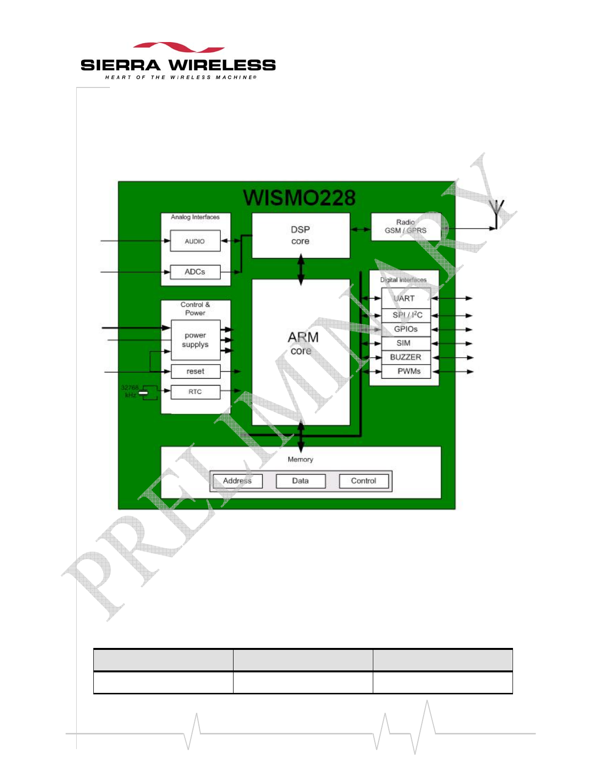
TheglobalarchitectureoftheWISMO228isshowninthefigurebelow.
Figure 1. Functional Architecture
RF Functionalities
TheRadioFrequency(RF)rangecomplieswiththePhaseIIGSM850/EGSM900/DCS1800/PCS1900
recommendation.Thefrequencyrangeforthetransmitbandandreceivebandarelistedinthetable
below.
Table 1. Frequency Range for Tx and Rx
Transmit Band (Tx) Receive Band (Rx)
GSM 850 824 to 849 MHz 869 to 894 MHz
WA_DEV_W228_PTS_002 Rev 001 Page 22 of 108
Product Technical Specification &
Customer Design Guidelines
Transmit Band (Tx) Receive Band (Rx)
E-GSM 900 880 to 915 MHz 925 to 960 MHz
DCS 1800 1710 to 1785 MHz 1805 to 1880 MHz
PCS 1900 1850 to 1910 MHz 1930 to 1990 MHz
TheRFpartoftheWISMO228isbasedonaspecificdualbandchipwhichincludes:
• aDigitallow‐IFreceiver
• adual‐bandLNA(LowNoiseAmplifier)
• anOffsetPLL(PhaseLockedLoop)transmitter
• aFrequencysynthesizer
• aDigitallyControlledCrystalOscillator(DCXO)
• aTx/RxFEM(Front‐EndModule)forquad‐bandGSM/GPRS
Baseband Functionalities
TheBasebandiscomposedofanARM9,aDSPandananalogelement(withaudiosignals,I/Q
signalsandADC).
Thecorepowersupplyis1.2Vandthedigitalpowersupplyis2.8V.

WA_DEV_W228_PTS_002 Rev 001 Page 23 of 108
Product Technical Specification &
Customer Design Guidelines
3. Interfaces
General Interfaces
TheWISMO228hasa46‐pincastellationconnection,whichprovidesaccesstoallavailable
interfaces.ThefollowingtableenumeratestheavailableinterfacesontheWISMO228.

WA_DEV_W228_PTS_002 Rev 001 Page 24 of 108
Product Technical Specification &
Customer Design Guidelines
Table 2. WISMO228 Interfaces
Available Interface Driven by
AT
commands
WA_DEV_W228_PTS_002 Rev 001 Page 25 of 108
Product Technical Specification &
Customer Design Guidelines
Available Interface Driven by
AT
commands
SPI Bus for Debug Trace ONLY
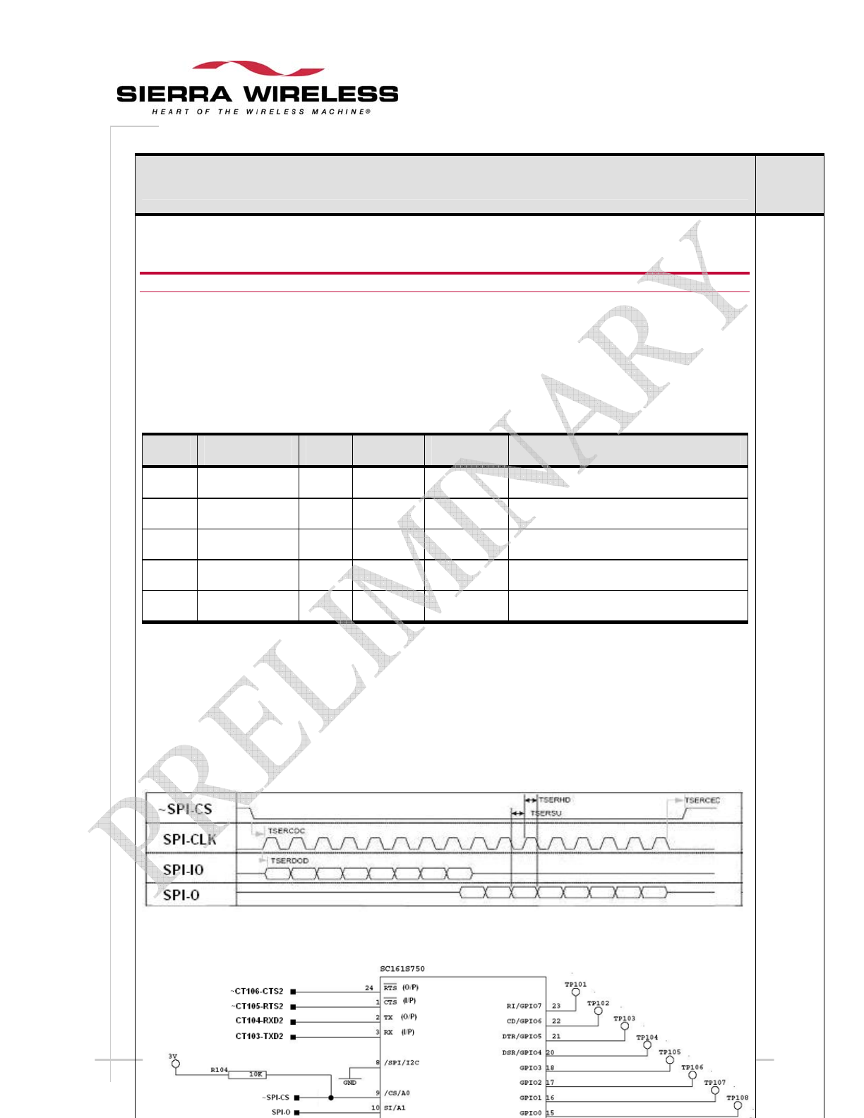
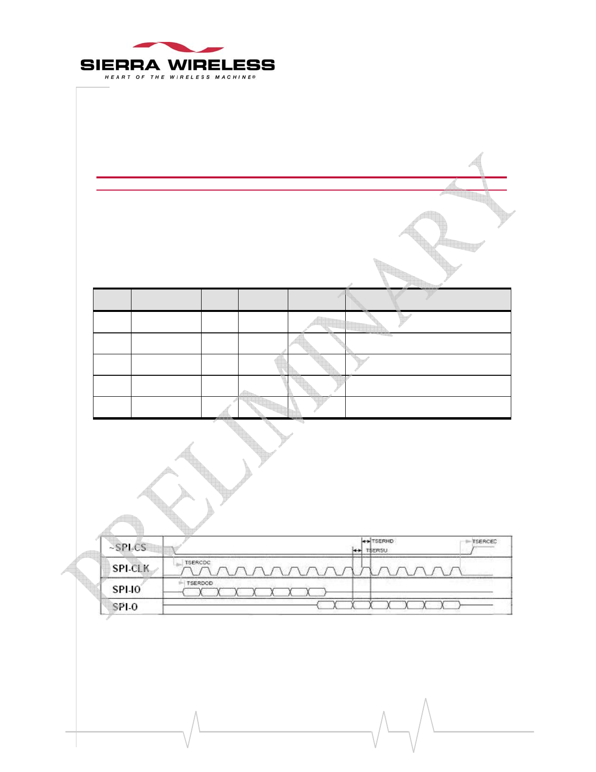
TheWISMO228providesoneSPIbusthroughthecastellationpin.
Caution: This interface is only used for monitoring trace for debug purposes.
Pin Description
ThefollowingtableprovidesthepindescriptionoftheSPIbus.
Table 3. SPI Bus Pin Description
Pin # Signal I/O I/O Type Reset State Description
13 SPI-IO I/O 2V8 Pull down SPI Serial input/output
14 SPI-O O 2V8 Pull down SPI Serial input
15 SPI-CLK O 2V8 Pull down SPI Serial Clock
17 ~SPI-CS O 2V8 Pull up SPI Enable
25 SPI-IRQ I 2V8 Pull down SPI Interrupt
AnSPI‐to‐UART2conversioncircuitisrequiredtoconverttheSPItracetoUART2.Also,theSPI‐IRQ
(pin25)isrequiredforinterrupt.Again,notethattheSPIinterfaceoftheWISMO228isnotopenfor
applicationuseotherthandebugtrace.
SPI Waveforms
Figure 2. SPI Timing Diagram
WA_DEV_W228_PTS_002 Rev 001 Page 26 of 108
Product Technical Specification &
Customer Design Guidelines
Available Interface Driven by
AT
commands
SIM Interface Yes
Error! Reference source not found. No*
Error! Reference source not found. Yes
Serial Interface (SPI) No
Analog to Digital Converter No*
Pulse-Width Modulators (PWMs) Yes
ON/~OFF No
PWM2 for Buzzer Output Yes
Module Ready Indication No
VBAT_RTC (Backup Battery) No
TX Burst Indication Signal No
Error! Reference source not found. No
* These interfaces will have AT command support in future versions.
WA_DEV_W228_PTS_002 Rev 001 Page 27 of 108
Product Technical Specification &
Customer Design Guidelines
Power Supply
Power Supply Description
ThepowersupplyisoneofthekeyelementsinthedesignofaGSMterminal.Duetotheburst
emissioninGSM/GPRS,thepowersupplymustbeabletodeliverhighcurrentpeaksinashorttime.
Duringthesepeaks,theripple(U
ripple
)onthesupplyvoltagemustnotexceedacertainlimit.Referto
Table4InputPowerSupplyVoltagefortheinputpowersupplyvoltagevalues.
ListedbelowarethecorrespondingradioburstratesforthedifferentGPRSclassesin
communicationmode.
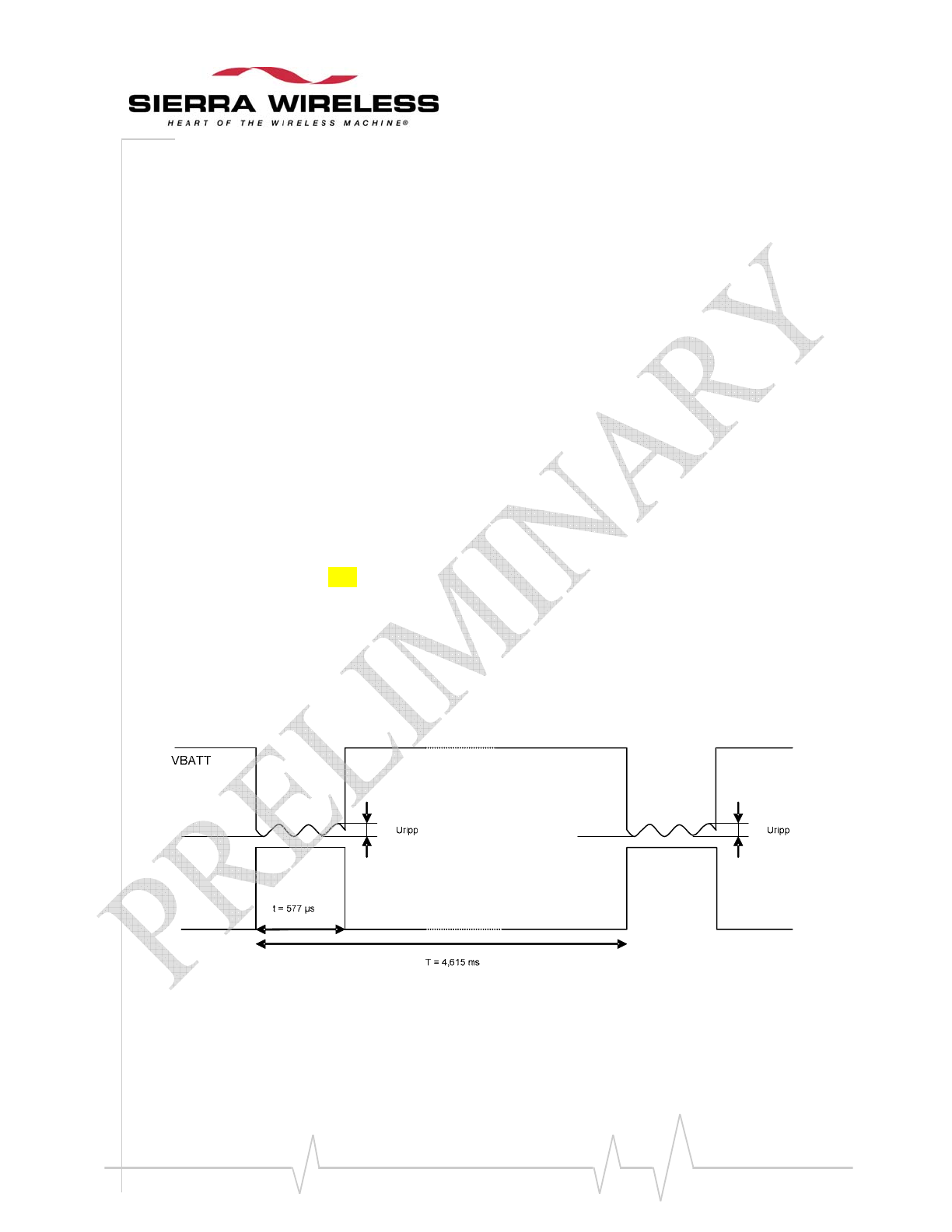
• AGSM/GPRSclass2terminalemits577μsradioburstsevery4.615ms.(SeeFigure5Power
SupplyDuringBurstEmission.)
• AGPRSclass10terminalemits1154μsradioburstsevery4.615ms.
VBATTprovidesforthefollowingfunctions:
• DirectlysuppliestheRFcomponentswith3.6V.Itisessentialtokeepaminimumvoltage
rippleatthisconnectioninordertoavoidanyphaseerror.
• Thepeakcurrent(TBDApeakinGSM/GPRSmode)flowswitharatioof:
1/8ofthetime(around577μsevery4.615msforGSM/GPRSclass2)
and
1/4ofthetime(around1154μsevery4.615msforGSM/GPRSclass10)
withtherisingtimeataround10μs.
• Internallyusedtoprovide,viaseveralregulators,thesupplyrequiredforthebaseband
signals.
Figure 5. Power Supply During Burst Emission
WA_DEV_W228_PTS_002 Rev 001 Page 28 of 108
Product Technical Specification &
Customer Design Guidelines
Electrical Characteristics
Table 4. Input Power Supply Voltage
Vmin Vnom Vmax ITYP Imax Ripple max (Uripp)
VBATT2 3.21 3.6 4.8 TBD TBD TBD
1: This value has to be guaranteed during the burst (with TBDA Peak in GSM or GPRS mode)
2: The maximum operating Voltage Stationary Wave Ratio (VSWR) is 1.5:1.
Note: When powering the WISMO228 with a battery, the total impedance (battery + protections + PCB)
should be less than 150m
Ω
.
Pin Description
Table 5. Power Supply Pin Description
Pin Numbers Signal
29,30 VBATT
20,22,23,26,28,31 GND
Application
TherejectfiltercanbeconnectedbetweenVBATTandthesupplysourcesifthesupplysourceis
noisy.
Caution: If the reject filter (C1+L1+C2) is an option, a capacitor (i.e. C2) is mandatory close to the VBATT.
Figure 6. Reject Filter Diagram
Thefollowingtableslisttherecommendedcomponentstouseinimplementingtherejectfilter.
WA_DEV_W228_PTS_002 Rev 001 Page 29 of 108
Product Technical Specification &
Customer Design Guidelines
C1,C2: 10μF+/‐20%
Component Manufacturer
GRM21BR60J106KE19L MURATA
CM21X5R106M06AT KYOCERA
JMK212BJ106MG-T TAYO YUDEN
C2012X5R0J106MT TDK
L1: 220nH+/‐5%
Component Manufacturer
0805CS-221XJLC COILCRAFT
0805G221J E STETCO
WA_DEV_W228_PTS_002 Rev 001 Page 30 of 108
Product Technical Specification &
Customer Design Guidelines
Power Consumption
ThepowerconsumptionlevelsoftheWISMO228varydependingontheoperatingmodeusedand
thefollowingsub‐sectionsdescribethepowerconsumptionvaluesoftheWISMO228whenrunning
invariousoperatingmodesandRFbands.
Various Operating Modes
RefertothefollowingtableforthelistofavailableoperatingmodesontheWISMO228.
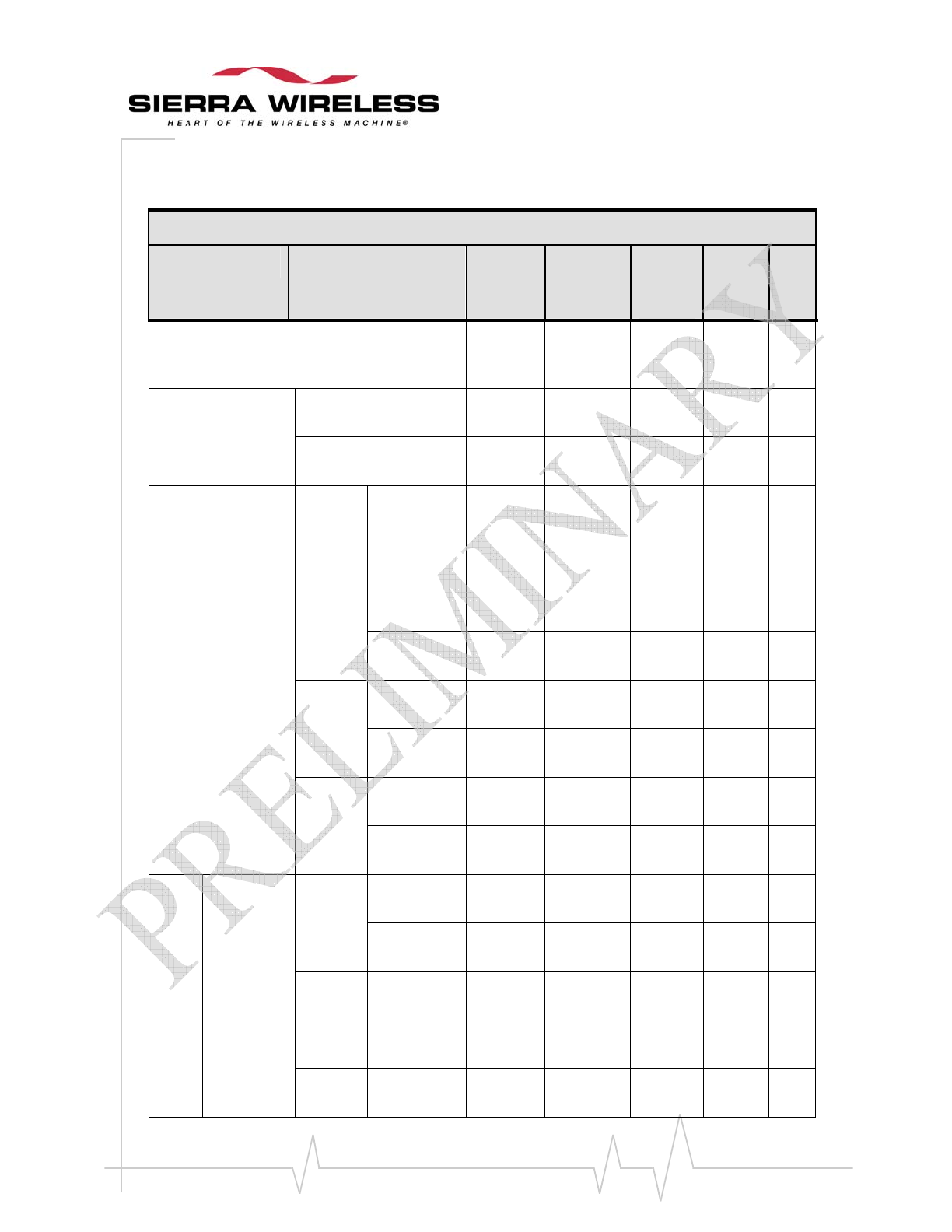
Table 6. WISMO228 Operating Modes
Mode Description
OFF Mode When VBATT power is supplied to the WISMO228 but it has not yet been powered
ON.
Alarm Mode
When alarm clock is set for the WISMO228 with ALL of the following conditions:
• before time is up
• with AT + CPOF having been entered from a computer that is connected to the
WISMO228
• with the ON/~OFF signal being left open (remains at HIGH level)
Idle Mode When the WISMO228 has a location update with a live network but with no
GSM/GPRS connection, while the UART interface is in sleep mode.
Connected Mode The WISMO228 has GSM voice codec connection with a live network.
Transfer Mode The WISMO228 has GPRS data transfer connection with a live network.
NotethattherearetwodifferentmethodsofenteringsleepmodethroughtheATcommand,
AT+PSSLEEP.
• AT+PSSLEEP=0
TheentryofsleepmodeiscontrolledbytheleveloftheDTRsignalandthe
firmware.
TheWISMO228willneverentersleepmodewhentheDTR(viewedfromthe
moduleside)isofLOWvoltagelevel.Ontheotherhand,theWISMO228willenter
sleepmodewhentheDTR(viewedfromthemoduleside)isofHIGHvoltagelevel.
TowaketheWISMO228up,itisnecessarytotoggletheDTR(viewedfrommodule
side)fromHIGHtoLOWvoltagelevel.
Thismethodshouldbeusediftheapplicationneedstoforbidtheentryofsleep
mode.
• AT+PSSLEEP=1
Theentryofsleepmodeiscontrolledjustbythefirmware.
WA_DEV_W228_PTS_002 Rev 001 Page 31 of 108
Product Technical Specification &
Customer Design Guidelines
WhentheWISMO228hashadnoactivitiesforacertainperiodoftime,itwillenter
sleepmodeautomatically,regardlessoftheDTRlevel.
AnyASCIIcharacterontheUARTcanwaketheWISMO228up.
RefertotheWISMO218ATCommandsManualformoreinformationabouttheAT+PSSLEEP
command.
Power Consumption Values
ThreeVBATTvalueswereusedtomeasurethepowerconsumptionoftheWISMO228:VBATTmin
(3.2V),VBATTmax(4.8V)andVBATTtyp(3.6V).Boththeaveragecurrentandthemaximumcurrent
peakswerealsomeasuredforallthreeVBATTvalues.
ThefollowingconsumptionvalueswereobtainedbyperformingmeasurementsonWISMO228
samplesatatemperatureof25°Cwiththeassumptionofa50ΩRFoutput.
Note: Power consumption performance is software related. The results listed below are based on the
software version TBD.
WA_DEV_W228_PTS_002 Rev 001 Page 32 of 108
Product Technical Specification &
Customer Design Guidelines
Table 7. WISMO228 Power Consumption
WISMO228 Power Consumption
Operating Mode Parameters IMIN
average
VBATT=4.8V
INOM
average
VBATT=3.6V
IMAX
average
VBATT=3.2
V
IMAX peak Unit
Off Mode* TBD TBD TBD TBD µA
Alarm Mode TBD TBD TBD TBD µA
Idle Mode** Paging 2 (Rx burst
occurrence ~0.5s) TBD TBD TBD TBD mA
Paging 9 (Rx burst
occurrence ~2s) TBD TBD TBD TBD mA
Connected Mode
850 MHz
PCL5 (TX
power 33dBm) TBD TBD TBD TBD mA
PCL19 (TX
power 5dBm) TBD TBD TBD TBD mA
900 MHz
PCL5 (TX
power 33dBm) TBD TBD TBD TBD mA
PCL19 (TX
power 5dBm) TBD TBD TBD TBD mA
1800 MHz
PCL0 (TX
power 30dBm) TBD TBD TBD TBD mA
PCL15 (TX
power 0dBm) TBD TBD TBD TBD mA
1900 MHz
PCL0 (TX
power 30dBm) TBD TBD TBD TBD mA
PCL15 (TX
power 0dBm) TBD TBD TBD TBD
mA
GPRS Transfer
Mode class
8 (4Rx/1Tx)
850 MHz
Gam.3 (TX
power 33dBm) TBD TBD TBD TBD mA
Gam.17 (TX
power 5dBm) TBD TBD TBD TBD
mA
900 MHz
Gam.3 (TX
power 33dBm) TBD TBD TBD TBD mA
Gam.17 (TX
power 5dBm) TBD TBD TBD TBD
mA
1800 MHz Gam.3 (TX
power 30dBm) TBD TBD TBD TBD mA
WA_DEV_W228_PTS_002 Rev 001 Page 33 of 108
Product Technical Specification &
Customer Design Guidelines
Gam.18 (TX
power 0dBm) TBD TBD TBD TBD
mA
1900 MHz
Gam.3 (TX
power 30dBm) TBD TBD TBD TBD mA
Gam.18 (TX
power 0dBm) TBD TBD TBD TBD
mA
Transfer
Mode class
10 (3Rx/2Tx)
850 MHz
Gam.3 (TX
power 33dBm) TBD TBD TBD TBD mA
Gam.17 (TX
power 5dBm) TBD TBD TBD TBD
mA
900 MHz
Gam.3 (TX
power 33dBm) TBD TBD TBD TBD mA
Gam.17 (TX
power 5dBm) TBD TBD TBD TBD
mA
1800 MHz
Gam.3 (TX
power 30dBm) TBD TBD TBD TBD mA
Gam.18 (TX
power 0dBm) TBD TBD TBD TBD
mA
1900 MHz
Gam.3 (TX
power 30dBm) TBD TBD TBD TBD mA
Gam.18 (TX
power 0dBm) TBD TBD TBD TBD
mA
* Current consumption in OFF mode is measured with BAT-RTC being left open.
** Idle Mode consumption depends on the SIM card used. Some SIM cards respond faster than others, in which
case the longer the response time is, the higher the consumption is.
Note: TX means that the current peak is the RF transmission burst (Tx burst).
RX means that the current peak is the RF reception burst (Rx burst), in GSM mode only (worst case).
4. Refer to section 1
WA_DEV_W228_PTS_002 Rev 001 Page 34 of 108
Product Technical Specification &
Customer Design Guidelines
ConsumptionMeasurementProcedureformoreinformationregardingconsumptionmeasurement
procedures.
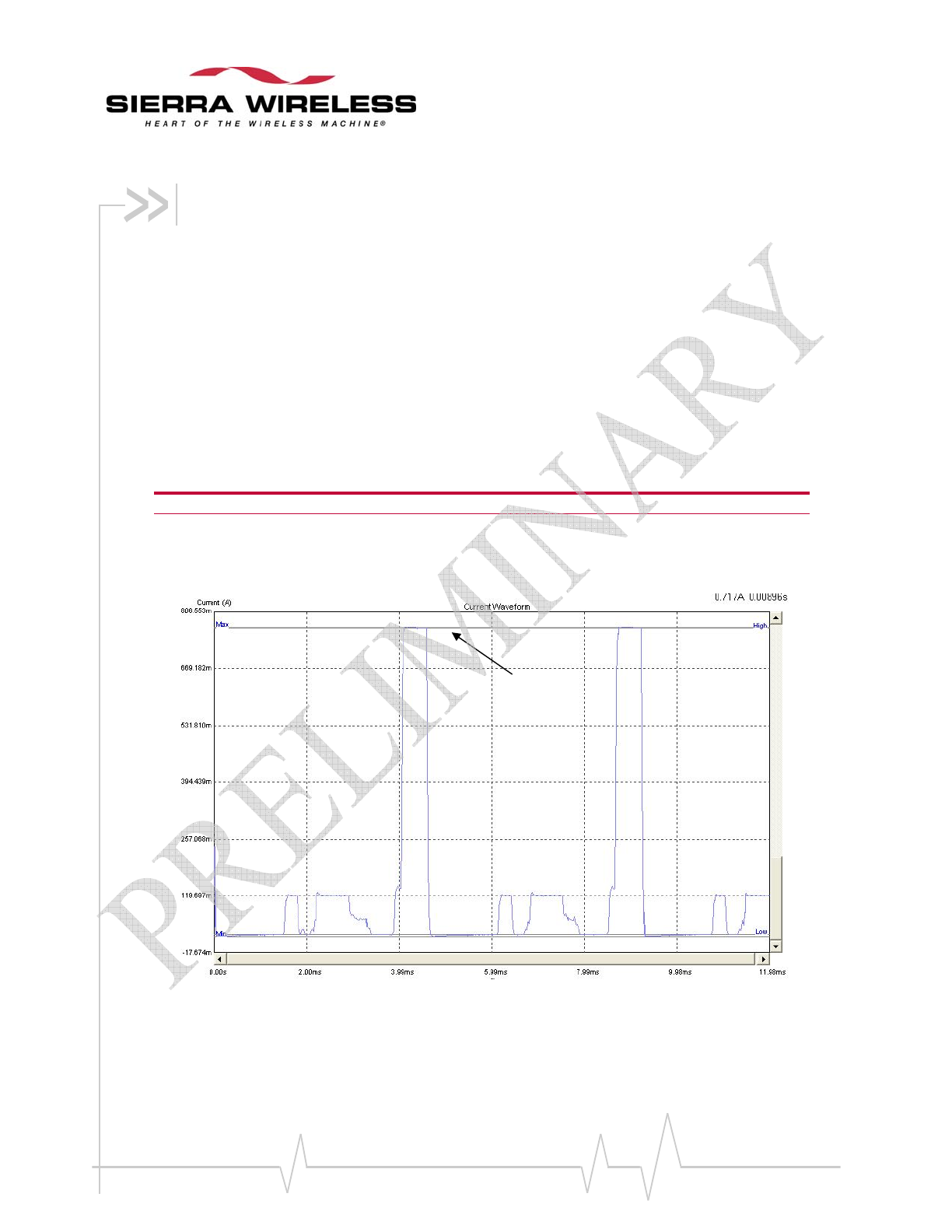
Consumption Waveform Samples
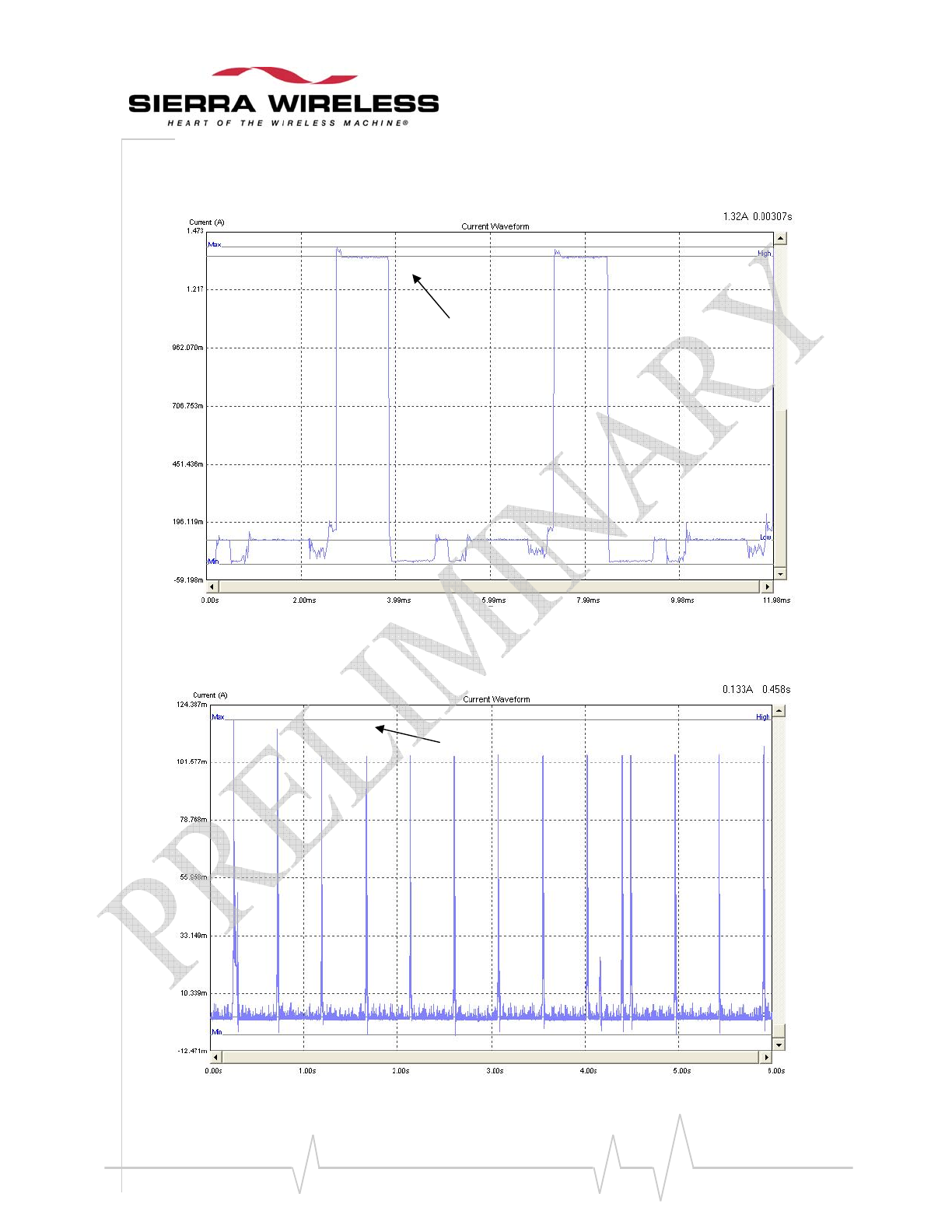
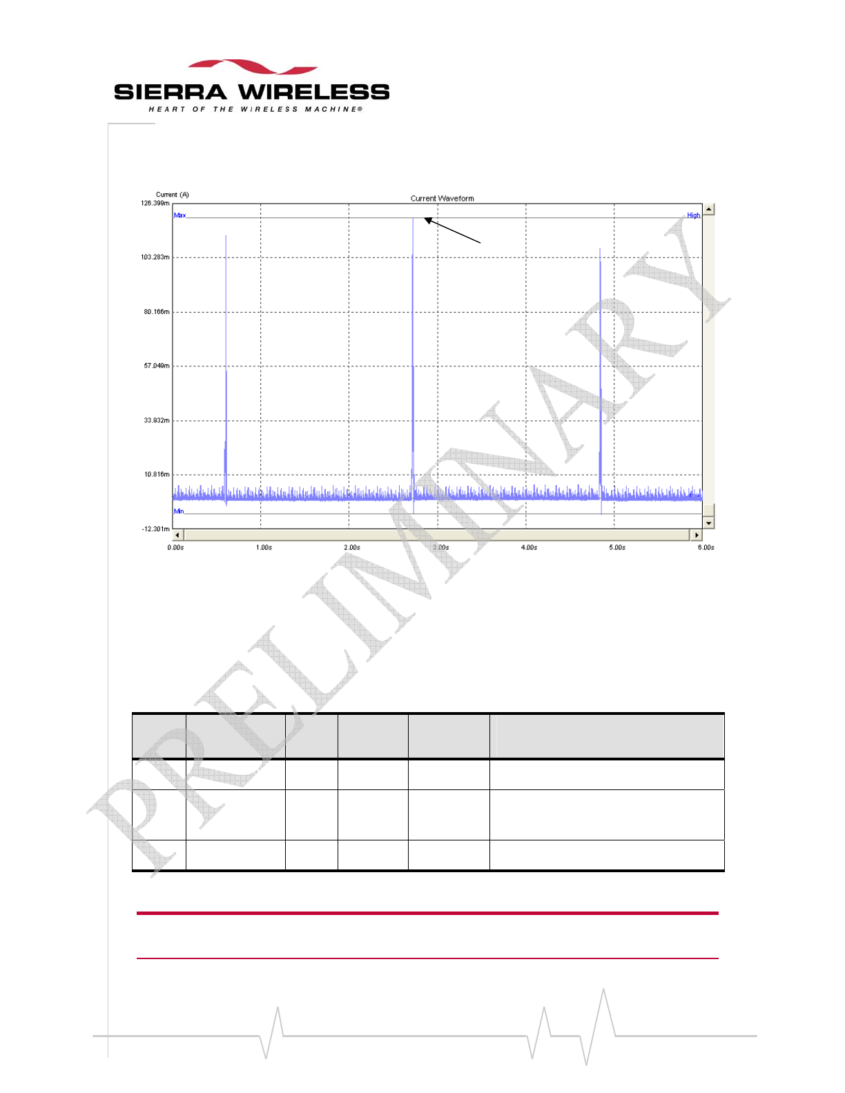
TheconsumptionwaveformspresentedbelowhaveatypicalVBATTvoltageof3.6Vandareforan
EGSM900networkconfiguration.
Foursignificantoperatingmodeconsumptionwaveformsareshowninthefollowingsubsections,
namely:
• ConnectedMode(PCL5:Txpower33dBm)
• Transfermode(GPRSclass10,gam.3:Txpower33dBm)
• Idlemode(Paging2)
• Idlemode(Paging9)
Note: The following diagrams only show the waveform of the current, and not the exact values.
Connected Mode Current Waveform
TXPEAK
WA_DEV_W228_PTS_002 Rev 001 Page 35 of 108
Product Technical Specification &
Customer Design Guidelines
Transfer Mode Class 10 Current Waveform
Idle Mode Page 2 Current Waveform
RXPEAK
TXPEAK
WA_DEV_W228_PTS_002 Rev 001 Page 36 of 108
Product Technical Specification &
Customer Design Guidelines
Idle Mode Page 9 Current Waveform
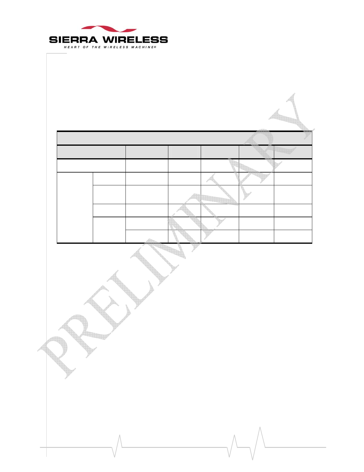
Recommendations for Less Consumption
Forbetterpowerconsumption,inparticularforthequiescentcurrent,itisrecommendedtodrive
theGPIOsasshowninthetablebelow.
Table 8. Consumption/Software Driver Recommendations
Pin # Signal I/O I/O Type Reset State Recommended SW Driver (Logic
Level Output State)
16 GPIO3 I/O 2V8 Pull up 1
19 GPIO5 I/O 2V8 Z** Input: 0
Output: 1
24 GPIO1 I/O 2V8 Pull up 1
** When GPIO5 is used as a general purpose output, it is necessary to have an external pull up resistor
connecting to a 2.8V source. The resistance value depends on the current drain required by the application side.
Note: GPIO2 is dedicated for WISMO_READY and is not open as a GPIO for customer use.
GPIO4 is dedicated for TX burst indication and is not open as GPIO for customer use.
RXPEA
K
WA_DEV_W228_PTS_002 Rev 001 Page 37 of 108
Product Technical Specification &
Customer Design Guidelines
Electrical Information for Digital I/O
ThefollowingtabledescribestheelectricalcharacteristicsofthedigitalI/Os(interfacessuchas
GPIO,SPI,etc.)availableontheWISMO228.
Table 9. Electrical Characteristics of Digital I/Os
2.8Volt Type (2V8)
Parameter Conditions I/O Type Minimum Typical Maximum
Internal 2.8V power supply VCC_2V8 2.7V 2.8V 2.95V
Input/Output
Pin
VIL CMOS -0.4V* - 0.4V
VIH CMOS 2.4V - VCC_2V8 +
0.4V
VOL CMOS - - 0.1V
VOH
CMOS 2.7V - -
IOH = 4mA CMOS 2.4V - -
* Absolute maximum ratings
WA_DEV_W228_PTS_002 Rev 001 Page 38 of 108
Product Technical Specification &
Customer Design Guidelines
SPI Bus for Debug Trace ONLY
TheWISMO228providesoneSPIbusthroughthecastellationpin.
Caution: This interface is only used for monitoring trace for debug purposes.
Pin Description
ThefollowingtableprovidesthepindescriptionoftheSPIbus.
Table 10. SPI Bus Pin Description
Pin # Signal I/O I/O Type Reset State Description
13 SPI-IO I/O 2V8 Pull down SPI Serial input/output
14 SPI-O O 2V8 Pull down SPI Serial input
15 SPI-CLK O 2V8 Pull down SPI Serial Clock
17 ~SPI-CS O 2V8 Pull up SPI Enable
25 SPI-IRQ I 2V8 Pull down SPI Interrupt
AnSPI‐to‐UART2conversioncircuitisrequiredtoconverttheSPItracetoUART2.Also,theSPI‐
IRQ(pin25)isrequiredforinterrupt.Again,notethattheSPIinterfaceoftheWISMO228isnot
openforapplicationuseotherthandebugtrace.
SPI Waveforms
Figure 7. SPI Timing Diagram
WA_DEV_W228_PTS_002 Rev 001 Page 39 of 108
Product Technical Specification &
Customer Design Guidelines
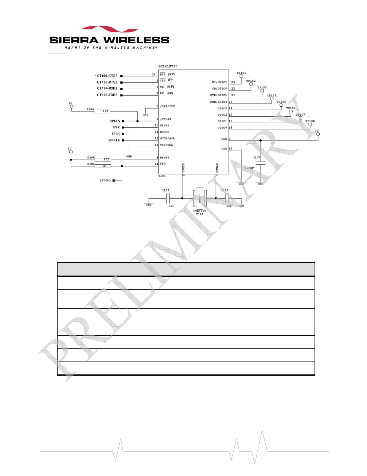
Figure 8. Example of an SPI to UART2 Interface Conversion Implementation
ThefollowingtableliststherecommendedcomponentstouseinimplementingtheSPItoUART2
interface.
Component Description/Details Manufacturer
U103 SC16IS750IPW NXP Semiconductors
X101 3, 6864MHz 86SMX surface mount crystal (971-
3131) Farnell
R104, R105 10KΩ
R106 1KΩ
C105 22pF
C106 33pF
C107 100nF
AfterconvertingtheSPIsignaltoaUARTsignal,aUARTtransceivercircuitryisneededto
communicatethisUARTsignaltotheDTE.

WA_DEV_W228_PTS_002 Rev 001 Page 40 of 108
Product Technical Specification &
Customer Design Guidelines
Figure 9. Example of an RS-232 Level Shifter Implementation for UART2
ThefollowingtableliststherecommendedcomponentstouseinimplementingaUARTtransceiver
circuitry.
Component Description/Details Manufacturer
U200 LTC2804IGN-1 LINEAR TECHNOLOGY
L200 LQH2M CN100K02L MURATA
J200 096615276119 SUBD9F HARTING
R202 NC
R204 100KΩ
C200 1µF
C201 220nF
C207 1µF
C208 1µF
Note: It is recommended to make SPI signals accessible for diagnostics by reserving some test points, for
example.
WA_DEV_W228_PTS_002 Rev 001 Page 41 of 108
Product Technical Specification &
Customer Design Guidelines
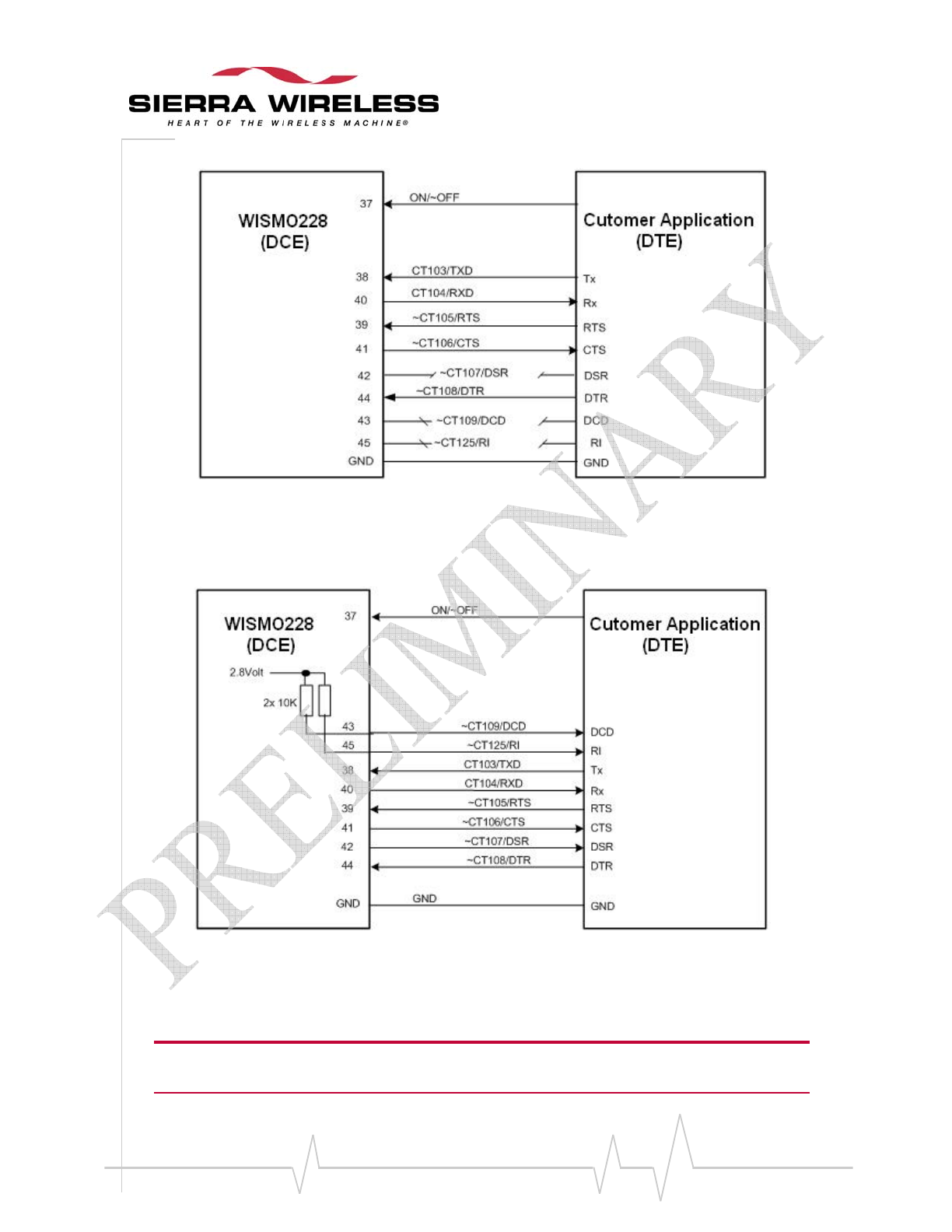
Main Serial Link (UART)
Aflexible8‐wireserialinterfaceisavailableontheWISMO228thatcomplieswiththeV24protocol
signaling,butnotwiththeV28(electricalinterface)protocol,duetoits2.8Vinterface.
ThesupportedbaudratesoftheUARTare1200,2400,4800,9600,19200,38400,57600and115200
Kbits,withautobauding;andthesignalsusedbytheUARTare:
• TXdata(CT103/TXD)
• RXdata(CT104/RXD)
• RequestToSend(~CT105/RTS)
• ClearToSend(~CT106/CTS)
• DataTerminalReady(~CT108/DTR)
• DataSetReady(~CT107/DSR)
• DataCarrierDetect(~CT109/DCD)
• RingIndicator(~CT125/RI).
Pin Description
ThefollowingtableprovidesthepindescriptionsoftheUARTinterface.
Table 11. Main Serial Link Pin Description
* According to PC (DTE) view
Note: The rising time and falling time of the reception signals (mainly CT103/TXD) have to be less than
300ns.
The WISMO228 is designed to operate using all the serial interface signals and it is recommended to
Pin # Signal* I/O I/O Type Reset State Description
38 CT103/TXD I 2V8 1 Transmit serial data
39 ~CT105/RTS I 2V8 1 Request To Send
40 CT104/RXD O 2V8 0 Receive serial data
41 ~CT106/CTS O 2V8 0 Clear To Send
42 ~CT107/DSR O 2V8 1 Data Set Ready
43 ~CT109/DCD O 2V8 1 Data Carrier Detect
44 ~CT108/DTR I 2V8 1 Data Terminal Ready
45 ~CT125/RI O 2V8 1 Ring Indicator
GND GND Ground

WA_DEV_W228_PTS_002 Rev 001 Page 42 of 108
Product Technical Specification &
Customer Design Guidelines
use ~CT105/RTS and ~CT106/CTS for hardware flow control in order to avoid data corruption during
transmissions.
5-wire Serial Interface Hardware Design
Thesignalsusedinthisinterfacehardwaredesignareasfollows:
• CT103/TXD
• CT104/RXD
• ~CT105/RTS
• ~CT106/CTS
• ‐CT108/DTR
Thesignal~CT108/DTRmustbemanagedfollowingtheV24protocolsignalingifidlemodeistobe
used.
Foradetailedconfiguration,refertoFigure13ExampleofV24/CMOSSerialLinkImplementation
fora5‐wireUART.
Note: All signals are specified according to PC (DTE) view.
4-wire Serial Interface Hardware Design
Thesignalsusedinthisinterfacehardwaredesignareasfollows:
• CT103/TXD
• CT104/RXD
• ~CT105/RTS
• ~CT106/CTS
Thesignal~CT108/DTRcanbeloopedbackto~CT107/DSRfromboththeWISMO228sideandfrom
theDTEside.
Foradetailedconfiguration,refertoFigure12ExampleofV24/CMOSSerialLinkImplementation
fora4‐wireUART.
Note: All signals are specified according to PC (DTE) view.
2-wire Serial Interface Hardware Design
Note: Although this case is possible for a connected external chip, it is not recommended.
All signals are specified according to PC (DTE) view.
Thesignalsusedinthisinterfacehardwaredesignareasfollows:
• CT103/TXD

WA_DEV_W228_PTS_002 Rev 001 Page 43 of 108
Product Technical Specification &
Customer Design Guidelines
• CT104/RXD
Signals~CT105/RTSand~CT106/CTSarenotusedinthisconfiguration.ConfiguretheATcommand
AT+IFC=0,0todisabletheflowcontrolfunctionontheWISMO228.RefertotheWISMO218AT
CommandsManualformoreinformationaboutconfiguringATcommands.
Also,
• Thesignal~CT108/DTRcanbeloopedbackto~CT107/DSRfromboththeWISMO228side
andfromtheDTEside.
• Thesignal~CT105/RTScanbeloopedbackto~CT106/CTSfromboththeWISMO228side
andfromtheDTEside.
• Theflowcontrolmechanismhastobemanagedfromthecustomerside.
Foradetailedconfiguration,refertoFigure11ExampleofV24/CMOSSerialLinkImplementation
fora2‐wireUART.
The loop back connection of ~CT108/DTR to
~CT107/DSR is not allowed when
AT+PSSLEEP=0 is used, for which sleep mode
entry is ~CT108/DTR level dependent. For more
details, refer to the discussion about AT + PSSLEEP
= 0 in section 0

WA_DEV_W228_PTS_002 Rev 001 Page 44 of 108
Product Technical Specification &
Customer Design Guidelines
Power Consumption.
In order to go to sleep mode properly under this
instead. For more details, refer to the discussion
about AT + PSSLEEP = 1 in section 0
WA_DEV_W228_PTS_002 Rev 001 Page 45 of 108
Product Technical Specification &
Customer Design Guidelines
Note: Power Consumption.
Application
ThelevelshiftermustbeaV28electricalsignalcompliantwith2.8V.
Figure 10. Example of RS-232 Level Shifter Implementation for UART
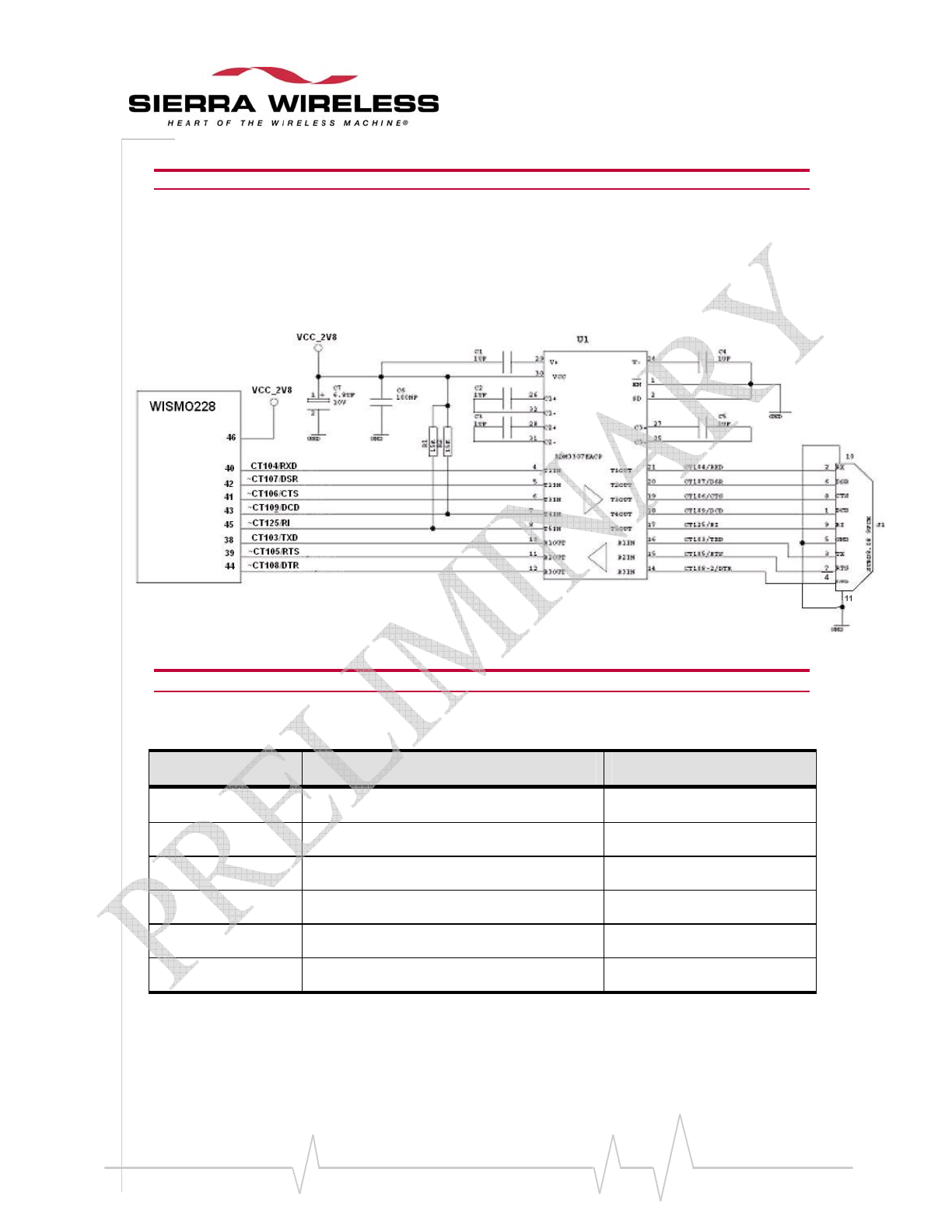
Note: The U1 chip also protects the WISMO228 against ESD (air discharge) at 15KV.
Thefollowingtableliststherecommendedcomponentstouseinimplementingalevelshifter
UART.
Component Description/Details Manufacturer
R1, R2 15KΩ
C1, C2, C3, C4, C5 1µF
C6 100nF
C7 6.8uF TANTAL 10V CP32136 AVX
U1 ADM3307EACP ANALOG DEVICES
J1 SUB-D9 female
R1andR2arenecessaryonlyduringtheResetstatetoforcethe~CT125/RIand~CT109/DCDsignals
toHIGHlevel.
TheADM3307EACPcanbepoweredbytheVCC_2V8(pin46)oftheWISMO228orbyanexternal
regulatorat2.8V.
WA_DEV_W228_PTS_002 Rev 001 Page 46 of 108
Product Technical Specification &
Customer Design Guidelines
ItisnotnecessarytouselevelshifterswhentheUARTinterfaceisdirectlyconnectedtoahost
processor.Refertothefollowingsectionsforstepsonhowtoconnecttheinterfaceusingother
designimplementations.
V24/CMOS Possible Design
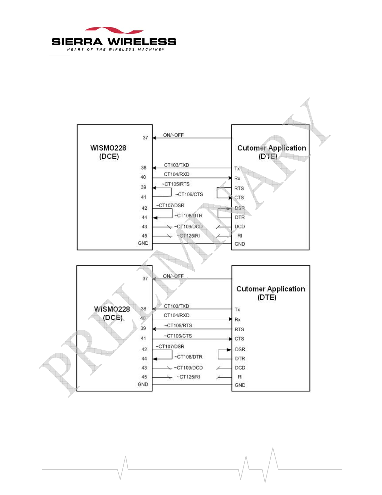
Figure 11. Example of V24/CMOS Serial Link Implementation for a 2-wire UART
Figure 12. Example of V24/CMOS Serial Link Implementation for a 4-wire UART
WA_DEV_W228_PTS_002 Rev 001 Page 47 of 108
Product Technical Specification &
Customer Design Guidelines
Figure 13. Example of V24/CMOS Serial Link Implementation for a 5-wire UART
ThedesignsshowninFigure11,Figure12andFigure13arebasicdesigns.BoththeDCDandtheRI
canbeleftopenwhennotused.
However,amoreflexibledesigntoaccessthisseriallinkwithallmodemsignalsisshownbelow.
Figure 14. Example of a Full Modem V24/CMOS Serial Link Implementation for a full UART
Aninternal10KΩpull‐upresistorisconnectedonbothRIandDCDtosetthesignalstoHIGHlevel
duringtheResetstate.
TheUARTinterfaceisa2.8Vtype,butitis3Vtolerant.
Note: The WISMO228 UART is designed to operate using all the serial interface signals. In particular, it is
recommended to use ~CT105/RTS and ~CT106/CTS for hardware flow control in order to avoid data
corruption during transmission.
WA_DEV_W228_PTS_002 Rev 001 Page 48 of 108
Product Technical Specification &
Customer Design Guidelines
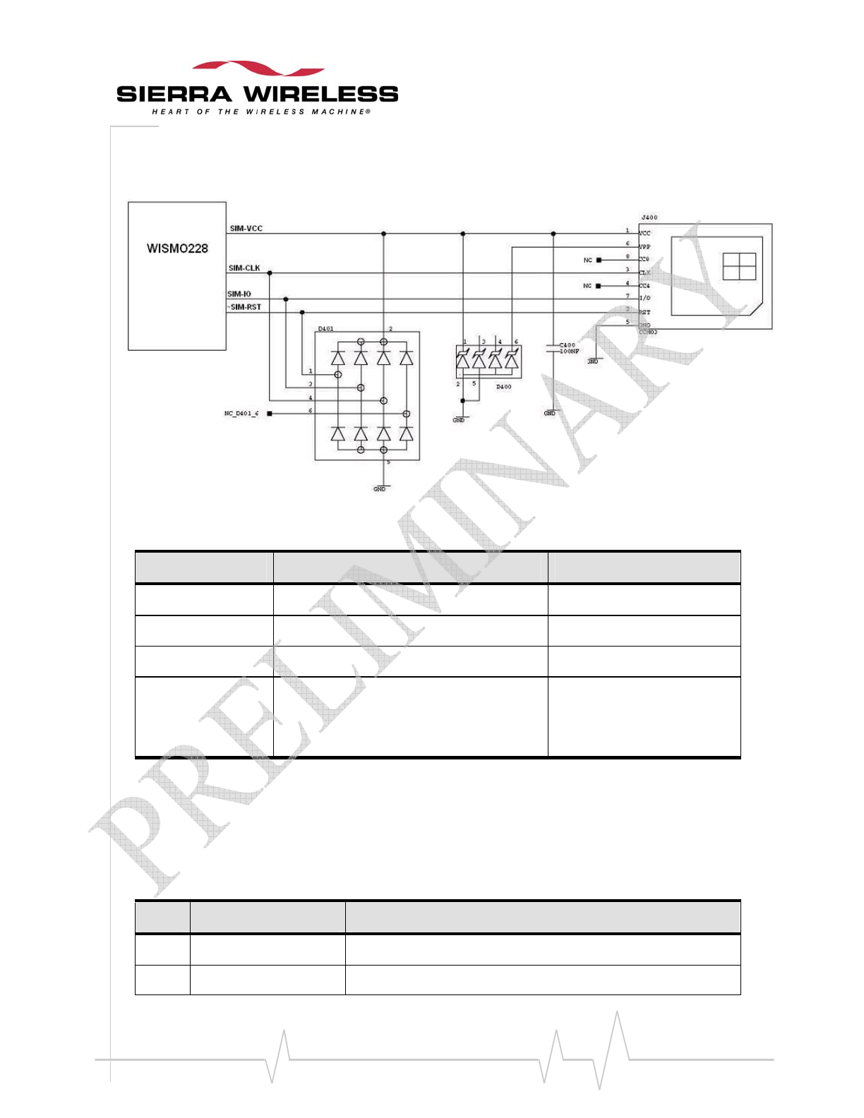
SIM Interface
TheSubscriberIdentificationModulecanbedirectlyconnectedtotheWISMO228throughthis
dedicatedinterface.
Thisinterfacecontrolsboth1.8Vand3VSIMcardsandisfullycompliantwithGSM11.11
recommendationsconcerningSIMfunctions.
TheSIMusesfoursignals,namely:
• SIM‐VCC:SIMpowersupply
• ~SIM‐RST:reset
• SIM‐CLK:clock
• SIM‐IO:I/Oport
ItisrecommendedtoaddTransientVoltageSuppressor(TVS)diodesonthesignalsconnectedto
theSIMsocketinordertopreventanyElectrostaticDischarge.TVSdiodeswithlowcapacitance
(lessthan10pF)havetobeconnectedontheSIM‐CLKandSIM‐IOsignalstoavoidanydisturbance
fromtherisingandfallingedgeofthesignals.TVSdiodesaremandatoryfortheFullType
ApprovalandtheymustbeplacedasclosetotheSIMsocketaspossible.
TherecommendedlowcapacitancediodearraytouseistheDALC208SC6fromSTMicroelectronics.
Electrical Characteristics
ThefollowingtabledescribestheelectricalcharacteristicsoftheSIMinterface.
Table 12. Electrical Characteristics of the SIM Interface
Parameters Conditions Minimum Typical Maximum Unit
SIM-IO VIH IIH = ± 20µA 0.7xVSIM - - V
SIM-IO VIL IIL = 1mA - - 0.4 V
~SIM-RST, SIM-CLK
VOH Source current = 20µA 0.9xVSIM - - V
SIM-IO VOH Source current = 20µA 0.8xVSIM - - V
~SIM-RST, SIM-IO, SIM-
CLK
VOL
Sink current =
-200µA - - 0.4 V
SIM-VCC Output Voltage SIM-VCC = 2.9V 2.75 2.9 3.0 V
WA_DEV_W228_PTS_002 Rev 001 Page 49 of 108
Product Technical Specification &
Customer Design Guidelines
Parameters Conditions Minimum Typical Maximum Unit
SIM-VCC = 1.8V 1.65 1.8 1.95 V
SIM-VCC current
full-power mode - - 20 mA
Sleep mode with 32kHz
system clock enabled. - - 3 mA
SIM-CLK Rise/Fall Time Loaded with 30pF and ESD
protection diode - 25 50 ns
~SIM-RST, Rise/Fall
Time Loaded with 30pF and ESD
protection diode - 45 - ns
SIM-IO Rise/Fall Time
Loaded with 30pF and ESD
protection diode
- 0.2 1 µs
SIM-CLK Frequency Loaded with 30pF - - 3.25 MHz
Pin Description
ThefollowingtableprovidesthepindescriptionoftheSIMinterface.
Table 13. SIM Interface Pin Description
Pin # Signal I/O I/O Type Reset State Description Multiplexed
8 SIM-VCC O 2V9 / 1V8 SIM Power Supply No
9 SIM-CLK O 2V9 / 1V8 0 SIM Clock No
10 SIM-IO I/O 2V9 / 1V8 Pull up SIM Data No
11 ~SIM-RST O 2V9 / 1V8 0 SIM Reset No
WA_DEV_W228_PTS_002 Rev 001 Page 50 of 108
Product Technical Specification &
Customer Design Guidelines
Application
Figure 15. Example of a SIM Socket Implementation
ThefollowingtableliststherecommendedcomponentstouseinimplementingtheSIMsocket.
Component Description/Details Manufacturer
C400 100nF
D400 ESDA6V1SC6 ST
D401 DALC208SC6 SGS-THOMSON
J400
ITT CANNON CCM03 series
(Refer to the SIM Card Reader sub-section of
section 1 Error! Not a valid result for table. for
more information)
CANNON
SIM Socket Connection
ThefollowingtableprovidesthepindescriptionoftheSIMsocket.
Table 14. SIM Socket Pin Description
Pin # Signal Description
1 VCC SIM-VCC
2 RST ~SIM-RST
WA_DEV_W228_PTS_002 Rev 001 Page 51 of 108
Product Technical Specification &
Customer Design Guidelines
Pin # Signal Description
3 CLK SIM-CLK
4 CC4 Not connected
5 GND GROUND
6 VPP Not connected
7 I/O SIM-IO
8 CC8 Not connected
Note: CC4 and CC8 are not connected as the WISMO228 does not support the SIM detect feature.
WA_DEV_W228_PTS_002 Rev 001 Page 52 of 108
Product Technical Specification &
Customer Design Guidelines
General Purpose Input/Output
TheWISMO228providesuptothreeGeneralPurposeI/Os.Theyareusedtocontrolanyexternal
devicesuchasanLCDoraKeyboardbacklight.
TheseGPIOsofferthepossibilitytoreadthepinstatewhatevertheirdirectionmaybe.
Pin Description
ThefollowingtableprovidesthepindescriptionoftheGPIOs.
Table 15. GPIO Pin Descriptions
Pin # Signal I/O I/O Type Reset State
16 GPIO3 I/O 2V8 Pull up
19 GPIO5 I/O 2V8 Pull down
24 GPIO1 I/O 2V8 Pull up
WhenGPIO5isusedasageneralpurposeoutput,itisnecessarytohaveanexternalpullupresistor
connectedtoa2.8Vsource.Theresistancevaluewilldependonthecurrentdrainrequiredbythe
application.
Note: GPIO2 is dedicated for WISMO_READY and is not open as GPIO for customer use.
GPIO4 is dedicated for TX burst indication and is not open as GPIO for customer use.
WA_DEV_W228_PTS_002 Rev 001 Page 53 of 108
Product Technical Specification &
Customer Design Guidelines
Analog to Digital Converter
OneAnalogtoDigitalConverterinput,AUX‐ADC0,isprovidedbytheWISMO228forcustomer
applications.Itisa10‐bitresolutionconverter,rangingfromeither0to1Vor0to3V,dependingon
thegeneralpurposeinputmode.
Electrical Characteristics
ThefollowingtabledescribestheelectricalcharacteristicsoftheADCinterface.
Table 16. Electrical Characteristics of the ADC Interface
Parameters Minimum Typical Maximum Unit
Resolution - 10 - bits
Sampling frequency - - 200 kHz
Input signal range
1 general purpose input 0 - 1 V
1 general purpose input in div-by-3
mode 0 - 3 V
Integral non-linearity (INL) -2.5 - +2.5 bit
Differential non-linearity (DNL) -1 - +3 bit
Input impedance
input resistance 120 - - KΩ
input capacitance - - 10 pF
Pin Description
ThefollowingtableprovidesthepindescriptionoftheAnalogtoDigitalConverterinterface.
Table 17. Analog to Digital Converter Pin Description
Pin # Signal I/O I/O Type Description
5 AUX-ADC0 I Analog A/D converter
Caution: The AUX-ADC0 pin is ESD sensitive and it is a must to add ESD protection to this pin once it is
externally accessible. The recommended ESD protection to use is the AVL5M02200 from Amotech.
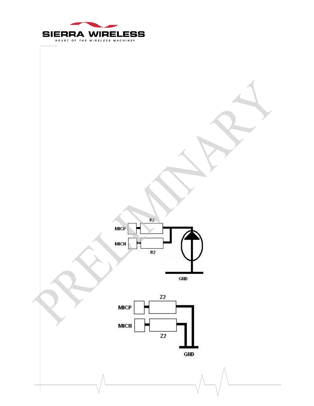
WA_DEV_W228_PTS_002 Rev 001 Page 54 of 108
Product Technical Specification &
Customer Design Guidelines
Analog Audio Interface
TheWISMO228supportsonemicrophoneinputandonespeakeroutput.Italsoincludesanecho
cancellationfeaturewhichallowshandsfreefunction.
Insomecases,ESDprotectionmustbeaddedontheaudiointerfacelines.
Microphone Features
Themicrophone,MIC,canhaveeitherasingle‐endedoradifferentialconnection.However,itis
stronglyrecommendedtouseadifferentialconnectioninsteadofasingle‐endedconnectioninorder
torejectcommonmodenoiseandTDMAnoise.
Whenusingasingle‐endedconnection,besuretohaveaverygoodgroundplane,verygood
filteringaswellasshieldinginordertoavoidanydisturbanceontheaudiopath.
ThegainofMICinputsisinternallyadjustedandcanbetunedusingATcommands.
TheMICinterfacealreadyincludessuitablebiasingforanelectretmicrophone.Theelectret
microphonecanbeconnecteddirectlyontheinputsforeasyconnection.
ACcouplingisalsoalreadyembeddedintheWISMO228.
Figure 16. DC Equivalent Circuit of MIC
Figure 17. AC Equivalent Circuit of MIC
WA_DEV_W228_PTS_002 Rev 001 Page 55 of 108
Product Technical Specification &
Customer Design Guidelines
Electrical Characteristics
Thefollowingtabledescribestheelectricalcharacteristicsoftheaudiointerface,MIC.
Table 18. Electrical Characteristics of MIC
Parameters Minimum Typical Maximum Unit
Internal biasing
DC Characteristics
MICP - 2.4 - V
MICN without 2.2KΩ to GND - 2.4 - V
MICN with 2.2KΩ to GND - 1.2 - V
Output current mA
R2 - 2.2 -
KΩ
AC Characteristics
200 Hz<F<4 kHz
Z2 MICP (MICN=Open)
2.2
KΩ
Z2 MICN (MICP=Open)
Z2 MICP (MICN=GND)
2.2
Z2 MICN (MICP=GND)
Impedance between MICP
and MICN without 2.2KΩ to
GND 4.5
Impedance between MICP
and MICN with 2.2KΩ to
GND 3.2
Maximum working voltage
( MICP-MICN)
(THD 10%)
AT+VGT*=1
- -
210
mVp
p
Maximum rating voltage
(MICP or MICN)
-0.5
-
4.4 V
* The input voltage depends on the input micro gain set by the AT command. Refer to the WISMO218 AT
Commands Manual for more information about AT commands.
Note: Because both MICP and MICN are internally biased, it is necessary to use a coupling capacitor to
connect an audio signal provided by an active generator. Only a passive microphone can be directly
connected to the MICP input.
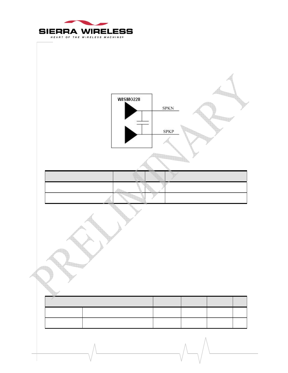
WA_DEV_W228_PTS_002 Rev 001 Page 56 of 108
Product Technical Specification &
Customer Design Guidelines
Speaker Features
Thespeaker,SPK,caneitherhaveasingle‐endedoradifferentialconnection.However,itisstrongly
recommendedtouseadifferentialconnectioninsteadofasingle‐endedconnectioninordertoreject
commonmodenoiseandTDMAnoise.Moreover,inasingle‐endedconnection,half(½)ofthe
powerislost.
Figure 18. Equivalent Circuit of SPK
Table 19. Speaker Details
Parameters Typical Unit Connection
Z (SPKP, SPKN) 16 or 32 Ω Differential
Z (SPKP, SPKN) 8 Ω Single-ended
Ifasingle‐endedconnectionisused,onlySPKPhastobeconnected.Theresultisamaximaloutput
powerdividedby2.Also,whenusingasingle‐endedconnection,besuretohaveaverygood
groundplane,verygoodfilteringaswellasshieldinginordertoavoidanydisturbanceontheaudio
path.
Electrical Characteristics
Thefollowingtabledescribestheelectricalcharacteristicsofthemicrophoneinterface,MIC.Note
thatthemaximumvaluesspecifiedinthefollowingtableareavailablewiththemaximumpower
outputconfigurationvaluessetbyanATcommand;butusingthetypicalvaluesisrecommended.
Table 20. Electrical Characteristics of SPK
Parameters Minimum Typical Maximum Unit
Biasing voltage SPKP and SPKN - 1.4 - V
Output swing RL=8Ω: AT+VGR=6*; single ended - - 1 Vpp
WA_DEV_W228_PTS_002 Rev 001 Page 57 of 108
Product Technical Specification &
Customer Design Guidelines
Parameters Minimum Typical Maximum Unit
voltage RL=8Ω: AT+VGR=6*; differential - - 2 Vpp
RL=16Ω or 32Ω: AT+VGR=6*; single
ended - - 1.1 Vpp
RL=16Ω or 32Ω: AT+VGR=6*;
differential - - 2.2 Vpp
RL Load resistance 6 8 -
Ω
IOUT Output current; peak value; RL=8Ω - - 90 mA
POUT RL=8Ω; AT+VGR=10*; - - 65 mW
* The output voltage depends on the output speaker gain set by the AT command. Refer to the WISMO218 AT
Commands Manual for more information about configuring AT commands.
Pin Description
Thefollowingtableprovidesthepindescriptionoftheanalogaudiointerface.
Table 21. Analog Audio Interface Pin Description
Pin # Signal I/O I/O Type Description
1 SPKP O Analog Speaker positive output
2 SPKN O Analog Speaker negative output
3 MICP I Analog Microphone positive input
4 MICN I Analog Microphone negative input
Application
Microphone
Thefollowingsub‐sectionsdescribethedifferentmicrophoneconfigurationexamples.
Differential Connection
WhenadifferentialconnectionofMICisused,itisnecessarytoadda2.2KΩresistorfromMICNto
GNDinordertohaveaproperbiasofthemicrophone.
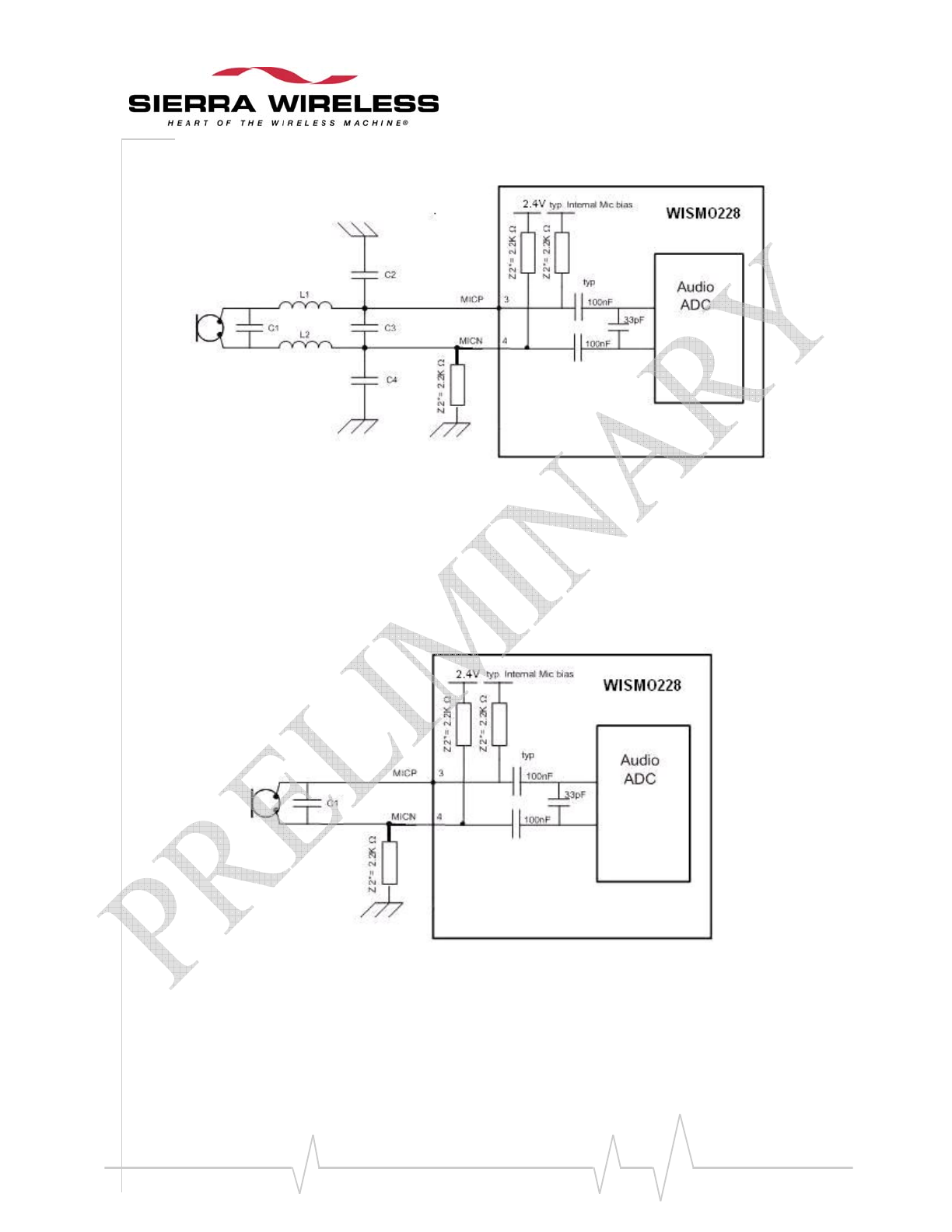
WA_DEV_W228_PTS_002 Rev 001 Page 58 of 108
Product Technical Specification &
Customer Design Guidelines
Figure 19. Example of a Differential MIC Connection with an LC Filter
AudioqualitycanbeverygoodwithoutL1,L2,C2,C3andC4dependingonthedesign.Butifthere
isEMIperturbation,thisfiltercanreducetheTDMAnoise.Thisfilter(L1,L2,C2,C3andC4)isnot
mandatory,andifnotused,thecapacitormustberemovedandthecoilreplacedbya0Ωresistoras
showninthefollowingschematic.
Figure 20. Example of a Differential MIC Connection without an LC Filter
ThecapacitorC1ishighlyrecommendedtoeliminateTDMAnoiseandmustbeclosetothe
microphone.
ThefollowingtableliststherecommendedcomponentstouseinimplementingadifferentialMIC
connectionwithoutanLCfilter.
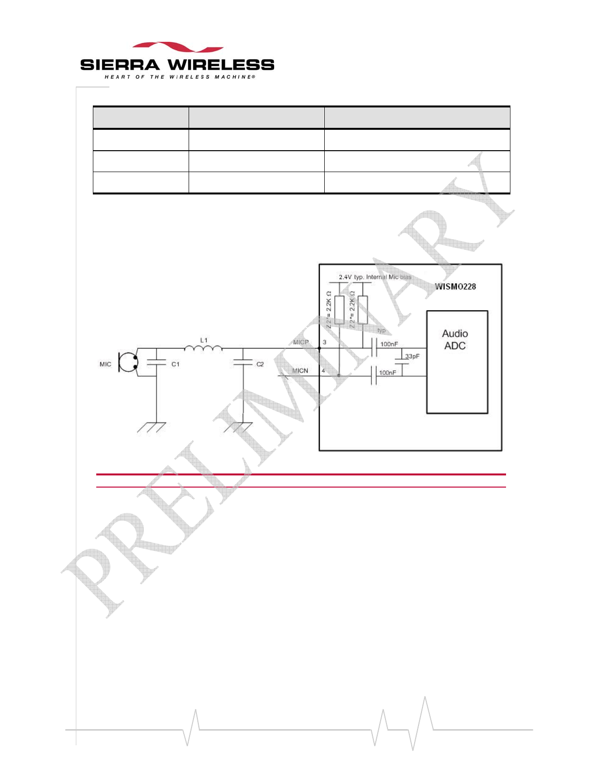
WA_DEV_W228_PTS_002 Rev 001 Page 59 of 108
Product Technical Specification &
Customer Design Guidelines
Component Description/Details Notes
C1 12pF to 33pF needs to be tuned depending on the design
C2, C3, C4 47pF needs to be tuned depending on the design
L1, L2 100nH needs to be tuned depending on the design
Single-Ended Connection
Whensingle‐endedconnectionisusedforMIC,MICNisjustleftopen.
Figure 21. Example of a Single-Ended MIC Connection with an LC filter
Note: Z2 is from 200Hz to 4kHz. For more details, refer to Table 18 Electrical Characteristics of MIC.
Whenusingasingle‐endedconnection,bearinmindthat:
• Theinternalinputimpedancevaluebecomes1100Ω,duetotheconnectionoftheotherend
toground.
• ThesingleendeddesignisverysensitivetoTDMAnoise.
• AverygoodgroundingontheMICisamustinordertoensuregoodaudioperformance
againstTDMA.Also,specialcareonthePCBlayoutmustbetaken.
• ItisrecommendedtoaddL1andC2footprintsasanLCfiltertotrytoeliminateTDMA
noise.
• Whennotused,thefiltercanberemovedbyreplacingL1witha0Ωresistorandby
disconnectingC2,asshowninthefollowingschematic.
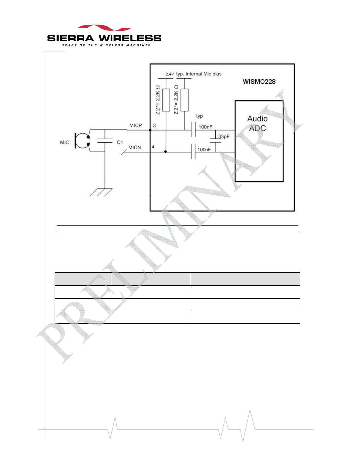
WA_DEV_W228_PTS_002 Rev 001 Page 60 of 108
Product Technical Specification &
Customer Design Guidelines
Figure 22. Example of a Single-Ended MIC Connection without an LC Filter
Note: *Z2 is from 200Hz to 4kHz. For more details, refer to Table 18 Electrical Characteristics of MIC.
ThecapacitorC1ishighlyrecommendedtoeliminateTDMAnoiseandmustbeclosetothe
microphone.
Thefollowingtableliststherecommendedcomponentstouseinimplementingasingle‐endedMIC
connectionwithoutanLCfilter.
Component Description/Details Notes
C1 12pF to 33pF needs to be tuned depending on the design
C2 needs to be tuned depending on the design
L1 needs to be tuned depending on the design
Speaker SPKP ad SPKN
Differential Connection
Inadifferentialconnection,simplyconnectbothSPKPandSPKNtothespeaker.
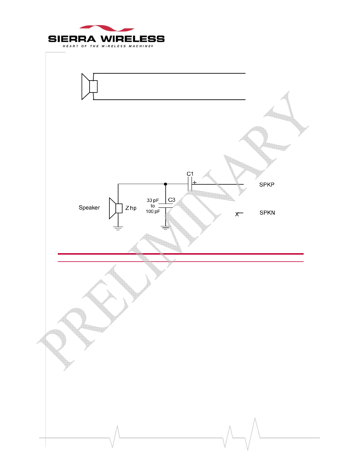
WA_DEV_W228_PTS_002 Rev 001 Page 61 of 108
Product Technical Specification &
Customer Design Guidelines
SPKP
SPKN
Figure 23. Example of a Differential Speaker Connection
Single-Ended Connection
Inasingle‐endedconnection,SPKNcanbeleftopen.Refertothefollowingdiagramforatypical
single‐endedimplementation.
Figure 24. Example of a Single-Ended Speaker Connection
Note: 4.7µF < C1 < 47 µF (Depending on speaker characteristics and output power.)
Whenusingasingle‐endedconnection,bearinmindthat:
• Usingasingle‐endedconnectionincludeslosingoutputpower(‐6dB)ascomparedtoa
differentialconnection.
• TheconnectionbetweentheWISMO228pinsandthespeakermustbedesignedtokeepthe
serialimpedancelowerthan1.5Ω.
Design Recommendations
General
Whenbothspeakerandmicrophoneareexposedtotheexternalenvironment,itisrecommendedto
addESDprotectionasclosetothespeakerormicrophoneaspossible,connectedbetweentheaudio
linesandagoodground.
Whenusingthesingle‐endedconnectionofMICP,ensuretohaveagoodgroundplane,good
filteringaswellasshielding,inordertoavoidanydisturbanceontheaudiopath.
Itisalsoimportanttoselectanappropriatemicrophone,speakerandfilteringcomponentstoavoid
TDMAnoise.
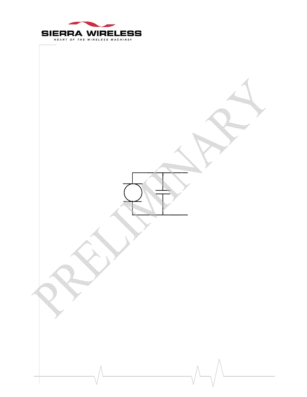
WA_DEV_W228_PTS_002 Rev 001 Page 62 of 108
Product Technical Specification &
Customer Design Guidelines
Recommended Microphone Characteristics
• Theimpedanceofthemicrophonehastobearound2KΩ
• Sensitivityisfrom‐40dBto‐50dB
• SNR>50dB
• FrequencyresponseiscompatiblewithGSMspecifications
TosuppressTDMAnoise,itishighlyrecommendedtousemicrophoneswithtwointernal
decouplingcapacitors:
• CM1=56pF(0402package)fortheTDMAnoisecomingfromthedemodulationofthe
GSM850/EGSM900frequencysignals
• CM2=15pF(0402package)fortheTDMAnoisecomingfromthedemodulationofthe
DCS1800/PCS1900frequencysignals
Thecapacitorshavetobesolderedinparalleltothemicrophoneasshowninthefigurebelow.
CM
Figure 25. Capacitor Soldered in Parallel to the Microphone
Recommended Speaker Characteristics
• Typeofspeakers:Electro‐magnetic/10mW
• Impedance:8Ωforhands‐free
• Impedance:32Ωforheadskit
• Sensitivity:110dBSPLmin
• ReceiverfrequencyresponseiscompatiblewithGSMspecifications.
Recommended Filtering Components
WhendesigningaGSMapplication,itisimportanttoselecttherightaudiofilteringcomponents.
Thestrongestnoise,calledTDMA,ismainlyduetothedemodulationoftheGSM850,EGSM900,
DCS1800andPCS1900signals,whereaburstisproducedevery4.615ms;andthefrequencyofthe
TDMAsignalisequalto216.7Hzplusharmonics.
TDMAnoisecanbesuppressedbyfilteringtheRFsignalusingtheappropriatedecoupling
components.
WA_DEV_W228_PTS_002 Rev 001 Page 63 of 108
Product Technical Specification &
Customer Design Guidelines
Thetypesoffilteringcomponentsare:
• RFdecouplinginductors
• RFdecouplingcapacitors
Agood“ChipS‐Parameter”simulatorisavailablefromMurata.Referto
http://www.murata.com/products/design_support/mcsil/index.htmlformoredetails.
UsingdifferentMuratacomponents,itcanbeseenthatdifferentpackages(withdifferentvaluesand
ratings)canhavedifferentcouplingeffects.Refertothefollowingtableforexamplesusingdifferent
Muratacomponents.
Package 0402
Filtered band GSM900 GSM850/900 DCS/PCS
Value 100nH 56pF 15pF
Types Inductor Capacitor Capacitor
Position Serial Shunt Shunt
Manufacturer Murata Murata Murata
Rated 150mA 50V 50V
Reference LQG15HSR10J02 or
LQG15HNR10J02 GRM1555C1H560JZ01 GRM1555C1H150JZ01 or
GRM1555C1H150JB01
Package 0603
Filtered band GSM900 GSM850/900 DCS/PCS
Value 100nH 47pF 10pF
Types Inductor Capacitor Capacitor
Position Serial Shunt Shunt
Manufacturer Murata Murata Murata
Rated 300mA 50V 50V
Reference LQG18HNR10J00 GRM1885C1H470JA01 or
GRM1885C1H470JB01 GRM1885C1H150JA01 or
GQM1885C1H150JB01
Audio Track and PCB Layout Recommendation
ToavoidTDMAnoise,itisrecommendedtosurroundtheaudiotrackswithgroundasshowninthe
followingfigure.
WA_DEV_W228_PTS_002 Rev 001 Page 64 of 108
Product Technical Specification &
Customer Design Guidelines
Figure 26. Audio Track Design
Fordifferentialconnections,itisnecessarytoadda2.2KΩresistorfromMICNtoGNDtohavea
properbiasofthemicrophone.
Figure 27. Differential Audio Connection
Forsingle‐endedconnections,thenegativepoleofthemicrophone,MICN,shouldbeconnectedto
GND.
Differential Audio line is
always in parallel
WA_DEV_W228_PTS_002 Rev 001 Page 65 of 108
Product Technical Specification &
Customer Design Guidelines
Figure 28. Single-Ended Audio Connection
Caution: It is a must to avoid digital tracks crossing under and over the audio tracks.
Even when MICP is singled-ended, it is highly recommended to have the MIC ground and the LC
filter ground to act as an audio analog ground during the PCB layout. This audio ground, together
with the MICP signal, should act as the differential line pair. And this audio ground should only be
connected to the WISMO228 module ground as close as possible to the castellation GND pin of the
WISMO228.
The same case is applicable to SPKP and SPKN.
Also, the audio interface is ESD sensitive. It is a must to add ESD protection to the interface once it
is externally accessible. The recommended ESD protection is the ESDA6VIL from ST.
WA_DEV_W228_PTS_002 Rev 001 Page 66 of 108
Product Technical Specification &
Customer Design Guidelines
Pulse-Width Modulators (PWMs)
TheWISMO228containstwoPulse‐WidthModulators(PWMs)thatcanbeusedinconjunctionwith
anexternaltransistorfordrivingavibrator,orabacklightLED.EachPWMusestwo7‐bitunsigned
binarynumbers:onefortheoutputperiodandoneforthepulsewidthorthedutycycle.
TherelativetimingforthePWMoutputisshowninthefigurebelow.
Figure 29. Relative Timing for the PWM Output
Electrical Characteristics
ThefollowingtabledescribestheelectricalcharacteristicsofthePWMinterface.
Table 22. Electrical Characteristics of the PWM Interface
Parameters Conditions Minimum Typical Maximum Unit
VOH
High impedance load 2.7 2.85 - V
Load with IoH = 4mA - 2.4 - V
VOL - - - 0.1 V
IPEAK - - - 4 mA
Frequency - 25.6 - 1083.3 kHz
Duty cycle - 0* - 100* %
Pin Description
ThefollowingtableprovidesthepindescriptionofthePulse‐WidthModulators.
Table 23. PWM Pin Description
Pin # Signal I/O I/O Type Description
35 PWM1 O 2V8 PWM output
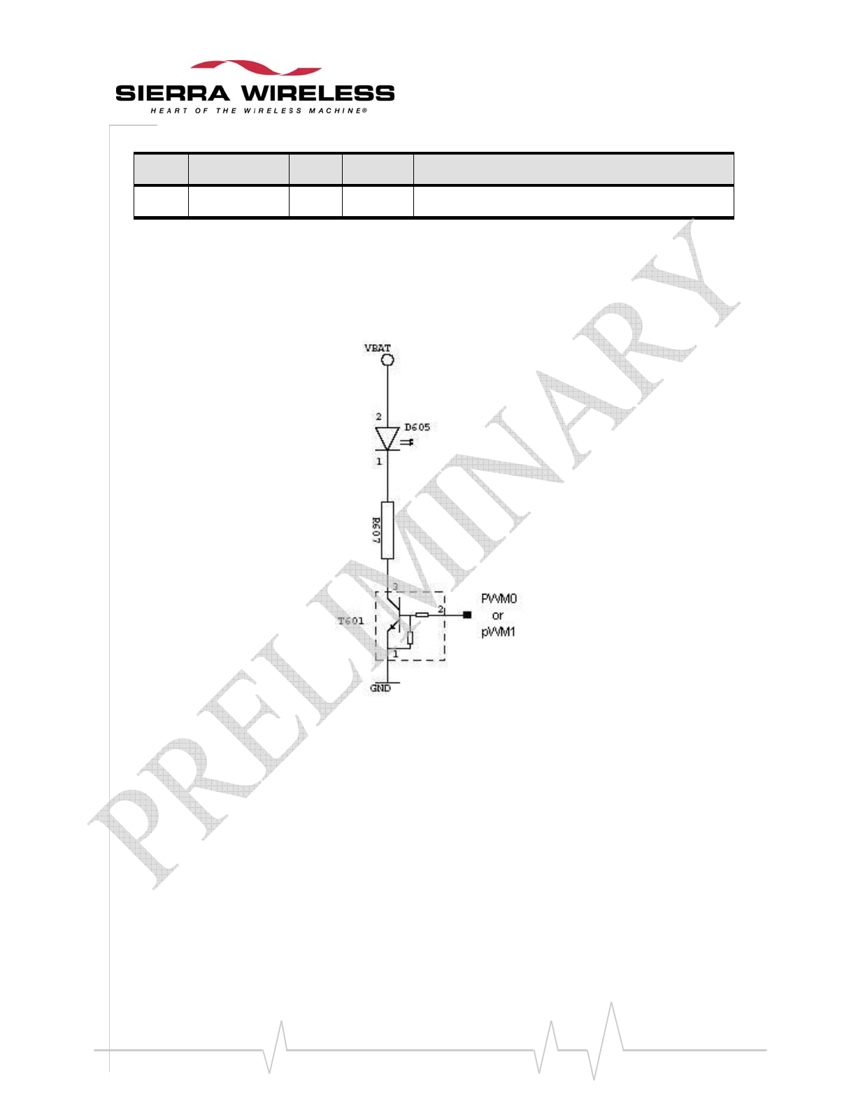
WA_DEV_W228_PTS_002 Rev 001 Page 67 of 108
Product Technical Specification &
Customer Design Guidelines
Pin # Signal I/O I/O Type Description
36 PWM0 O 2V8 PWM output
Application
BoththePWM0andPWM1signalscanbeusedinconjunctionwithanexternaltransistorfordriving
avibrator,orabacklightLED.
Figure 30. Example of an LED Driven by the PWM0 or PWM1 Output
ThevalueofR607canbeharmonizeddependingontheLED(D605)characteristics.
TherecommendeddigitaltransistortouseforT601istheDTC144EEfromROHM.
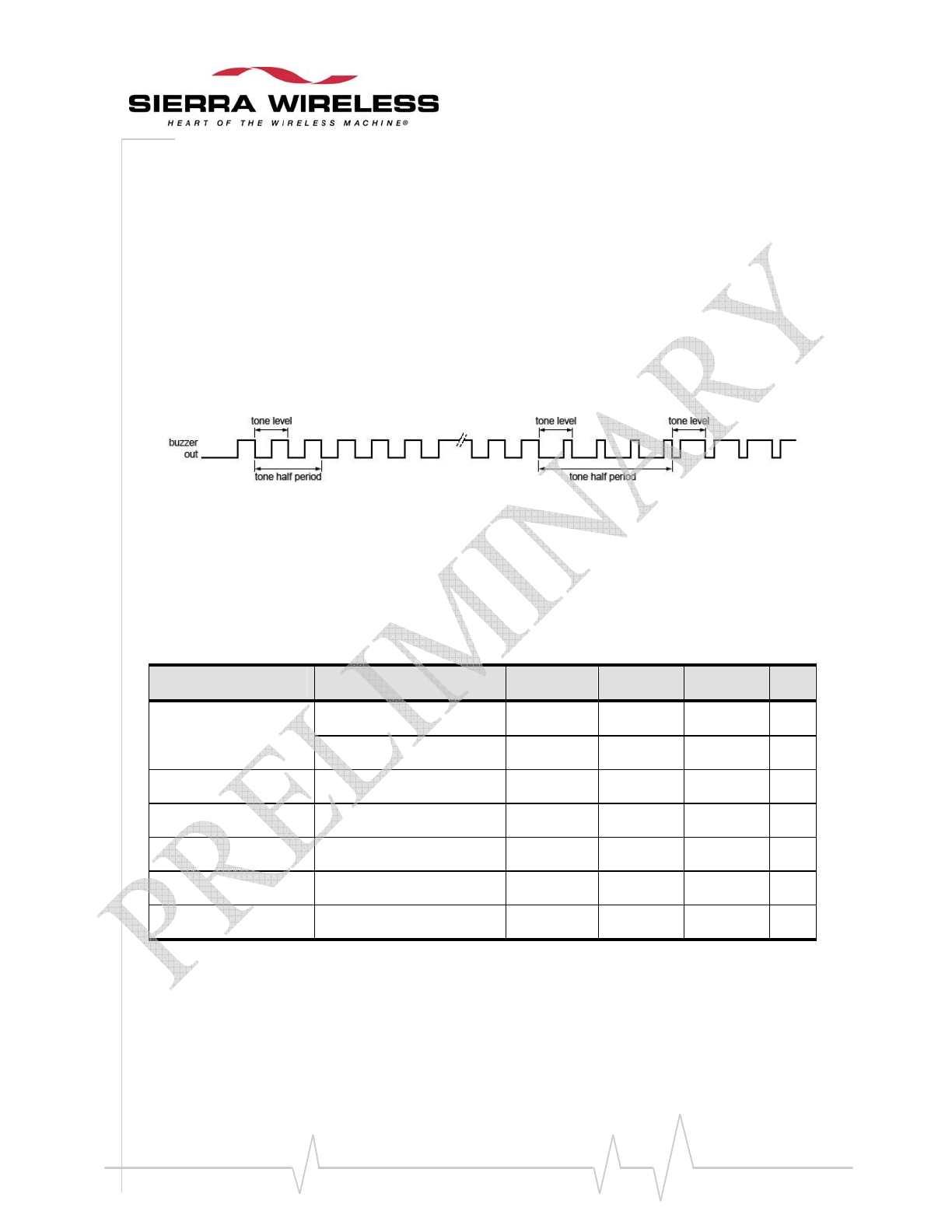
WA_DEV_W228_PTS_002 Rev 001 Page 68 of 108
Product Technical Specification &
Customer Design Guidelines
BUZZER Output
TheBUZZERsignalcanbeusedinconjunctionwithanexternaltransistor/MOSFETfordrivinga
buzzerinordertogiveamaximumcurrentof100mA(PEAK)andanaverageof40mA,depending
onapplicationrequirement.
Itoutputsasquarewaveatthedesiredtonefrequency.Thetonefrequenciesareprogrammableand
canbere‐programmedon‐the‐flytogeneratemonophonicaudioringtonesoralerttones.Thetone
levelcanalsobeadjustedin4dBsteps,ormuted.
Figure 31. BUZZER Output
Electrical Characteristics
ThefollowingtabledescribestheelectricalcharacteristicsoftheBUZZERsignal.
Table 24. Electrical Characteristics of the BUZZER Signal
Parameters Conditions Minimum Typical Maximum Unit
VOH
High impedance load 2.7 2.85 - V
Load with IoH = 4mA - 2.4 - V
IPEAK - - - 4 mA
VOL - - - 0.1 V
Frequency - 200 - 2500 Hz
Duty cycle - 0* - 100* %
Tone level 4 dB step -24 - 0 dB
* Be mindful of the maximum frequency and the minimum/maximum duty cycle. There is a limitation to these
parameters due to the RC environment. The amplitude modulation becomes less fine when the set limits are
reached.
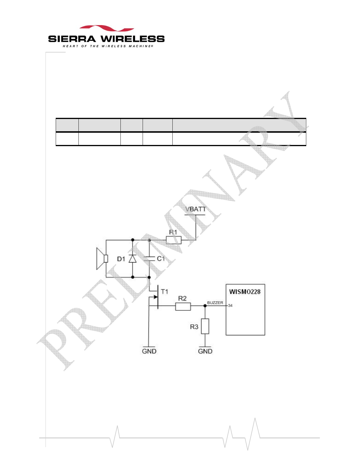
WA_DEV_W228_PTS_002 Rev 001 Page 69 of 108
Product Technical Specification &
Customer Design Guidelines
Pin Description
ThefollowingtableprovidesthepindescriptionoftheBUZZERsignal.
Table 25. BUZZER Pin Description
Pin # Signal I/O I/O Type Description
34 BUZZER O 2.8V Buzzer output
Application
Themaximumpeakcurrentofthetransistor/MOSFETis100mAandthemaximumaveragecurrent
is40mA,whilethepeakcurrentoftheBUZZERpinshouldbelessthan4mA.Atransientvoltage
suppressordiodemustbeaddedasshownbelow.
Figure 32. Example of a BUZZER Implementation
Where:
• R1mustbechoseninordertolimitthecurrentatI
PEAK
maxto100mAandmustbeadjusted
inrelationtothefrequencyandthedutycycleused.
• D1=BAV70T‐7orBAS16(forexample)

WA_DEV_W228_PTS_002 Rev 001 Page 70 of 108
Product Technical Specification &
Customer Design Guidelines
• T1=FDN335N(forexample)
• R2=0Ω
• R3=1MΩ
Note: A low filter is recommended at low frequencies.
Low Filter Calculations
Tocomputeforthecut‐offfrequency,usetheformulaFc=1/(2*Π*Req*C1)where:
• Fc=cut‐offfrequency
• Req=thetotalresistorsinline
• C1=thecapacitivechargeonT1andtheground
Bearinmindthat:
• FcmustbehigherthanFBUZZ‐OUT
• Fcmustbeatleast64*FBUZZ‐OUT
Note: The frequency modulation of the BUZZER signal is 64*FBUZZ-OUT.
Recommended Characteristics
• Electro‐magnetictype
• Impedance:7to30Ω
• Sensitivity:90dBSPLmin@10cm
• Current:60to90mA
TheBUZZERoutputcanalsobeusedtodriveanLEDasshowninthefigurebelow.
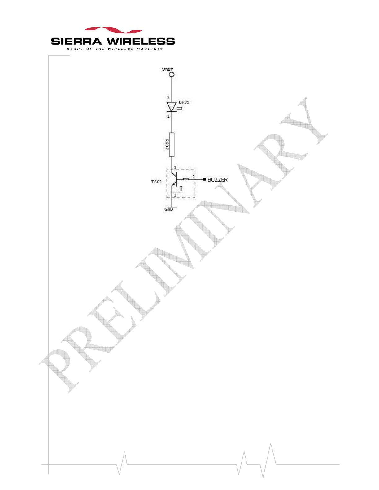
WA_DEV_W228_PTS_002 Rev 001 Page 71 of 108
Product Technical Specification &
Customer Design Guidelines
Figure 33. Example of an LED Driven by the BUZZER Output
ThevalueofR607canbeharmonizeddependingontheLED(D605)characteristics.
TherecommendeddigitaltransistortouseforT601istheDTC144EEfromROHM.
WA_DEV_W228_PTS_002 Rev 001 Page 72 of 108
Product Technical Specification &
Customer Design Guidelines
ON/~OFF Signal
TheON/~OFFpinisusedtoswitchONorswitchOFFtheWISMO228.Itisinternallyconnectedto
thepermanent3.0VsupplyregulatorinsidetheWISMO228viaapull‐upresistor.Oncethereis
VBATTsupplytotheWISMO228,this3.0VsupplyregulatorwillbeenabledandsotheON/~OFF
signalisbydefaultatHIGHlevel.
ALOWlevelsignalhastobeprovidedontheON/~OFFpintoswitchtheWISMO228ON.
Caution: All external signals must be inactive when the WISMO228 is OFF to avoid any damage when starting
and to allow the WISMO228 to start and stop correctly.
Electrical Characteristics
ThefollowingtabledescribestheelectricalcharacteristicsoftheON/~OFFsignal.
Table 26. Electrical Characteristics of the ON/~OFF Signal
Parameter I/O Type Minimum Typical Maximum Unit
VIH 2V8 2.4 - 3.0 V
VIL 2V8 - - 0.4 V
Pin Description
ThefollowingtableprovidesthepindescriptionoftheON/~OFFsignal.
Table 27. ON/~OFF Signal Pin Description
Pin # Signal I/O I/O Type Description
37 ON/~OFF I 2V8 WISMO228 Power ON/OFF
WA_DEV_W228_PTS_002 Rev 001 Page 73 of 108
Product Technical Specification &
Customer Design Guidelines
Application
Figure 34. Example of the ON/~OFF Pin Connection
Power ON
Figure 35. Power-ON Sequence
Table 28. Power-ON Sequence
Minimum (s) Typical (s) Maximum (s)
Tready 4 5 7
TheON/~OFFsignallevelisdetectedabout250msafterVBATTisavailable.
Note: This timing might be temperature dependant.
WA_DEV_W228_PTS_002 Rev 001 Page 74 of 108
Product Technical Specification &
Customer Design Guidelines
ThevoltageofthissignalhastobepulledLOWforatleast685msforpoweringON.Withinthis
685ms,theWISMO_READYsignalwillinitiallysettoHIGHforabout135msandthenresumeto
LOW.
DuringthepowerONsequence,aninternalresetisautomaticallyperformedfor38ms(typically).
Duringthisphase,anyexternalresetshouldbeavoided.
OncetheWISMO228isproperlypoweredON,theWISMO_READYpinwillsettoHIGHlevelto
acknowledgethesuccessfulpoweringONoftheWISMO228beforeitisreadytooperate.The
ON/~OFFsignalcanbeleftatLOWleveluntilpoweroff.
TherecommendedwaytoreleasetheON/~OFFsignalistodetecttheWISMO_READYsignal
within685msofpoweringONwhilethelevelpulseoftheON/~OFFsignalissettoLOW,andwait
untiltheWISMO_READYsignalgoesHIGHagain.
Power OFF
TheWISMO228canbepoweredoffbyeithersoftwareorhardware.Refertothefollowingdiagram
forthepowerOFFsequence.
Figure 36. Power-OFF Sequence

WA_DEV_W228_PTS_002 Rev 001 Page 75 of 108
Product Technical Specification &
Customer Design Guidelines
Software Power OFF
TheATcommandAT+CPOFisusedtopowerOFFtheWISMO228.
Note: If the ON/~OFF pin is maintained at LOW level when AT+CPOF is used, the module cannot be
switched OFF.
Hardware Power OFF
ALOWlevelpulseisappliedontheON/~OFFpinforTBCseconds.AT+CPOFwillthenbe
automaticallysenttotheWISMO228.
OncetheWISMO228receivestheAT+CPOFcommand,theWISMO228willbeunregisteredfrom
thenetwork.TheWISMO_READYpinwillbecomeLOWtoindicatethatATcommandsareno
longeravailablefortheWISMO228.IftheON/~OFFsignalisHIGH,thentheWISMO228willalso
beswitchedOFF.
WA_DEV_W228_PTS_002 Rev 001 Page 76 of 108
Product Technical Specification &
Customer Design Guidelines
WISMO_READY Indication
ThissignalindicatesthestatusoftheWISMO228afterbeingpoweredON.Notethatthereisan
initialpositivepulseoflessthan200msduringpowerON.RefertoFigure35:Power‐ONSequence
formoreinformationregardingthepowerONsequence.OncetheWISMO228isproperlypowered
ON,theWISMO_READYsignalwillsettoHIGHtoacknowledgethesuccessfulpoweringONof
theWISMO228beforeitisreadytooperate.Likewise,thepinwillsettoLOWbeforepoweringOFF.
Electrical Characteristics
ThefollowingtabledescribestheelectricalcharacteristicsoftheWISMO_READYsignal.
Table 29. Electrical Characteristics of the WISMO_READY Indication
Parameters I/O Type Minimum Typical Maximum Unit
VOH 2V8 2.7 2.8 2.95 V
VOL 2V8 - - 0.4 V
Pin Description
ThefollowingtableprovidesthepindescriptionoftheWISMO_READYsignal.
Table 30. WISMO_READY Indication Pin Description
Pin # Signal I/O I/O Type Description
7 WISMO_READY O 2V8 WISMO228 ready indication
WA_DEV_W228_PTS_002 Rev 001 Page 77 of 108
Product Technical Specification &
Customer Design Guidelines
VCC_2V8 Output
TheVCC_2V8outputvoltagesupplyisavailablewhentheWISMO228isswitchedONandcanonly
beusedforpull‐upresistor(s)andasareferencesupply.
Electrical Characteristics
ThefollowingtabledescribestheelectricalcharacteristicsoftheVCC_2V8signal.
Table 31. Electrical Characteristics of the VCC_2V8 Signal
Parameters Minimum Typical Maximum Unit
VCC_2V8
Output voltage 2.70 2.80 2.95 V
Output Current
Full-power mode - - 50 mA
Sleep mode - - 3 mA
Pin Description
ThefollowingtableprovidesthepindescriptionoftheVCC_2V8voltagesupply.
Table 32. VCC_2V8 Pin Description
Pin # Signal I/O I/O Type Description
46 VCC_2V8 O Supply Digital supply
Application
Thisdigitalpowersupplyismainlyusedto:
• Pull‐upsignalssuchasI/Os
• SupplythedigitaltransistorsdrivingLEDs
• ActasavoltagereferencefortheADCinterfaceAUX‐ADC0
WA_DEV_W228_PTS_002 Rev 001 Page 78 of 108
Product Technical Specification &
Customer Design Guidelines
BAT-RTC (Backup Battery)
TheBAT‐RTC(backupbattery)pinisusedasaback‐uppowersupplyfortheinternalRealTime
Clock(RTC).VBATTprovidesthepowersupplytotheRTCwhenVBATTisswitchedonbuta
back‐uppowersupplyisneededtosavethedateandhourwhenitisswitchedoff.
IfVBATTisavailable,theback‐upbatterycanbechargedbytheinternal3.0Vpowersupply
regulatorviaa2KΩresistorimplementedinsidetheWISMO228.
IftheRTCisnotused,thispincanbeleftopen.
Electrical Characteristics
ThefollowingtabledescribestheelectricalcharacteristicsoftheBAT‐RTCsignal.
Table 33. Electrical Characteristics of the BAT-RTC Signal
Parameters Minimum Typical Maximum Unit
Input voltage - 3.0 - V
Input current consumption* - 2.5 - µA
Output voltage 2.82 3.0 3.18 V
Max charging current (@VBATT=3.6V) - 0.6 - mA
* Provided by an RTC back-up battery when the WISMO228 is off and VBATT = 0V.
Pin Description
ThefollowingtableprovidesthepindescriptionoftheBAT‐RTCvoltagesupply.
Table 34. BAT-RTC Pin Description
Pin # Signal I/O I/O Type Description
6 BAT-RTC I/O Supply RTC Back-up supply
Application
Thebackuppowersupplycanbeanyofthefollowing:
• Asupercapacitor
WA_DEV_W228_PTS_002 Rev 001 Page 79 of 108
Product Technical Specification &
Customer Design Guidelines
• Anonrechargeablebattery
• Arechargeablebatterycell
Super Capacitor
Figure 37. RTC Supplied by a Gold Capacitor
Estimatedsupplytimewitha0.47Fgoldcapacitor:25minutes(minimum).
Note: The maximum voltage of the gold capacitor is 3.9V.
Non-Rechargeable Battery
Figure 38. RTC Supplied by a Non Rechargeable Battery
Thediode,D1,ismandatorytopreventthenonrechargeablebatteryfrombeingdamaged.
Estimatedsupplytimewithan85mAhbattery:800hours(minimum).
WA_DEV_W228_PTS_002 Rev 001 Page 80 of 108
Product Technical Specification &
Customer Design Guidelines
Rechargeable Battery Cell
Figure 39. RTC Supplied by a Rechargeable Battery Cell
Estimatedsupplytimewithafullycharged3.4mAhrechargeablebattery:7days(minimum).
Caution: Before battery cell assembly, ensure that the cell voltage is lower than 3.0V to avoid damaging the
WISMO228.
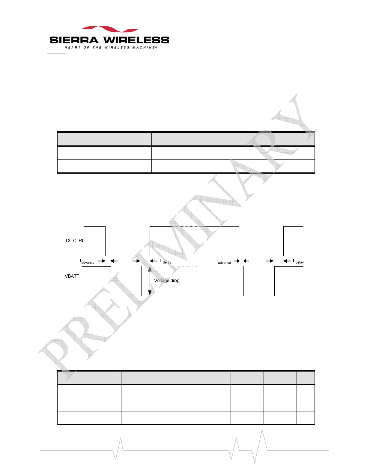
WA_DEV_W228_PTS_002 Rev 001 Page 81 of 108
Product Technical Specification &
Customer Design Guidelines
TX_CTRL Signal for TX Burst Indication
TheTX_CTRLsignalisa2.8VindicationsignalforTXBurstwitha100KΩpull‐upresistor
implementedinsidetheWISMO228module.
Table 35. TX_CTRL Status
WISMO228 State TX_CTRL Status
During TX burst Low
No TX High
DuringTXburst,therewillbehighercurrentdrainfromtheVBATTpowersupplywhichcausesa
voltagedrop.ThisvoltagedropfromVBATTisagoodindicationofahighcurrentdrainsituation
duringTXburst.
Figure 40. TX_CTRL State During TX Burst
Electrical Characteristics
ThefollowingtabledescribestheelectricalcharacteristicsoftheTX_CTRLsignal.
Table 36. Electrical Characteristics of the TX_CTRL Signal
Parameters Conditions Minimum Typical Maximum Unit
VOH 2.6 - 2.95 V
VOL - - 0.4 V
Tadvance @500mA - 18 - µs
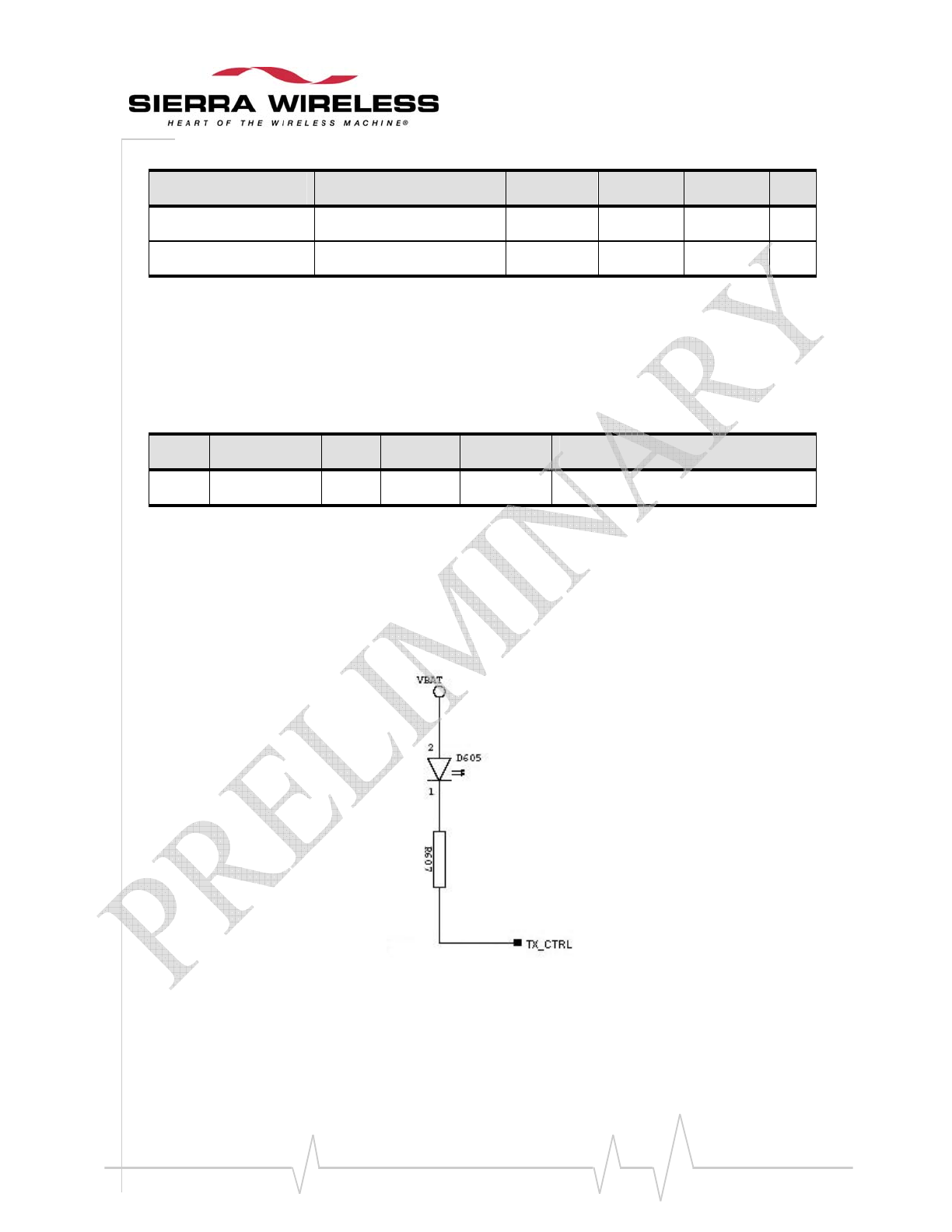
WA_DEV_W228_PTS_002 Rev 001 Page 82 of 108
Product Technical Specification &
Customer Design Guidelines
Parameters Conditions Minimum Typical Maximum Unit
@1A - 27 - µs
Tdelay - 11 - µs
Pin Description
ThefollowingtableprovidesthepindescriptionoftheTX_CTRLsignal.
Table 37. TX_CTRL Signal Pin Description
Pin # Signal I/O I/O Type Reset State Description
18 TX_CTRL O 2V8 1 TX Burst indication
Application
TheTXburstindicationsignal,TX_CTRL,canbeusedtodriveanLEDthroughatransistor.Itcan
beagoodvisualindicatorforanyTXactivities.
Figure 41. Example of a TX Status Implementation
ThevalueofR607canbeharmonizeddependingontheLED(D1)characteristics.
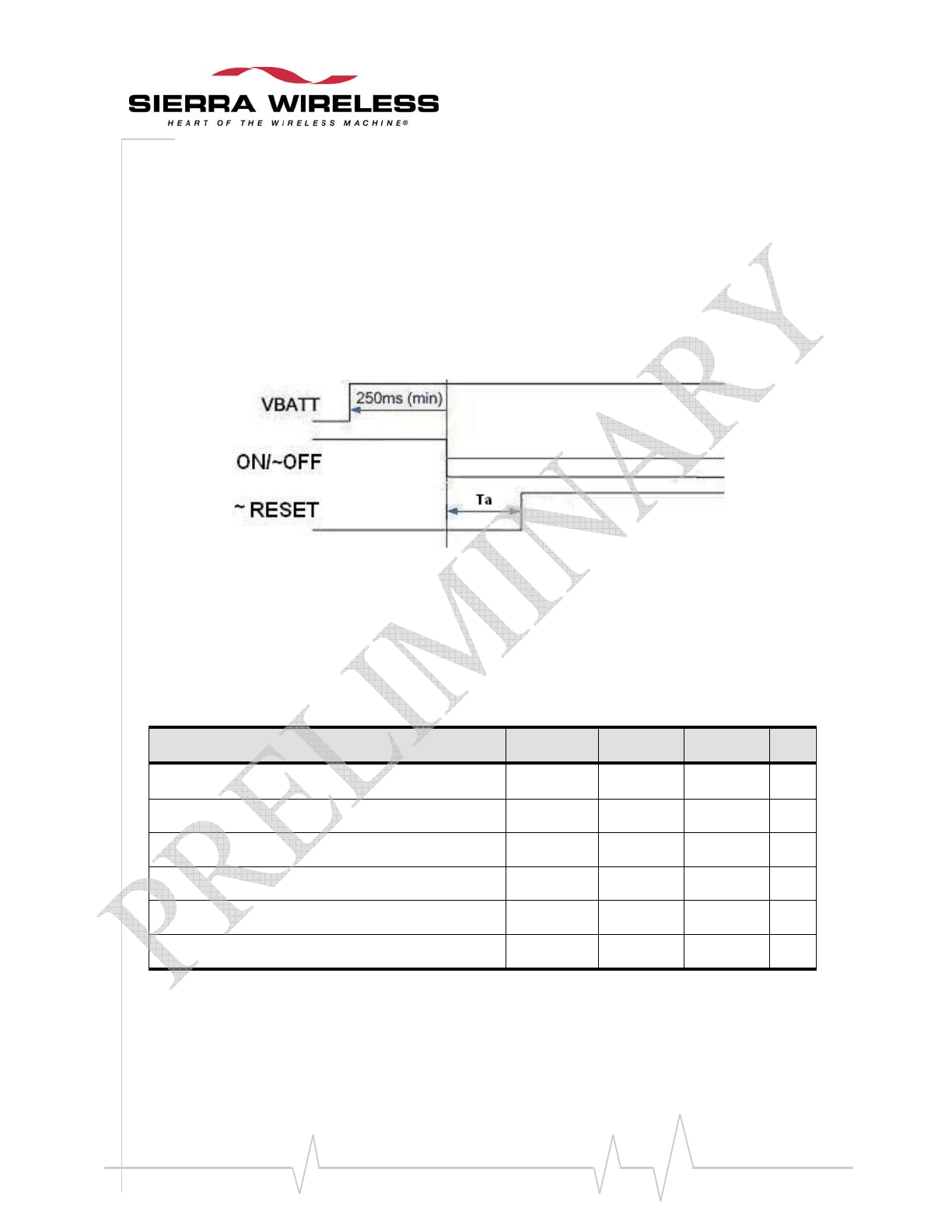
WA_DEV_W228_PTS_002 Rev 001 Page 83 of 108
Product Technical Specification &
Customer Design Guidelines
Reset
The~RESETpinisahardwareresetandshouldonlybeusedforemergencyresets.Ithasa100KΩ
internalpullupresistortoVCC_2V8.
Toactivatethe«emergency»resetsequence,the~RESETsignalhastobesettoLOWlevelmanually.
Thiscanbedonebyusingapushbutton,forexample.
Figure 42. Reset Timing
Electrical Characteristics
Thefollowingtabledescribestheelectricalcharacteristicsofthe~RESETsignal.
Table 38. Electrical Characteristics of the Reset Signal
Parameters Minimum Typical Maximum Unit
Input Impedance ( R )* - 100K - Ω
Input Impedance (C) - 10nF F
Cancellation time (Ta) at power up only - 38 - ms
VH** 1.57 - - V
VIL - 0 1.2 V
VIH 1.96 2.8 -- V
* Internal pull up resistance
** VH : Hysterisis Voltage
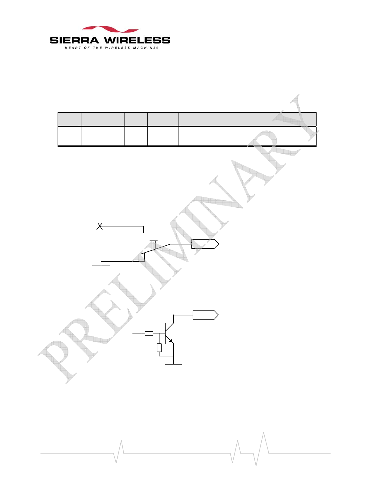
WA_DEV_W228_PTS_002 Rev 001 Page 84 of 108
Product Technical Specification &
Customer Design Guidelines
Pin Description
ThefollowingtableprovidesthepindescriptionoftheRESETsignal.
Table 39. Reset Pin Description
Pin # Signal I/O I/O Type Description
12 ~RESET 100K
Pull-up 2V8 WISMO228 Reset
Application
Ifthe«emergency»resetisused,ithastobedrivenbyeitherapushbuttonoranopen
collector/draintransistorasshowninthefiguresbelow.
GND
1
2
3
Push button
~RESET
Figure 43. Example of ~RESET Pin Connection with a Push Button Configuration
GND
~RESET
Reset
command T1
Rohm DTC144EE
Figure 44. Example of ~RESET Pin Connection with a Transistor Configuration
Anopencollectororopendraintransistorcanalsobeusedtodrivethe~RESETpin(duetothe
internalpull‐upresistorembeddedintotheWISMO228).Ifanopencollectorischosen,the
recommendeddigitaltransistortouseforT1istheDTC144EEfromROHM.
WA_DEV_W228_PTS_002 Rev 001 Page 85 of 108
Product Technical Specification &
Customer Design Guidelines
Table 40. Reset Commands
Reset Command ~RESET Operating Mode
1 0 Reset activated
0 1 Reset inactive
Note: It is recommended to add a varistor (such as the AVL5M02200 from AMOTECH) on the ~RESET pin
in order to enhance ESD immunity.
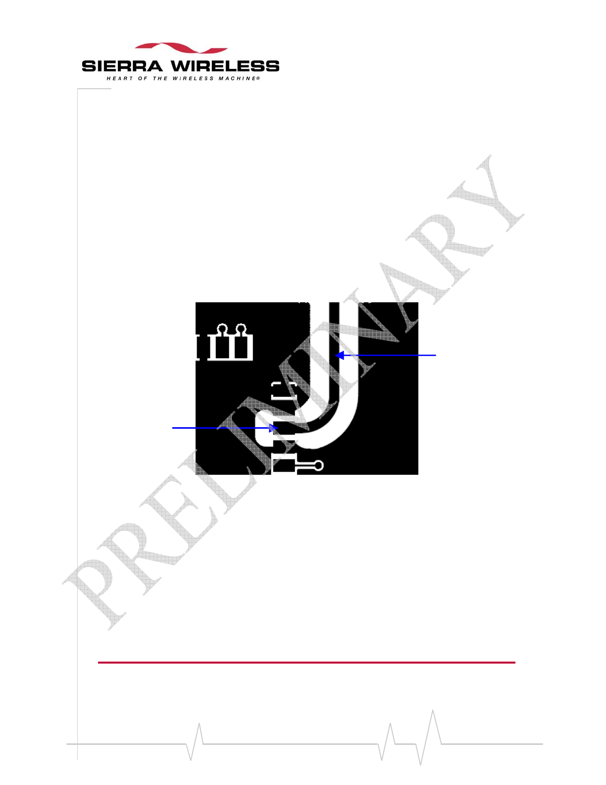
WA_DEV_W228_PTS_002 Rev 001 Page 86 of 108
Product Technical Specification &
Customer Design Guidelines
RF Interface
TheRFinterfaceallowsthetransmissionofradiofrequency(RF)signalsfromtheWISMO228toan
externalantenna.Thisinterfacehasanominalimpedanceof50ΩandaDCresistanceof0Ω.
RF Connection
TheRFinput/outputoftheWISMO228isthroughoneofthecastellationpins(Pin21,ANT),with
groundedcastellationpinsatbothsides.Thiscastellationpinmustbeconnectedtoa50ΩRFlinein
ordertoprotecttheantennalinefromthenoisecomingfrombasebandsignals.
Figure 45. Example of a 50
Ω
RF Line
The50ΩRFlineissurroundedbytwogroundplanesinordertoprotecttheantennalinefrom
noise.Thelengthofthelineshouldn’tbetoolong(nomorethanafewcentimeters)becauseofRF
insertionloss.Thewidthofthelinemustbecalculatedinordertoensurea50Ωcharacteristic
impedance.
Forthissamereason,theembeddedRFlineshouldlikewisebekeptabout1cmawayfromany
(noisy)basebandsignalinordertoensureagoodRXsensitivitylevel.
Theotherendofthe50ΩRFlinecanbeconnectedtoanRFconnectorortoasolderingpadinorder
toconnectanantenna.ItisalsopossibletouseanantennachiportodesignaPCBantennadirectly
ontheapplicationboard.
TheANTpinoftheWISMO228isESDprotectedforboth±4KVcontactand±8KVairdischarge.
Note: The correct antenna cable and connector should be chosen in order to minimize loss in the frequency
bands used for GSM800, EGSM900, DCS1800 and PCS1900.
Castellation pin
for ANT
50Ω RF line
WA_DEV_W228_PTS_002 Rev 001 Page 87 of 108
Product Technical Specification &
Customer Design Guidelines
0.5dB can be considered as the maximum value for loss between the WISMO228 and an external
connector.
RF Performances
RFperformancesarecompliantwithETSIrecommendationGSM05.05.Listedbelowarethemain
parametersforboththeReceiverandtheTransmitter.
ThemainparametersfortheReceiverare:
• GSM850/EGSM900ReferenceSensitivity=‐108dBm(typ.)
• DCS1800/PCS1900ReferenceSensitivity=‐108dBm(typ.)
• Selectivity@200kHz:>+9dBc
• Selectivity@400kHz:>+41dBc
• Lineardynamicrange:63dB
• Co‐channelrejection:>=9dBc
ThemainparametersfortheTransmitterare:
• Maximumoutputpower(EGSM):33dBm+/‐2dBatambienttemperature
• Maximumoutputpower(GSM1800):30dBm+/‐2dBatambienttemperature
• Minimumoutputpower(EGSM):5dBm+/‐5dBatambienttemperature
• Minimumoutputpower(GSM1800):0dBm+/‐5dBatambienttemperature
Antenna Specifications
Theoptimumoperatingfrequencydependsontheapplication.Adual‐bandoraquad‐bandantenna
willworkinthefollowingfrequencybandsandshouldhavethefollowingcharacteristics.
Table 41. Antenna Specifications
Characteristic WISMO228
GSM 850 E-GSM 900 DCS 1800 PCS 1900
TX Frequency 824 to 849 MHz 880 to 915 MHz 1710 to 1785 MHz 1850 to 1910 MHz
RX Frequency 869 to 894 MHz 925 to 960 MHz 1805 to 1880 MHz 1930 to 1990 MHz
Impedance 50Ω
VSWR
Rx max 1.5 :1
Tx max 1.5 :1

WA_DEV_W228_PTS_002 Rev 001 Page 88 of 108
Product Technical Specification &
Customer Design Guidelines
Characteristic WISMO228
Typical radiated gain 0dBi in one direction at least
Caution: Both mechanical and electrical antenna adaptations are key issues in the design of a GSM terminal.
It is strongly recommended to work with an antenna manufacturer to either develop an antenna
adapted to the application or to adapt an existing solution to the application.

WA_DEV_W228_PTS_002 Rev 001 Page 89 of 108
Product Technical Specification &
Customer Design Guidelines
5. Consumption Measurement
Procedure
ThischapterdescribestheconsumptionmeasurementprocedureusedtoobtaintheWISMO228
consumptionspecification.
TheWISMO228consumptionspecificationvaluesaremeasuredforalloperatingmodesavailableon
theproduct.
Hardware Configuration
Consumptionresultsarehighlydependentonthehardwareconfigurationusedduring
measurementandthissectiondescribesthehardwareconfigurationsettingsthatmustbeusedto
obtainoptimumconsumptionmeasurements.
Thefollowinghardwareconfigurationincludesboththemeasurementequipmentandthe
WISMO228withitssocket‐upboardontheWISMO218developmentkit.
Equipments
Fourdevicesareusedtoperformconsumptionmeasurement:
• Acommunicationtester
• Acurrentmeasuringpowersupply
• Astandalonepowersupply
• Acomputer,tocontroltheWISMO228andsavemeasurementdata
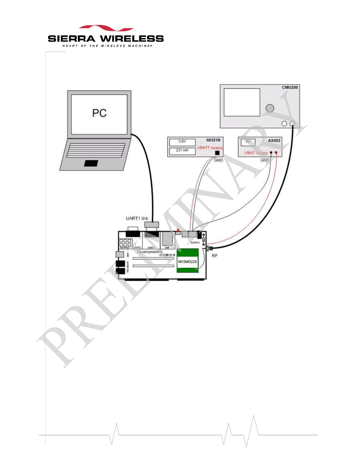
WA_DEV_W228_PTS_002 Rev 001 Page 90 of 108
Product Technical Specification &
Customer Design Guidelines
Figure 46. Typical Hardware Configuration
ThecommunicationtesterisaCMU200fromRhode&Schwartz.ThistesteroffersallGSM/GPRS
networkconfigurationsrequiredandallowsawiderangeofnetworkconfigurationstobeset.
TheAX502standalonepowersupplyisusedtosupplyallmotherboardcomponentsexceptthe
WISMO228.ThisisdonewiththeobjectivetoseparatetheWISMO218DevelopmentKitboard
consumptionfromtheWISMO228consumption–whichismeasuredbytheotherpowersupply,
the66321Bcurrentmeasuringpowersupply.Boththestandalonepowersupplyandthecurrent
measuringpowersupplyareconnectedtoandcontrolledbythecomputer(GPIBcontrol,whichis
notshowninthefigure).
Thestandalonepowersupply,AX502(orVBAT),maybesetfrom3.2Vto4.8V;whilethecurrent
measurepowersupply,66321B(orVBATT),mayalsobesetfrom3.2Vto4.8accordingtothe
WISMO228VBATTspecifications.
ASIMmustbeinsertedintheWISMO218DevelopmentKitduringallconsumptionmeasurement.
Thefollowingtableliststherecommendedequipmentstousefortheconsumptionmeasurement.
WA_DEV_W228_PTS_002 Rev 001 Page 91 of 108
Product Technical Specification &
Customer Design Guidelines
Table 42. List of Recommended Equipments
Device Manufacturer Reference Notes
Communication Tester Rhode & Schwartz CMU 200 Quad Band
GSM/DCS/GPRS
Current measuring
power supply Agilent 66321B
Used for VBATT (supplies the
WISMO228)
Stand alone power
supply Metrix AX502
Used for VBAT (supplies the
WISMO218 development kit board)
WISMO218 Development Kit
TheWISMO218DevelopmentKitisusedasabasisfortheWISMO228measurementviaanadaptor
boardandisusedtoperformconsumptionmeasurementusingseveralsettings.Refertothe
WISMO218DevelopmentKitUserGuideandtheWISMO218HardwarePresentationformore
informationaboutthesesettings.
Note: The WISMO218 Development Kit can be replaced by WMP100 Development Kit once a suitable
socket-up board is available.
TheWISMO218DevelopmentKitboardispoweredbythestandalonepowersupplyatVBAT;while
theWISMO228ispoweredbythecurrentmeasuringpowersupplyatVBATT.Itisforthisreason
thatthelinkbetweenVBATTandVBAT(J605)mustbeopened(byremovingthesolderatthetopof
theboardintheSUPPLYarea).Notethefollowinginformationregardingbothpowersupplies.
• VBATTispoweredbythecurrentmeasuringpowersupply(66321B)
• VBATispoweredbythestandalonepowersupply(AX502)throughTP602
Alsotakenoteofthefollowingadditionalconfiguration/settings:
• TheR600resistorandtheD603andD604diodes(aroundtheBAT‐TEMPconnector)must
beremoved.
• TheUART2linkisnotused;therefore,J201,J202,J203,J204mustbeopened(byremoving
thesolder).
• The“FLASH‐LED”mustbenotused,soJ602mustbeopened(byremovingthesolder).
• TheUSBlinkisnotused;therefore,J301,J302,J303,J304,J305mustbeopened(byremoving
thesolder).
• Audioisnotused;therefore,J702,J703,J704,J705,J605mustbeopened(byremovingthe
solder).
• ThereisnoSIMdetectfeatureontheWISMO228;therefore,J403mustbeopened(by
removingthesoldered).
• Chargingisnotused;therefore,R602mustberemoved.
• C600andR607mustberemovedtoavoidunexpectedcurrentconsumption.
• Theswitch,BOOT(aroundthe“CONFIG”area),mustbesettotheOFFposition.

WA_DEV_W228_PTS_002 Rev 001 Page 92 of 108
Product Technical Specification &
Customer Design Guidelines
ThegoalofthesettingslistedaboveistoeliminateallbiascurrentfromVBATTandtosupplythe
entireboard(excepttheWISMO228)usingonlyVBAT.
Socket-Up Board
Anadaptorboard,theWISMO218Socket‐UpBoard(WM0801706‐020‐20),isusedtoconnectthe
WISMO228toworkontheWISMO218DevelopmentKit.
Onthissocket‐upboard,thesolderingpointsofJ203,J204,JP101,JP102,JP103,JP104,JP105,JP106
andJP107mustbeopened.
SIM Cards
Consumptionmeasurementmaybeperformedwitheither3‐Voltor1.8‐VoltSIMcards.However,
allspecifiedconsumptionvaluesarefora3‐VoltSIMcard.
Caution: The SIM card’s voltage is supplied by the WISMO228’s power supply. Consumption measurement
results may vary depending on the SIM card used.
Software Configuration
Thissectiondiscussesthesoftwareconfigurationfortheequipment(s)usedandtheWISMO228
settings.
WISMO228 Configuration
TheWISMO228softwareconfigurationissimplyperformedbyselectingtheoperatingmodetouse
inperformingthemeasurement.
Adescriptionoftheoperatingmodesandtheproceduresusedtochangetheoperatingmodeare
givenintheappendixofWISMO218ATCommandsManual.
TheavailableoperatingmodesintheWISMO228areasfollows:
• OFFMode
• AlarmMode
• IdleMode
• ConnectedMode
• TransferModeclass8(4Rx/1Tx)(inGPRSmode)
• TransferModeclass10(3Rx/2Tx)(inGPRSmode)
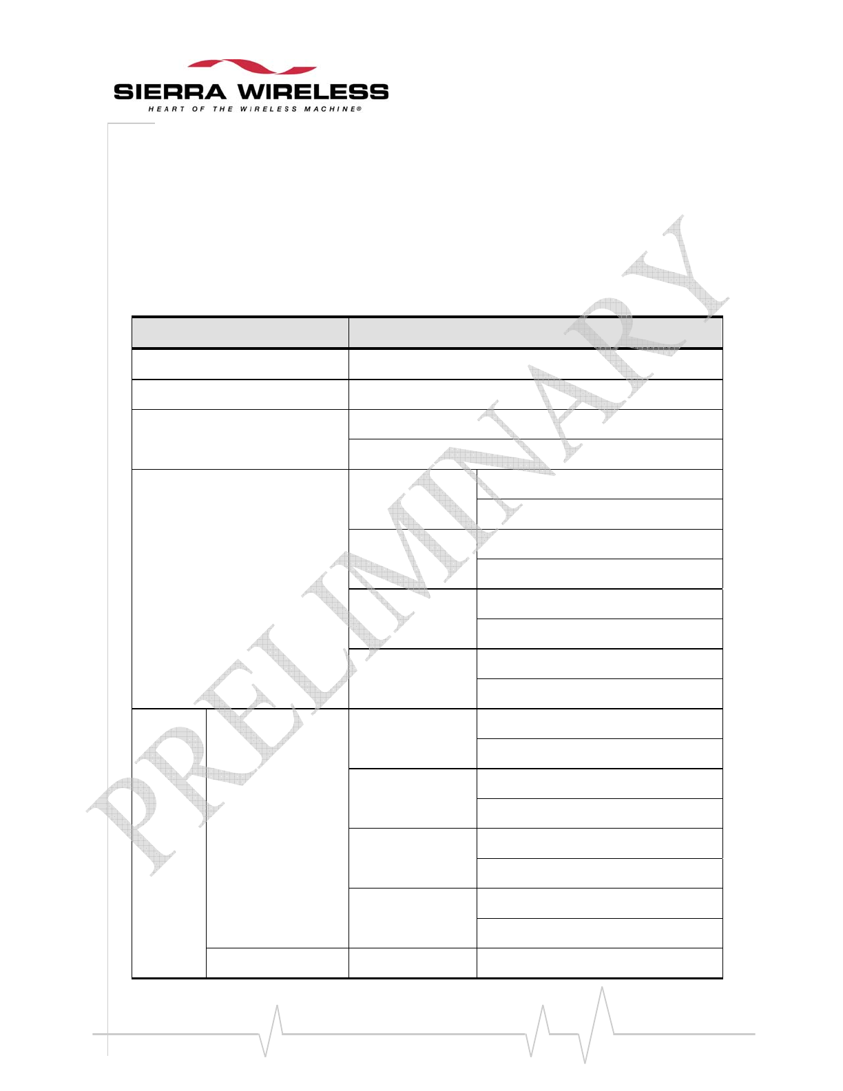
WA_DEV_W228_PTS_002 Rev 001 Page 93 of 108
Product Technical Specification &
Customer Design Guidelines
Equipment Configuration
ThecommunicationtesterissetaccordingtotheWISMO228operatingmode.Pagingduringidle
modes,TXburstpower,RFbandandGSM/DCS/GPRSmaybeselectedonthecommunication
tester.
Refertothefollowingtableforthenetworkanalyzerconfigurationaccordingtooperatingmode.
Table 43. Operating Mode Information
Operating Mode Communication Tester Configuration
OFF Mode N/A
Alarm Mode N/A
Idle Mode
Paging 2 (Rx burst occurrence ~0,5s)
Paging 9 (Rx burst occurrence ~2s)
Connected Mode
850 MHz
PCL5 (TX power 33dBm)
PCL19 (TX power 5dBm)
900 MHz
PCL5 (TX power 33dBm)
PCL19 (TX power 5dBm)
1800MHz
PCL0 (TX power 30dBm)
PCL15 (TX power 0dBm)
1900 MHz
PCL0 (TX power 30dBm)
PCL15 (TX power 0dBm)
GPRS
Transfer Mode class 8
(4Rx/1Tx)
850 MHz
Gam.3 (TX power 33dBm)
Gam.17 (TX power 5dBm)
900 MHz
Gam.3 (TX power 33dBm)
Gam.17 (TX power 5dBm)
1800MHz
Gam.3 (TX power 30dBm)
Gam.18 (TX power 0dBm)
1900 MHz
Gam.3 (TX power 30dBm)
Gam.18 (TX power 0dBm)
Transfer Mode class 10 850 MHz Gam.3 (TX power 33dBm)
WA_DEV_W228_PTS_002 Rev 001 Page 94 of 108
Product Technical Specification &
Customer Design Guidelines
Operating Mode Communication Tester Configuration
(3Rx/2Tx) Gam.17 (TX power 5dBm)
900 MHz
Gam.3 (TX power 33dBm)
Gam.17 (TX power 5dBm)
1800MHz
Gam.3 (TX power 30dBm)
Gam.18 (TX power 0dBm)
1900 MHz
Gam.3 (TX power 30dBm)
Gam.18 (TX power 0dBm)
Template
Thistemplatemaybeusedforconsumptionmeasurementforallmodesandconfigurations
available.NotethatthreeVBATTvoltagesareusedtomeasureconsumption,namely:VBATTmin
(3.2V),VBATTtyp(3.6V)andVBATTmax(4.8V).Theminimum/maximumRFtransmissionpower
configurationsarealsosetandmeasured.
Table 44. WISMO228 Power Consumption
WISMO228 Power Consumption
Operating Mode Parameters IMIN
average
VBATT=4.8V
INOM
average
VBATT=3.6V
IMAX
average
VBATT=3.2
V
IMAX peak Unit
Off Mode* µA
Alarm Mode µA
Idle Mode
TBD
mA
Paging 9 (Rx burst
occurrence ~2s) mA
Connected Mode
850 MHz
PCL5 (TX
power 33dBm) mA
PCL19 (TX
power 5dBm) mA
900 MHz PCL5 (TX
power 33dBm) mA
WA_DEV_W228_PTS_002 Rev 001 Page 95 of 108
Product Technical Specification &
Customer Design Guidelines
PCL19 (TX
power 5dBm) mA
1800 MHz
PCL0 (TX
power 30dBm) mA
PCL15 (TX
power 0dBm) mA
1900 MHz
PCL0 (TX
power 30dBm) mA
PCL15 (TX
power 0dBm)
mA
GPRS
Transfer
Mode class
8 (4Rx/1Tx)
850 MHz
Gam.3 (TX
power 33dBm) mA
Gam.17 (TX
power 5dBm)
mA
900 MHz
Gam.3 (TX
power 33dBm) mA
Gam.17 (TX
power 5dBm)
mA
1800 MHz
Gam.3 (TX
power 30dBm) mA
Gam.18 (TX
power 0dBm)
mA
1900 MHz
Gam.3 (TX
power 30dBm) mA
Gam.18 (TX
power 0dBm)
mA
Transfer
Mode class
10 (3Rx/2Tx)
850 MHz
Gam.3 (TX
power 33dBm) mA
Gam.17 (TX
power 5dBm)
mA
900 MHz
Gam.3 (TX
power 33dBm) mA
Gam.17 (TX
power 5dBm)
mA
1800 MHz
Gam.3 (TX
power 30dBm) mA
Gam.18 (TX
power 0dBm)
mA

WA_DEV_W228_PTS_002 Rev 001 Page 96 of 108
Product Technical Specification &
Customer Design Guidelines
1900 MHz
Gam.3 (TX
power 30dBm) mA
Gam.18 (TX
power 0dBm)
mA
* Current consumption in OFF mode is measured with BAT-RTC being left open.
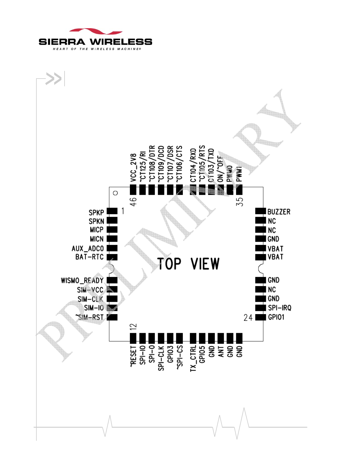
WA_DEV_W228_PTS_002 Rev 001 Page 97 of 108
Product Technical Specification &
Customer Design Guidelines
6. Technical Specifications
Castellation Pins
Pin Configuration
Figure 47. WISMO228 Pin Configuration
WA_DEV_W228_PTS_002 Rev 001 Page 98 of 108
Product Technical Specification &
Customer Design Guidelines
Pin Description
Table 45. WISMO228 Castellation Pin Description
Pin # Signal Description I/O Pin # Signal Description I/O
1 SPKP Speaker output
positive 32 ohms Analog 24 GPIO1 2.8V GPIO I/O
2 SPKN Speaker output
negative 32 ohms Analog 25 SPI-IRQ 2.8V SPI interrupt
request input I
3 MICP Microphone input
positive Analog 26 GND Ground Ground
4 MICN Microphone input
negative Analog 27 NC Not connected -
5 AUX_ADC
0 Analog to digital
converter I 28 GND Ground Ground
6 BAT-RTC Power supply for RTC
backup I 29 VBATT Power supply I
7 WISMO_R
EADY 2.8V WISMO Ready O 30 VBATT Power supply I
8 SIM-VCC SIM power supply O 31 GND Ground Ground
9 SIM-CLK SIM clock O 32 NC Not connected -
10 SIM-IO SIM data I/O 33 NC Not connected -
11 ~SIM-RST SIM reset O 34 BUZZER 2.8V Buzzer PWM2 O
12 ~RESET input reset signal I 35 PWM1 2.8V DC PWM 1 O
13 SPI-IO 2.8V SPI data input I/O 36 PWM0 2.8V DC PWM 0 O
14 SPI-O 2.8V SPI data output O 37 On/~OFF Power On control
signal I
15 SPI-CLK 2.8V SPI clock output O 38 CT103/T
XD* 2.8V UART1:
Transmit data I
16 GPIO3 2.8V GPIO I/O 39 ~CT105/
RTS* 2.8V UART1:
Request to send I
17 ~SPI-CS 2.8V SPI chip select
output O 40 CT104/R
XD* 2.8V UART1:
Receive data O
18 TX_CTRL 2.8V TX Burst
Indicator O 41 ~CT106/
CTS* 2.8V UART1: Clear
to send O
WA_DEV_W228_PTS_002 Rev 001 Page 99 of 108
Product Technical Specification &
Customer Design Guidelines
Pin # Signal Description I/O Pin # Signal Description I/O
19 GPIO5 2.8V GPIO I/O 42 ~CT107/
DSR 2.8V UART1: Data
set ready O
20 GND Ground Ground 43 ~CT109/
DCD 2.8V UART1: Data
carrier detect O
21 ANT Radio antenna
connection I/O 44 ~CT108/
DTR 2.8V UART1: Data
terminal ready I
22 GND Ground Ground 45 ~CT125/
RI 2.8V UART1: Ring
indicator O
23 GND Ground Ground 46 VCC_2V
8 2.8V power supply
from module O
* UART signal names are according to PC view.
* The I/O direction information only concerns the nominal signal. When the signal is configured in GPIO, it can
either be an Input or an Output.
Recommended Connection When Not Used
Thetablebelowgivestherecommendedconnectionforanyunusedpins.
Table 46. Recommended Connection When Not Used
Pin # Signal Recommended
Connection When Not
Used Pin # Signal Recommended
Connection When Not
Used
1
SPKP Open
24
GPIO1 Open
2
SPKN Open
25
SPI-IRQ PCB test point
3
MICP Open
26
GND Ground
4
MICN Open
27
NC Not connected
5
AUX_ADC0 Ground
28
GND Ground
6
BAT-RTC Open
29
VBATT Power supply
7
WISMO_READY Open
30
VBATT Power supply
8
SIM-VCC SIM power supply
31
GND Ground
9
SIM-CLK SIM clock
32
NC Not connected
10
SIM-IO SIM data
33
NC Not connected
11
~SIM-RST SIM reset
34
BUZZER Open
WA_DEV_W228_PTS_002 Rev 001 Page 100 of 108
Product Technical Specification &
Customer Design Guidelines
Pin # Signal Recommended
Connection When Not
Used Pin # Signal Recommended
Connection When Not
Used
12
~RESET Open
35
PWM1 Open
13
SPI-IO PCB test point
36
PWM0 Open
14
SPI-O PCB test point
37
On/~OFF Power On control signal
15
SPI-CLK PCB test point
38
CT103/TXD* 2.8V UART1: Transmit data
16
GPIO3 Open
39
~CT105/RTS* Connect to ~CT106/CTS
17
~SPI-CS PCB test point
40
CT104/RXD* 2.8V UART1: Receive data
18
TX_CTRL Not Connected
41
~CT106/CTS* Connect to ~CT105/RTS*
19
GPIO5 Open
42
~CT107/DSR Connect to ~CT108/DTR**
20
GND Ground
43
~CT109/DCD Open
21
ANT Radio antenna connection
44
~CT108/DTR Connect to ~CT107/DSR**
22
GND Ground
45
~CT125/RI Open
23
GND Ground
46
VCC_2V8 Open
* The I/O direction information only concerns the nominal signal. When the signal is configured in GPIO, it can
either be an Input or an Output.
** Refer to Table 11: Main Serial Link Pin
Description of the section discussing the SPI Bus
for Debug Trace ONLY
TheWISMO228providesoneSPIbusthroughthecastellationpin.
Caution: This interface is only used for monitoring trace for debug purposes.
Pin Description
ThefollowingtableprovidesthepindescriptionoftheSPIbus.
Table 47. SPI Bus Pin Description
Pin # Signal I/O I/O Type Reset State Description
13 SPI-IO I/O 2V8 Pull down SPI Serial input/output
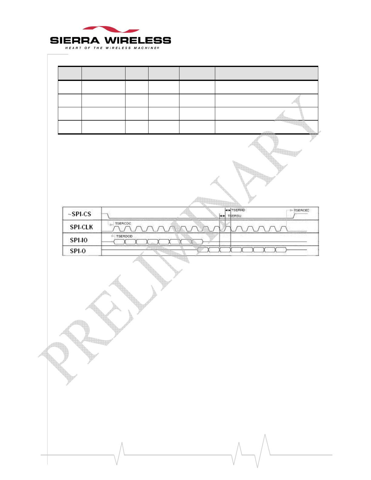
WA_DEV_W228_PTS_002 Rev 001 Page 101 of 108
Product Technical Specification &
Customer Design Guidelines
Pin # Signal I/O I/O Type Reset State Description
14 SPI-O O 2V8 Pull down SPI Serial input
15 SPI-CLK O 2V8 Pull down SPI Serial Clock
17 ~SPI-CS O 2V8 Pull up SPI Enable
25 SPI-IRQ I 2V8 Pull down SPI Interrupt
AnSPI‐to‐UART2conversioncircuitisrequiredtoconverttheSPItracetoUART2.Also,theSPI‐
IRQ(pin25)isrequiredforinterrupt.Again,notethattheSPIinterfaceoftheWISMO228isnot
openforapplicationuseotherthandebugtrace.
SPI Waveforms
Figure 48. SPI Timing Diagram

WA_DEV_W228_PTS_002 Rev 001 Page 102 of 108
Product Technical Specification &
Customer Design Guidelines
Figure 49. Example of an SPI to UART2 Interface Conversion Implementation
ThefollowingtableliststherecommendedcomponentstouseinimplementingtheSPItoUART2
interface.
Component Description/Details Manufacturer
U103 SC16IS750IPW NXP Semiconductors
X101 3, 6864MHz 86SMX surface mount crystal (971-
3131) Farnell
R104, R105 10KΩ
R106 1KΩ
C105 22pF
C106 33pF
C107 100nF
AfterconvertingtheSPIsignaltoaUARTsignal,aUARTtransceivercircuitryisneededto
communicatethisUARTsignaltotheDTE.
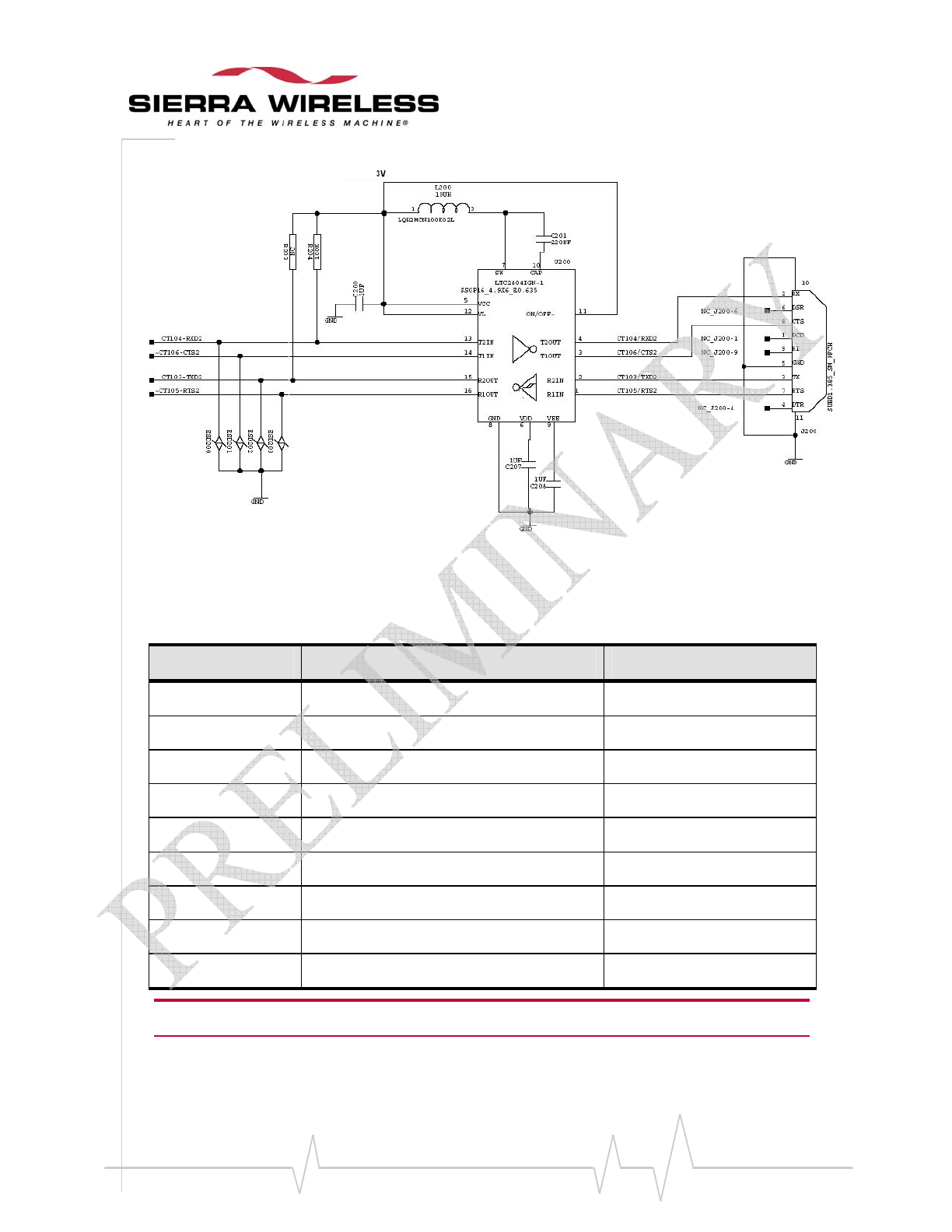
WA_DEV_W228_PTS_002 Rev 001 Page 103 of 108
Product Technical Specification &
Customer Design Guidelines
Figure 50. Example of an RS-232 Level Shifter Implementation for UART2
ThefollowingtableliststherecommendedcomponentstouseinimplementingaUARTtransceiver
circuitry.
Component Description/Details Manufacturer
U200 LTC2804IGN-1 LINEAR TECHNOLOGY
L200 LQH2M CN100K02L MURATA
J200 096615276119 SUBD9F HARTING
R202 NC
R204 100KΩ
C200 1µF
C201 220nF
C207 1µF
C208 1µF
Note: It is recommended to make SPI signals accessible for diagnostics by reserving some test points, for
example.
Main Serial Link (UART) for more information regarding the connection between DSR and DTR.
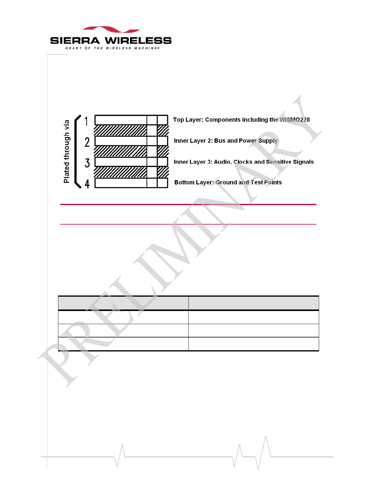
WA_DEV_W228_PTS_002 Rev 001 Page 104 of 108
Product Technical Specification &
Customer Design Guidelines
PCB Specifications for the Application Board
Inordertosavecostsforsimpleapplications,acheapPCBstructurecanbeusedfortheapplication
boardoftheWISMO228.A4‐layerthrough‐holetypePCBstructurecanbeused.
Figure 51. PCB Structure Example for the Application Board
Note: Due to the limited layers of 4-layer PCBs, sensitive signals like audio, SIM and clocks cannot be
protected by 2 adjacent ground layers. As a result, care must be taken during PCB layout for these
sensitive signals by avoiding coupling to noisy baseband through adjacent layers.
Environmental Specifications
TheWISMO228iscompliantwiththefollowingoperatingclasses.Thetablebelowliststheideal
temperaturerangeoftheenvironment.
Table 48. Operating Class Temperature Range
Conditions Temperature Range
Operating / Class A -20 °C to +55°C
Operating / Class B -40 °C to +85°C
Storage -40 °C to +85°C
Function Status Classification
Class A
TheWISMO228remainsfullyfunctional,meetingGSMperformancecriteriainaccordancewith
ETSIrequirements,acrossthespecifiedtemperaturerange.
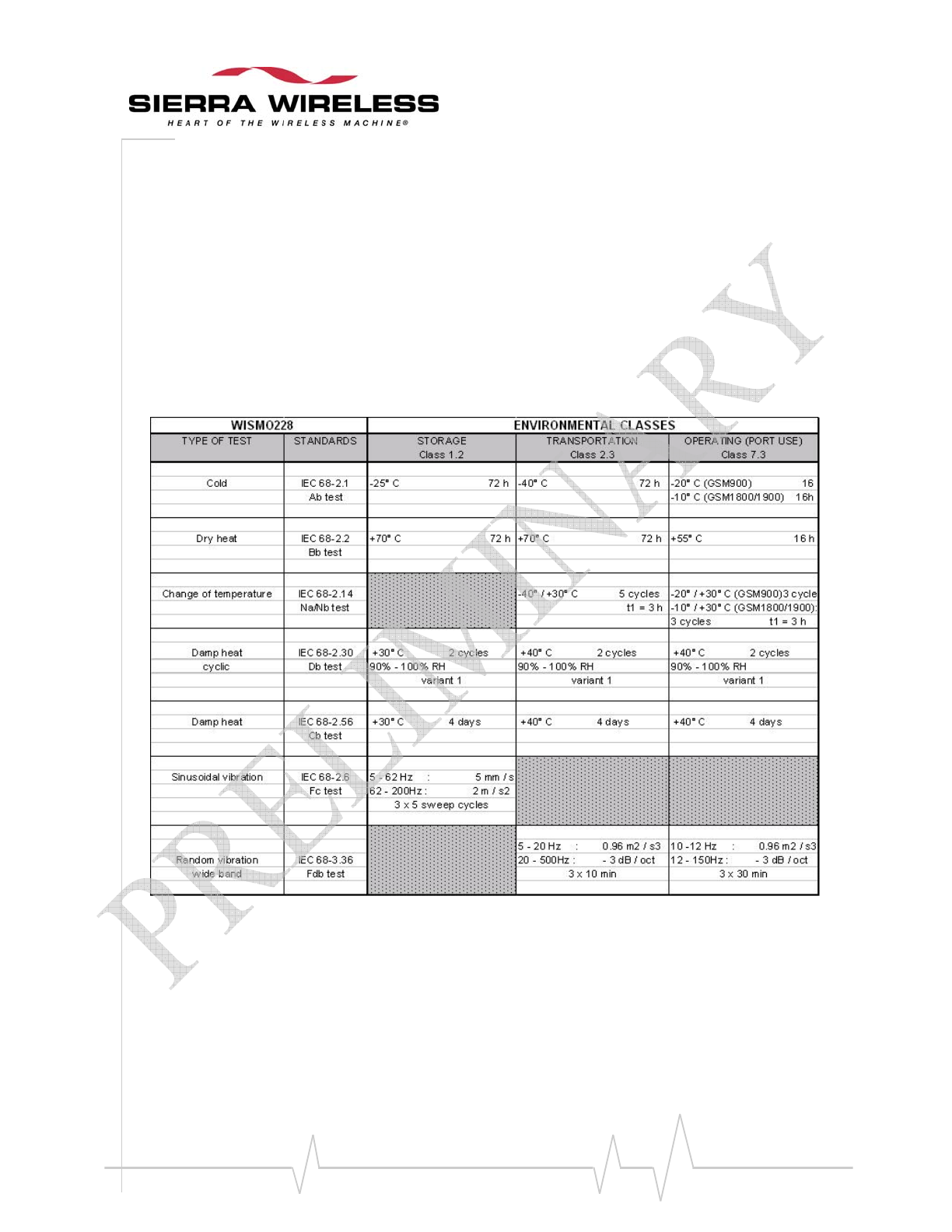
WA_DEV_W228_PTS_002 Rev 001 Page 105 of 108
Product Technical Specification &
Customer Design Guidelines
Class B
TheWISMO228remainsfullyfunctionalacrossthespecifiedtemperaturerange.SomeGSM
parametersmayoccasionallydeviatefromtheETSIspecifiedrequirementsandthisdeviationdoes
notaffecttheabilityoftheWISMO228toconnecttothecellularnetworkandbefullyfunctional,as
itdoeswithintheClassArange.
Thedetailedclimaticandmechanicsstandardenvironmentalconstraintsapplicabletothe
WISMO228arelistedinthetablebelow.
Table 49. Environmental Classes

WA_DEV_W228_PTS_002 Rev 001 Page 106 of 108
Product Technical Specification &
Customer Design Guidelines
Mechanical Specifications
Physical Characteristics
TheWISMO228hasanearly‐completeself‐containedshield.
• Overalldimensions:25.0x25.0x2.8mm(excludinglabelthickness)
• Weight:3.64g
Recommended PCB Landing Pattern
RefertotheCustomerProcessGuidelineforWISMOSeriesdocument.
WISMO228 Dimensions
<tofollow>
Figure 52. WISMO228 Dimensions

WA_DEV_W228_PTS_002 Rev 001 Page 107 of 108
Product Technical Specification &
Customer Design Guidelines
7. Recommended Peripheral
Devices
General Purpose Connector
Thegeneralpurposeconnectorisa46‐pincastellationconnectorwitha1.5mmpitch.
SIM Card Reader
ListedbelowaretherecommendedSIMCardReaderstousewiththeWISMO228.
• ITTCANNONCCM03series(seehttp://www.ittcannon.com)
• AMPHENOLC707series(seehttp://www.amphenol.com)
• JAE(seehttp://www.jae.co.jp/e‐top/index.html)
Drawertype:
• MOLEX99228‐0002(connector)/MOLEX91236‐0002(holder)(seehttp://www.molex.com)
Microphone
Microphonescanbeobtainedfromthefollowingrecommendedsuppliers:
• HOSIDEN
• PANASONIC
• PEIKER
Speaker
Speakerscanbeobtainedfromthefollowingrecommendedsuppliers:
• SANYO
• HOSIDEN
• PRIMO
• PHILIPS

WA_DEV_W228_PTS_002 Rev 001 Page 108 of 108
Product Technical Specification &
Customer Design Guidelines
Antenna Cable
ListedbelowaretherecommendedantennacablestomountontheWISMO228.
• RG178
• RG316
GSM Antenna
GSMantennasandsupportforantennaadaptationcanbeobtainedfrommanufacturerssuchas:
• ALLGON(http://www.allgon.com)
• HIRSCHMANN(http://www.hirschmann.com/)

WA_DEV_W228_PTS_002 Rev 001 Page 109 of 109
Product Technical Specification &
Customer Design Guidelines
8. Noises and Design
EMC Recommendations
EMCtestshavetobeperformedassoonaspossibleontheapplicationtodetectanypossible
problems.
WhendesigningaGSMterminal,makesuretotakenoteofthefollowingitems:
• PossiblespuriousemissionsradiatedbytheapplicationtotheRFreceiverinthereceiver
band.
• ESDprotectionismandatoryforallperipheralsaccessiblefromoutside(SIM,seriallink,
audio,AUX_ADC0,etc.).
• EMCprotectiononaudioinput/output(filtersagainst900MHzemissions).
• Biasingofthemicrophoneinputs.
• LengthoftheSIMinterfacelines(preferably<10cm).
• Groundplane:Itisrecommendedtohaveacommongroundplaneforanalog/digital/RF
grounds.
• Itisrecommendedtouseametalliccaseorplasticcasingwithconductivepaint.
Power Supply
ThepowersupplyisoneofthekeyissuesinthedesignofaGSMterminalandcarefulattention
shouldbepaidtothefollowing:
• Qualityofthepowersupply:lowripple,PFMorPSMsystemsshouldbeavoided(usinga
PWMconverterispreferred).
• Thecapacitytodeliverhighcurrentpeaksinashorttime(pulsedradioemission).
Aweakpowersupplydesigncouldaffectthefollowingitemsspecifically:
• EMCperformances
• Theemissionsspectrum
• Phaseerrorandfrequencyerror
Overvoltage
TheWISMO228doesnotincludeanyprotectionagainstovervoltage.
WA_DEV_W228_PTS_002 Rev 001 Page 110 of 110
Product Technical Specification &
Customer Design Guidelines
9. Appendix
Standards and Recommendations
GSM ETSI, 3GPP, and GCF recommendations for Phase II
Specification Reference Title
3GPP TS 45.005 v5.5.0 (2002-08)
Release 5 Technical Specification Group GSM/EDGE. Radio Access Network;
Radio transmission and reception
GSM 02.07 V8.0.0 (1999-07) Digital cellular telecommunications system (Phase 2+);
Mobile Stations (MS) features (GSM 02.07 version 8.0.0 Release 1999)
GSM 02.60 V8.1.0 (1999-07)
Digital cellular telecommunications system (Phase 2+);
General Packet Radio Service (GPRS); Service description, Stage 1
(GSM 02.60 version 8.1.0 Release 1999)
GSM 03.60 V7.9.0 (2002-09)
Technical Specification Group Services and System Aspects;
Digital cellular telecommunications system (Phase 2+); General Packet
Radio Service (GPRS); Service description; Stage 2 (Release 1998)
3GPP TS 43.064 V5.0.0 (2002-04)
Technical Specification Group GERAN; Digital cellular
telecommunications system (Phase 2+); General Packet Radio Service
(GPRS); Overall description of the GPRS radio interface; Stage 2
(Release 5)
3GPP TS 03.22 V8.7.0 (2002-08) Technical Specification Group GSM/EDGE. Radio Access Network;
Functions related to Mobile Station (MS) in idle mode and group receive
mode; (Release 1999)
3GPP TS 03.40 V7.5.0 (2001-12)
Technical Specification Group Terminals;
Technical realization of the Short Message Service (SMS)
(Release 1998)
3GPP TS 03.41 V7.4.0 (2000-09) Technical Specification Group Terminals; Technical realization of Cell
Broadcast Service (CBS) (Release 1998)
ETSI EN 300 903 V8.1.1 (2000-11)
Digital cellular telecommunications system (Phase 2+);
Transmission planning aspects of the speech service in the GSM
Public Land Mobile Network (PLMN) system (GSM 03.50 version 8.1.1
Release 1999)
3GPP TS 04.06 V8.2.1 (2002-05) Technical Specification Group GSM/EDGE Radio Access Network;
Mobile Station - Base Station System (MS - BSS) interface; Data Link
(DL) layer specification (Release 1999)
WA_DEV_W228_PTS_002 Rev 001 Page 111 of 111
Product Technical Specification &
Customer Design Guidelines
Specification Reference Title
3GPP TS 04.08 V7.18.0 (2002-09)
Technical Specification Group Core Network;
Digital cellular telecommunications system (Phase 2+);
Mobile radio interface layer 3 specification (Release 1998)
3GPP TS 04.10 V7.1.0 (2001-12)
Technical Specification Group Core Networks;
Mobile radio interface layer 3 Supplementary services specification;
General aspects (Release 1998)
3GPP TS 04.11 V7.1.0 (2000-09)
Technical Specification Group Core Network; Digital cellular
telecommunications system (Phase 2+); Point-to-Point (PP) Short
Message Service (SMS) support on mobile radio interface
(Release 1998)
3GPP TS 45.005 v5.5.0 (2002-08) Technical Specification Group GSM/EDGE. Radio Access Network;
Radio transmission and reception (Release 5)
3GPP TS 45.008 V5.8.0 (2002-08) Technical Specification Group GSM/EDGE
Radio Access Network; Radio subsystem link control (Release 5)
3GPP TS 45.010 V5.1.0 (2002-08) Technical Specification Group GSM/EDGE
Radio Access Network; Radio subsystem synchronization (Release 5)
3GPP TS 46.010 V5.0.0 (2002-06) Technical Specification Group Services and System Aspects;
Full rate speech; Transcoding (Release 5)
3GPP TS 46.011 V5.0.0 (2002-06)
Technical Specification Group Services and System Aspects;
Full rate speech; Substitution and muting of lost frames for
full rate speech channels (Release 5)
3GPP TS 46.012 V5.0.0 (2002-06)
Technical Specification Group Services and System Aspects;
Full rate speech; Comfort noise aspect for full rate speech traffic
channels (Release 5)
3GPP TS 46.031 V5.0.0 (2002-06)
Technical Specification Group Services and System Aspects;
Full rate speech; Discontinuous Transmission (DTX) for full rate speech
traffic channels (Release 5)
3GPP TS 46.032 V5.0.0 (2002-06)
Technical Specification Group Services and System Aspects;
Full rate speech; Voice Activity Detector (VAD) for full rate speech traffic
channels (Release 5)
TS 100 913V8.0.0 (1999-08)
Digital cellular telecommunications system (Phase 2+);
General on Terminal Adaptation Functions (TAF) for Mobile Stations
(MS) (GSM 07.01 version 8.0.0 Release 1999)
WA_DEV_W228_PTS_002 Rev 001 Page 112 of 112
Product Technical Specification &
Customer Design Guidelines
Specification Reference Title
GSM 09.07 V8.0.0 (1999-08)
Digital cellular telecommunications system (Phase 2+);
General requirements on interworking between the Public Land Mobile
Network (PLMN) and the Integrated Services Digital Network (ISDN) or
Public Switched Telephone Network (PSTN) (GSM 09.07 version 8.0.0
Release 1999)
3GPP TS 51.010-1 v5.0.0 (2002-
09)
Technical Specification Group GSM/EDGE ; Radio Access
Network ;Digital cellular telecommunications system (Phase 2+);Mobile
Station (MS) conformance specification; Part 1: Conformance
specification (Release 5)
3GPP TS 51.011 V5.0.0 (2001-12) Technical Specification Group Terminals; Specification of the Subscriber
Identity Module - Mobile Equipment (SIM - ME) interface (Release 5)
ETS 300 641 (1998-03)
Digital cellular telecommunications system (Phase 2);
Specification of the 3 Volt Subscriber Identity Module - Mobile Equipment
(SIM-ME) interface (GSM 11.12 version 4.3.1)
GCF-CC V3.7.1 (2002-08) Global Certification Forum – Certification criteria
TheWISMO228canonlybeusedformobileandfixedapplications.Theantenna(s)usedforthe
transmittermustbeinstalledataminimumdistanceof20cmfromallpersonsandmustnotbeco‐
locatedoroperatedwithanyotherantennaortransmitter.
Usersandinstallersmustbeprovidedwithantennainstallationinstructionsandtransmitter
operatingconditionsforsatisfyingRFexposurecompliance.
Notethatwheninstalledinportabledevices,theRFexposureconditionrequiresaseparate
mandatoryequipmentauthorizationforthefinaldevice.

WA_DEV_W228_PTS_002 Rev 001 Page 113 of 113
Product Technical Specification &
Customer Design Guidelines
Safety Recommendations (for Information Only)
Warning: For the efficient and safe operation of your GSM application
based on the WISMO228, please read the following information
carefully.
RF Safety
General
YourGSMterminalisbasedontheGSMstandardforcellulartechnology.TheGSMstandardis
spreadallovertheworld.ItcoversEurope,AsiaandsomepartsofAmericaandAfrica.Thisisthe
mostusedtelecommunicationstandard.
YourGSMterminalisactuallyalowpowerradiotransmitterandreceiver.Itsendsoutandreceives
radiofrequencyenergy.WhenyouuseyourGSMapplication,thecellularsystemwhichhandles
yourcallscontrolsboththeradiofrequencyandthepowerlevelofyourcellularmodem.
ExposuretoRFEnergy
TherehasbeensomepublicconcernaboutpossiblehealtheffectsfromusingGSMterminals.
AlthoughresearchonhealtheffectsfromRFenergyhasfocusedonthecurrentRFtechnologyfor
manyyears,scientistshavebegunresearchregardingnewerradiotechnologies,suchasGSM.After
existingresearchhadbeenreviewed,andaftercompliancetoallapplicablesafetystandardshad
beentested,ithasbeenconcludedthattheproductwasfitforuse.
IfyouareconcernedaboutexposuretoRFenergytherearethingsyoucandotominimizeexposure.
Obviously,limitingthedurationofyourcallswillreduceyourexposuretoRFenergy.Inaddition,
youcanreduceRFexposurebyoperatingyourcellularterminalefficientlybyfollowingthe
guidelinesbelow.
EfficientTerminalOperation
ForyourGSMterminaltooperateatthelowestpowerlevel,consistentwithsatisfactorycallquality:
Ifyourterminalhasanextendibleantenna,extenditfully.Somemodelsallowyoutoplaceacall
withtheantennaretracted.However,yourGSMterminaloperatesmoreefficientlywiththeantenna
fullyextended.
Donotholdtheantennawhentheterminalis«INUSE».Holdingtheantennaaffectscallquality
andmaycausethemodemtooperateatahigherpowerlevelthanneeded.
AntennaCareandReplacement

WA_DEV_W228_PTS_002 Rev 001 Page 114 of 114
Product Technical Specification &
Customer Design Guidelines
DonotusetheGSMterminalwithadamagedantenna.Ifadamagedantennacomesintocontact
withtheskin,aminorburnmayresult.Replaceadamagedantennaimmediately.Consultyour
manualtoseeifyoumaychangetheantennayourself.Ifso,useonlyamanufacturer‐approved
antenna.Otherwise,haveyourantennarepairedbyaqualifiedtechnician.
Useonlythesuppliedorapprovedantenna.Unauthorizedantennas,modificationsorattachments
coulddamagetheterminalandmaycontravenelocalRFemissionregulationsorinvalidatetype
approval.
General Safety
Driving
Checkthelawsandtheregulationsregardingtheuseofcellulardevicesintheareawhereyouhave
todriveasyoualwayshavetocomplywiththem.WhenusingyourGSMterminalwhiledriving,
please:
• givefullattentiontodriving,
• pullofftheroadandparkbeforemakingoransweringacallifdrivingconditionsso
require.
ElectronicDevices
Mostelectronicequipment,forexampleinhospitalsandmotorvehicles,isshieldedfromRFenergy.
However,RFenergymayaffectsomeimproperlyshieldedelectronicequipment.
VehicleElectronicEquipment
Checkyourvehiclemanufacturerrepresentativetodetermineifanyon‐boardelectronicequipment
isadequatelyshieldedfromRFenergy.
MedicalElectronicEquipment
Consultthemanufacturerofanypersonalmedicaldevices(suchaspacemakers,hearingaids,etc...)
todetermineiftheyareadequatelyshieldedfromexternalRFenergy.
TurnyourterminalOFFinhealthcarefacilitieswhenanyregulationspostedintheareainstructyou
todoso.HospitalsorhealthcarefacilitiesmaybeusingRFmonitoringequipment.
Aircraft
TurnyourterminalOFFbeforeboardinganyaircraft.
• Useitonthegroundonlywithcrewpermission.
• Donotuseitintheair.

WA_DEV_W228_PTS_002 Rev 001 Page 115 of 115
Product Technical Specification &
Customer Design Guidelines
Topreventpossibleinterferencewithaircraftsystems,FederalAviationAdministration(FAA)
regulationsrequireyoutohavepermissionfromacrewmembertouseyourterminalwhilethe
aircraftisontheground.Topreventinterferencewithcellularsystems,localRFregulationsprohibit
usingyourmodemwhileairborne.
Children
DonotallowchildrentoplaywithyourGSMterminal.Itisnotatoy.Childrencouldhurt
themselvesorothers(bypokingthemselvesorothersintheeyewiththeantenna,forexample).
Childrencoulddamagethemodem,ormakecallsthatincreaseyourmodembills.
BlastingAreas
Toavoidinterferingwithblastingoperations,turnyourunitOFFwhenina«blastingarea»orin
areasposted:«turnofftwo‐wayradio».ConstructioncrewsoftenuseremotecontrolRFdevicesto
setoffexplosives.
PotentiallyExplosiveAtmospheres
TurnyourterminalOFFwheninanyareawithapotentiallyexplosiveatmosphere.Itisrare,but
yourapplicationoritsaccessoriescouldgeneratesparks.Sparksinsuchareascouldcausean
explosionorfireresultinginbodilyinjuriesorevendeath.
Areaswithapotentiallyexplosiveatmosphereareoften,butnotalways,clearlymarked.They
includefuellingareassuchaspetrolstations;belowdecksonboats;fuelorchemicaltransferor
storagefacilities;andareaswheretheaircontainschemicalsorparticles,suchasgrain,dust,or
metalpowders.
Donottransportorstoreflammablegas,liquid,orexplosivesinthecompartmentofyourvehicle
whichcontainsyourterminaloraccessories.
Beforeusingyourterminalinavehiclepoweredbyliquefiedpetroleumgas(suchaspropaneor
butane)ensurethatthevehiclecomplieswiththerelevantfireandsafetyregulationsofthecountry
inwhichthevehicleistobeused.