Sigma Designs ZM5304-U Z-Wave Serial Interface Module with On-Board Antenna User Manual
Sigma Designs Inc Z-Wave Serial Interface Module with On-Board Antenna
User Manual.pdf
DATASHEET: ZM5304
DSH12461-3 | 7/2013 1
FULLY INTEGRATED Z-WAVE® WIRELESS MODEM WITH
ON-BOARD ANTENNA
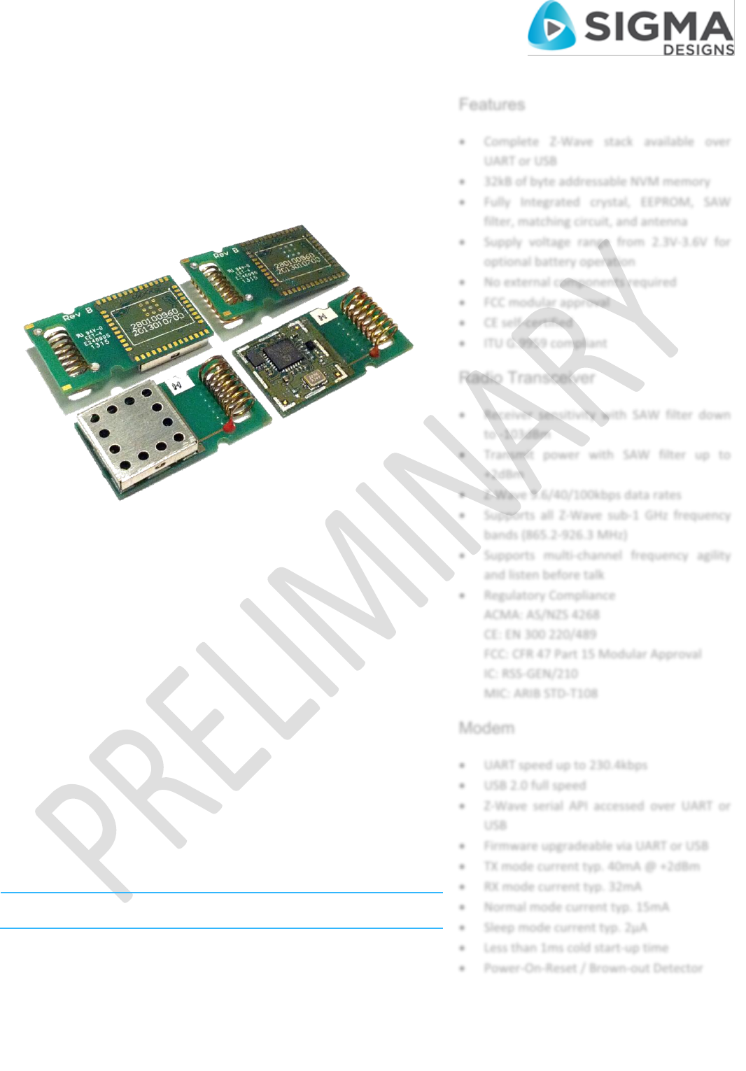
The Sigma Designs ZM5304 Modem is a fully integrated Z-Wave modem
module in a small 27mmx15.2mmx5.5mm form factor. It is an ideal
solution for home control applications such as access control, appliance
control, AV control, building automation, energy management, lighting,
security, and sensor networks in the “Internet of Things”.
A baseband controller, sub-1 GHz radio transceiver, crystal, decoupling,
SAW filter, matching, and the antenna is included to provide a complete
Z-Wave solution to an application executing in an external host
microcontroller. The ZM5304 Modem is certified with the FCC modular
approval, ready to be used in any product without additional testing and
license costs.
The ZM5304 Modem is based on an 8-bit 8051 CPU core, which is
optimized to handle the data and link management requirements of a
Z-Wave node. The UART or USB interface can be used to access the
Z-Wave stack available in the on-chip Flash memory, or to easily upgrade
the modem firmware.
FCC ID
TBD
IC ID
TBD
Features
Complete Z-Wave stack available over
UART or USB
32kB of byte addressable NVM memory
Fully Integrated crystal, EEPROM, SAW
filter, matching circuit, and antenna
Supply voltage range from 2.3V-3.6V for
optional battery operation
No external components required
FCC modular approval
CE self-certified
ITU G.9959 compliant
Radio Transceiver
Receiver sensitivity with SAW filter down
to -103dBm
Transmit power with SAW filter up to
+2dBm
Z-Wave 9.6/40/100kbps data rates
Supports all Z-Wave sub-1 GHz frequency
bands (865.2-926.3 MHz)
Supports multi-channel frequency agility
and listen before talk
Regulatory Compliance
ACMA: AS/NZS 4268
CE: EN 300 220/489
FCC: CFR 47 Part 15 Modular Approval
IC: RSS-GEN/210
MIC: ARIB STD-T108
Modem
UART speed up to 230.4kbps
USB 2.0 full speed
Z-Wave serial API accessed over UART or
USB
Firmware upgradeable via UART or USB
TX mode current typ. 40mA @ +2dBm
RX mode current typ. 32mA
Normal mode current typ. 15mA
Sleep mode current typ. 2µA
Less than 1ms cold start-up time
Power-On-Reset / Brown-out Detector

Datasheet: ZM5304
2 DSH12461-3 | 7/2013
1 CONTENT
2 OVERVIEW .......................................................................................................................................................................... 4
2.1 PERIPHERALS ........................................................................................................................................................................... 4
2.1.1 Advanced Encryption Standard Security Processor ..................................................................................................... 4
2.1.2 Analog-to-Digital Converter ........................................................................................................................................ 5
2.1.3 Crystal Driver and System Clock .................................................................................................................................. 5
2.1.4 Interrupt Controller ..................................................................................................................................................... 5
2.1.5 Power-On-Reset / Brown-Out Detector ....................................................................................................................... 6
2.1.6 Reset Controller ........................................................................................................................................................... 6
2.1.7 Universal Asynchronous Receiver / Transmitter ......................................................................................................... 6
2.1.8 Universal Serial Bus ..................................................................................................................................................... 6
2.1.9 Watchdog .................................................................................................................................................................... 7
2.1.10 Wireless Transceiver.................................................................................................................................................... 7
2.2 MEMORY MAP ........................................................................................................................................................................ 7
2.3 MODULE PROGRAMMING .......................................................................................................................................................... 8
2.3.1 Entering In-System Programming Mode ..................................................................................................................... 8
2.3.2 Entering Auto Programming Mode ............................................................................................................................. 8
2.4 POWER SUPPLY REGULATOR ...................................................................................................................................................... 8
3 TYPICAL APPLICATION ........................................................................................................................................................ 9
4 PAD CONFIGURATION ....................................................................................................................................................... 10
4.1 PAD FUNCTIONALITY ............................................................................................................................................................... 10
5 ELECTRICAL CHARACTERISTICS .......................................................................................................................................... 12
5.1 TEST CONDITIONS .................................................................................................................................................................. 12
5.1.1 Typical Values ............................................................................................................................................................ 12
5.1.2 Minimum and Maximum Values ............................................................................................................................... 12
5.2 ABSOLUTE MAXIMUM RATINGS ................................................................................................................................................ 13
5.3 GENERAL OPERATING RATINGS ................................................................................................................................................. 13
5.4 CURRENT CONSUMPTION ........................................................................................................................................................ 13
5.5 SYSTEM TIMING ..................................................................................................................................................................... 14
5.6 NON-VOLATILE MEMORY RELIABILITY ........................................................................................................................................ 15
5.7 ANALOG-TO-DIGITAL CONVERTER ............................................................................................................................................. 16
5.8 DC CHARACTERISTICS ............................................................................................................................................................. 16
5.9 RF CHARACTERISTICS .............................................................................................................................................................. 17
5.9.1 Transmitter................................................................................................................................................................ 17
5.9.2 Receiver ..................................................................................................................................................................... 18
5.9.3 Antenna ..................................................................................................................................................................... 21
5.9.4 Regulatory Compliance ............................................................................................................................................. 22
6 Z-WAVE FREQUENCIES ...................................................................................................................................................... 23
7 MODULE INFORMATION ................................................................................................................................................... 24
7.1 MODULE MARKING ................................................................................................................................................................ 24
7.2 MODULE DIMENSIONS ............................................................................................................................................................ 24
8 PCB MOUNTING AND SOLDERING..................................................................................................................................... 25
8.1 RECOMMENDED PCB MOUNTING PATTERN ................................................................................................................................ 25
8.2 RECOMMENDED PLACEMENT ON PCB ....................................................................................................................................... 26

Datasheet: ZM5304
DSH12461-3 | 7/2013 3
8.3 SOLDERING INFORMATION ....................................................................................................................................................... 26
9 ORDERING INFORMATION ................................................................................................................................................ 28
9.1 TAPE AND REEL INFORMATION ................................................................................................................................................. 29
10 REVISION HISTORY ........................................................................................................................................................ 31
11 REFERENCES .................................................................................................................................................................. 32
Datasheet: ZM5304
4 DSH12461-3 | 7/2013
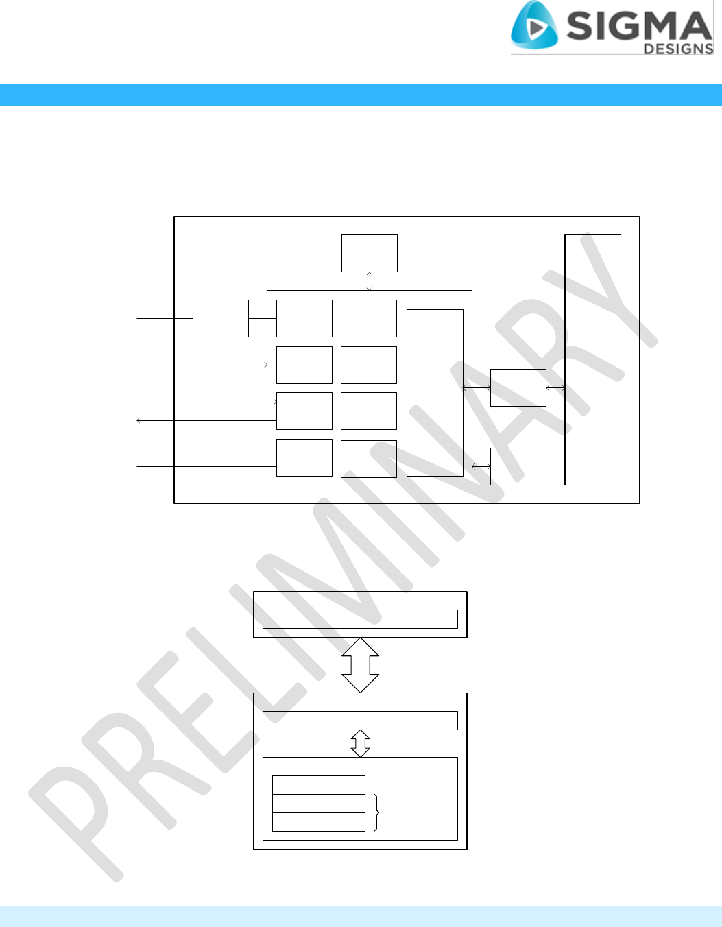
2 OVERVIEW
The ZM5304 Modem is a fully integrated module with an on-board antenna that allows the establishment of a Z-Wave network
with minimum risk. The SD3503 modem chip is used with an external NVM (EEPROM), 32MHz crystal, power supply decoupling,
SAW filter, matching circuit, and a helical antenna. Figure 2.1 shows the main blocks of the ZM5304 Modem, while Figure 2.2
illustrates the firmware stack of an example application.
EEPROM
Memory
ZM5304
TXD
USB_DP
RESET_N
USB_DM
RXD
VDD
SPI
Voltage
Regulator
UART
USB
Sub-1 GHz
Radio
Transceiver
SD3503
SAW Filter &
Matching
Helical
Antenna
32MHz
XTAL
8051 CPU
Decoupling
Flash
Memory
AES
ADC
POR / BOD
Figure 2.1: Functional block diagram
HOST
Application
UART / USB
ZM5304
Z-Wave® Serial API
Z-Wave® Protocol Stack
Network Layer
MAC Layer
PHY Layer ITU G.9959
Figure 2.2: Firmware stack
2.1 PERIPHERALS
2.1.1 ADVANCED ENCRYPTION STANDARD SECURITY PROCESSOR
The Z-Wave protocol specifies the use of Advanced Encryption Standard (AES) 128-bit block encryption for secure applications.
The built-in Security Processor is a hardware accelerator that encrypts and decrypts data at a rate of 1 byte per 1.5µs. It encodes

Datasheet: ZM5304
DSH12461-3 | 7/2013 5
the frame payload and the message authentication code to ensure privacy and authenticity of messages. The processor supports
Output FeedBack (OFB), Cipher-Block Chaining (CBC), and Electronic CodeBook (ECB) modes to target variable length messages.
Payload data is streamed in OFB mode, and authentication data is processed in CBC mode as required by the Z-Wave protocol.
The processor implements two efficient access methods: Direct Memory Access (DMA) and streaming through Special Function
Register (SFR) ports. The processor functionality is exposed via the Z-Wave API for application use.
2.1.2 ANALOG-TO-DIGITAL CONVERTER
The Analog-to-Digital Converter (ADC) is capable of sampling an input voltage source and returns an 8 or 12 bit unsigned
representation of the input scaled relative to the selected reference voltage, as described by the formula below.
The ADC is capable of operating rail to rail, while the following input configurations apply (VBG = built-in Band-gap 1.25V,
VDD = supply voltage):
Table 2.1: ADC voltage source configuration options
Source
Description
Pin
VIN
The sampling input voltage
VBG
VREF+
The positive node of the reference voltage
VBG, VDD
VREF-
The negative node of the reference voltage
GND
If the sampling input voltage crosses a predefined lower or upper voltage threshold, an interrupt is triggered. Setting VIN = VBG
and VRFE+ = VDD implements a battery monitor.
2.1.3 CRYSTAL DRIVER AND SYSTEM CLOCK
The system clock and RF frequencies are derived from an external 32MHz crystal (XTAL) which is factory trimmed to guarantee
initial frequency precision. The temperature and 5 years aging margin for the 32MHz crystal is 15 ppm.
2.1.4 INTERRUPT CONTROLLER
The interrupts are shared between the user application and the Z-Wave protocol. Priorities for the interrupts are pre-assigned
by the Z-Wave protocol implementation. Therefore, constraints for the user application apply.
Table 2.2: Interrupt vector table
Vector
Interrupt Name
Priority
Resources served
4
UART
5
UART
7
General Purpose Timer
8
General Purpose Timer
8
ADC
9
Battery monitor, ADC low and high monitor
9
RF
10
RF DMA
14
NMI
0
Non Maskable Interrupt for debugger and more

Datasheet: ZM5304
6 DSH12461-3 | 7/2013
2.1.5 POWER-ON-RESET / BROWN-OUT DETECTOR
When a cold start-up occurs, an internal Power-On-Reset (POR) circuit ensures that code execution does not begin unless the
supply voltage is sufficient. After which, an internal Brown-Out Detector (BOD) circuit guarantees that faulty code execution
does not occur by entering the reset state, if the supply voltage drops below the minimum operating level. These guarantees
apply equally in both the active and sleep modes.
2.1.6 RESET CONTROLLER
After a reset event, the MCU is reinitialized in less than 1ms. This delay is mostly due to the charge time of the internal and
external supply capacitances, and bringing the XTAL clock into a stable oscillation. Multiple events may cause a reset. Therefore,
the actual cause is latched by hardware and may be retrieved via software when the system resumes operation. Some reset
methods deliberately leave the state of GPIO pins unchanged, while other GPIO pins are set to high impedance with an internal
weak pull-up.
Table 2.3: Supported reset methods
Reset Cause
Description
GPIO state
Maskable
POR
Reset request generated by Power-On-
Reset hardware
High impedance with
pull-up
NO
BOR
Reset request generated by Brown-Out-
Reset hardware
High impedance with
pull-up
NO
RESET_N
Reset request generated by the RESET_N
pin being de-asserted
High impedance with
pull-up
NO
WATCHDOG
Reset request generated by the
WATCHDOG Timer timing out
High impedance with
pull-up
YES
2.1.7 UNIVERSAL ASYNCHRONOUS RECEIVER / TRANSMITTER
The Universal Asynchronous Receiver / Transmitter (UART) is a hardware block operating independently of the 8051 CPU. It
offers full-duplex data exchange, up to 230.4kbps, with an external host microcontroller requiring an industry standard NRZ
asynchronous serial data format. The UART interface is available over EP4 and EP5 (refer section 4). A data byte is shifted as a
start bit, 8 data bits (lsb first), and a stop bit, respectively, with no parity and hardware handshaking. Figure 2.3 shows the
waveform of a single serial byte. The UART is compliant with RS-232 when an external level converter is used.
START
BIT D0 D1 D2 D3 D4 D5 D6 D7 STOP
BIT
Figure 2.3: UART waveform
2.1.8 UNIVERSAL SERIAL BUS
A Universal Serial Bus (USB) 2.0 full speed interface is available over EP6 and EP7 (refer section 4). The Communication Device
Class / Abstract Control Mode (CDC/ACM) provides an emulated virtual COM port to a host. This makes it easy to migrate from
legacy RS-232 communication to USB communication. Figure 2.4 shows the two termination resistors necessary to maintain
signal integrity of the differential pair and a single pull-up resistor on USB_DP, which indicates a full speed device to the host.
Datasheet: ZM5304
DSH12461-3 | 7/2013 7
ZM5304
USB_DP
USB_DM
Host
Figure 2.4: USB interface
2.1.9 WATCHDOG
The watchdog helps prevents the CPU from entering a deadlock state. A timer that is enabled by default achieves this by
triggering a reset event in case it overflows. The timer overflows in 1 second, therefore it is essential that the software clear the
timer periodically. The watchdog is disabled when the chip is in power down mode, and automatically restarts with a cleared
timer when waking up to the active mode.
2.1.10 WIRELESS TRANSCEIVER
The wireless transceiver is a sub-1 GHz ISM narrowband FSK radio, a modem, and a baseband controller. This architecture
provides an all-digital direct synthesis transmitter and a low IF digital receiver. The Z-Wave protocol currently utilizes 2-key
FSK/GFSK modulation schemes at 9.6/40/100 kbps data rates throughout a span of carrier frequencies from 865.2 to 926.3MHz.
The output power of the transmitter is configurable in the range -26dBm to +2dBm (VDD = 2.3 to 3.6V, TA = -10 to +85°C).
2.2 MEMORY MAP
An application executing on an external host microcontroller can access a minimum of 16kB allocated on the higher address
space of the integrated EEPROM via the serial API. As shown in Figure 2.5, the protocol data is stored in the lower address space.
A serial API function returns the size of the application data space. [1][2]
EEPROM Memory
(Byte addressable)
Protocol Data
(Reserved for Modem)
Application Data
(Available to Host)
0
16kB (min)
Offset
0
Figure 2.5: EEPROM memory map

Datasheet: ZM5304
8 DSH12461-3 | 7/2013
2.3 MODULE PROGRAMMING
The firmware of the ZM5304 Modem can be upgraded through the UART or USB interface. [3] In-System Programming is the
default mode delivered from the factory.
2.3.1 ENTERING IN-SYSTEM PROGRAMMING MODE
The module can be placed into the UART In-System Programming (ISP) mode by asserting the active low RESET_N signal for
4.2ms. The programming unit of the module then waits for the “Interface Enable” serial command before activating the ISP
mode over the UART.
2.3.2 ENTERING AUTO PROGRAMMING MODE
Alternatively, the module can be placed into the Auto Programming Mode (APM) by calling a serial API function. The
programming unit of the module will enter APM immediately after a hardware or software reset. Once the module is in APM,
the firmware can be written to the internal flash using either the UART or USB interface.
2.4 POWER SUPPLY REGULATOR
While the supply to the digital I/O circuits is unregulated, on-chip low-dropout regulators derive all the 1.5 V and 2.5 V internal
supplies required by the Micro-Controller Unit (MCU) core logic, non-volatile data registers, flash, and the analogue circuitry.
Datasheet: ZM5304
DSH12461-3 | 7/2013 9
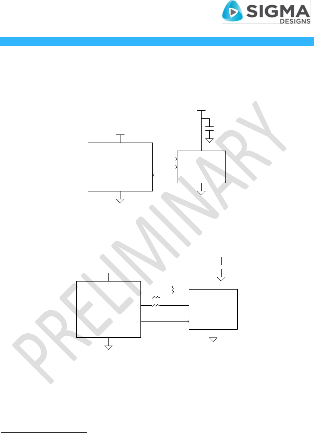
3 TYPICAL APPLICATION
An illustration of two application examples using the ZM5304 Modem implementation follows. The host application located on
an external microcontroller accesses the Z-Wave stack via the serial API. Figure 3.1 depicts the scenario when the UART is used
as the primary interface to the ZM5304 Modem, while Figure 3.2 shows the scenario when the USB
1
is used. It is strongly
recommended that the power supply is decoupled sufficiently, and a pull-up resistor placed on the RESET_N signal if the host
GPIO is unable to drive it.
ZM5304Host
RESET_N
RXD
TXD
GPIO
TXD
RXD
3V3
3V3
VDD
GND
Figure 3.1: Example of a host microcontroller based application using the UART
ZM5304Host
USB_DP
USB_DM
RESET_N
USB_DP
USB_DM
GPIO
3V3
3V3 3V3
1.5kΩ±5%
22Ω±5%
22Ω±5%
VDD
GND
Figure 3.2: Example of a host microcontroller based application using the USB
1
Firmware upgrades can be performed only when the ZM5304 Modem is placed in APM.
Datasheet: ZM5304
10 DSH12461-3 | 7/2013
4 PAD CONFIGURATION
The layout of the Exposed Pads (EP) on the ZM5304 Modem is shown in Figure 4.1.
10
9
8
7
6
5
4
3
2
1
48
47
46
45
44
43
42
41
40
39
38
37
36
35
11
12
13
14
15
16
17
18
19
20
21
22
23
24
B
O
A
R
D
C
U
T
O
U
T
25
26
27
28
29
30
31
32
33
34
GND
VDD
GND
USB_DP
USB_DM
RXD
TXD
NC
RESET_N
GND
GND
GND
GND
GND
NC
NC
NC
NC
GND
NC
GND
GND
NC
NC
NC
NC
NC
NC
NC
NC
NC
NC
NC
NC
NC
NC
NC
NC
NC
NC
NC
NC
NC
NC
NC
NC
GND
Plane
Copper
Free
GND
NC
Figure 4.1: Pad layout (top view)
4.1 PAD FUNCTIONALITY
Table 4.1: Power, ground, and no connect signals
Pad Name
Pad Location
Type2
Function
VDD
9
S
Module power supply.
GND
1, 8, 10, 11, 24, 25, 28, 30, 34, 35, 48
S
Ground. Must be connected to the ground
plane.
NC
3, 12, 13, 14, 15, 16, 17, 18, 19, 20, 21, 22, 23, 26, 27,
29, 31, 32, 33, 36, 37, 38, 39, 40, 41, 42, 43, 44, 45, 46,
47
-
Placement pads for mechanical stability.
Leave unconnected.
Table 4.2: Module control signals
Pad Name
Pad Location
Type
Function
RESET_N
2
I
Active low signal that places the module in
a reset state.
2
I = Input, O = Output, D+ = Differential Plus, D- = Differential Minus, S = Supply

Datasheet: ZM5304
DSH12461-3 | 7/2013 11
Table 4.3: UART interface signals
Pad Name
Pad
Location
Type
Function in Reset State
Function in Active State
RXD
5
I
Waits for the “Interface Enable” serial
command after 4.2ms. Enters ISP mode
after command is received from the host.
Receive data from host serial port.
TXD
4
O
Serial data transmit when in ISP mode,
high impedance otherwise.
Transmit data to host serial port.
Table 4.4: USB interface signals
Pad Name
Pad
Location
Type
Function in Reset State
Function in Active State
USB_DP
7
D+
USB 2.0 full speed APM when serial API
function is used before entering the reset
state.
USB 2.0 full speed.
USB_DM
6
D-
Datasheet: ZM5304
12 DSH12461-3 | 7/2013
5 ELECTRICAL CHARACTERISTICS
This section describes the electrical parameters of the ZM5304 Modem module.
5.1 TEST CONDITIONS
Final Test in Production
(TA=+25°C, VDD=+3.3V)
Characterization in Lab
(TA=-10°C to +85°C, VDD=+2.3 to +3.6V)
Statistics with Min,
Typ, and Max values
Sorting criterion
specified with Min and
Max values
Manufactured
Modules
Tested
Modules
Figure 5.1: Testing flow
The following conditions apply for characterization in the lab, unless otherwise noted.
1. Ambient temperature TA = -10 to +85°C
2. Supply voltage VDD = +2.3 to +3.6V
3. All tests are carried out on the ZDB5304 Z-Wave Development Board. [4]
4. Conducted transmission power is measured at the output of the SAW filter for 868.4, 908.4, 919.8, and 921.4MHz
5. Conducted receiver sensitivity is measure at the output of the SAW filter for 868.4, 908.4, 919.8, and 921.4MHz
The following conditions apply for the final test in production, unless otherwise noted.
1. Ambient temperature TA = +25°C
2. Supply voltage VDD = +3.3V
3. Radiated transmission power is measured for 868.4, 908.4, 919.8, and 921.4MHz
4. Radiated receiver sensitivity is measured for 868.4, 908.4, 919.8, and 921.4MHz
5.1.1 TYPICAL VALUES
Unless otherwise specified, typical data refer to the mean of a data set measured at an ambient temperature of TA=25°C and
supply voltage of VDD=+3.3V.
5.1.2 MINIMUM AND MAXIMUM VALUES
Unless otherwise specified the minimum and maximum values are guaranteed in the worst conditions of ambient temperature,
supply voltage and frequencies by a final test in production on 100% of the devices at an ambient temperature of TA=25°C and
supply voltage of VDD=+3.3V.
For data based on measurements, the minimum and maximum values represent the mean value plus or minus three times the
standard deviation (µ±3σ).

Datasheet: ZM5304
DSH12461-3 | 7/2013 13
5.2 ABSOLUTE MAXIMUM RATINGS
The absolute ratings specify the limits beyond which the module may not be functional. Exposure to absolute maximum
conditions for extended periods may cause permanent damage to the module.
Table 5.1: Voltage characteristics
Symbol
Description
Min
Max
Unit
VDD-GND
Main supply voltage
-0.3
+3.6
V
VIN-GND
Voltage applied on any I/O pad
-0.3
+3.6
V
ESDHBM
JEDEC JESD22-A114F Human Body Model
-
+2000.0
V
ESDMM
JEDEC JESD22-A115C Machine Model
-
+200.0
V
ESDCDM
JEDEC JESD22-C101E Field-Induced Charged-Device Model
-
+500.0
V
Table 5.2: Current characteristics
Symbol
Description
Min
Max
Unit
IVDD
Current into VDD power supply pad
-
+120
mA
IGND
Sum of the current out of all GND ground pads
-
-120
mA
Table 5.3: Thermal characteristics
Symbol
Description
Min
Max
Unit
TJ
Junction temperature
-55
+125
°C
5.3 GENERAL OPERATING RATINGS
The operating ratings indicate the conditions where the module is guaranteed to be functional.
Table 5.4: Recommended operating conditions
Symbol
Description
Min
Typ
Max
Unit
VDD
Standard operating supply voltage
+2.3
+3.3
+3.6
V
VDD_USB
Standard operating supply voltage when USB PHY is used
+3.0
+3.3
+3.6
V
fSYS
Internal clock frequency
-
32.0
-
MHz
TA
Ambient operating temperature
-10.0
+25.0
+85.0
°C
5.4 CURRENT CONSUMPTION
Measured at an ambient temperature of TA=+25°C and a supply voltage of VDD=+3.3V.
Datasheet: ZM5304
14 DSH12461-3 | 7/2013
Table 5.5: Current consumption in active modes
Symbol
Description
Min
Typ
Max
Unit
IDD_ACTIVE
MCU running at 32MHz
-
15
16
mA
IDD_ACTIVE_USB
MCU running at 32MHz and USB PHY active
-
TBD
TBD
mA
IDD_RX
MCU and radio receiver active
-
32
34
mA
IDD_TX_0
MCU and radio transmitter active, 0dBm
-
36
TBD
mA
IDD_TX_2
MCU and radio transmitter active, +2dBm
-
40
TBD
mA
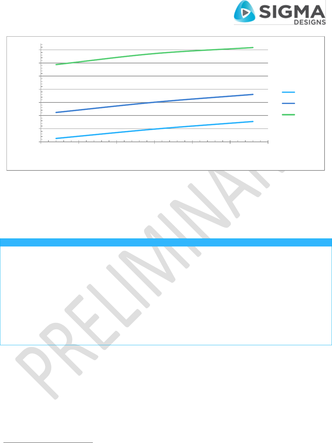
Figure 5.2: Typical current consumption vs. transmit power
Table 5.6: Current consumption in power saving modes
Symbol
Description
Min
Typ
Max
Unit
IDD_SLEEP
Module in sleep state
-
2.0
TBD
µA
IUSB_SLEEP
USB suspend mode with state persistency, and system clock
(Measured at an ambient temperature of TA=-10°C to +85°C
and a supply voltage of VDD=+2.3V to +3.6V)
-
2.0
2.3
mA
Table 5.7: Current consumption during programming
Symbol
Description
Min
Typ
Max
Unit
IDD_PGM_UART
Programming via UART
TBD
15
TBD
mA
IDD_PGM_USB
Programming via USB
TBD
15
TBD
mA
5.5 SYSTEM TIMING
Measured at an ambient temperature of TA=-10°C to +85°C and a supply voltage of VDD=+2.3V to +3.6V.
27
29
31
33
35
37
39
41
43
-27 -24 -21 -18 -15 -12 -9 -6 -3 0 3
Current Consumption (mA)
Transmit Power (dBm)

Datasheet: ZM5304
DSH12461-3 | 7/2013 15
Table 5.8: Transition between operating modes
Symbol
Description
Min
Typ
Max
Unit
tACTIVE_SLEEP
Transition time from the active state to the sleep state
-
-
125
ns
tSLEEP_ACTIVE
Transition time from the sleep state to the active state ready
to execute code
160
-
-
µs
Table 5.9: System start-up time
Symbol
Description
Min
Typ
Max
Unit
VPOR
Power-on-Reset (POR) threshold on rising supply voltage at
which the reset signal is deasserted
-
-
+2.3
V
tRESET_ACTIVE
Transition time from the reset state to the active state ready
to execute code with a power rise time not exceeding 10µs
-
-
1.0
ms
Table 5.10: Reset timing requirements
Symbol
Description
Min
Typ
Max
Unit
tRST_PULSE
Duration to assert RESET_N to guarantee a full system reset
20
-
-
ns
Table 5.11: Programming time
Symbol
Description
Min
Typ
Max
Unit
tERASE_FULL
Time taken to erase the entire flash memory
-
-
44.1
ms
tPGM_FULL
Time taken to program the entire flash memory
TBD
TBD
TBD
ms
5.6 NON-VOLATILE MEMORY RELIABILITY
Qualified for an ambient temperature of TA=+25°C and a supply voltage of VDD=+3.3V. The on-chip memory is based on
SuperFlash® technology.
Table 5.12: On-chip flash
Symbol
Description
Min
Typ
Max
Unit
ENDFLASH
Endurance, erase cycles before failure
10000
-
-
cycles
RETFLASH-LT
Data retention
100
-
-
years
RETFLASH-HT
Data retention (Qualified for a junction temperature of
TJ=-10°C to +85°C)
10
-
-
years
Table 5.13: EEPROM
Symbol
Description
Min
Typ
Max
Unit
ENDEEPROM
Endurance, erase cycles before failure
1Mil
-
-
cycles
RETEEPROM
Data retention
100
-
-
years

Datasheet: ZM5304
16 DSH12461-3 | 7/2013
5.7 ANALOG-TO-DIGITAL CONVERTER
Measured at an ambient temperature of TA=-10°C to +85°C and a supply voltage of VDD=+2.3V to +3.6V.
Table 5.14: 12 bit ADC characteristics
Symbol
Description
Min
Max
Unit
VBG
Internal reference voltage
+1.20
+1.30
V
VREF+
Upper reference input voltage
VDD - 0.90
VDD
V
VREF-
Lower reference input voltage
0.00
+1.20
V
DNLADC
Differential non-linearity
-1.00
+1.00
LSB
ACC8b
Accuracy when sampling 20ksps with 8 bit resolution
-2.00
2.00
LSB
ACC12b
Accuracy when sampling 10ksps with 12 bit resolution
-5.00
5.00
LSB
fS-8b
8 bit sampling rate
-
0.02
Msps
fS-12b
12 bit sampling rate
-
0.01
Msps
5.8 DC CHARACTERISTICS
Measured at an ambient temperature of TA=-10°C to +85°C.
Table 5.15: Digital input characteristics, supply voltage of VDD=+2.3V to +3.0V
Symbol
Description
Min
Max
Unit
VIH
Logical 1 input voltage high level
+1.85
-
V
VIL
Logical 0 input voltage low level
-
+0.75
V
VIF
Falling input trigger threshold
+0.75
+1.05
V
VIR
Rising edge trigger threshold
+1.35
+1.85
V
VHYS
Schmitt trigger voltage hysteresis
+0.55
+0.85
V
IIH
Logical 1 input high level current leakage
-
+7.00
µA
IIL-NPU
Logical 0 input low level current leakage (no internal pull-up resistor)
-
-7.00
µA
IIL-PU
Logical 0 input low level current leakage (with internal pull-up resistor)
+35.00
+90.00
µA
CIN
Pad input capacitance
-
15.00
pF
Table 5.16: Digital output characteristics, supply voltage of VDD=+2.3V to +3.0V
Symbol
Description
Min
Max
Unit
VOH
Logical 1 output voltage high level
+1.9
-
V
VOL
Logical 0 output voltage low level
-
+0.4
V
IOH-LP
Logical 1 output high level current sourcing
+6.0
mA
IOL-LP
Logical 0 output low level current sinking
-6.0
mA

Datasheet: ZM5304
DSH12461-3 | 7/2013 17
Table 5.17: Digital input characteristics, supply voltage of VDD=+3.0V to +3.6V
Symbol
Description
Min
Max
Unit
VIH
Logical 1 input voltage high level
+2.10
-
V
VIL
Logical 0 input voltage low level
-
+0.90
V
VIF
Falling input trigger threshold
+0.90
+1.30
V
VIR
Rising edge trigger threshold
+1.60
+2.10
V
VHYS
Schmitt trigger voltage hysteresis
+0.65
+0.95
V
IIH
Logical 1 input high level current leakage
-
+10.00
µA
IIL-NPU
Logical 0 input low level current leakage (no internal pull-up resistor)
-
-10.00
µA
IIL-PU
Logical 0 input low level current leakage (with internal pull-up resistor)
+40.00
+120.00
µA
CIN
Pad input capacitance
-
15.00
pF
Table 5.18: Digital output characteristics, supply voltage of VDD=+3.0V to +3.6V
Symbol
Description
Min
Max
Unit
VOH
Logical 1 output voltage high level
+2.4
-
V
VOL
Logical 0 output voltage low level
-
+0.4
V
IOH-LP
Logical 1 output high level current sourcing
-
+8.0
mA
IOL-LP
Logical 0 output low level current sinking
-
-8.0
mA
5.9 RF CHARACTERISTICS
5.9.1 TRANSMITTER
Measured at an ambient temperature of TA=-10°C to +85°C and a supply voltage of VDD=+2.3V to +3.6V. The transmission power
is adjusted by setting the value of the RFPOW register.
Table 5.19: Transmit performance
Symbol
Description
Min
Typ
Max
Unit
P63
RF output power delivered to the antenna, RFPOW=63
+1.3
+2.0
+3.5
dBm
P01
RF output power delivered to the antenna, RFPOW=01
-27.5
-26.3
-25.0
dBm
PH2
2nd harmonic, RFPOW=63
TBD
dBc
PH3
3rd harmonic, RFPOW=63
TBD
dBc
Datasheet: ZM5304
18 DSH12461-3 | 7/2013
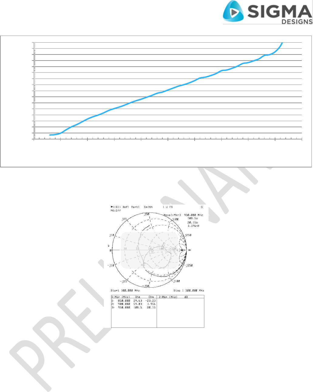
Figure 5.3: Typical transmit power vs. RFPOW setting
Figure 5.4: Typical output impedance
5.9.2 RECEIVER
Measured over an ambient temperature of TA=-10°C to +85°C and a supply voltage of VDD=+2.3V to +3.6V.
Table 5.20: Receiver sensitivity
Symbol
Description
Min
Typ
Max
Unit
P9.6
Sensitivity at 9.6kbps, FER < 1%
-
-103
-
dBm
P40
Sensitivity at 40kbps, FER < 1%
-
-99
-
dBm
P100
Sensitivity at 100kbps, FER < 1%
-
-92
-
dBm
-27
-24
-21
-18
-15
-12
-9
-6
-3
0
3
0 5 10 15 20 25 30 35 40 45 50 55 60
Transmit Power (dBm)
RFPOW Setting
TBD
Datasheet: ZM5304
DSH12461-3 | 7/2013 19
Figure 5.5: Typical sensitivity vs. temperature
Measured at an ambient temperature of TA=+25°C and a supply voltage of VDD=+3.3V.
Table 5.21: Receiver performance
Symbol
Description
Min
Typ
Max
Unit
CCR
Co-channel rejection
-
TBD
-
dBc
ACR200kHz
Adjacent channel rejection at Δf=200kHz
-
TBD
-
dBc
ACR400kHz
Adjacent channel rejection at Δf=400kHz
-
TBD
-
dBc
ACR800kHz
Adjacent channel rejection at Δf=800kHz
-
TBD
-
dBc
BI1MHZ
Blocking immunity3 at Δf=1MHz
-
34.0
-
dBc
BI2MHZ
Blocking immunity at Δf=2MHz
-
38.0
-
dBc
BI5MHZ
Blocking immunity at Δf=5MHz
-
60.0
-
dBc
BI10MHZ
Blocking immunity at Δf=10MHz
-
63.0
-
dBc
BI100MHZ
Blocking immunity at Δf=100MHz
-
TBD
-
dBc
RSSIRANGE
Dynamic range of the RSSI measurement
-
70.0
-
dB
RSSILSB
Resolution of the RSSI measurement
-
1.5
-
dB
PLO
LO leakage at Δf=TBDkHz
-
-80.0
-
dBm
IIP3
Input 3rd order intercept point
-
-12.0
-
dBm
3
Blocker level is defined relative to the wanted receiving signal and measured with the wanted receiving signal 3dB above the
sensitivity level
-105
-103
-101
-99
-97
-95
-93
-91
-50 -25 0 25 50 75 100
Sensitivity (dBm)
Temperature (°C)
9.6 kbps
40 kbps
100 kbps
Datasheet: ZM5304
20 DSH12461-3 | 7/2013
Figure 5.6: Typical input power vs. RSSI value
Figure 5.7: Typical input impedance
-110
-105
-100
-95
-90
-85
-80
-75
-70
-65
-60
-55
-50
-45
-40
-35
-30
35 40 45 50 55 60 65 70 75 80 85
Received Power (dBm)
Received Signal Strength Indicator Value
TBD
Datasheet: ZM5304
DSH12461-3 | 7/2013 21
5.9.3 ANTENNA
Figure 5.8: Radiatian pattern measured starting from the top
with the antenna placed to the left on the ZX plane
Figure 5.9: Radiatian pattern measured starting from the top
with the antenna facing up on the XY plane
Figure 5.10: Radiation pattern measured starting from the right with the antenna placed to the left on the YZ plane

Datasheet: ZM5304
22 DSH12461-3 | 7/2013
Table 5.22: Antenna performance
Frequency Range (MHz)
Orientation
Average Gain (dBi)
Max Gain (dBi)
Total Efficiency (%)
868
XY plane, horizontal
-11.6
-9.4
34.6
XY plane, vertical
-5.4
-4.6
YZ plane, horizontal
-6.2
-2.8
YZ plane, vertical
-14.3
-12.6
ZX plane, horizontal
-7.3
-4.4
ZX plane, vertical
-8.4
-6.8
908
XY plane, horizontal
-11.6
-9.4
31.6
XY plane, vertical
-5.5
-4.7
YZ plane, horizontal
-6.8
-3.5
YZ plane, vertical
-14.5
-13.2
ZX plane, horizontal
-8.0
-5.1
ZX plane, vertical
-8.6
-7.4
923.5
XY plane, horizontal
-11.9
-9.7
36.3
XY plane, vertical
-4.9
-4.0
YZ plane, horizontal
-6.2
-2.9
YZ plane, vertical
-13.9
-12.7
ZX plane, horizontal
-7.3
-4.3
ZX plane, vertical
-8.3
-7.1
5.9.4 REGULATORY COMPLIANCE
The ZM5304 Modem has been tested to be compliant with the following regulatory standards.
ACMA COMPLIANCE
o AS/NZS 4268
o CISPR 22
CE COMPLIANCE
o EN 50364
o EN 60950
o EN 300 220
o EN 301 489-1/3
FCC COMPLIANCE
o FCC CFR 47 Part 15 Unlicensed Modular Approval
IC COMPLIANCE
o RSS-GEN
o RSS-210
MIC COMPLIANCE
o ARIB STD-T108

Datasheet: ZM5304
DSH12461-3 | 7/2013 23
6 Z-WAVE FREQUENCIES
Table 6.1: Z-Wave RF specification
Data rate
9.6kbps
40kbps
100kbps
Modulation
Frequency Shift Keying (FSK)
FSK
Gaussian Frequency Shift Keying (GFSK)
Frequency deviation
fC±20kHz
fC±20kHz
fC±29.3kHz
Coding
Manchester encoded
Non-return to Zero (NRZ)
NRZ
United Arab Emirates
868.42 MHz
868.40 MHz
869.85 MHz
E
Australia
921.42 MHz
921.40 MHz
919.80 MHz
H
Brazil
921.42 MHz
921.40 MHz
919.80 MHz
H
Canada
908.42 MHz
908.40 MHz
916.00 MHz
U
Chile
908.42 MHz
908.40 MHz
916.00 MHz
U
China
868.42 MHz
868.40 MHz
869.85 MHz
E
European Union
868.42 MHz
868.40 MHz
869.85 MHz
E
Hong Kong
919.82 MHz
919.80 MHz
919.80 MHz
H
Israel
916.02 MHz
916.00 MHz
-
U
India
865.20 MHz
865.20 MHz
865.20 MHz
E
Japan
-
-
922.50 MHz
H
-
-
923.90 MHz
H
-
-
926.30 MHz
H
Korea
-
-
919.70 MHz
H
-
-
923.10 MHz
H
-
-
926.30 MHz
H
Mexico
908.42 MHz
908.40 MHz
916.00 MHz
U
Malaysia
868.12 MHz
868.10 MHz
868.10 MHz
E
New Zealand
921.42 MHz
921.40 MHz
919.80 MHz
H
Russia
869.02 MHz
869.00 MHz
-
E
Singapore
868.42 MHz
868.40 MHz
869.85 MHz
E
Taiwan
-
-
922.50 MHz
H
-
-
923.90 MHz
H
-
-
926.30 MHz
H
United States
908.42 MHz
908.40 MHz
916.00 MHz
U
South Africa
868.42 MHz
868.40 MHz
869.85 MHz
E
Datasheet: ZM5304
24 DSH12461-3 | 7/2013
7 MODULE INFORMATION
7.1 MODULE MARKING
A
N
T
E
N
N
A
FCC ID
REGION
Figure 7.1: Marking placement
Table 7.1: Marking description
Regional information
REGION:
E
U
H
US regulatory information
FCC ID
NB: The shield is mounted only on the U regional module.
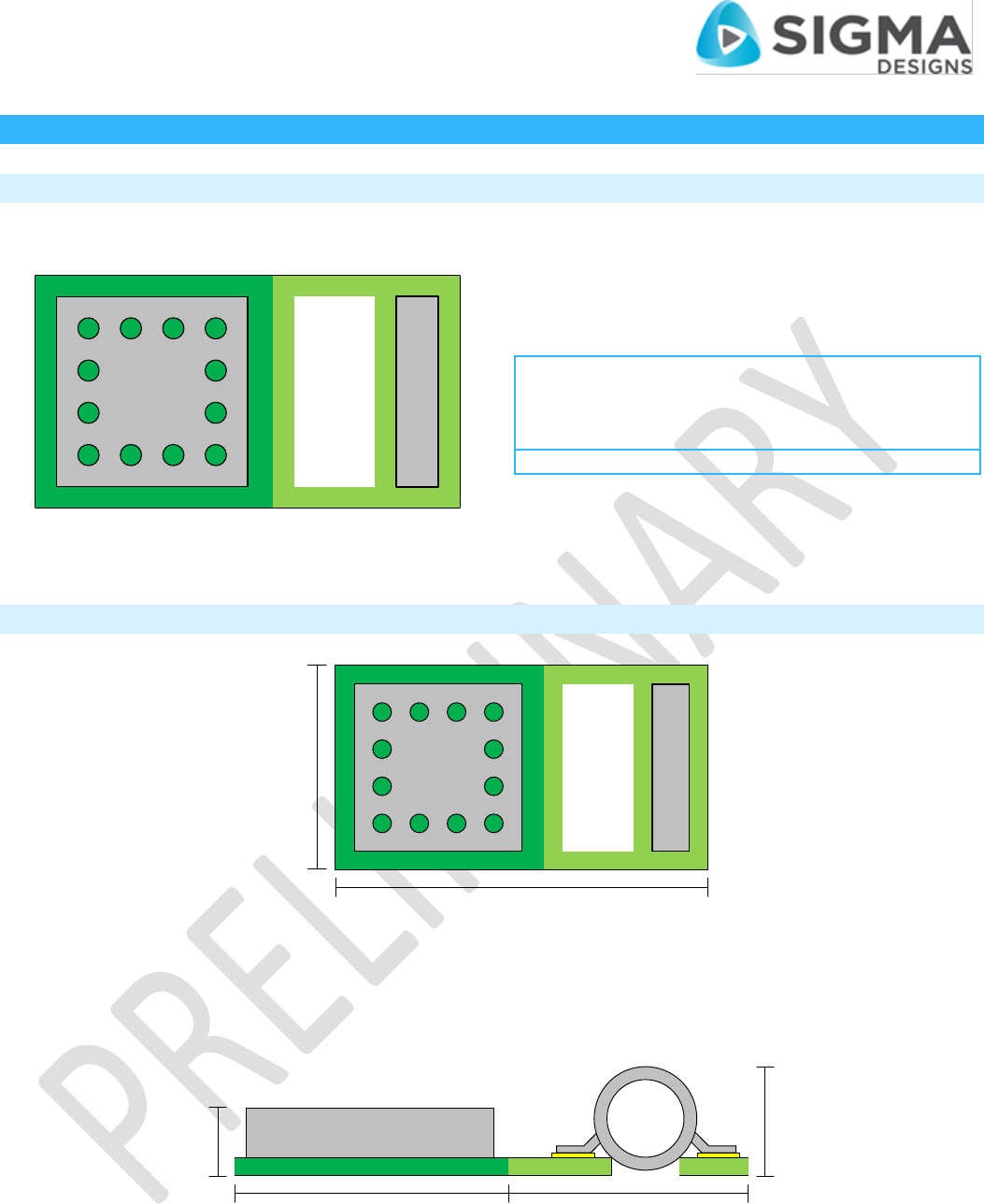
7.2 MODULE DIMENSIONS
* All dimensions are in millimeters (mm)
0
15.20
0
27
A
N
T
E
N
N
A
Shield
ZM5304 vHW/vFW
PRODCODE
YYWWDD
FCC ID: TBD
A
N
T
E
N
N
A
FCC ID
REGION
Figure 7.2: Top view of module
Shield
PAD
* All dimensions are in millimeters (mm)
PAD
ANTENNA
GND Plane Copper Free Copper Free
27
0
0
5.5
0
3.8
15
Figure 7.3: Side view of module
Datasheet: ZM5304
DSH12461-3 | 7/2013 25
8 PCB MOUNTING AND SOLDERING
8.1 RECOMMENDED PCB MOUNTING PATTERN
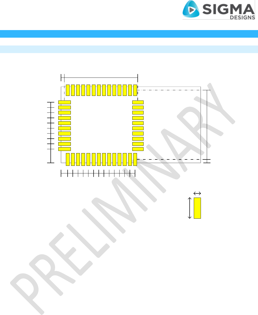
0.65
1.70
* All dimensions are in millimeters (mm)
P
A
D
3.10 10
4.10 9
5.10 8
6.10 7
7.10 6
8.10 5
9.10 4
10.10 3
11.10 2
12.10 1
48
47
46
45
44
43
42
41
40
39
38
37
36
35
111
212
313
414
515
616
717
818
919
10 20
11 21
12 22
13 23
14 24
25
26
27
28
29
30
31
32
33
34
0
0
15.05
0
0.15
0
14.85
0.15
Top View
Figure 8.1: Top view of land pattern
Datasheet: ZM5304
26 DSH12461-3 | 7/2013
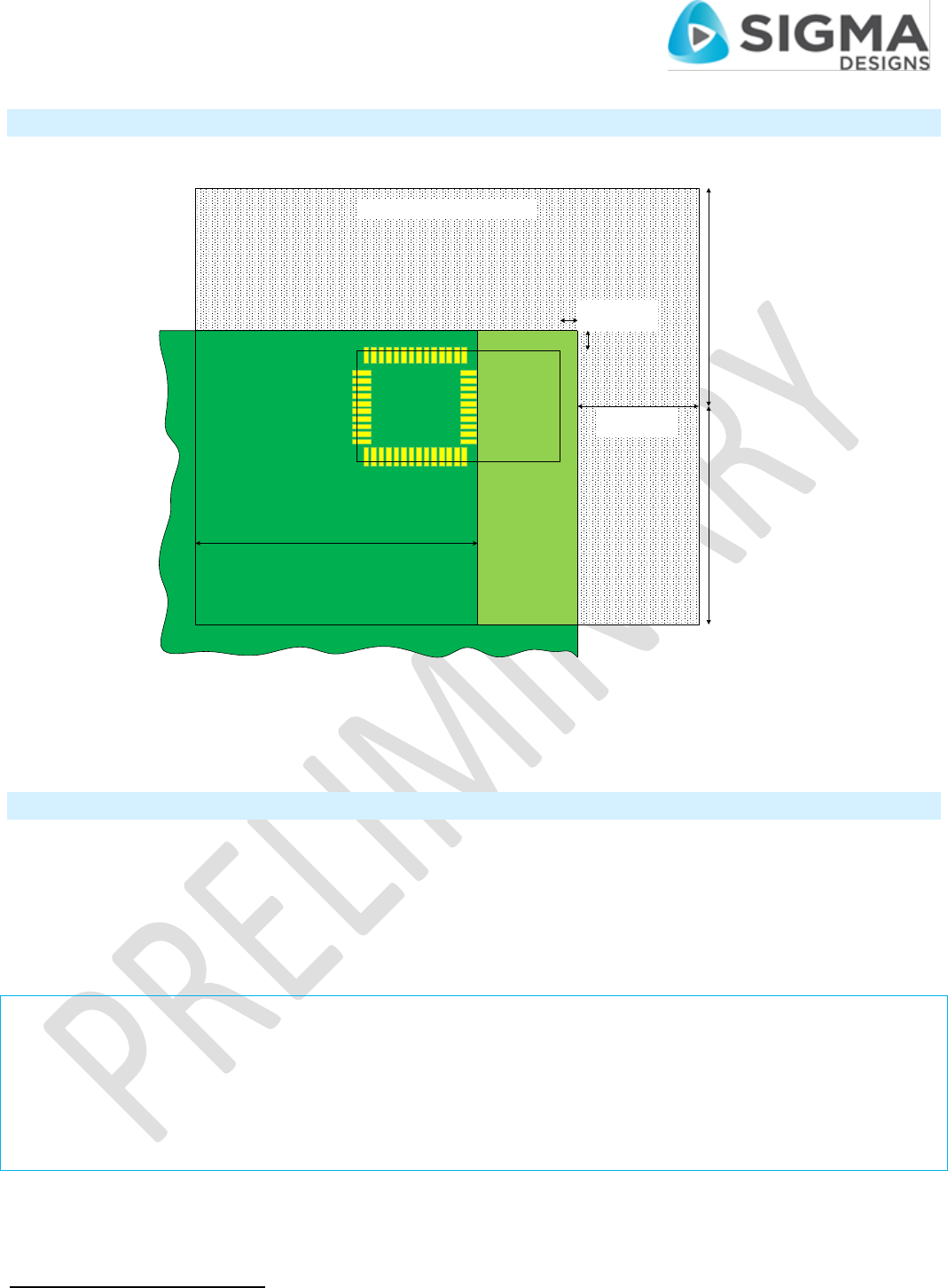
8.2 RECOMMENDED PLACEMENT ON PCB
> 55mm
recommended
10
9
8
7
6
5
4
3
2
1
48
47
46
45
44
43
42
41
40
39
38
37
36
35
11
12
13
14
15
16
17
18
19
20
21
22
23
24
25
26
27
28
29
30
31
32
33
34
> 5mm
recommended
> 50mm
recommended
PCB ground plane with components Copper free PCB
Recommended metal free space
> 55mm
recommended
> 50mm
recommended
Figure 8.2: Top view of recommended placement of module on PCB
8.3 SOLDERING INFORMATION
The soldering details to properly solder the ZM5202 module on standard PCBs are described below. The information provided is
intended only as a guideline and Sigma Designs is not liable if a selected profile does not work.
See IPC/JEDEC J-STD-020D.1 for more information.
Table 8.1: Soldering details
PCB solder mask expansion from landing pad edge
0.1 mm
PCB paste mask expansion from landing pad edge
0 mm
PCB process
Pb-free (Lead free for RoHS 4compliance)
PCB finish
Defined by the manufacturing facility (EMS) or customer
Stencil aperture
Defined by the manufacturing facility (EMS) or customer
Stencil thickness
Defined by the manufacturing facility (EMS) or customer
Solder paste used
Defined by the manufacturing facility (EMS) or customer
Flux cleaning process
Defined by the manufacturing facility (EMS) or customer
4
RoHS = Restriction of Hazardous Substances Directive, EU
Datasheet: ZM5304
DSH12461-3 | 7/2013 27
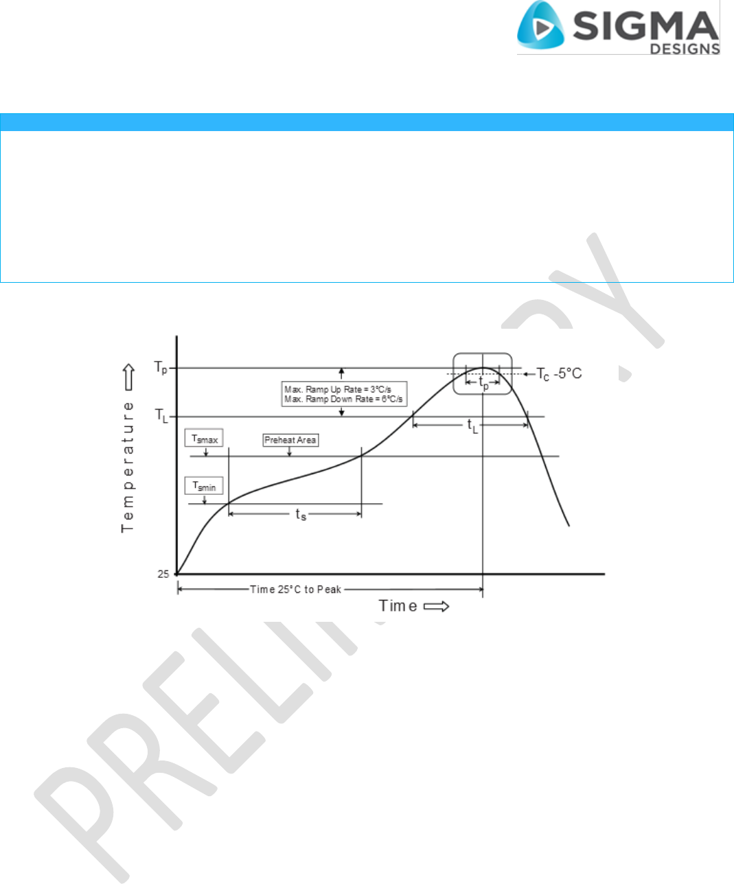
Table 8.2: Typical reflow profile
Symbol
Description
Min
Max
Unit
TP to TL
Ramp-up rate
-
3
°C/s
TS
Preheat temperature
150
200
°C
tS
Preheat time
60
120
s
TL
Heating temperature
215
220
°C
tL
Heating time
60
150
s
TP
Peak temperature
-
260
°C
tP
Time within 5°C of actual peak temperature
28
32
s
TP to TL
Ramp-down rate
-
6
°C/s
t
Time 25°C to peak temperature
-
8
min
Figure 8.3: Typical reflow profile

Datasheet: ZM5304
28 DSH12461-3 | 7/2013
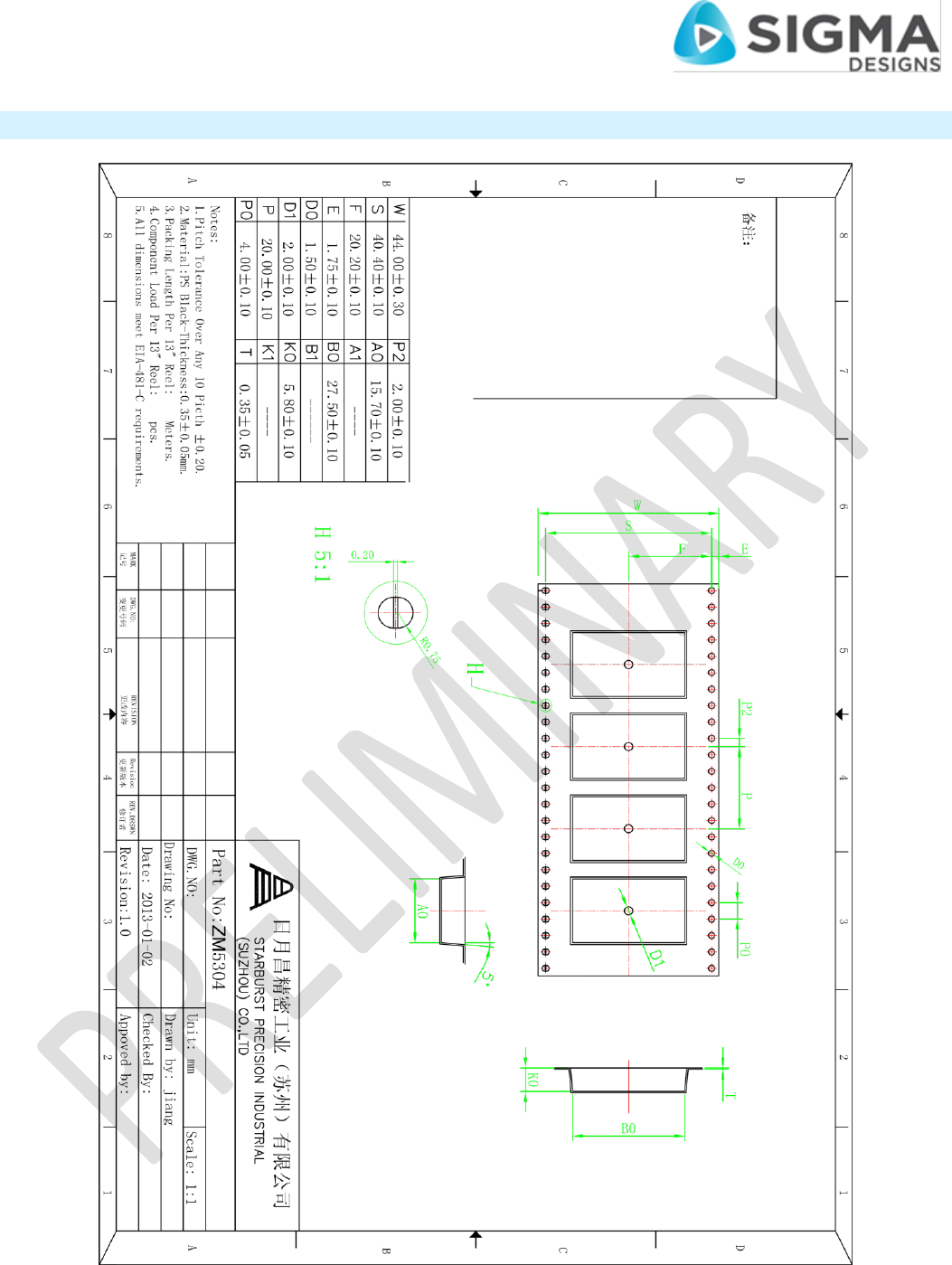
9 ORDERING INFORMATION
Table 9.1: Ordering codes
Orderable Device
Status
Package
Type
Pads
Minimum Order
Quantity
Description
ZM5304AE-CME3R
ACTIVE
SOM5
48
500 pcs.
ZM5304 Modem Module, No Shield, RevA,
868MHz Band, Tape and Reel
ZM5304AU-CME3R
ACTIVE
SOM
48
500 pcs.
ZM5304 Modem Module, With Shield, RevA,
908MHz Band, Tape and Reel
ZM5304AH-CME3R
ACTIVE
SOM
48
500 pcs.
ZM5304 Modem Module, No Shield, RevA,
921MHz Band, Tape and Reel
5
SOM = System-on-Module
Datasheet: ZM5304
DSH12461-3 | 7/2013 29
9.1 TAPE AND REEL INFORMATION
Figure 9.1: Tape information
Datasheet: ZM5304
30 DSH12461-3 | 7/2013
Figure 9.2: Reel information

Datasheet: ZM5304
DSH12461-3 | 7/2013 31
10 REVISION HISTORY
Date
Version
Affected
Revision
2013/07/02
3A
§1, §2, §5
Removed remnants of WUT
TODO:
Add table of abbreviations
Add typical IO graphs
2013/07/02
2B
§2.1.9, §10
Remove invalid references to the WUT and added the date to
the references, with feedback from NTJ, MVO, and OPP
2013/07/01
2A
§2.1, §2.3, §7.2, §6
Added dimensions of shield
Changed the low operating voltage from 2.5V to 2.3V
Added AES, ADC, XTAL driver, BOD, RST controller, WUT,
Watchdog, and RF transceiver sections to the peripheral
descriptions
Changed “Firmware Upgrade” to “Module Programming” and
added default programming mode
Changed the module width to 15.05mm
Removed the frequency from the module marking and added
region data to the frequency table
TODO:
Add table of abbreviations
Add typical IO graphs
2013/06/03
1F
§5.5, §6
Added transition time values
Removed empty page
TODO:
Add table of abbreviations
Add typical IO graphs
2013/05/31
1E
§All
Updated IO characteristics and added USB termination
resistor values
TODO:
Verify USB 2.0 vs. 1.1
Add table of abbreviations
Add typical IO graphs
2013/05/30
1D
§All
Updated with feedback from MVO and NTJ.
Added missing receiver graphs.
TODO:
Verify USB termination resistor values
Verify USB 2.0 vs. 1.1
Add table of abbreviations
2013/05/27
1C
§All
Updated layout with feedback from Jeanne Christiansen, and
data from the latest corner tests.
2013/02/22
1A
§All
Preliminary draft released.
2013/02/18
1A
§All
Initial draft.

Datasheet: ZM5304
32 DSH12461-3 | 7/2013
11 REFERENCES
[1] Sigma Designs, “Serial API Host Application Programming Guide,” INS12350, Denmark, 2012.
[2] Sigma Designs, “Z-Wave 500 Series Application Programmers Guide v6.50.00,” INS12308, Denmark, 2012.
[3] Sigma Designs, “500 Series Z-Wave Single Chip Programming Mode,” INS11681, Denmark, 2012.
[4] Sigma Designs, “ZDB5304 Z-Wave Development Board,” DSH12468, Denmark, 2013.

Datasheet: ZM5304
DSH12461-3 | 7/2013 33
DISCLAIMER
The information in this document is subject to change without notice. Sigma Designs reserves the right to make changes in
circuit design and/or specifications at any time without notice. Accordingly, the reader is cautioned to verify that the datasheet
is current before placing orders. Information furnished by Sigma Designs is believed to be accurate and reliable. However, no
responsibility is assumed by Sigma Designs or its subsidiaries for its use; nor for any infringements of patents or other rights of
third parties, which may result from its use. No license is granted by implication or otherwise under any patent or patent rights
of Sigma Designs or its subsidiaries.
Sigma Designs, Inc. makes no warranty, express, statutory, implied or by description, regarding the information set forth herein
or regarding the freedom of the described devices from intellectual property infringement. Sigma Designs, Inc. makes no
warranty of merchantability or fitness for any purpose.
Sigma Designs, Inc. shall not be responsible for any errors that may appear in this document. Sigma Designs, Inc. makes no
commitment to update or keep current the information contained in this document.
The product(s) described in this document is not intended for use as critical component(s) in life support devices or systems
without prior written permission from Sigma Designs, Inc.
No part of this document may be copied or reproduced in any form or by any means without the prior written consent of Sigma
Designs, Inc. The information in this document is subject to change without notice. Sigma Designs logo are either registered
trademarks or trademarks of Sigma Designs, Inc. in the United States and/or other countries. All other trademarks or registered
trademarks are the property of their respective owners.
Sigma Designs products are sold by description only. Sigma Designs reserves the right to make changes in circuit design and/or
specifications at any time without notice. Accordingly, the reader is cautioned to verify that data sheets are current before
placing orders. Information furnished by Sigma Designs is believed to be accurate and reliable. However, no responsibility is
assumed by Sigma Designs or its subsidiaries for its use; nor for any infringements of patents or other rights of third parties,
which may result from its use. No license is granted by implication or otherwise under any patent or patent rights of Sigma
Designs or its subsidiaries.
CONFIDENTIALITY
This document contains confidential information, trade secrets, or both that are the property of Sigma Designs, Inc. It is to be
treated as confidential under the Non-Disclosure Agreement (NDA), which has been signed by the obtainer. Reproduction or
transmission in any manner to others in whole or in part is prohibited without prior written permission from Sigma Designs, Inc.
TRADEMARKS
Sigma Designs and the Sigma Designs logo are registered trademarks of Sigma Designs, Inc. in the United States and/or other
countries. All other trademarks or registered trademarks are the properties of their respective owners.
Z-Wave® is a registered trademark of Sigma Designs, Inc. in the United States and/or other countries.
SALES OFFICE AND DISTRIBUTOR CONTACT INFORMATION
www.sigmadesigns.com/sales
HEADQUARTERS
Sigma Designs, Inc.
1778 McCarthy Blvd. Milpitas, CA 95035
Tel: +1.408.262.9003 Fax: +1.408.957.9740
www.sigmadesigns.com
sales@sigmadesigns.com
Federal Communication Commission Interference Statement
This device complies with Part 15 of the FCC Rules. Operation is subject to
the following two conditions: (1) This device may not cause harmful
interference, and (2) this device must accept any interference received,
including interference that may cause undesired operation.
This equipment has been tested and found to comply with the limits for a
Class B digital device, pursuant to Part 15 of the FCC Rules. These limits
are designed to provide reasonable protection against harmful interference in a
residential installation. This equipment generates, uses and can radiate radio
frequency energy and, if not installed and used in accordance with the
instructions, may cause harmful interference to radio communications.
However, there is no guarantee that interference will not occur in a particular
installation. If this equipment does cause harmful interference to radio or
television reception, which can be determined by turning the equipment off
and on, the user is encouraged to try to correct the interference by one of the
following measures:
- Reorient or relocate the receiving antenna.
- Increase the separation between the equipment and receiver.
- Connect the equipment into an outlet on a circuit different from that
to which the receiver is connected.
- Consult the dealer or an experienced radio/TV technician for help.
FCC Caution: Any changes or modifications not expressly approved by the
party responsible for compliance could void the user's authority to operate this
equipment.
This transmitter must not be co-located or operating in conjunction with any
other antenna or transmitter.

This device is intended only for OEM integrators under the following conditions:
1) The antenna must be installed such that 20 cm is maintained between the
antenna and users, and
2) The transmitter module may not be co-located with any other transmitter or
antenna.
As long as 2 conditions above are met, further transmitter test will not be
required. However, the OEM integrator is still responsible for testing their
end-product for any additional compliance requirements required with this
module installed
IMPORTANT NOTE: In the event that these conditions can not be met (for
example certain laptop configurations or co-location with another transmitter),
then the FCC authorization is no longer considered valid and the FCC ID can
not be used on the final product. In these circumstances, the OEM integrator will
be responsible for re-evaluating the end product (including the transmitter) and
obtaining a separate FCC authorization.
End Product Labeling
This transmitter module is authorized only for use in device where the antenna
may be installed such that 20 cm may be maintained between the antenna and
users. The final end product must be labeled in a visible area with the following:
“Contains FCC ID: D87-ZM5304-U”. The grantee's FCC ID can be used only
when all FCC compliance requirements are met.
Manual Information To the End User
The OEM integrator has to be aware not to provide information to the end user
regarding how to install or remove this RF module in the user’s manual of the
end product which integrates this module.
The end user manual shall include all required regulatory information/warning as
show in this manual.