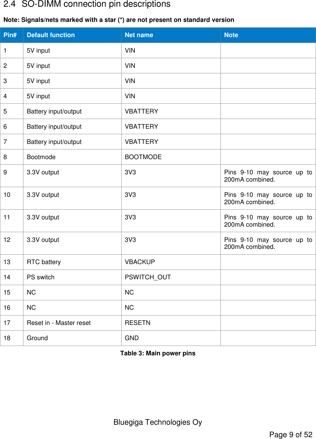
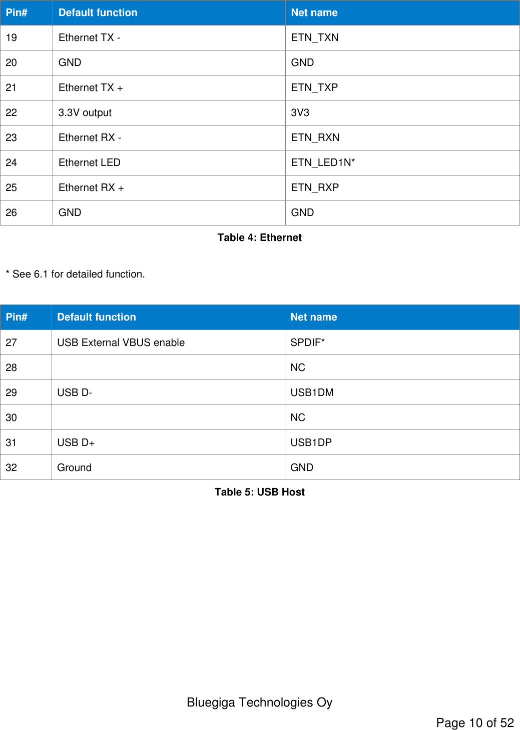
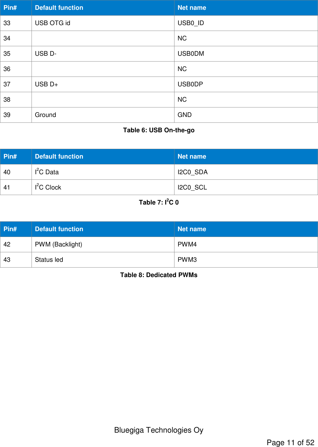
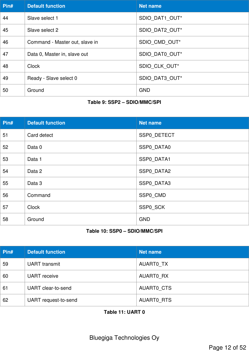
Silicon Laboratories Finland APX4 Wireless System-on-Module User Manual APx4 datasheet
Silicon Laboratories Finland Oy Wireless System-on-Module APx4 datasheet
UserManual.wiki
>
Silicon Laboratories Finland
>
APX4 User Manual
Datasheet
Navigation menu
Upload a User Manual
Namespaces
Wiki Guide
HTML
PDF
Info
Views
User Manual
Discussion / Help
Navigation
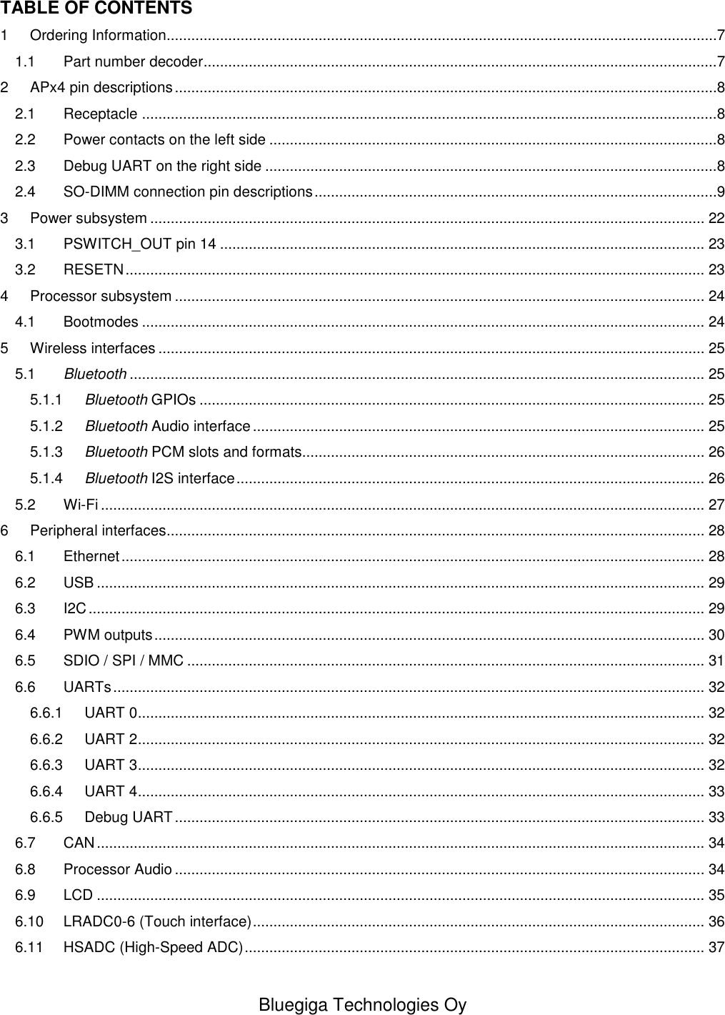
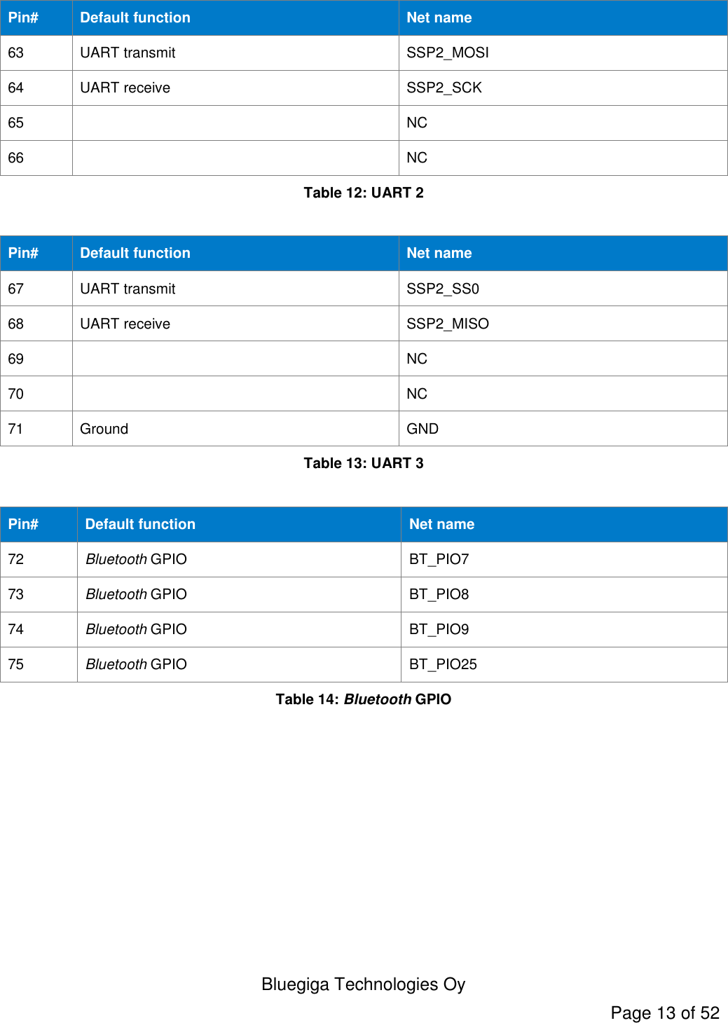
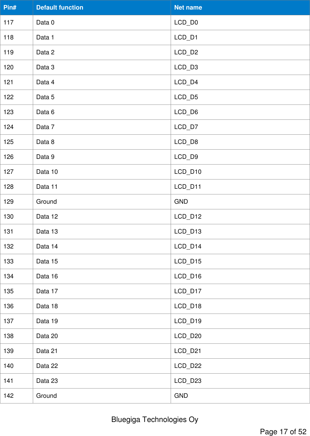
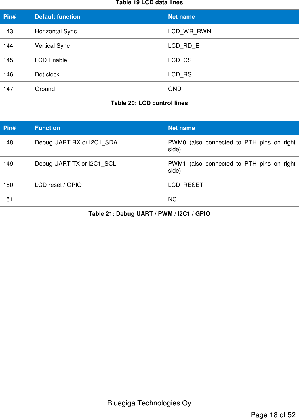
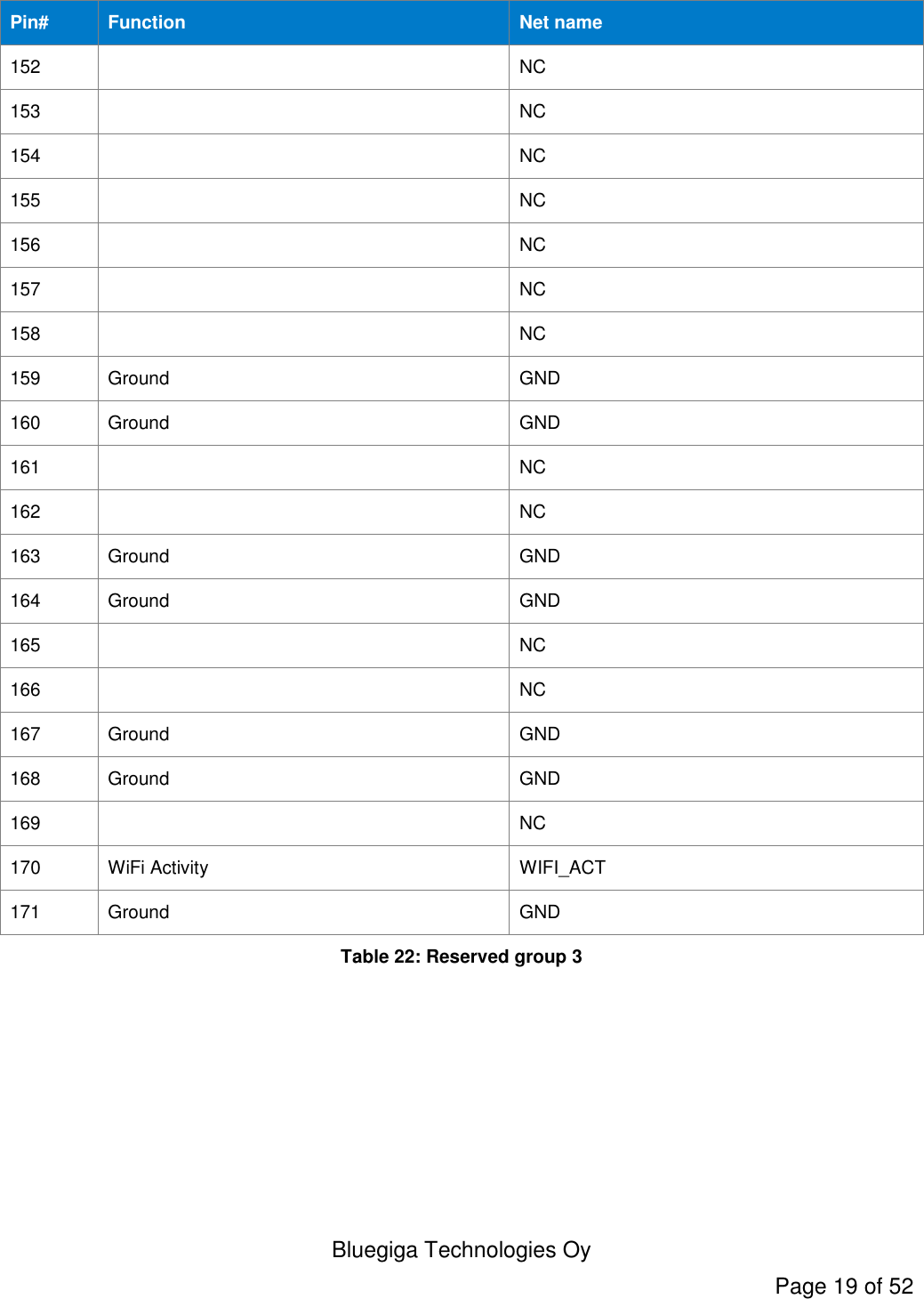
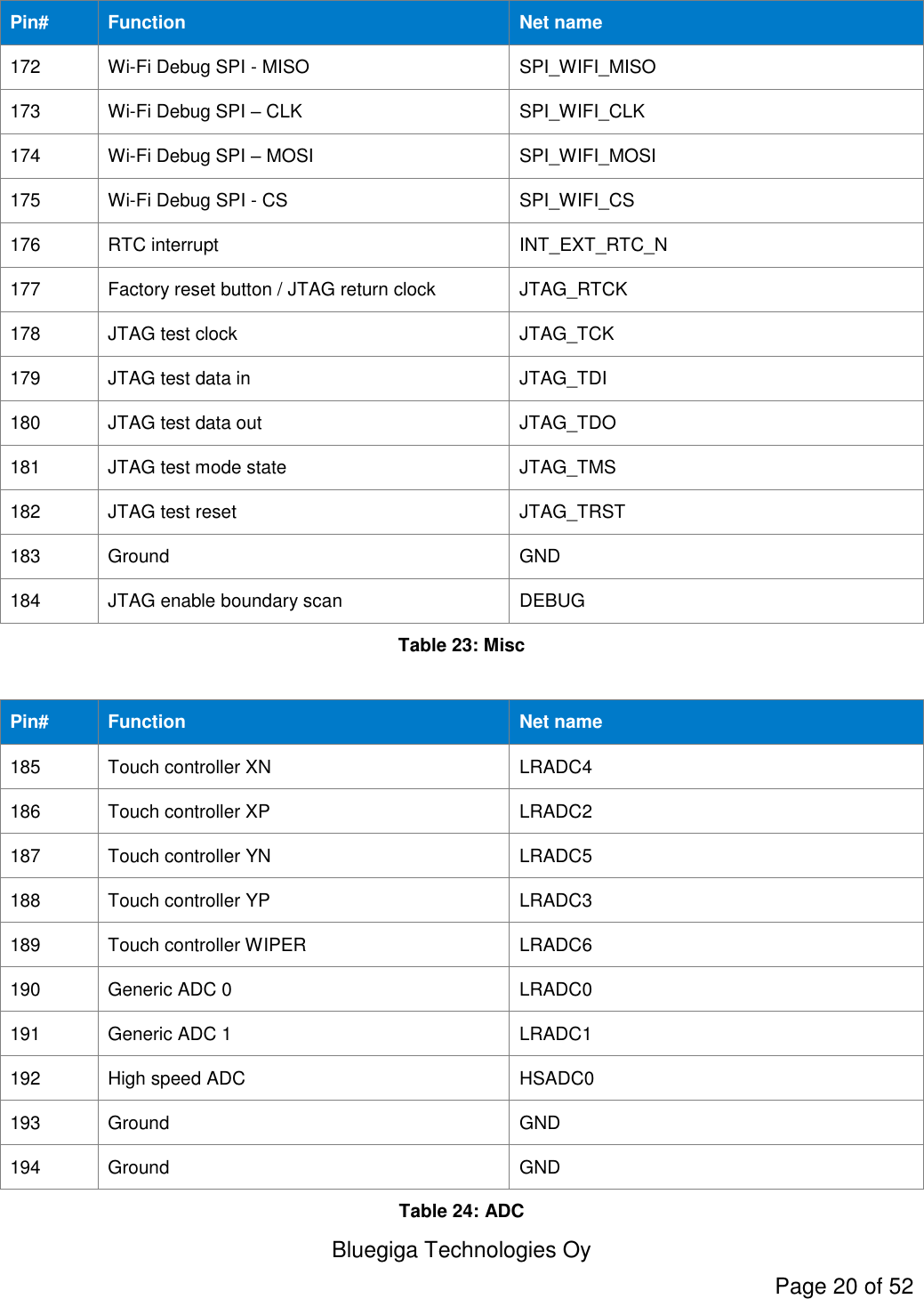
![Bluegiga Technologies Oy Page 24 of 52 4 Processor subsystem The processor belongs to the Freescale i.MX28-family and integrates an ARM9 core operating at 454MHz. The standard APX4 variant uses the i.MX283 processor. The module also has 128MB of SLC NAND flash and 64MB of DDR2-400 memory. For more details regarding the features the processor offers, please see the Freescale Reference Manual. By default the module boots from the NAND flash into the U-Boot boot loader environment. From there the boot loader loads a Linux kernel which boots into the Bluegiga Linux userspace. 4.1 Bootmodes The module supports booting from multiple different media including NAND Flash, Secure Digital (SD) cards, MMC cards, I2C EEPROM and USB (in a device mode). The selected boot media can be selected using the LCD_DATA[0-3] signals or in the case of USB recovery boot, by tying the BOOTMODE pin to ground. By default the module boots from internal NAND flash, meaning that LCD_DATA[3], LCD_DATA[1] and LCD_DATA[0] have pull-downs on the module and LCD_DATA[2] has a pull-up. Default boot mode in bold face. The module has pull-ups and pull-downs so that when LCD_DATA[0]..LCD_DATA[3] are left unconnected the module boots from internal NAND. After boot the LCD_DATA lines can be used fro any purpose. LCD_DATA[3] LCD_DATA[2] LCD_DATA[1] LCD_DATA[0] Port 0 0 0 0 USB0 device mode boot 0 0 0 1 EEPROM connected to I2C0 0 0 1 0 SPI flash on SSP2 (non-Wi-Fi version only) 0 0 1 1 SPI flash on SSP3 (not available on standard versions) 0 1 0 0 Module’s internal NAND Flash 0 1 1 0 Wait for JTAG connection 1 0 0 0 SPI EEPROM on SSP3 (not available on standard versions) 1 0 0 1 SD/MMC card on SSP0 1 0 1 0 SD/MMC on SSP1 (not available on standard versions) Table 27: Bootmodes](https://usermanual.wiki/Silicon-Laboratories-Finland/APX4/User-Guide-2023175-Page-24.png)