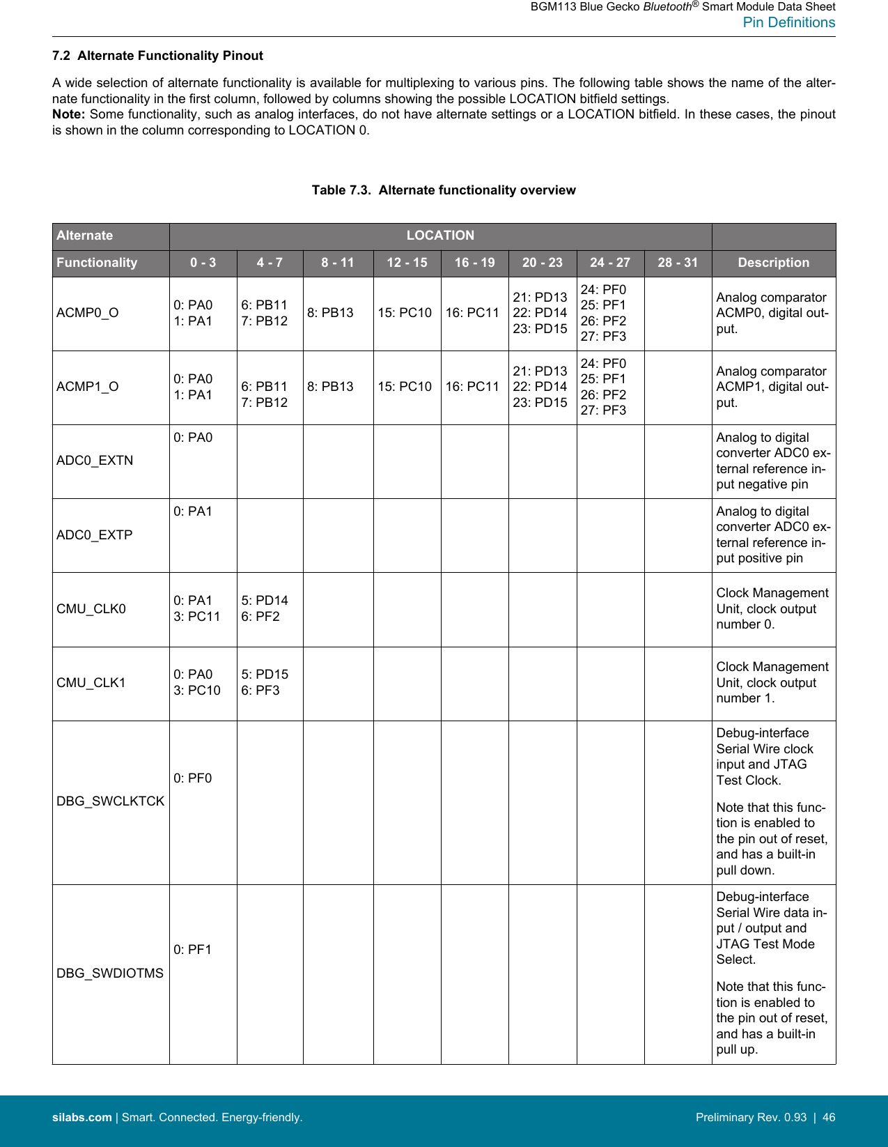
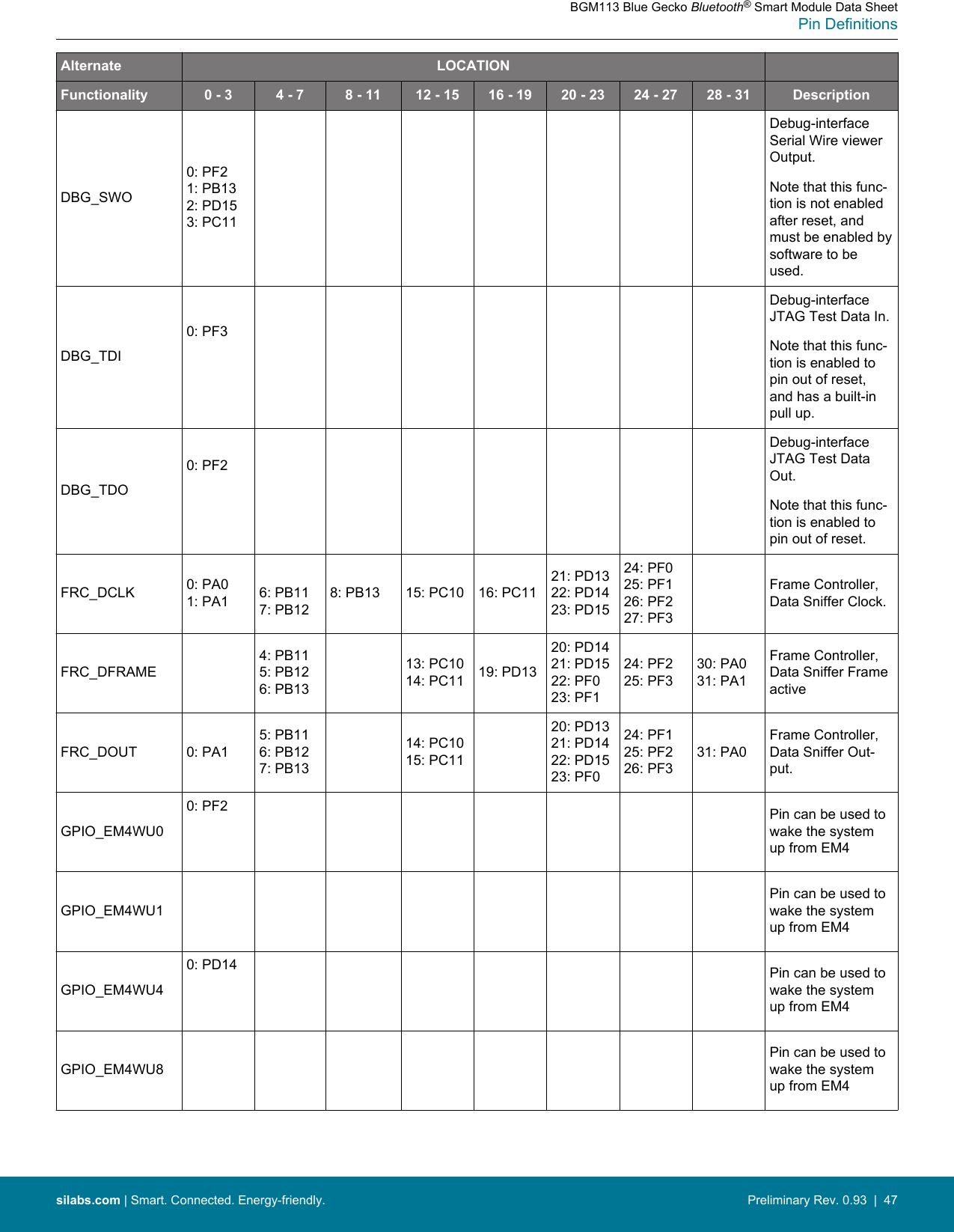
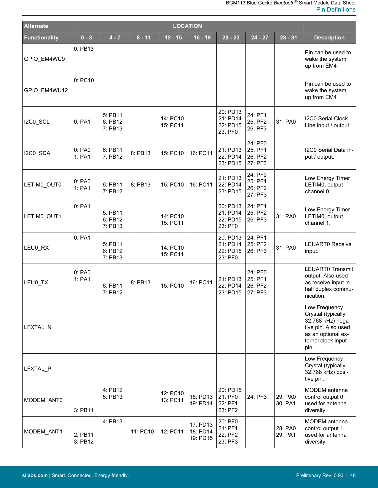
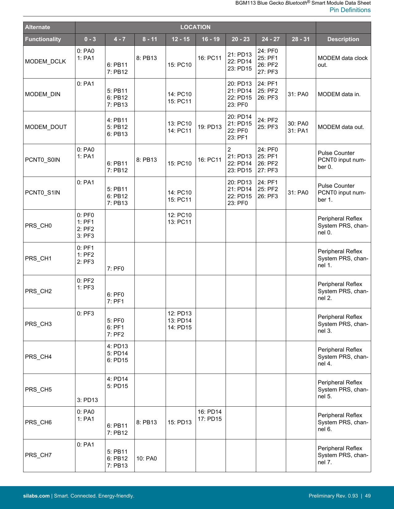
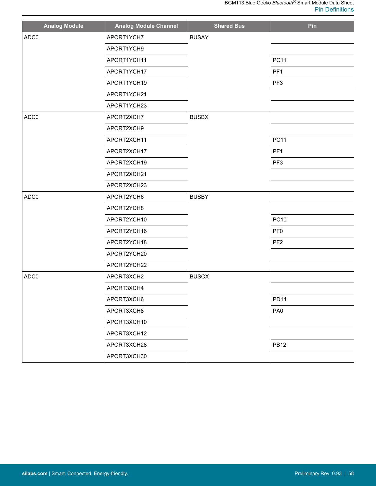
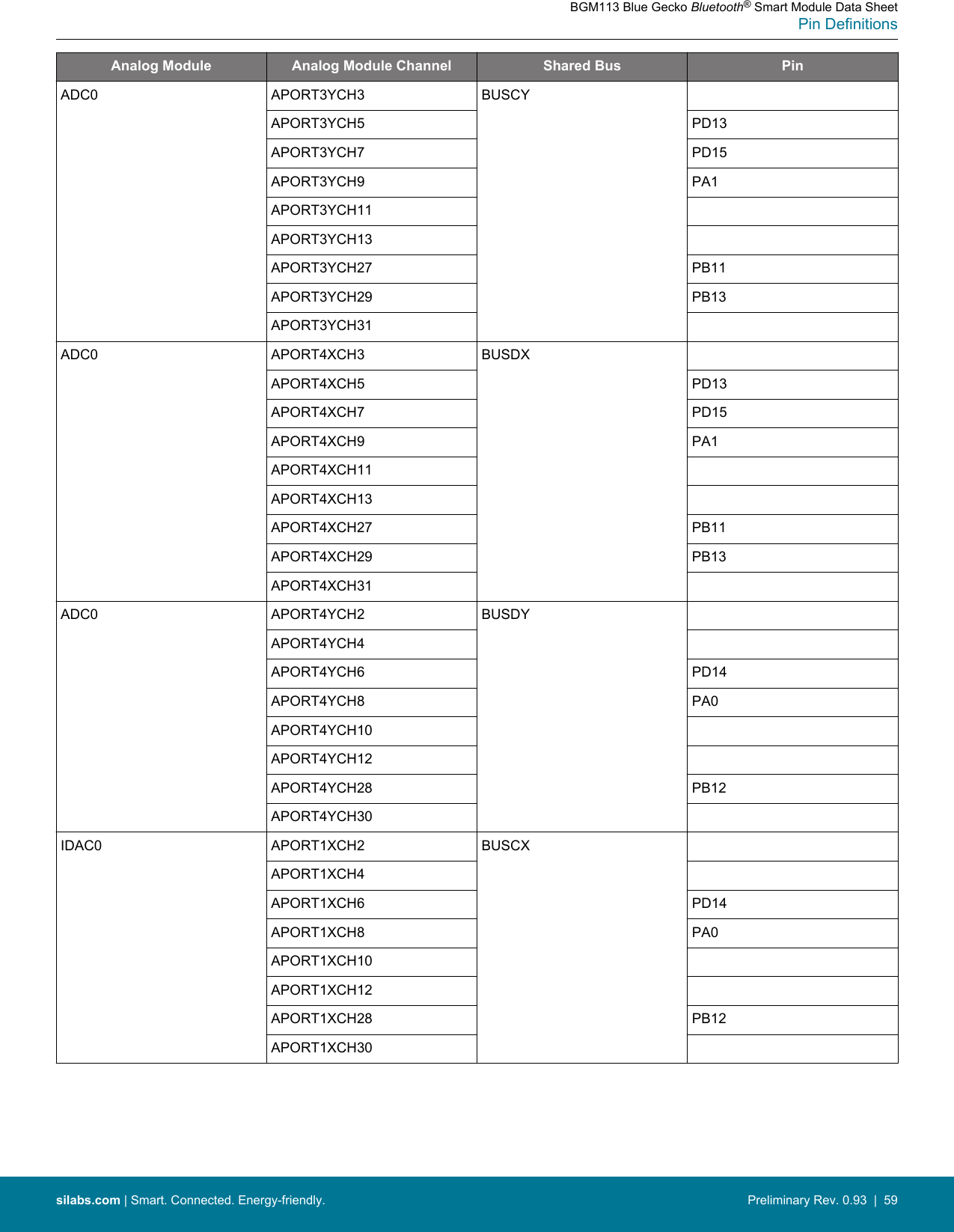
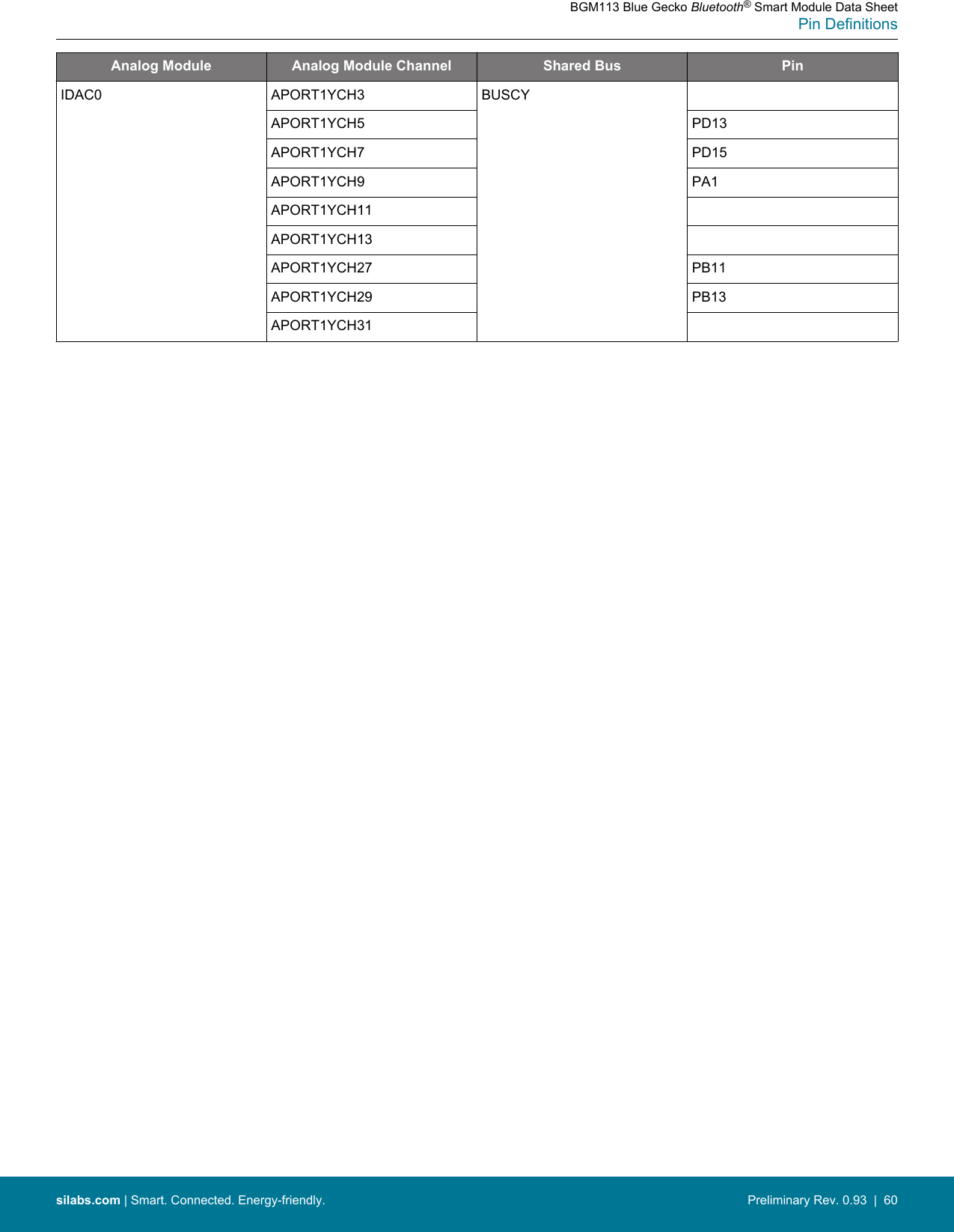
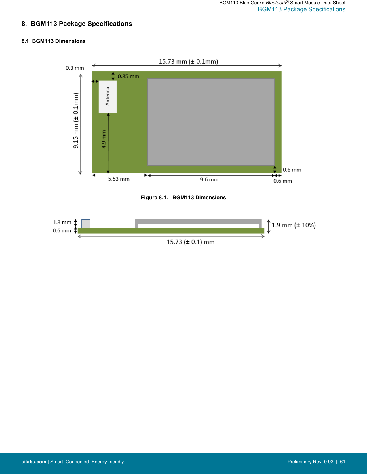
Silicon Laboratories Finland BGM113 Blue Gecko BGM113 Bluetooth Smart Module User Manual Users manual
Silicon Laboratories Finland Oy Blue Gecko BGM113 Bluetooth Smart Module Users manual
UserManual.wiki
>
Silicon Laboratories Finland
>
BGM113 User Manual
Users manual
Navigation menu
Upload a User Manual
Namespaces
Wiki Guide
HTML
PDF
Info
Views
User Manual
Discussion / Help
Navigation
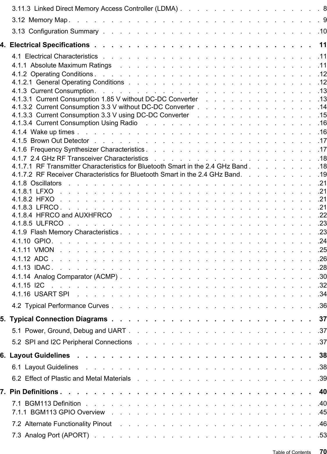
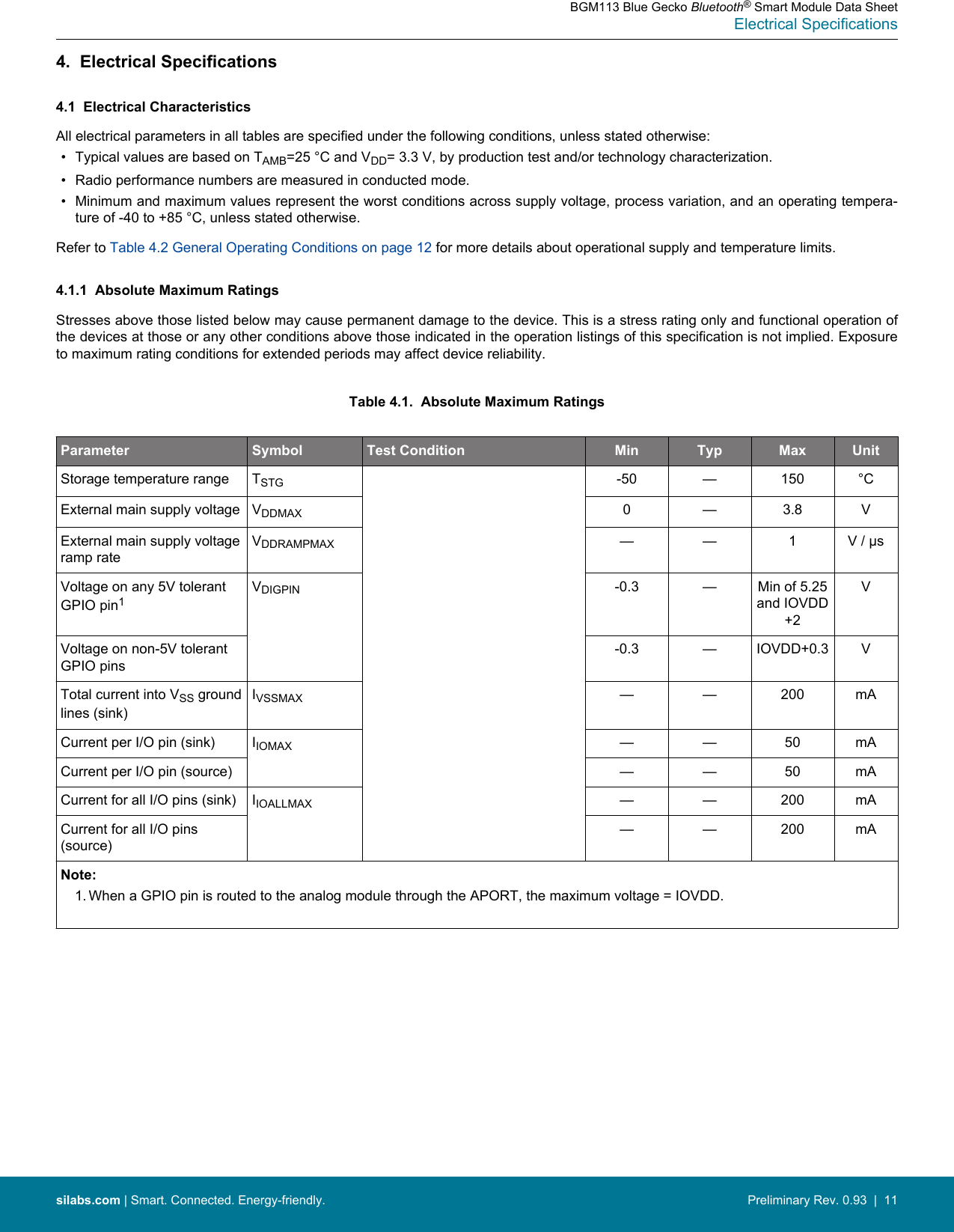
![Figure 3.3. BGM113 Memory Map — Peripherals3.13 Configuration SummaryThe features of the BGM113 are a subset of the feature set described in the device reference manual. The table below describes de-vice specific implementation of the features. Remaining modules support full configuration.Table 3.2. Configuration SummaryModule Configuration Pin ConnectionsUSART0 IrDA SmartCard US0_TX, US0_RX, US0_CLK, US0_CSUSART1 IrDA I2S SmartCard US1_TX, US1_RX, US1_CLK, US1_CSTIMER0 with DTI TIM0_CC[2:0], TIM0_CDTI[2:0]TIMER1 TIM1_CC[3:0]BGM113 Blue Gecko Bluetooth® Smart Module Data SheetSystem Overviewsilabs.com | Smart. Connected. Energy-friendly. Preliminary Rev. 0.93 | 10](https://usermanual.wiki/Silicon-Laboratories-Finland/BGM113/User-Guide-3018453-Page-11.png)
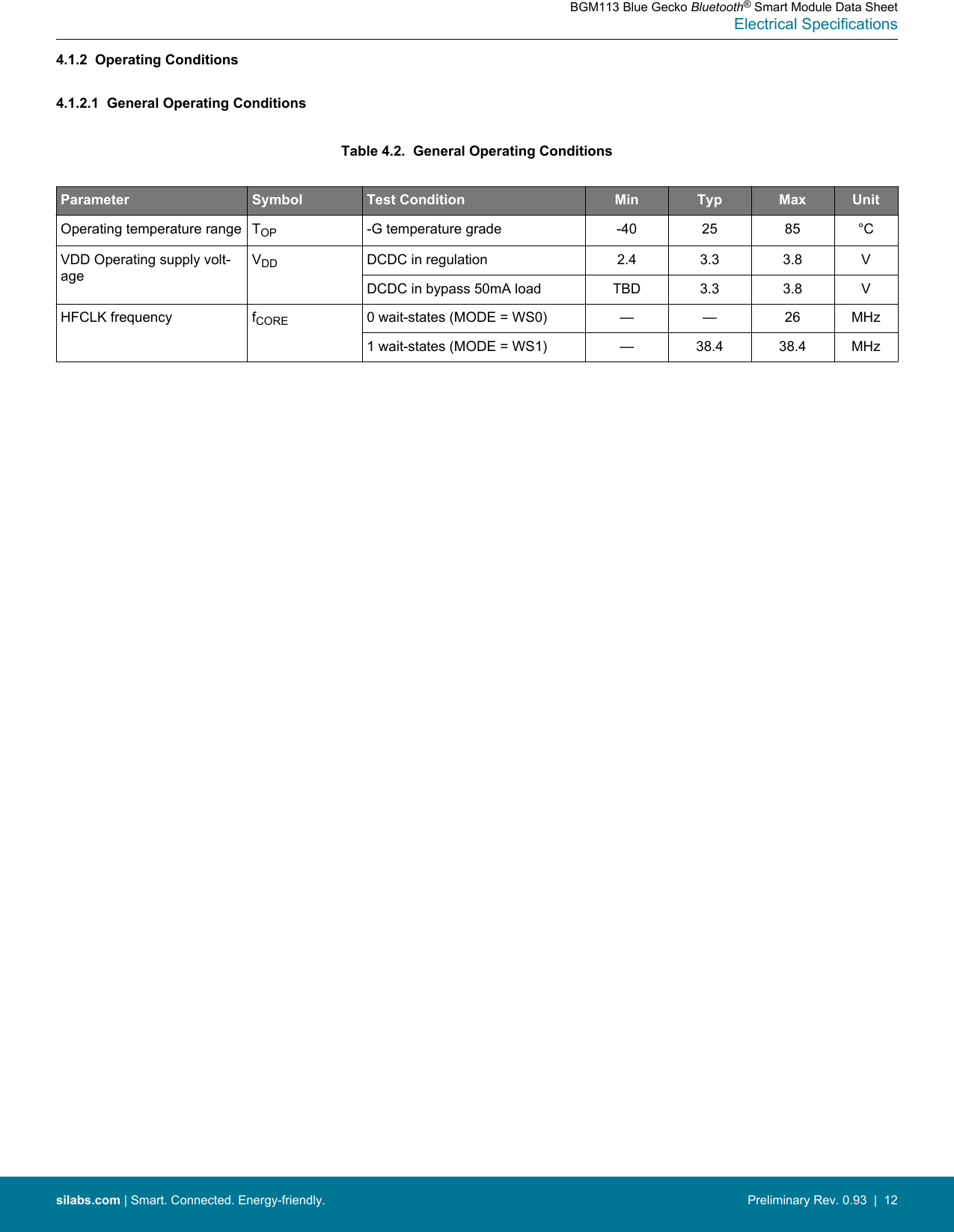
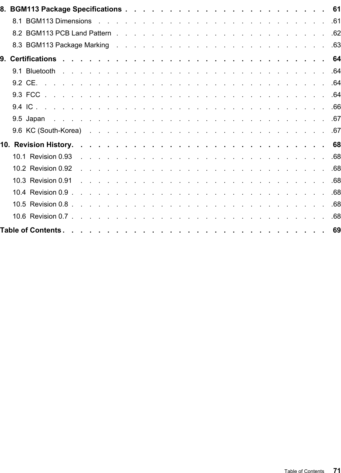
![4.1.7 2.4 GHz RF Transceiver Characteristics4.1.7.1 RF Transmitter Characteristics for Bluetooth Smart in the 2.4 GHz BandTable 4.10. RF Transmitter Characteristics for Bluetooth Smart in the 2.4GHz BandParameter Symbol Test Condition Min Typ Max UnitTransmit 6dB bandwidth TXBW — 740 — kHzPower spectral density limit PSDLIMIT Per FCC part 15.247 — -6.5 — dBm/3kHzPer ETSI 300.328 at 10 dBm/1MHz— 10 — dBmOccupied channel bandwidthper ETSI EN300.328OCPETSI328 99% BW at highest and lowestchannels in band— 1.1 — MHzIn-band spurious emissions,with allowed exceptions1SPURINB At ±2 MHz — -39.8 — dBmAt ±3 MHz — -42.1 — dBmEmissions of harmonics out-of-band, per FCC part15.247SPURHRM_FCC 2nd,3rd, 5, 6, 8, 9,10 harmonics;continuous transmission of modu-lated carrier— -47.3 — dBmSpurious emissions out-of-band, per FCC part 15.247,excluding harmonics cap-tured in SPURHARM,FCC. Re-stricted BandsSPUROOB_FCC Above 2.483 GHz or below 2.4GHz; continuous transmission ofmodulated carrier2— -47 — dBmSpurious emissions out-of-band, per FCC part 15.247,excluding harmonics cap-tured in SPURHARM,FCC.Non Restricted BandsAbove 2.483 GHz or below 2.4GHz; continuous transmission ofmodulated carrier— -26 — dBcSpurious emissions out-of-band; per ETSI 300.328SPURETSI328 [2400-BW to 2400] MHz, [2483.5to 2483.5+BW] MHz— -16 — dBm[2400-2BW to 2400-BW] MHz,[2483.5+BW to 2483.5+2BW]MHz per ETSI 300.328— -26 — dBmSpurious emissions per ETSIEN300.440SPURETSI440 47-74 MHz,87.5-108 MHz,174-230 MHz, 470-862 MHz— -60 — dBm25-1000 MHz — -42 — dBm1-12 GHz — -36 — dBmNote:1. Per Bluetooth Core_4.2, Section 3.2.2, exceptions are allowed in up to three bands of 1 MHz width, centered on a frequencywhich is an integer multiple of 1 MHz. These exceptions shall have an absolute value of -20 dBm or less.2. For 2480 Mhz, a maximum duty cycle of 20% is used to achieve this value. BGM113 Blue Gecko Bluetooth® Smart Module Data SheetElectrical Specificationssilabs.com | Smart. Connected. Energy-friendly. Preliminary Rev. 0.93 | 18](https://usermanual.wiki/Silicon-Laboratories-Finland/BGM113/User-Guide-3018453-Page-19.png)
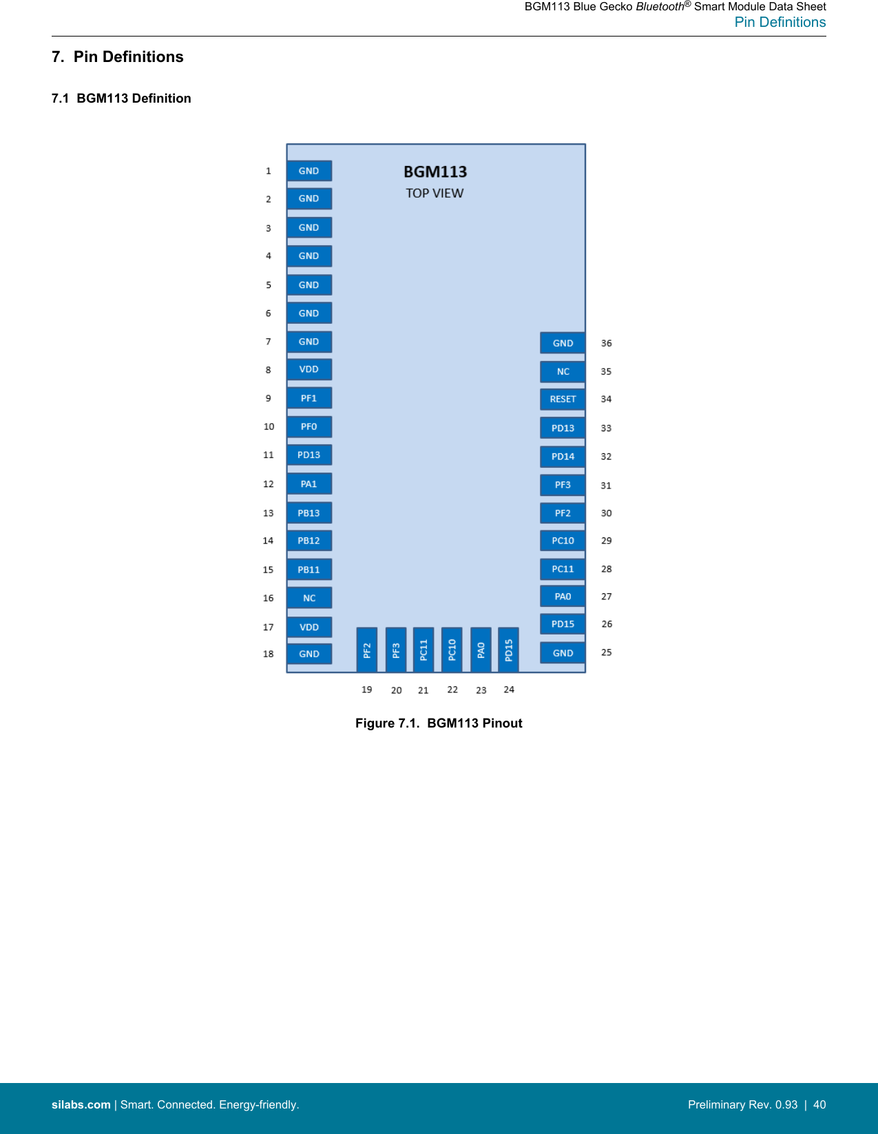
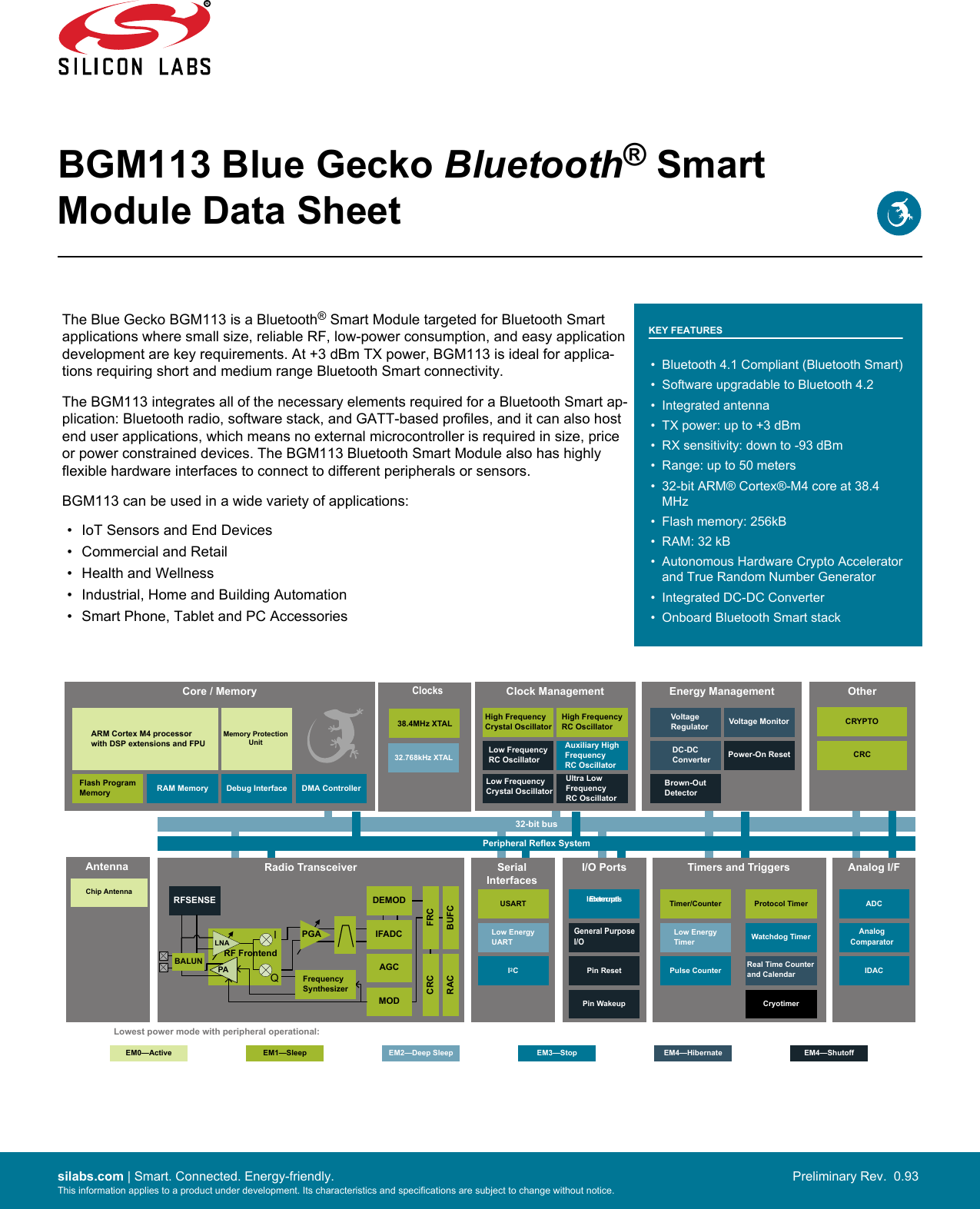
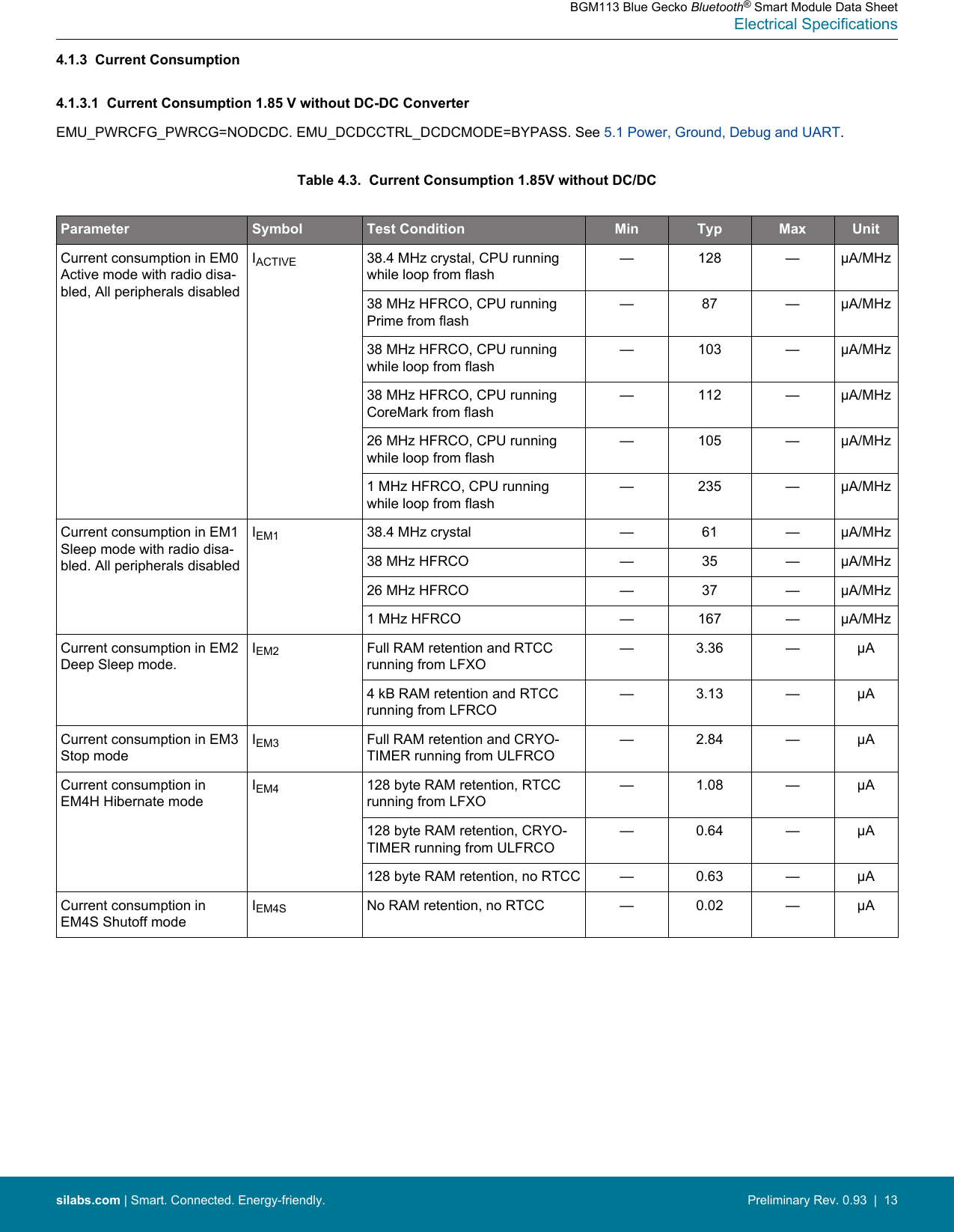
![Table 7.1. Device PinoutPin# and Name Pin Alternate Functionality / DescriptionPin#Pin Name Analog Timers Communication Radio Other1-7,18,25,36GND Ground10 PF0BUSAX [ADC0:APORT1XCH16ACMP0:APORT1XCH16ACMP1:APORT1XCH16]BUSBY [ADC0:APORT2YCH16ACMP0:APORT2YCH16ACMP1:APORT2YCH16]TIM0_CC0 #24TIM0_CC1 #23TIM0_CC2 #22TIM0_CDTI0 #21TIM0_CDTI1 #20TIM0_CDTI2 #19TIM1_CC0 #24TIM1_CC1 #23TIM1_CC2 #22TIM1_CC3 #21 LE-TIM0_OUT0 #24LETIM0_OUT1 #23PCNT0_S0IN #24PCNT0_S1IN #23US0_TX #24US0_RX #23US0_CLK #22US0_CS #21US0_CTS #20US0_RTS #19US1_TX #24US1_RX #23US1_CLK #22US1_CS #21US1_CTS #20US1_RTS #19LEU0_TX #24LEU0_RX #23I2C0_SDA #24I2C0_SCL #23FRC_DCLK #24FRC_DOUT #23FRC_DFRAME #22MODEM_DCLK #24MODEM_DIN #23MODEM_DOUT #22MODEM_ANT0 #21MODEM_ANT1 #20PRS_CH0 #0PRS_CH1 #7PRS_CH2 #6PRS_CH3 #5ACMP0_O #24ACMP1_O #24DBG_SWCLKTCK#09 PF1BUSAY [ADC0:APORT1YCH17ACMP0:APORT1YCH17ACMP1:APORT1YCH17]BUSBX [ADC0:APORT2XCH17ACMP0:APORT2XCH17ACMP1:APORT2XCH17]TIM0_CC0 #25TIM0_CC1 #24TIM0_CC2 #23TIM0_CDTI0 #22TIM0_CDTI1 #21TIM0_CDTI2 #20TIM1_CC0 #25TIM1_CC1 #24TIM1_CC2 #23TIM1_CC3 #22 LE-TIM0_OUT0 #25LETIM0_OUT1 #24PCNT0_S0IN #25PCNT0_S1IN #24US0_TX #25US0_RX #24US0_CLK #23US0_CS #22US0_CTS #21US0_RTS #20US1_TX #25US1_RX #24US1_CLK #23US1_CS #22US1_CTS #21US1_RTS #20LEU0_TX #25LEU0_RX #24I2C0_SDA #25I2C0_SCL #24FRC_DCLK #25FRC_DOUT #24FRC_DFRAME #23MODEM_DCLK #25MODEM_DIN #24MODEM_DOUT #23MODEM_ANT0 #22MODEM_ANT1 #21PRS_CH0 #1PRS_CH1 #0PRS_CH2 #7PRS_CH3 #6ACMP0_O #25ACMP1_O #25DBG_SWDIOTMS#019,30 PF2BUSAX [ADC0:APORT1XCH18ACMP0:APORT1XCH18ACMP1:APORT1XCH18]BUSBY [ADC0:APORT2YCH18ACMP0:APORT2YCH18ACMP1:APORT2YCH18]TIM0_CC0 #26TIM0_CC1 #25TIM0_CC2 #24TIM0_CDTI0 #23TIM0_CDTI1 #22TIM0_CDTI2 #21TIM1_CC0 #26TIM1_CC1 #25TIM1_CC2 #24TIM1_CC3 #23 LE-TIM0_OUT0 #26LETIM0_OUT1 #25PCNT0_S0IN #26PCNT0_S1IN #25US0_TX #26US0_RX #25US0_CLK #24US0_CS #23US0_CTS #22US0_RTS #21US1_TX #26US1_RX #25US1_CLK #24US1_CS #23US1_CTS #22US1_RTS #21LEU0_TX #26LEU0_RX #25I2C0_SDA #26I2C0_SCL #25FRC_DCLK #26FRC_DOUT #25FRC_DFRAME #24MODEM_DCLK #26MODEM_DIN #25MODEM_DOUT #24MODEM_ANT0 #23MODEM_ANT1 #22CMU_CLK0 #6PRS_CH0 #2PRS_CH1 #1PRS_CH2 #0PRS_CH3 #7ACMP0_O #26ACMP1_O #26DBG_TDO #0DBG_SWO #0GPIO_EM4WU0BGM113 Blue Gecko Bluetooth® Smart Module Data SheetPin Definitionssilabs.com | Smart. Connected. Energy-friendly. Preliminary Rev. 0.93 | 41](https://usermanual.wiki/Silicon-Laboratories-Finland/BGM113/User-Guide-3018453-Page-42.png)
![Pin# and Name Pin Alternate Functionality / DescriptionPin#Pin Name Analog Timers Communication Radio Other20,31 PF3BUSAY [ADC0:APORT1YCH19ACMP0:APORT1YCH19ACMP1:APORT1YCH19]BUSBX [ADC0:APORT2XCH19ACMP0:APORT2XCH19ACMP1:APORT2XCH19]TIM0_CC0 #27TIM0_CC1 #26TIM0_CC2 #25TIM0_CDTI0 #24TIM0_CDTI1 #23TIM0_CDTI2 #22TIM1_CC0 #27TIM1_CC1 #26TIM1_CC2 #25TIM1_CC3 #24 LE-TIM0_OUT0 #27LETIM0_OUT1 #26PCNT0_S0IN #27PCNT0_S1IN #26US0_TX #27US0_RX #26US0_CLK #25US0_CS #24US0_CTS #23US0_RTS #22US1_TX #27US1_RX #26US1_CLK #25US1_CS #24US1_CTS #23US1_RTS #22LEU0_TX #27LEU0_RX #26I2C0_SDA #27I2C0_SCL #26FRC_DCLK #27FRC_DOUT #26FRC_DFRAME #25MODEM_DCLK #27MODEM_DIN #26MODEM_DOUT #25MODEM_ANT0 #24MODEM_ANT1 #23CMU_CLK1 #6PRS_CH0 #3PRS_CH1 #2PRS_CH2 #1PRS_CH3 #0ACMP0_O #27ACMP1_O #27DBG_TDI #08,17 VDD Radio power supply34 RESETn Reset input, active low.To apply an external reset source to this pin, it is required to only drive this pin lowduring reset, and let the internal pull-up ensure that reset is released.11,33 PD13BUSCY [ADC0:APORT3YCH5ACMP0:APORT3YCH5ACMP1:APORT3YCH5IDAC0:APORT1YCH5]BUSDX [ADC0:APORT4XCH5ACMP0:APORT4XCH5ACMP1:APORT4XCH5]TIM0_CC0 #21TIM0_CC1 #20TIM0_CC2 #19TIM0_CDTI0 #18TIM0_CDTI1 #17TIM0_CDTI2 #16TIM1_CC0 #21TIM1_CC1 #20TIM1_CC2 #19TIM1_CC3 #18 LE-TIM0_OUT0 #21LETIM0_OUT1 #20PCNT0_S0IN #21PCNT0_S1IN #20US0_TX #21US0_RX #20US0_CLK #19US0_CS #18US0_CTS #17US0_RTS #16US1_TX #21US1_RX #20US1_CLK #19US1_CS #18US1_CTS #17US1_RTS #16LEU0_TX #21LEU0_RX #20I2C0_SDA #21I2C0_SCL #20FRC_DCLK #21FRC_DOUT #20FRC_DFRAME #19MODEM_DCLK #21MODEM_DIN #20MODEM_DOUT #19MODEM_ANT0 #18MODEM_ANT1 #17PRS_CH3 #12PRS_CH4 #4PRS_CH5 #3PRS_CH6 #15ACMP0_O #21ACMP1_O #2132 PD14BUSCX [ADC0:APORT3XCH6ACMP0:APORT3XCH6ACMP1:APORT3XCH6IDAC0:APORT1XCH6]BUSDY [ADC0:APORT4YCH6ACMP0:APORT4YCH6ACMP1:APORT4YCH6]TIM0_CC0 #22TIM0_CC1 #21TIM0_CC2 #20TIM0_CDTI0 #19TIM0_CDTI1 #18TIM0_CDTI2 #17TIM1_CC0 #22TIM1_CC1 #21TIM1_CC2 #20TIM1_CC3 #19 LE-TIM0_OUT0 #22LETIM0_OUT1 #21PCNT0_S0IN #22PCNT0_S1IN #21US0_TX #22US0_RX #21US0_CLK #20US0_CS #19US0_CTS #18US0_RTS #17US1_TX #22US1_RX #21US1_CLK #20US1_CS #19US1_CTS #18US1_RTS #17LEU0_TX #22LEU0_RX #21I2C0_SDA #22I2C0_SCL #21FRC_DCLK #22FRC_DOUT #21FRC_DFRAME #20MODEM_DCLK #22MODEM_DIN #21MODEM_DOUT #20MODEM_ANT0 #19MODEM_ANT1 #18CMU_CLK0 #5PRS_CH3 #13PRS_CH4 #5PRS_CH5 #4PRS_CH6 #16ACMP0_O #22ACMP1_O #22GPIO_EM4WU4BGM113 Blue Gecko Bluetooth® Smart Module Data SheetPin Definitionssilabs.com | Smart. Connected. Energy-friendly. Preliminary Rev. 0.93 | 42](https://usermanual.wiki/Silicon-Laboratories-Finland/BGM113/User-Guide-3018453-Page-43.png)
![Pin# and Name Pin Alternate Functionality / DescriptionPin#Pin Name Analog Timers Communication Radio Other24,26 PD15BUSCY [ADC0:APORT3YCH7ACMP0:APORT3YCH7ACMP1:APORT3YCH7IDAC0:APORT1YCH7]BUSDX [ADC0:APORT4XCH7ACMP0:APORT4XCH7ACMP1:APORT4XCH7]TIM0_CC0 #23TIM0_CC1 #22TIM0_CC2 #21TIM0_CDTI0 #20TIM0_CDTI1 #19TIM0_CDTI2 #18TIM1_CC0 #23TIM1_CC1 #22TIM1_CC2 #21TIM1_CC3 #20 LE-TIM0_OUT0 #23LETIM0_OUT1 #22PCNT0_S0IN #23PCNT0_S1IN #22US0_TX #23US0_RX #22US0_CLK #21US0_CS #20US0_CTS #19US0_RTS #18US1_TX #23US1_RX #22US1_CLK #21US1_CS #20US1_CTS #19US1_RTS #18LEU0_TX #23LEU0_RX #22I2C0_SDA #23I2C0_SCL #22FRC_DCLK #23FRC_DOUT #22FRC_DFRAME #21MODEM_DCLK #23MODEM_DIN #22MODEM_DOUT #21MODEM_ANT0 #20MODEM_ANT1 #19CMU_CLK1 #5PRS_CH3 #14PRS_CH4 #6PRS_CH5 #5PRS_CH6 #17ACMP0_O #23ACMP1_O #23DBG_SWO #223,27 PA0ADC0_EXTNBUSCX [ADC0:APORT3XCH8ACMP0:APORT3XCH8ACMP1:APORT3XCH8IDAC0:APORT1XCH8]BUSDY [ADC0:APORT4YCH8ACMP0:APORT4YCH8ACMP1:APORT4YCH8]TIM0_CC0 #0TIM0_CC1 #31TIM0_CC2 #30TIM0_CDTI0 #29TIM0_CDTI1 #28TIM0_CDTI2 #27TIM1_CC0 #0TIM1_CC1 #31TIM1_CC2 #30TIM1_CC3 #29 LE-TIM0_OUT0 #0 LE-TIM0_OUT1 #31PCNT0_S0IN #0PCNT0_S1IN #31US0_TX #0US0_RX #31US0_CLK #30US0_CS #29US0_CTS #28US0_RTS #27US1_TX #0US1_RX #31US1_CLK #30US1_CS #29US1_CTS #28US1_RTS #27LEU0_TX #0LEU0_RX #31I2C0_SDA #0I2C0_SCL #31FRC_DCLK #0FRC_DOUT #31FRC_DFRAME #30MODEM_DCLK #0MODEM_DIN #31MODEM_DOUT #30MODEM_ANT0 #29MODEM_ANT1 #28CMU_CLK1 #0PRS_CH6 #0PRS_CH7 #10PRS_CH8 #9PRS_CH9 #8ACMP0_O #0ACMP1_O #012 PA1ADC0_EXTPBUSCY [ADC0:APORT3YCH9ACMP0:APORT3YCH9ACMP1:APORT3YCH9IDAC0:APORT1YCH9]BUSDX [ADC0:APORT4XCH9ACMP0:APORT4XCH9ACMP1:APORT4XCH9]TIM0_CC0 #1TIM0_CC1 #0TIM0_CC2 #31TIM0_CDTI0 #30TIM0_CDTI1 #29TIM0_CDTI2 #28TIM1_CC0 #1TIM1_CC1 #0TIM1_CC2 #31TIM1_CC3 #30 LE-TIM0_OUT0 #1 LE-TIM0_OUT1 #0PCNT0_S0IN #1PCNT0_S1IN #0US0_TX #1US0_RX #0US0_CLK #31US0_CS #30US0_CTS #29US0_RTS #28US1_TX #1US1_RX #0US1_CLK #31US1_CS #30US1_CTS #29US1_RTS #28LEU0_TX #1LEU0_RX #0I2C0_SDA #1I2C0_SCL #0FRC_DCLK #1FRC_DOUT #0FRC_DFRAME #31MODEM_DCLK #1MODEM_DIN #0MODEM_DOUT #31MODEM_ANT0 #30MODEM_ANT1 #29CMU_CLK0 #0PRS_CH6 #1PRS_CH7 #0PRS_CH8 #10PRS_CH9 #9ACMP0_O #1ACMP1_O #1BGM113 Blue Gecko Bluetooth® Smart Module Data SheetPin Definitionssilabs.com | Smart. Connected. Energy-friendly. Preliminary Rev. 0.93 | 43](https://usermanual.wiki/Silicon-Laboratories-Finland/BGM113/User-Guide-3018453-Page-44.png)
![Pin# and Name Pin Alternate Functionality / DescriptionPin#Pin Name Analog Timers Communication Radio Other15 PB11BUSCY [ADC0:APORT3YCH27ACMP0:APORT3YCH27ACMP1:APORT3YCH27IDAC0:APORT1YCH27]BUSDX [ADC0:APORT4XCH27ACMP0:APORT4XCH27ACMP1:APORT4XCH27]TIM0_CC0 #6TIM0_CC1 #5TIM0_CC2 #4TIM0_CDTI0 #3TIM0_CDTI1 #2TIM0_CDTI2 #1TIM1_CC0 #6TIM1_CC1 #5TIM1_CC2 #4TIM1_CC3 #3 LE-TIM0_OUT0 #6 LE-TIM0_OUT1 #5PCNT0_S0IN #6PCNT0_S1IN #5US0_TX #6US0_RX #5US0_CLK #4US0_CS #3US0_CTS #2US0_RTS #1US1_TX #6US1_RX #5US1_CLK #4US1_CS #3US1_CTS #2US1_RTS #1LEU0_TX #6LEU0_RX #5I2C0_SDA #6I2C0_SCL #5FRC_DCLK #6FRC_DOUT #5FRC_DFRAME #4MODEM_DCLK #6MODEM_DIN #5MODEM_DOUT #4MODEM_ANT0 #3MODEM_ANT1 #2PRS_CH6 #6PRS_CH7 #5PRS_CH8 #4PRS_CH9 #3ACMP0_O #6ACMP1_O #614 PB12BUSCX [ADC0:APORT3XCH28ACMP0:APORT3XCH28ACMP1:APORT3XCH28IDAC0:APORT1XCH28]BUSDY [ADC0:APORT4YCH28ACMP0:APORT4YCH28ACMP1:APORT4YCH28]TIM0_CC0 #7TIM0_CC1 #6TIM0_CC2 #5TIM0_CDTI0 #4TIM0_CDTI1 #3TIM0_CDTI2 #2TIM1_CC0 #7TIM1_CC1 #6TIM1_CC2 #5TIM1_CC3 #4 LE-TIM0_OUT0 #7 LE-TIM0_OUT1 #6PCNT0_S0IN #7PCNT0_S1IN #6US0_TX #7US0_RX #6US0_CLK #5US0_CS #4US0_CTS #3US0_RTS #2US1_TX #7US1_RX #6US1_CLK #5US1_CS #4US1_CTS #3US1_RTS #2LEU0_TX #7LEU0_RX #6I2C0_SDA #7I2C0_SCL #6FRC_DCLK #7FRC_DOUT #6FRC_DFRAME #5MODEM_DCLK #7MODEM_DIN #6MODEM_DOUT #5MODEM_ANT0 #4MODEM_ANT1 #3PRS_CH6 #7PRS_CH7 #6PRS_CH8 #5PRS_CH9 #4ACMP0_O #7ACMP1_O #713 PB13BUSCY [ADC0:APORT3YCH29ACMP0:APORT3YCH29ACMP1:APORT3YCH29IDAC0:APORT1YCH29]BUSDX [ADC0:APORT4XCH29ACMP0:APORT4XCH29ACMP1:APORT4XCH29]TIM0_CC0 #8TIM0_CC1 #7TIM0_CC2 #6TIM0_CDTI0 #5TIM0_CDTI1 #4TIM0_CDTI2 #3TIM1_CC0 #8TIM1_CC1 #7TIM1_CC2 #6TIM1_CC3 #5 LE-TIM0_OUT0 #8 LE-TIM0_OUT1 #7PCNT0_S0IN #8PCNT0_S1IN #7US0_TX #8US0_RX #7US0_CLK #6US0_CS #5US0_CTS #4US0_RTS #3US1_TX #8US1_RX #7US1_CLK #6US1_CS #5US1_CTS #4US1_RTS #3LEU0_TX #8LEU0_RX #7I2C0_SDA #8I2C0_SCL #7FRC_DCLK #8FRC_DOUT #7FRC_DFRAME #6MODEM_DCLK #8MODEM_DIN #7MODEM_DOUT #6MODEM_ANT0 #5MODEM_ANT1 #4PRS_CH6 #8PRS_CH7 #7PRS_CH8 #6PRS_CH9 #5ACMP0_O #8ACMP1_O #8DBG_SWO #1GPIO_EM4WU9BGM113 Blue Gecko Bluetooth® Smart Module Data SheetPin Definitionssilabs.com | Smart. Connected. Energy-friendly. Preliminary Rev. 0.93 | 44](https://usermanual.wiki/Silicon-Laboratories-Finland/BGM113/User-Guide-3018453-Page-45.png)
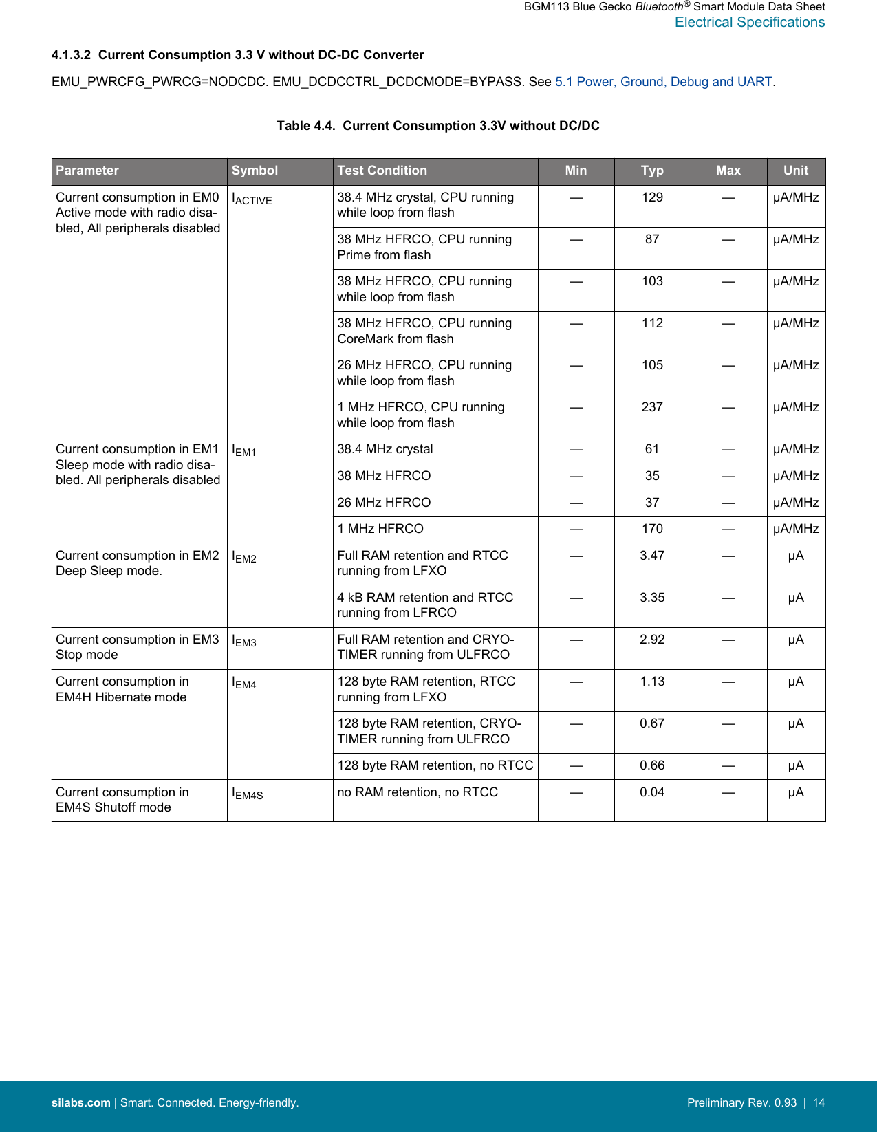
![Pin# and Name Pin Alternate Functionality / DescriptionPin#Pin Name Analog Timers Communication Radio Other22,29 PC10BUSAX [ADC0:APORT1XCH10ACMP0:APORT1XCH10ACMP1:APORT1XCH10]BUSBY [ADC0:APORT2YCH10ACMP0:APORT2YCH10ACMP1:APORT2YCH10]TIM0_CC0 #15TIM0_CC1 #14TIM0_CC2 #13TIM0_CDTI0 #12TIM0_CDTI1 #11TIM0_CDTI2 #10TIM1_CC0 #15TIM1_CC1 #14TIM1_CC2 #13TIM1_CC3 #12 LE-TIM0_OUT0 #15LETIM0_OUT1 #14PCNT0_S0IN #15PCNT0_S1IN #14US0_TX #15US0_RX #14US0_CLK #13US0_CS #12US0_CTS #11US0_RTS #10US1_TX #15US1_RX #14US1_CLK #13US1_CS #12US1_CTS #11US1_RTS #10LEU0_TX #15LEU0_RX #14I2C0_SDA #15I2C0_SCL #14FRC_DCLK #15FRC_DOUT #14FRC_DFRAME #13MODEM_DCLK #15MODEM_DIN #14MODEM_DOUT #13MODEM_ANT0 #12MODEM_ANT1 #11CMU_CLK1 #3PRS_CH0 #12PRS_CH9 #15PRS_CH10 #4PRS_CH11 #3ACMP0_O #15ACMP1_O #15GPIO_EM4WU1221,28 PC11BUSAY [ADC0:APORT1YCH11ACMP0:APORT1YCH11ACMP1:APORT1YCH11]BUSBX [ADC0:APORT2XCH11ACMP0:APORT2XCH11ACMP1:APORT2XCH11]TIM0_CC0 #16TIM0_CC1 #15TIM0_CC2 #14TIM0_CDTI0 #13TIM0_CDTI1 #12TIM0_CDTI2 #11TIM1_CC0 #16TIM1_CC1 #15TIM1_CC2 #14TIM1_CC3 #13 LE-TIM0_OUT0 #16LETIM0_OUT1 #15PCNT0_S0IN #16PCNT0_S1IN #15US0_TX #16US0_RX #15US0_CLK #14US0_CS #13US0_CTS #12US0_RTS #11US1_TX #16US1_RX #15US1_CLK #14US1_CS #13US1_CTS #12US1_RTS #11LEU0_TX #16LEU0_RX #15I2C0_SDA #16I2C0_SCL #15FRC_DCLK #16FRC_DOUT #15FRC_DFRAME #14MODEM_DCLK #16MODEM_DIN #15MODEM_DOUT #14MODEM_ANT0 #13MODEM_ANT1 #12CMU_CLK0 #3PRS_CH0 #13PRS_CH9 #16PRS_CH10 #5PRS_CH11 #4ACMP0_O #16ACMP1_O #16DBG_SWO #316,35 NC7.1.1 BGM113 GPIO OverviewThe GPIO pins are organized as 16-bit ports indicated by letters A through F, and the individual pins on each port are indicated by anumber from 15 down to 0.Table 7.2. GPIO PinoutPort Pin15Pin14Pin13Pin12Pin11Pin10Pin 9 Pin 8 Pin 7 Pin 6 Pin 5 Pin 4 Pin 3 Pin 2 Pin 1 Pin 0Port A - - - - - - - - - - - - - - PA1 PA0Port B - - PB13(5V)PB12(5V)PB11(5V) -----------Port C - - - - PC11(5V)PC10(5V) ----------Port D PD15(5V)PD14(5V)PD13(5V) -------------Port E ----------------Port F ------------PF3(5V)PF2(5V)PF1(5V)PF0(5V)BGM113 Blue Gecko Bluetooth® Smart Module Data SheetPin Definitionssilabs.com | Smart. Connected. Energy-friendly. Preliminary Rev. 0.93 | 45](https://usermanual.wiki/Silicon-Laboratories-Finland/BGM113/User-Guide-3018453-Page-46.png)