Silicon Laboratories Finland BGM13P BGM13P Bluetooth 5.0 module User Manual Installation Instructions
Silicon Laboratories Finland Oy BGM13P Bluetooth 5.0 module Installation Instructions
Contents
- 1. Installation Instructions
- 2. User Manual
Installation Instructions

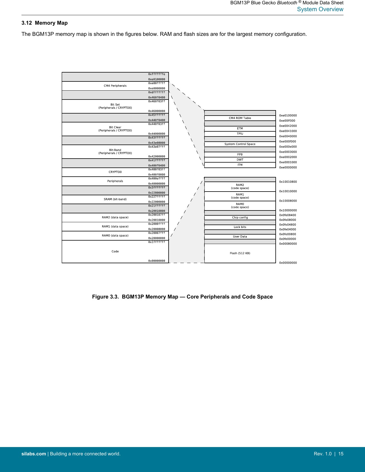
![Figure 3.4. BGM13P Memory Map — Peripherals3.13 Configuration SummaryThe features of the BGM13P are a subset of the feature set described in the device reference manual. The table below describes de-vice specific implementation of the features. Remaining modules support full configuration.Table 3.3. Configuration SummaryModule Configuration Pin ConnectionsUSART0 IrDA SmartCard US0_TX, US0_RX, US0_CLK, US0_CSUSART1 IrDA I2S SmartCard US1_TX, US1_RX, US1_CLK, US1_CSUSART2 IrDA SmartCard US2_TX, US2_RX, US2_CLK, US2_CSTIMER0 with DTI TIM0_CC[2:0], TIM0_CDTI[2:0]TIMER1 - TIM1_CC[3:0]WTIMER0 with DTI WTIM0_CC[2:0], WTIM0_CDTI[2:0]BGM13P Blue Gecko Bluetooth ® Module Data SheetSystem Overviewsilabs.com | Building a more connected world. Rev. 1.0 | 16](https://usermanual.wiki/Silicon-Laboratories-Finland/BGM13P.Installation-Instructions/User-Guide-3756753-Page-16.png)
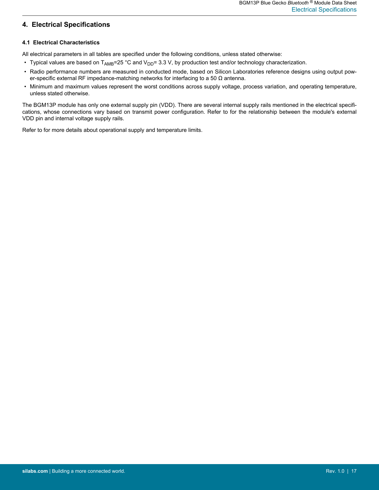


![10. Tape and Reel Specifications10.1 Tape and Reel SpecificationThis section contains information regarding the tape and reel packaging for the BGM13P Blue Gecko Bluetooth ® Module.10.2 Reel Material and Dimensions• Reel material: Polystyrene (PS)• Reel diameter: 13 inches (330 mm)• Number of modules per reel: 1000 pcs• Disk deformation, folding whitening and mold imperfections: Not allowed• Disk set: consists of two 13 inch (330 mm) rotary round disks and one central axis (100 mm)• Antistatic treatment: Required•Surface resistivity: 104 - 109 Ω/sq.Figure 10.1. Reel Dimension — Side ViewSymbol Dimensions [mm]W0 44.0 +0.5/-.0.0W1 48.0BGM13P Blue Gecko Bluetooth ® Module Data SheetTape and Reel Specificationssilabs.com | Building a more connected world. Rev. 1.0 | 85](https://usermanual.wiki/Silicon-Laboratories-Finland/BGM13P.Installation-Instructions/User-Guide-3756753-Page-85.png)
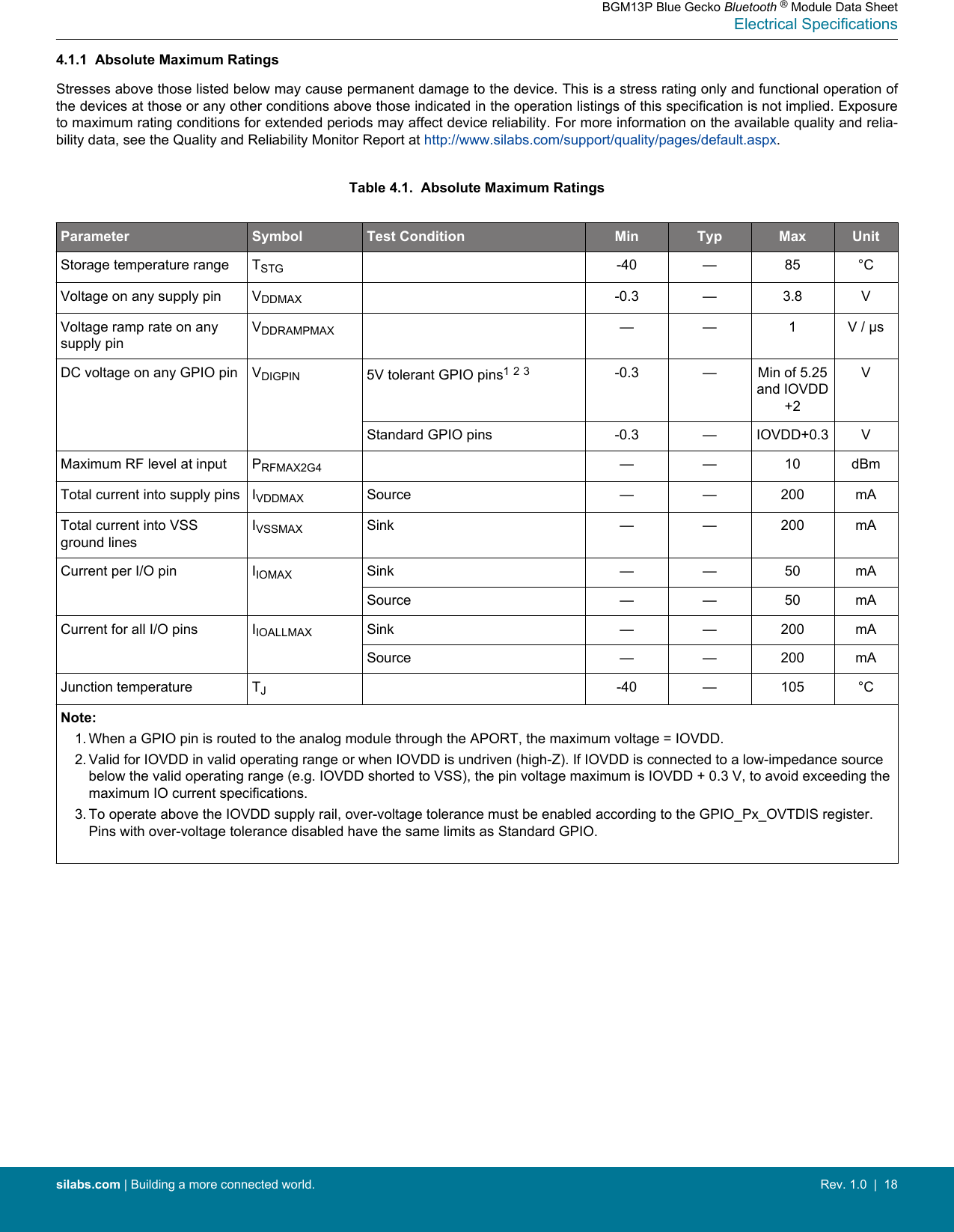
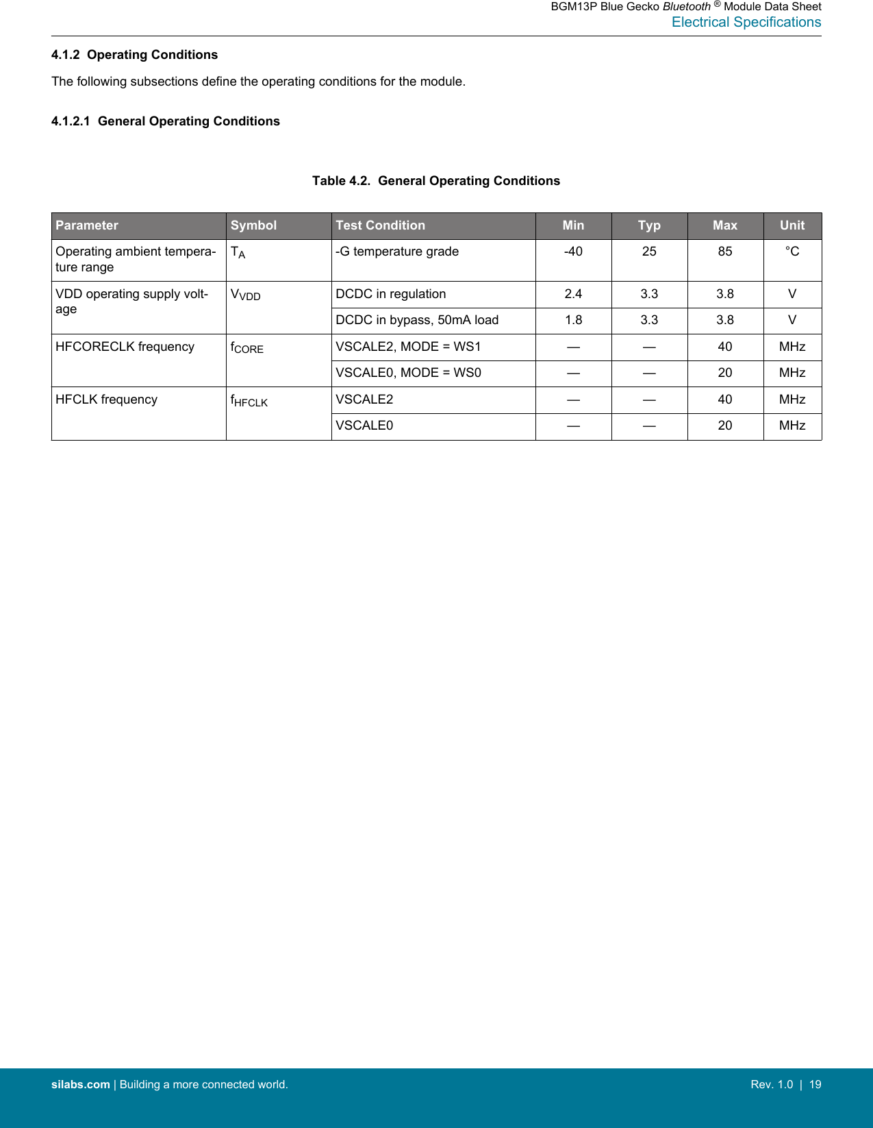
![10.3 Module Orientation and Tape FeedThe user direction of feed, start and end of tape on reel and orientation of the modules on the tape are shown in the figure below.Figure 10.2. Module Orientation and Feed Direction10.4 Cover Tape InformationFigure 10.3. Cover Tape InformationSymbol Dimensions [mm]Thickness (T) 0.055 +0.005/-0.003Width (W) 37.50 +0.30/-0.10BGM13P Blue Gecko Bluetooth ® Module Data SheetTape and Reel Specificationssilabs.com | Building a more connected world. Rev. 1.0 | 86](https://usermanual.wiki/Silicon-Laboratories-Finland/BGM13P.Installation-Instructions/User-Guide-3756753-Page-86.png)