Silicon Laboratories Finland EM358L ETRX3581-LRS, ETRX3582-LRS, ETRX3585-LRS, ETRX3586-LRS, ETRX3587-LRS, ETRX3588-LRS, ETRX3581HR-LRS, ETRX3582HR-LRS, ETRX3585HR-LRS, ETRX3586HR-LRS, ETRX3587HR-LRS, ETRX3588HR-LRS User Manual TG PM 0511 ETRX358x LRS r2
Telegesis (UK) Ltd ETRX3581-LRS, ETRX3582-LRS, ETRX3585-LRS, ETRX3586-LRS, ETRX3587-LRS, ETRX3588-LRS, ETRX3581HR-LRS, ETRX3582HR-LRS, ETRX3585HR-LRS, ETRX3586HR-LRS, ETRX3587HR-LRS, ETRX3588HR-LRS TG PM 0511 ETRX358x LRS r2
User Manual
Telegesis
TG-PM-0511-ETRX358x-LRS r2
ETRX358x-LRS and ETRX358xHR-LRS Product Manual
©2014 Telegesis (UK) Ltd ETRX358x-LRS Product Manual
ETRX358x-LRS ZIGBEE
®
MODULES
PRODUCT MANUAL

ETRX358x-LRS and ETRX358xHR-LRS
©2014 Telegesis (UK) Ltd - 2 - ETRX358x-LRS Product Manual
Table of Contents
1 INTRODUCTION ................................................................................................................. 5
1.1 Hardware Description ....................................................................................................... 5
2 PRODUCT APPROVALS ................................................................................................... 7
2.1 FCC Approvals ................................................................................................................. 7
2.1.1 FCC Labelling Requirements ........................................................................................... 8
2.2 IC (Industry Canada) Approvals ....................................................................................... 8
2.2.1 IC Labelling Requirements ............................................................................................... 9
2.3 European Certification .................................................................................................... 10
2.4 Declarations of Conformity ............................................................................................. 10
2.5 IEEE 802.15.4 ................................................................................................................ 10
2.6 The ZigBee Protocol ...................................................................................................... 11
3 MODULE PINOUT ............................................................................................................ 12
4 HARDWARE DESCRIPTION ............................................................................................ 14
4.1 Hardware Interface ......................................................................................................... 14
5 FIRMWARE DESCRIPTION ............................................................................................. 15
5.1 Token Settings ............................................................................................................... 16
5.2 Custom Firmware ........................................................................................................... 16
5.3 Boost Mode vs. Normal Mode ........................................................................................ 16
5.4 Software Interface .......................................................................................................... 17
6 ABSOLUTE MAXIMUM RATINGS ................................................................................... 18
6.1 Environmental Characteristics ........................................................................................ 18
6.2 Recommended Operating Conditions............................................................................. 18
7 DC ELECTRICAL CHARACTERISTICS ........................................................................... 19
8 DIGITAL I/O SPECIFICATIONS ....................................................................................... 21
9 A/D CONVERTER CHARACTERISTICS .......................................................................... 22
10 AC ELECTRICAL CHARACTERISTICS ........................................................................... 22
10.1 TX Power Characteristics ............................................................................................... 24
10.2 Power Settings for Regulatory Compliance .................................................................... 25
10.3 Temperature behaviour .................................................................................................. 26
11 PHYSICAL DIMENSIONS ................................................................................................. 27
12 RECOMMENDED REFLOW PROFILE ............................................................................. 28
13 PRODUCT LABEL DRAWING ......................................................................................... 29
14 RECOMMENDED FOOTPRINT ........................................................................................ 30
14.1 Recommended Placement ............................................................................................. 32
14.2 Example carrier board .................................................................................................... 34
15 RELIABILITY TESTS ........................................................................................................ 35

ETRX358x-LRS and ETRX358xHR-LRS
©2014 Telegesis (UK) Ltd - 3 - ETRX358x-LRS Product Manual
16 APPLICATION NOTES ..................................................................................................... 35
16.1 Safety Precautions ......................................................................................................... 35
16.2 Design Engineering Notes .............................................................................................. 35
16.3 Storage Conditions ......................................................................................................... 36
17 PACKAGING .................................................................................................................... 37
17.1 Embossed Tape ............................................................................................................. 37
17.2 Component Orientation .................................................................................................. 38
17.3 Reel Dimensions ............................................................................................................ 38
17.4 Packaging ...................................................................................................................... 39
18 ORDERING INFORMATION ............................................................................................. 40
19 TRADEMARKS ................................................................................................................. 41
20 DISCLAIMER .................................................................................................................... 41
21 ROHS DECLARATION ..................................................................................................... 41
22 DATA SHEET STATUS .................................................................................................... 41
23 LIFE SUPPORT POLICY .................................................................................................. 41
24 RELATED DOCUMENTS ................................................................................................. 42
25 CONTACT INFORMATION ............................................................................................... 42
ETRX358x-LRS and ETRX358x-LRS
©2014 Telegesis (UK) Ltd - 4 - ETRX358x-LRS Product Manual
The Telegesis ETRX358x-LRS and ETRX358xHR-LRS
modules are low power 2.4GHz ZigBee modules with an added
frontend module (SiGe SE2432L) containing both PA and LNA
for highest possible link budget.
Based on the latest Ember EM358x family of single chip ZigBee
solutions the new long range modules are footprint compatible
with the entire Telegesis ETRX3 family, thus representing a
drop-in replacement for all applications where a high link
budget is required.
The module’s unique AT-style command line interface allows
designers to quickly integrate ZigBee technology without
complex software engineering. For custom application
development the ETRX358x series integrates with ease into
Ember’s InSight development environment.
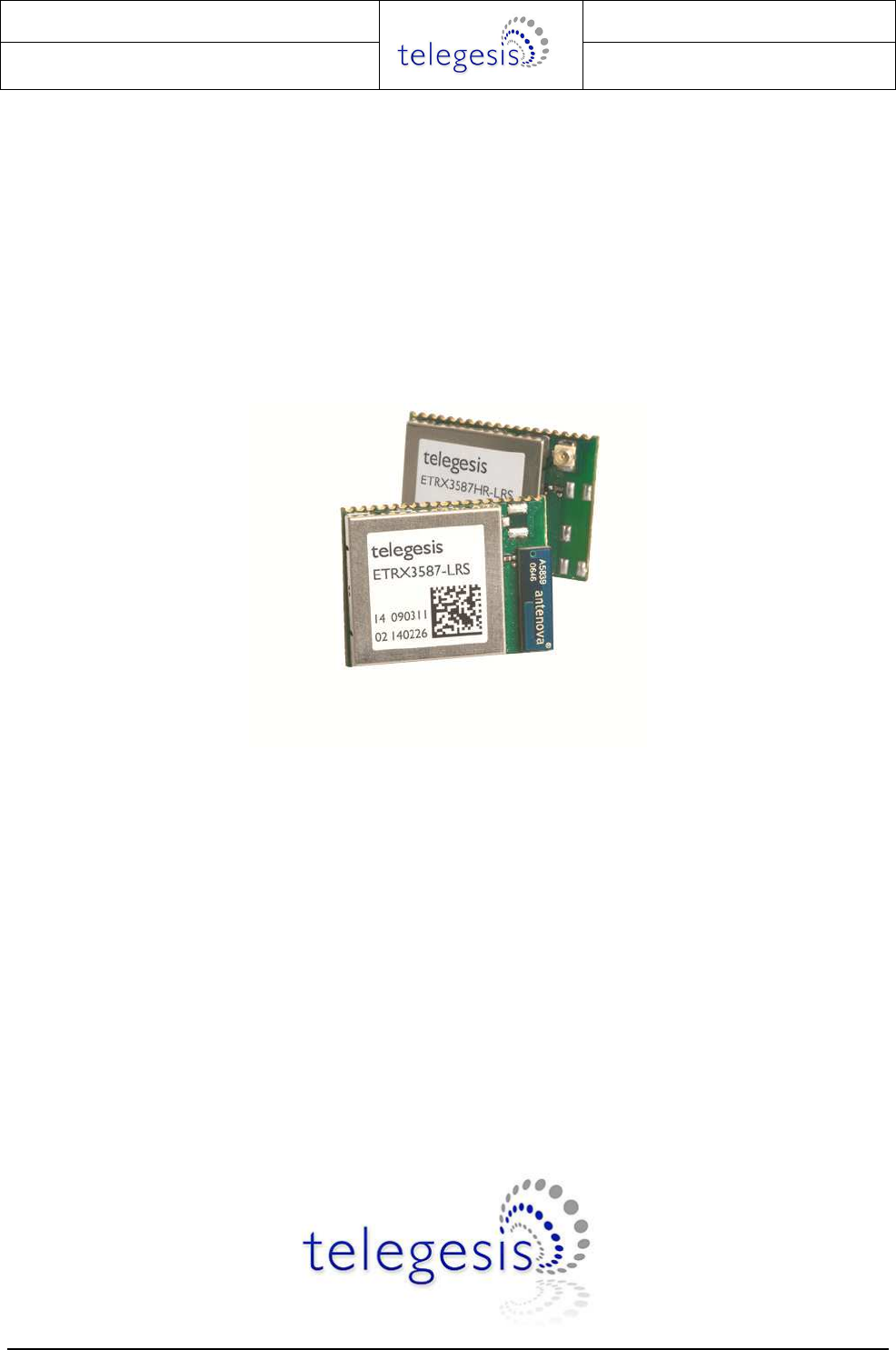
Image not shown actual size; enlarged to show detail.
Module Features
• Small form factor, SMT module 25mm x 19mm
• Same footprint and pin-out as ETRX357-LRS
• Side Castellations for easy soldering and inspection
• Two antenna options: Integrated chip antenna or U.FL
coaxial connector
• Based on 32-bit ARM® Cortex-M3
• Industry standard JTAG Programming and real time
network level debugging via the Ember Debug Port
• Up to 512kB of flash and 64kbytes of RAM
• Lowest Deep Sleep Current of sub 1µA with retained
RAM and GPIO and multiple sleep modes
• Ultra Wide supply voltage range (2.1 to 3.6V)
• Optional 32.768kHz watch crystal can be added
externally
• Module ships with standard Telegesis AT-style
command interface based on the ZigBee PRO feature
set
• Can act as an End Device, Router or Coordinator
• 22 general-purpose I/O lines including analogue inputs
• Firmware upgrades via serial port or over the air
(password protected)
• Hardware supported encryption (AES-128)
• CE and FCC and IC compliance, IC and FCC modular
approval
• Operating temperature range: -40
°
C to +85
°
C
• Standard version without LNA and PA available in the
same form factor
Radio Features
• Based on the Silicon Labs EM358x family of single chip
ZigBee®
SoCs
• 2.4GHz ISM Band
• 250kbit/s over the air data rate – NB: actual usable data
throughput with ZigBee is about 20kbps
• 15 channels (IEEE802.15.4 Channel 11 to 25)
• SiGe SE2432L integrated PA and LNA
• +20dBm output power (adjustable down to -41dBm)
• High sensitivity of -106dBm typ. @ 1% packet error rate
• RX Current: 33mA, TX Current: approx 140mA at
20dBm
•
Robust Wi
-
Fi and Bluetooth coexistence
Suggested Application
s
• ZigBee Smart Energy applications
• Wireless Alarms and Security
• Home/Building Automation
• Wireless Sensor Networks
• M2M Industrial Controls
• Lighting and ventilation control
• Remote monitoring
• Environmental monitoring and control
Development Kit
• Enhancement kit available to upgrade existing
Telegesis and Ember development kits to be used with
the new ETRX358x family
• AT-style software interface command dictionary can be
modified for high volume customers.
• Custom software development available upon request.
Example AT
-
Style Commands
AT+BCAST Send a Broadcast
AT+UCAST:<address> Send a Unicast
AT+EN Establish PAN network
AT+JN Join PAN
At power-up the last configuration is loaded from non-
volatile S-Registers, which can eliminate the need for an
additional host controller.
ETRX358x-LRS and ETRX358x-LRS
©2014 Telegesis (UK) Ltd - 5 - ETRX358x-LRS Product Manual
1 Introduction
This document describes the Telegesis ETRX358x-LRS and ETRX358xHR-LRS ZigBee long
range modules which have been designed to be easily integrated into another device and to
provide a fast, simple and low cost wireless mesh networking interface.
The Telegesis ETRX3 series modules are based on the Silicon Labs ZigBee compliant platform
consisting of the single chip family of EM358x SoCs combined with the ZigBee PRO compliant
EmberZNet meshing stack. Integration into a wide range of applications is made easy using a
simple AT style command interface and advanced hardware design.
The configurable functionality of the Telegesis AT Commandset often allows the ETRX3 series
ZigBee modules to be used without an additional host microcontroller saving even more integration
time and costs. In addition to the Telegesis AT Commandset, the ETRX358x-LRS and
ETRX358xHR-LRS modules can be used with custom-built firmware whilst representing an ideal
platform for custom firmware development in conjunction with the Silicon Labs ZigBee
development kits.
No RF experience or expertise is required to add this powerful wireless networking capability to
your products. The ETRX358x-LRS and ETRX358xHR-LRS offer fast integration opportunities
and the shortest possible time to market for your product.
1.1 Hardware Description
The main building blocks of the ETRX358x-LRS and ETRX358xHR-LRS are the single chip
EM358x SoC from Silicon Labs, a SiGe SE2432L frontend module combining a Power Amplifier
with a Low Noise Amplifier, a 24MHz reference crystal and RF front-end circuitry optimized for best
RF performance. The modules are available with on-board antenna or alternatively a U.FL
connector for attaching external antennae. Modules with the U.FL connector are identified by the
“HR” suffix.
The integrated antenna is an Antenova Rufa, and details of the radiation pattern and further data
are available from the Antenova website [5].
Module
Chip
Flash
RAM
Antenna
USB
ETRX3581-LRS
1
EM3581 256kB 32kB Chip No
ETRX3581HR-LRS
1
EM3581 256kB 32kB External No
ETRX3582-LRS
1
EM3582 256kB 32kB Chip Yes
ETRX3582HR-LRS
1
EM3582 256kB 32kB External Yes
ETRX3585-LRS
1
EM3585 512kB 32kB Chip No
ETRX3585HR-LRS
1
EM3585 512kB 32kB External No
ETRX3586-LRS
1
EM3586 512kB 32kB Chip Yes
ETRX3586HR-LRS
1
EM3586 512kB 32kB External Yes
ETRX3587
-LRS
EM3587
512kB
64kB
Chip
No
ETRX3587HR
-LRS
EM3587
512kB
64kB
External
No
ETRX3588-LRS
1
EM3588 512kB 64kB Chip Yes
ETRX3588HR
1
EM3588 512kB 64kB External Yes
Table 1: Memories
1
MOQ and Lead Time applies. Only stocked modules are ETRX3587 and ETRX3587HR

ETRX358x-LRS and ETRX358x-LRS
©2014 Telegesis (UK) Ltd - 6 - ETRX358x-LRS Product Manual
The LNA and RF power amplifier of the LRS devices improve the output power by 12dB and the
sensitivity by 5dB which will increase the range by approximately 700% relative to the standard
devices (where local regulations permit the use of the maximum output power).
The ETRX358x and ETRX358xHR are used for ZigBee
(www.zigbee.org) applications. In case it is
desired to develop custom firmware instead of using the pre-loaded AT-Command interface, the
Silicon Labs toolchain, consisting of Ember Desktop together with a comprehensive integrated
development environment (IDE), is required.
ETRX358x-LRS and ETRX358x-LRS
©2014 Telegesis (UK) Ltd - 7 - ETRX358x-LRS Product Manual
2 Product Approvals
The ETRX358x-LRS and ETRX358xHR-LRS have been designed to meet all national regulations
for world-wide use. In particular the following certifications have been obtained:
2.1 FCC Approvals
The Telegesis ETRX358x-LRS family with integrated Antenna as well as the ETRX358xHR-LRS
family including the antennas listed in able 2 and the power levels listed in section 10.2 have been
tested to comply with FCC CFR Part 15 (USA) The devices meet the requirements for modular
transmitter approval as detailed in the FCC public notice DA00.1407.transmitter.
FCC statement:
This device complies with Part 15 of the FCC rules. Operation is subject to the following
two conditions: (1) this device may not cause harmful interference, and (2) this device must
accept any interference received, including interference that may cause undesired
operation.
This module complies with the USA SAR requirements and is not intended to be operated within
20cm of the body. The following statement must be included as a CAUTION statement in manuals
for OEM products to alert users on FCC RF exposure compliance
“WARNING: To satisfy FCC RF exposure requirements for mobile transmitting devices, a
separation distance of 20cm or more should be maintained between the antenna of this
device and persons during operation. To ensure compliance, operations at closer
distances than this are not recommended.”
Item
Part No.
Manufacturer
Type
Impedance
Gain
1 BT-Stubby
(straight) EAD Ltd. [6] ¼ Wave 50Ω 0dBi
2 BT-Stubby
(right-angle) EAD Ltd. [6] ¼ Wave 50Ω 0dBi
3 CJ-2400-6603 Chang Jia ½ Wave 50 Ω 2.0dBi
4 Rufa (on
board) Antenova Chip 50Ω 2.1dBi
(peak)
Table 2. Approved Antennae
An end user deploying an ETRX358x-LRS or an ETRX358xHR-LRS module together with an
antenna as listed in Table 2 is not required to obtain a new authorization for the module – BUT this
does not preclude the possibility that some other form of authorization or testing may be required
for the end product depending upon local territorial regulations.
The FCC requires the user to be notified that any changes or modifications made to this device
that are not expressly approved by Telegesis (UK) Ltd. may void the user's authority to operate the
equipment.
When using the ETRX358x-LRS with approved antennae, it is required to prevent end-users from
replacing them with non-approved ones.
FCC ID
:
S4
GEM358L

ETRX358x-LRS and ETRX358x-LRS
©2014 Telegesis (UK) Ltd - 8 - ETRX358x-LRS Product Manual
The antenna(s) must be installed such that a minimum separation distance of 20cm is maintained
between the radiator (antenna) and all persons at all times.
2.1.1 FCC Labelling Requirements
When integrating the ETRX358x-LRS or ETRX358xHR-LRS families into a product it must be
ensured that the FCC labelling requirements are met. This includes a clearly visible label on the
outside of the finished product specifying the Telegesis FCC identifier (FCC ID: S4GEM358L) as
well as the notice above. This exterior label can use wording such as “Contains Transmitter
Module FCC ID: S4GEM358L” or “Contains FCC ID: S4GEM358L” although any similar wording
that expresses the same meaning may be used.
2.2 IC (Industry Canada) Approvals
The Telegesis ETRX358x-LRS family with integrated Antenna as well as the ETRX358xHR-LRS
family have been approved by Industry Canada to operate with the antenna types listed in Table 2
with the maximum permissible gain and required antenna impedance for each antenna type
indicated. Antenna types not included in this list, having a gain greater than the maximum gain
indicated for that type, are strictly prohibited for use with this device.
IC-ID: 8735A-EM358L
• This device complies with Industry Canada license-exempt RSS standard(s). Operation is
subject to the following two conditions: (1) this device may not cause interference, and (2)
this device must accept any interference, including interference that may cause undesired
operation of the device.
• Under Industry Canada regulations, this radio transmitter may only operate using an antenna
of a type and maximum (or lesser) gain approved for the transmitter by Industry Canada. To
reduce potential radio interference to other users, the antenna type and its gain should be so
chosen that the equivalent isotropically radiated power (e.i.r.p.) is not more than that
permitted for successful communication.
• To comply with Industry Canada RF radiation exposure limits for general population, the
antenna(s) used for this transmitter must be installed such that a minimum separation
distance of 20cm is maintained between the radiator (antenna) and all persons at all times
and must not be co-located or operating in conjunction with any other antenna or transmitter
• This device has been designed to operate with the antennas listed in Table 2, and having a
maximum gain of 2.1 dBi. Antennas not included in this list or having a gain greater than 2.1
dBi are strictly prohibited for use with this device. The required antenna impedance is 50
ohms.
French Statements
• Conformément à la réglementation d'Industrie Canada, le présent émetteur radio peut
fonctionner avec une antenne d'un type et d'un gain maximal (ou inférieur) approuvé pour
l'émetteur par Industrie Canada. Dans le but de réduire les risques de brouillage
radioélectrique à l'intention des autres utilisateurs, il faut choisir le type d'antenne et son gain

ETRX358x-LRS and ETRX358x-LRS
©2014 Telegesis (UK) Ltd - 9 - ETRX358x-LRS Product Manual
de sorte que la puissance isotrope rayonnée équivalente (p.i.r.e.) ne dépasse pas l'intensité
nécessaire à l'établissement d'une communication satisfaisante.
• Le présent appareil est conforme aux CNR d'Industrie Canada applicables aux appareils
radio exempts de licence. L'exploitation est autorisée aux deux conditions suivantes : (1)
l'appareil ne doit pas produire de brouillage, et (2) l'utilisateur de l'appareil doit accepter tout
brouillage radioélectrique subi, même si le brouillage est susceptible d'en compromettre le
fonctionnement.
OEM Responsibilities
The ETRX358x-LRS and ETRX358x-LRS families of module have been certified for integration into
products only by OEM integrators under the following conditions:
1. The antenna(s) must be installed such that a minimum separation distance of 20cm is
maintained between the radiator (antenna) and all persons at all times.
2. The transmitter module must not be co-located or operating in conjunction with any other
antenna or transmitter.
As long as the two conditions above are met, further transmitter testing will not be required.
However, the OEM integrator is still responsible for testing their end-product for any additional
compliance requirements required with this module installed (for example, digital device emissions,
PC peripheral requirements, etc.).
IMPORTANT NOTE: In the event that these conditions can not be met (for certain configurations
or co-location with another transmitter), then Industry Canada certification is no longer considered
valid and the IC Certification Number can not be used on the final product. In these circumstances,
the OEM integrator will be responsible for re-evaluating the end product (including the transmitter)
and obtaining a separate Industry Canada authorization.
2.2.1 IC Labelling Requirements
The ETRX358x-LRS and ETRX358xHR-LRS family modules are labelled with its own IC Certification
Number. If the IC Certification Number is not visible when the module is installed inside another device,
then the outside of the device into which the module is installed must also display a label referring to the
enclosed module. In that case, the final end product must be labelled in a visible area with the following:
“Contains Transmitter Module IC: 8735A-EM358L”
or
“Contains IC: 8735A-EM358L”
The OEM of the ETRX358x-LRS and ETRX358xHR-LRS family modules must only use the approved
antenna(s) listed above, which have been certified with this module.
The OEM integrator has to be aware not to provide information to the end user regarding how to
install or remove this RF module or change RF related parameters in the user’s manual of the end
product.
ETRX358x-LRS and ETRX358x-LRS
©2014 Telegesis (UK) Ltd - 10 - ETRX358x-LRS Product Manual
2.3 European Certification
The ETRX358x and ETRX358xHR families are at a maximum power level of 21.15mW e.i.r.p.
(13.2dBm) compliant to the following standards:
• Radio: EN 300 328:V1.8.1
• EMC: EN 301 489-17:V2.2.1
• Safety: EN 60950-1:2006/A12:2011
All tests have been conducted with the antennae listed in Table 2.
If the ETRX358x-LRS and ETRX358xHR-LRS families of modules are incorporated into an OEM
product, the OEM product manufacturer must ensure compliance of the final product to the
European Harmonised EMC, and low voltage/safety standards. A Declaration of Conformity must
be issued for each of these standards and kept on file as described in the R&TTE Directive. The
final product must not exceed the specified power ratings, antenna specifications and installation
requirements as specified in this user manual. If any of these specifications are exceeded in the
final product then a submission must be made to a notified body for compliance testing to all of the
required standards.
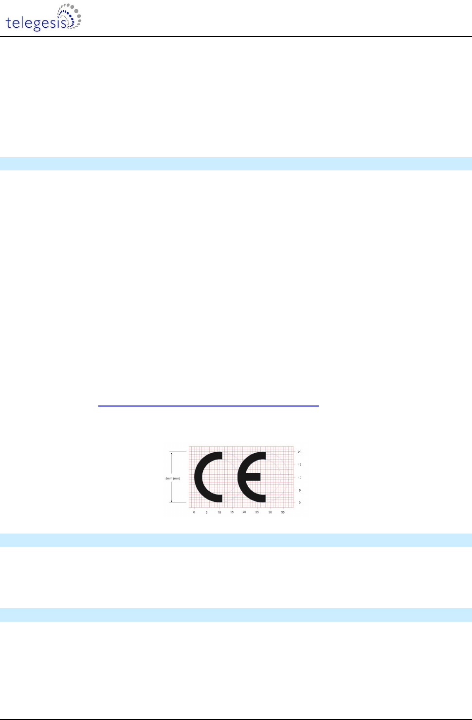
The ‘CE’ marking must be applied to a visible location on any OEM product. For more information
please refer to http://ec.europa.eu/enterprise/faq/ce-mark.htm. Customers assume full
responsibility for learning and meeting the required guidelines for each country in their distribution
market.
2.4 Declarations of Conformity
Telegesis (UK) Ltd has issued Declarations of Conformity for all ETRX3 series ZigBee RF
Modules, which cover Radio Emissions, EMC and Safety. These documents will be available from
our website or on request
2.5 IEEE 802.15.4
IEEE 802.15.4 is a standard for low data rate, wireless networks (raw bit-rate within a radio packet
of 250kbps @2.4GHz) which focuses on low cost, low duty cycle, long primary battery life
applications as well as mains-powered applications. It is the basis for the open ZigBee Protocol.

ETRX358x-LRS and ETRX358x-LRS
©2014 Telegesis (UK) Ltd - 11 - ETRX358x-LRS Product Manual
2.6 The ZigBee Protocol
The ZigBee Protocol is a set of standards for wireless connectivity for use between any devices
over short to medium distances. The specification was originally ratified in December 2004, paving
the way for companies to start making low-power networks a reality.
ZigBee uses an IEEE 802.15.4 radio specification running on the 2.4GHz band, plus three
additional layers for networking, security and applications. What makes the specification unique is
its use of a mesh network architecture which, in bucket chain style, passes data from one node to
the next until it lands at its destination. The network is self-healing and adapts its routing as link
quality changes or nodes move. Furthermore, nodes can be defined as End Devices which do not
act as routers, but can therefore be put into a low-power sleep state.
The enhanced version of the ZigBee standard (or ZigBee 2006) was released in December 2006,
adding new features and improvements to the only global wireless communication standard
enabling the development of easily deployable low-cost, low-power, monitoring and control
products for homes, commercial buildings and industrial plant monitoring. In 2007 the ZigBee
Alliance introduced the PRO feature-set which offers advantages over earlier feature-sets,
including
• Truly self-healing mesh networking
• Messages can now travel up to 30 hops
• Source-Routing for improved point to multipoint message transmission
• Improved security including Trust-Centre link keys
• New message types and options
The Telegesis AT Command-set, which by default ships on all ETRX3 series products is based on
the ZigBee PRO feature-set. For more information on the Telegesis AT Command-set please refer
to the separate documentation at www.telegesis.com.
ETRX358x-LRS and ETRX358x-LRS
©2014 Telegesis (UK) Ltd - 12 - ETRX358x-LRS Product Manual
3 Module Pinout
Figure 1. ETRX3 series Module Pinout (top view)
The table below gives details about the pin assignment for direct SMD soldering of the ETRX3
series modules to the application board. For more information on the alternate functions please
refer to [2]. Also refer to the Telegesis AT Command-set documentation to understand how the
pre-programmed firmware makes use of the individual I/Os.
All GND pads are connected within the module, but for best RF performance all of them should be
grounded externally.
ETRX35
8
x
pad
Name
Default
Use
Alternate
function
EM35x
pin
Alternate
functions
1 GND GND GND
2 TX_ACTIVE{1} I/O 11 TX_ACTIVE. PC5 of the EM35x is used to control
the FEM
3 PC6 I/O 13 OSC32B, nTX_ACTIVE
4 PC7 I/O 14 OSC32A, OSC32_EXT
5 PA7 {5} I/O 18 TIM1C4
6 PB3 {2,3} I/O CTS 19 SC1nCTS, SC1SCLK, TIM2C3
7 nReset {5} nReset 12
8 PB4 {2} I/O RTS 20 TIM2C4, SC1nRTS, SC1nSSEL
9 PA0 I/O 21 TIM2C1, SC2MOS,USBDM{7}I
10 PA1 I/O 22 TIM2C3, SC2SDA, SC2MISO,USBDP{7}
11 PA2 I/O 24 TIM2C4, SC2SCL, SC2SCLK
12 PA3 I/O 25 SC2nSSEL, TRACECLK, TIM2C2
13 GND GND GND
14 PA4 I/O 26 ADC4, PTI_EN, TRACEDATA
15 PA5 {4} I/O 27 ADC5, PTI_DATA, nBOOTMODE, TRACEDATA3
16 PA6 {5} I/O 29 TIM1C3
17 PB1{3} TXD 30 SC1MISO, SC1MOSI, SC1SDA, SC1TXD,
TIM2C1
18 PB2{3} RXD 31 SC1MISO, SC1MOSI, SC1SCL, SC1RXD,
TIM2C2

ETRX358x-LRS and ETRX358x-LRS
©2014 Telegesis (UK) Ltd - 13 - ETRX358x-LRS Product Manual
ETRX35
8
x
pad
Name
Default
Use
Alternate
function
EM35x
pin
Alternate
functions
19 GND GND GND
20 GND GND GND
21 JTCK JTCK 32 SWCLK
22 PC2 I/O 33 JTDO, SWO
23 PC3 I/O 34 JTDI
24 PC4 I/O 35 JTMS, SWDIO
25 N/C{1} N/C 36 PB0 of the EM35x is used to control the FEM
26 PC1 I/O ADC3 38 ADC3, SWO, TRACEDATA0
27 PC0 {5} I/O 40 JRST, IRQD, TRACEDATA1
28 PB7 {5} I/O ADC2 41 ADC2, IRQC, TIM1C2
29 PB6 {5} I/O ADC1 42 ADC1, IRQB, TIM1C1
30 PB5 I/O ADC0 43 ADC0, TIM2CLK, TIM1MSK
31 GND GND GND
32 Vcc Vcc Vcc
33 GND GND GND
Table 3. Pin Information
Notes:
{1} Pins PB0 and PC5 of the EM357 are used internally to control the front-end module. PB0 is not
available to the user.
{2} The serial UART connections TXD, RXD, CTS and RTS are PB1, PB2, PB3 and PB4 respectively
{3} When using the Telegesis AT Command-set, RTS/CTS handshaking is selectable in firmware. See
the AT Command Manual.
{4} If PA5 is driven low at power-up or reset the module will boot up in the bootloader
{5} PA6, PA7, PB6, PB7 and PC0 can drive high current (see section 8)
{6} nRESET is level-sensitive, not edge-sensitive. The module is held in the reset state while nRESET
is low. This signal has a 30kΩ Pull-Up.
{7} ETRX3588, ETRX3586, ETRX3582 and ETRX3588HR, ETRX3586HR, ETRX3582HR variants only
Alternate functions depend on the firmware, but the Telegesis R3xx AT Command-set functions
are indicated here for convenience.
Important Note: The ETRX358x series and the ETRX358x-LRS series of modules are footprint
compatible, but on the ETRX358x-LRS series pins PB0 and PC5 of the EM358x are used
internally to control the front-end module and are not available to the user. PC5 is still available on
Pad2, but it is configured as TX_ACTIVE signal and cannot be used as a general purpose GPIO.
See also the table “Module pads and functions” in the ETRX357 Development Kit Product Manual.
Refer to the Silicon Labs EM358x manual for details of the alternate functions and pin names.
ETRX358x-LRS and ETRX358x-LRS
©2014 Telegesis (UK) Ltd - 14 - ETRX358x-LRS Product Manual
4 Hardware Description
24MHz
EM358x
I/O
UART
I / O
programming
5
JTAG
V
cc
V
reg
RESET
RESET
Match
integrated
antenna
U.FL socket
rf
terminal
selection,
filtering and
matching
circuitry
LDO
1V8
1,8Vdc
A/D
LDO
1V25
Match
FEM
USB*
*not available on all Types
Figure 2. Hardware Diagram
The ETRX358x-LRS and ETRX358x-LRS are based on the Silicon Labs EM358x family of ZigBee
SoCs in addition to a frontend module containing a PA, LNA and RF switch in addition to the RF-
frontend circuitry. The EM358x family of ZigBee SoCs are fully integrated 2.4GHz ZigBee
transceivers with a 32-bit ARM
®
Cortex M3
TM
microprocessor, flash and RAM memory, and
peripherals.
The industry standard serial wire and JTAG programming and debugging interfaces together with
the standard ARM system debug components help to streamline any custom software
development.
In addition to this a number of MAC functions are also implemented in hardware to help maintain
the strict timing requirements imposed by the ZigBee and IEEE802.15.4 standards.
The new advanced power management features allow faster wakeup from sleep and new power-
down modes allow this 3
rd
generation module to offer a longer battery life than any 2
nd
generation
modules on the market.
The EM358x has fully integrated voltage regulators for both required 1.8V and 1.25V supply
voltages. The voltages are monitored (brown-out detection) and the built in power-on-reset circuit
eliminates the need for any external monitoring circuitry. A 32.768kHz watch crystal can be
connected externally to pads 3 and 4 in case more accurate timing is required.
4.1 Hardware Interface
All GPIO pins of the EM358x chips are accessible on the module’s pads. Whether signals are
used as general purpose I/Os, or assigned to a peripheral function like ADC is set by the firmware.
When using the Telegesis AT Commandset please refer to the AT Commandset manual and the
development kit manual for this information and when developing custom firmware please refer to
the EM358x datasheet [2].

ETRX358x-LRS and ETRX358x-LRS
©2014 Telegesis (UK) Ltd - 15 - ETRX358x-LRS Product Manual
5 Firmware Description
By default, the modules will be pre-loaded with a standalone bootloader which supports over-the-
air bootloading as well as serial bootloading of new firmware.
In order to enter the standalone bootloader using a hardware trigger pull PA5 to ground and
power-cycle or reset the module. To avoid entering the standalone bootloader unintentionally
make sure not to pull this pin down during boot-up unless the resistance to ground is >10kΩ. (A
pull-up is not required).
In addition to the standalone bootloader the modules also contain the current release of the
Telegesis AT-style command interface as described in the Telegesis AT command dictionary and
the Telegesis user guide. Check www.telegesis.com for updates. Each module comes with a
unique 64-bit 802.15.4 identifier which is stored in non-volatile memory. The commands and
responses pass through the serial port of the ETRX358x as ASCII text, so a simple terminal
application will usually suffice. We provide Telegesis Terminal for interaction with the module but it
is not an essential feature.
The pre-loaded AT-style command interface firmware is based on the EmberZNet PRO meshing
stack which implements routers/coordinators as well as (sleepy) end devices. [End devices have
no routing responsibility and therefore are allowed to go to sleep, whilst still being able to send and
receive messages via a parent router. In addition to classical sleepy and non-sleepy end devices
the module firmware also supports mobile (sleepy) end devices capable of changing their parent
quickly whenever they change their position within the network.]
A router is typically a mains powered device whilst a sleepy end device (SED) can be battery
powered.
The module is also able to act as a coordinator and Trust Centre through external host control.
The AT style command line supplies all the tools required to set up and manage a ZigBee network
by allowing easy access to the low-level functionality of the stack.
The Telegesis firmware uses the meshing and self-healing EmberZNet PRO stack to overcome
many of the limitations of the tree network topology of the ZigBee 2006 stack by using the ZigBee
PRO featureset.
The Telegesis firmware allows low-level access to physical parameters such as channel and
power level. Parameters that define the functionality of the ETRX358x module and also allow
standalone functionality are saved in non-volatile memory organised in so-called S-Registers. The
SPI and I2C buses are not supported by the current firmware release, but can be used with custom
firmware.
ETRX358x-LRS and ETRX358x-LRS
©2014 Telegesis (UK) Ltd - 16 - ETRX358x-LRS Product Manual
5.1 Token Settings
The ETRX358x-LRS Series Modules’ manufacturing tokens will be pre-programmed with the
settings shown in the table below.
Token Description TG Default
MFG_CIB_OBS Option Bytes <not written>
MFG_CUSTOM_VERSION Optional Version Number <not written>
MFG_CUSTOM_EUI_64 Custom EUI <not written>
MFG_STRING Device Specific String TELEGESIS
MFG_BOARD_NAME Hardware Identifier <Order Code>
MFG_MANUF_ID Manufacturer ID 0x1010
MFG_PHY_CONFIG Default Power Settings 0xFFFD
MFG_BOOTLOAD_AES_KEY Bootloader Key <not written>
MFG_EZSP_STORAGE EZSP related <not written>
MFG_CBKE_DATA SE Security <not written>
MFG_INSTALLATION_CODE SE Installation <not written>
MFG_OSC24M_BIAS_TRIM Crystal Bias <not written>
MFG_SYNTH_FREQ_OFFSET Frequency offset <not written>
MFG_OSC24M_SETTLE_DELAY Crystal Stabilizing Time <not written>
MFG_SECURITY_CONFIG Security Settings <not written>
MFG_CCA_THRESHOLD CCA Threshold 0xFEBF
MFG_SECURE_BOOTLOADER_KEY
Secure Bootloader Key <not written>
Table 4. Manufacturing tokens
5.2 Custom Firmware
For high volume customers the firmware can be customised on request. In addition to this the
ETRX358x-LRS series of modules is an ideal platform for developing custom firmware. In order to
develop custom firmware the Silicon Labs Ember toolchain is required.
When writing firmware for the ETRX358x-LRS it is important to ensure that pins PB0 and PC5 are
correctly configured in order that the RF front-end module can operate correctly. An application
note “Writing customised firmware for the ETRX35x-LRS” can be downloaded from the Telegesis
website.
5.3 Boost Mode vs. Normal Mode
The Ember EM358x chips support a “boost mode” power setting next to the “normal mode” power
setting. The “boost mode” setting increases the sensitivity and output power of the radio
transceiver, however with the LRS variants enabling boost mode has no positive effect on neither
the output power nor the sensitivity and therefore it is recommended to not use boost mode on this
platform. The Telegesis AT Command-set firmware automatically disables boost mode on LRS
series modules and adjusts the power maximum power settings.
Section 10.2 lists the requirements for the maximum power settings for use of the LRS family in
different countries.

ETRX358x-LRS and ETRX358x-LRS
©2014 Telegesis (UK) Ltd - 17 - ETRX358x-LRS Product Manual
5.4 Software Interface
Using the default firmware the ETRX358x-LRS is controlled using a simple AT-style command
interface and (mostly) non-volatile S-Registers. In order to get a full listing of all the available AT-
Commands, please refer to the AT command dictionary document which corresponds to the
firmware revision you intend to use.
In addition to the command dictionary there are user guides explaining the features of the firmware
in more detail. If you need to find out which firmware resides on your module simply type “ATI”
followed by a carriage return and you will be prompted with the module’s manufacturing
information.
The Development Kit manual describes how to upgrade the firmware either via a serial link or over
the air.
ETRX358x-LRS and ETRX358x-LRS
©2014 Telegesis (UK) Ltd - 18 - ETRX358x-LRS Product Manual
6 Absolute Maximum Ratings
No.
Item
Symbol
Absolute Maximum Ratings
Unit
1 Supply voltage V
CC
-0.3 to +3.6 Vdc
2 Voltage on any Pad V
in
-0.3 to V
CC
+0.3 Vdc
3
Voltage on any Pad pin (PA4, PA5, PB5,
PB6, PB7, PC1), when used as an input
to the general purpose ADC with the
low voltage range selected
V
in
-0.3 to +2.0 Vdc
4 Storage temperature range T
stg
-40 to +105 °C
5 Operating temperature range T
op
-40 to +85 °C
6 Input RF level P
max
+6 dBm
8 Reflow temperature T
Death
Please refer to chapter 12 °C
Table 5: Absolute Maximum Ratings
The absolute maximum ratings given above should under no circumstances be violated.
Exceeding one or more of the limiting values may cause permanent damage to the device.
Caution! ESD sensitive device. Precautions should be used when handling the device
in order to prevent permanent damage.
6.1 Environmental Characteristics
No.
Item
Symbol
Absolute Maximum Ratings
Unit
1 ESD on any pad according to
Human Body Model (HBM) circuit
description V
THHBM
±2 kV
2 ESD on non-RF pads according to
Charged Device Model (CDM) circuit
description V
THCDM
±400 V
3 ESD on RF terminal (HBM)
V
THCDM
1000 V
4 Moisture Sensitivity Level MSL MSL3, per J-STD-033
Table 6: Absolute Maximum Ratings
6.2 Recommended Operating Conditions
No.
Item
Condition /
Remark Symbol Value Unit
Min
Typ
Max
1 Supply voltage V
CC
2.1 3.0 3.6 Vdc
2 RF Input Frequency f
C
2405 2480 MHz
3 RF Input Power p
IN
0 dBm
4 Operating temperature
range T
op
-40 +85 °C
Table 7. Recommended Operating Conditions
ETRX358x-LRS and ETRX358x-LRS
©2014 Telegesis (UK) Ltd - 19 - ETRX358x-LRS Product Manual
7 DC Electrical Characteristics
V
CC
= 3.0V, T
AMB
= 25°C, NORMAL MODE (non-Boost) unless otherwise stated
No. Item
Condition /
Remark Symbol Value Unit
Min
Typ
Max
1 Module supply voltage V
CC
2.1 3.6 Vdc
Deep Sleep Current
2 Quiescent current,
internal RC oscillator
disabled, 4kB RAM retained I
SLEEP
1.0 µA
3 Quiescent current,
internal RC oscillator
enabled 4kB RAM retained I
SLEEP
1.25 µA
4 Quiescent current,
including
32.768kHz oscillator 4kB RAM retained I
SLEEP
1.6 µA
5
Quiescent current
including internal RC
oscillator and 32.768kHz
oscillator
4kB RAM retained I
SLEEP
1.9 µA
6 Additional current per
4kB block of RAM
retained I
RAMSLEEP
0,067 µA
Reset Current
7 Quiescent current
nReset asserted I
RESET
2 3 mA
Processor and Peripheral Currents
8 ARM
®
Cortex
TM
M3,
RAM and flash memory 25°C, 12MHz
Core clock I
MCU
7.5 mA
9 ARM
®
Cortex
TM
M3,
RAM and flash memory 25°C, 24MHz
Core clock I
MCU
8.5 mA
10 ARM
®
Cortex
TM
M3,
RAM and flash memory
sleep current
25°C, 12MHz
Core clock I
MCU
4.0 mA
11 ARM
®
Cortex
TM
M3,
RAM and flash memory
sleep current
25°C, 6MHz Core
clock I
MCU
2.5 mA
12 Serial controller current Per serial
controller at max.
clock rate I
SC
0.2 mA
13 General purpose timer
current Per timer at max.
clock rate I
TIM
0.25 mA
14 General purpose ADC
current Max. Sample rate,
DMA I
ADC
1.1 mA
15 USB Active Current I
USB
1 mA
16 USB Suspend Mode
Current I
USBSUSP
2.5 mA
RX Current
17 LNA,Radio receiver MAC
and Baseband ARM
®
Cortex
TM
M3 sleeping. I
RX
26.5 mA
18 Receive current
consumption Total, 12MHz
clock speed I
RX
30 mA
19 Receive current
consumption Total, 24MHz
clock speed I
RX
31.5 mA

ETRX358x-LRS and ETRX358x-LRS
©2014 Telegesis (UK) Ltd - 20 - ETRX358x-LRS Product Manual
TX Current
20 Transmit current
consumption
at +20dBm
module output
power I
TXVCC
140 mA
21 Transmit Current
consumption at min module
output power I
TXVCC
52 mA
Sleep Modes & Peripheral Current
22 MCU, RAM and flash,
FEM, radio off 12MHz clock
speed I
MCU
7 mA
23 MCU, RAM and flash,
FEM, radio off 24MHz clock
speed I
MCU
8 mA
24 Serial Controller Max data rate I
SC
0.2 mA
25 Timer Max clock rate I
TMR
0.25 mA
26 ADC Max sample rate I
ADC
1.1 mA
Table 8: DC Electrical Characteristics
ETRX358x-LRS and ETRX358x-LRS
©2014 Telegesis (UK) Ltd - 21 - ETRX358x-LRS Product Manual
8 Digital I/O Specifications
The digital I/Os of the ETRX358x-LRS module have the ratings shown below.
V
CC
= 3.0V, T
AMB
= 25°C, NORMAL MODE unless otherwise stated
No.
Item
Condition /
Remark Symbol Value Unit
Min
Typ
Max
1 Low Schmitt switching
threshold
Schmitt input
threshold going
from high to low V
SWIL
0.42 x V
CC
0.5 x V
CC
Vdc
2 High Schmitt switching
threshold
Schmitt input
threshold going
from low to high V
SWIH
0.62 x V
CC
0.8 x V
CC
MHz
3 Input current for logic 0 I
IL
-0.5 µA
4 Input current for logic 1 I
IH
0.5 µA
5 Input Pull-up resistor
value R
IPU
24 29 34 kΩ
6 Input Pull-down resistor
value R
IPD
24 29 34 kΩ
7 Output voltage for logic 0 I
OL
= 4mA (8mA) for
standard (high
current) pads V
OL
0 0.18 x V
CC
V
8 Output voltage for logic 1 I
OH
= 4mA (8mA)for
standard (high
current) pads V
OH
0.82 x V
CC
V
CC
V
9 Output Source Current Standard current
pad I
OHS
4 mA
10 Output Sink current Standard current
pad I
OLS
4 mA
11 Output Source Current High current pad (1) I
OHH
8 mA
12 Output Sink current High current pad (1) I
OLH
8 mA
13 Total output current I
OH
+ I
OL
40 mA
Table 9. Digital I/O Specifications
No.
Item
Condition /
Remark Symbol Value Unit
Min
Typ
Max
1 Low Schmitt switching
threshold
Schmitt input
threshold going
from high to low V
SWIL
0.42 x V
CC
0.5 x V
CC
Vdc
2 High Schmitt switching
threshold
Schmitt input
threshold going
from low to high V
SWIH
0.62 x V
CC
0.68 x V
CC
Vdc
3 Input current for logic 0 I
IL
-0.5 µA
4 Input current for logic 1 I
IH
0.5 µA
5 Input Pull-up resistor
value Chip not reset R
IPU
24 29 34 kΩ
6 Input Pull-up resistor
value Chip reset R
IPURESET
12 14.5 17 kΩ
Table 10. nReset Pin Specifications
Notes
1) High current pads are PA6, PA7, PB6, PB7, PC0
ETRX358x-LRS and ETRX358x-LRS
©2014 Telegesis (UK) Ltd - 22 - ETRX358x-LRS Product Manual
9 A/D Converter Characteristics
The ADC is a first-order sigma-delta converter. For additional information on the ADC please refer
to the EM358x datasheet.
No.
Item
1 A/D resolution Up to 14 bits
2 A/D sample time for 7-bit conversion 5.33µs (188kHz)
3 A/D sample time for 14-bit conversion 682µs
4 Reference Voltage 1.2V
Table 11. A/D Converter Characteristics
10 AC Electrical Characteristics
V
CC
= 3.0V, T
AMB
= 25°C, NORMAL MODE measured at 50Ω terminal load connected to the U.FL socket
No.
Receiver
Value
Unit
Min
Typ
Max
1 Frequency range 2400 2500 MHz
2 Sensitivity for 1% Packet Error Rate (PER) -107 -106 -100 dBm
4 Saturation (maximum input level for correct operation) -3 2 dBm
5 High-Side Adjacent Channel Rejection
(1% PER and desired signal –82dBm acc. to [1]) 41 dB
6 Low-Side Adjacent Channel Rejection
(1% PER and desired signal –82dBm acc. to [1]) 40 dB
7 2
nd
High-Side Adjacent Channel Rejection
(1% PER and desired signal –82dBm acc. to [1]) 54 dB
8 2
nd
Low-Side Adjacent Channel Rejection
(1% PER and desired signal –82dBm acc. to [1]) 52 dB
9 Channel Rejection for all other channels
(1% PER and desired signal –82dBm acc. to [1]) tbd dB
10 802.11g rejection centred at +12MHz or –13MHz
(1% PER and desired signal –82dBm acc. to [1]) tbd dB
11 Co-channel rejection
(1% PER and desired signal –82dBm acc. to [1]) tbd dBc
12 Relative frequency error
(2x40ppm required by [1]) -120 120 ppm
13 Relative timing error
(2x40ppm required by [1]) -120 120 ppm
14 Linear RSSI range 35 dB
15 Output power at highest power setting
NORMAL MODE
BOOST MODE
20
20 21
21 21.5
21.5 dBm
16 Output power at lowest power setting -40 dBm
17 Error vector magnitude as per IEEE802.15.4 7 15 %
18 Carrier frequency error -40 40 ppm
Table 12. AC Electrical Characteristics
Please Note: For the relationship between EM358x power settings and module output power
please relate to chapter 10.1 of this document. When developing custom firmware the output
power settings described in this document relate directly to the EM358x power settings accessible
via the Ember stack API. When using the Telegesis AT Command-set firmware the settings
ETRX358x-LRS and ETRX358x-LRS
©2014 Telegesis (UK) Ltd - 23 - ETRX358x-LRS Product Manual
mentioned in this document directly relate to the settings in the S-Register S01 which is used for
setting the output power.
No.
Synthesiser Characteristics
Limit
Unit
Min
Typ
Max
22 Frequency range 2400 2500
MHz
23 Frequency resolution 11.7 kHz
24 Lock time from off state, with correct VCO DAC settings 100 µs
25 Relock time, channel change or Rx/Tx turnaround 100 µs
26 Phase noise at 100kHz offset -71dBc/Hz
27 Phase noise at 1MHz offset -91dBc/Hz
28 Phase noise at 4MHz offset -103dBc/Hz
29 Phase noise at 10MHz offset -111dBc/Hz
Table 13. Synthesiser Characteristics
No.
Power On Reset (POR) Specifications
Limit
Unit
Min
Typ
Max
30 V
CC
POR release 0.62 0.95 1.2 Vdc
31 V
CC
POR assert 0.45 0.65 0.85 Vdc
Table 14. Power On Reset Specifications
No.
nRESET Specifications
Limit
Unit
Min
Typ
Max
32 Reset Filter Time constant 2.1 12 16 µs
33 Reset Pulse width to guarantee a reset 26 µs
34 Reset Pulse width guaranteed not to cause reset 0 1 µs
Table 15. nReset Specifications
ETRX358x-LRS and ETRX358x-LRS
©2014 Telegesis (UK) Ltd - 24 - ETRX358x-LRS Product Manual
10.1 TX Power Characteristics
The diagrams below show the typical output power and module current in dependency on
EM358x-LRS power setting in NORMAL MODE at 3.6V and room temperature.
Figure 3. Output Power vs. Power Setting
Figure 4. Module Current vs. Power Setting
ETRX358x-LRS and ETRX358x-LRS
©2014 Telegesis (UK) Ltd - 25 - ETRX358x-LRS Product Manual
10.2 Power Settings for Regulatory Compliance
Because of the high gain of the frontend module output power of up to 22dBm can be achieved
When the antenna gain is included the output power of the EM358x transceivers needs to be
reduced for regulatory compliance. The following tables list the maximum permitted power setting
for the antenna types listed in Table 2. Note that this is the power out of the EM358x chip (set in
register S01 when using Telegesis R3xx firmware), and the power delivered to the antenna will be
higher by the gain of the RF power amplifier.
(
V
CC
= 3.0V, T
AMB
= 25°C, NORMAL MODE)
Antenna Channels 11-24 Channel 25 Channel 26
1/2 Wave tbd tbd tbd
1/4 Wave tbd tbd tbd
On Board tbd tbd tbd
Table 16: Maximum Power Settings for European Compliance
Finally Table 17 the maximum Power settings for FCC and IC compliance.
Antenna Channels 11-24 Channel 25 Channel 26
1/2 Wave -8 -12 -43
1/4 Wave -8 -8 -26
On Board -7 -7 -26
Table 17: Maximum Power Settings for FCC, IC Compliance
ETRX358x-LRS and ETRX358x-LRS
©2014 Telegesis (UK) Ltd - 26 - ETRX358x-LRS Product Manual
10.3 Temperature behaviour
Figure 5 and Figure 6 illustrate the temperature behaviour of the ETRX358x-LRS series of
modules. Please note that although the temperature behaviour was measured to up to 100
degrees Celsius the absolute maximum rating is 85 degrees Celsius.
Figure 5. Sensitivity vs. Temperature
Figure 6. TX Power vs. Temperature
ETRX358x-LRS and ETRX358x-LRS
©2014 Telegesis (UK) Ltd - 27 - ETRX358x-LRS Product Manual
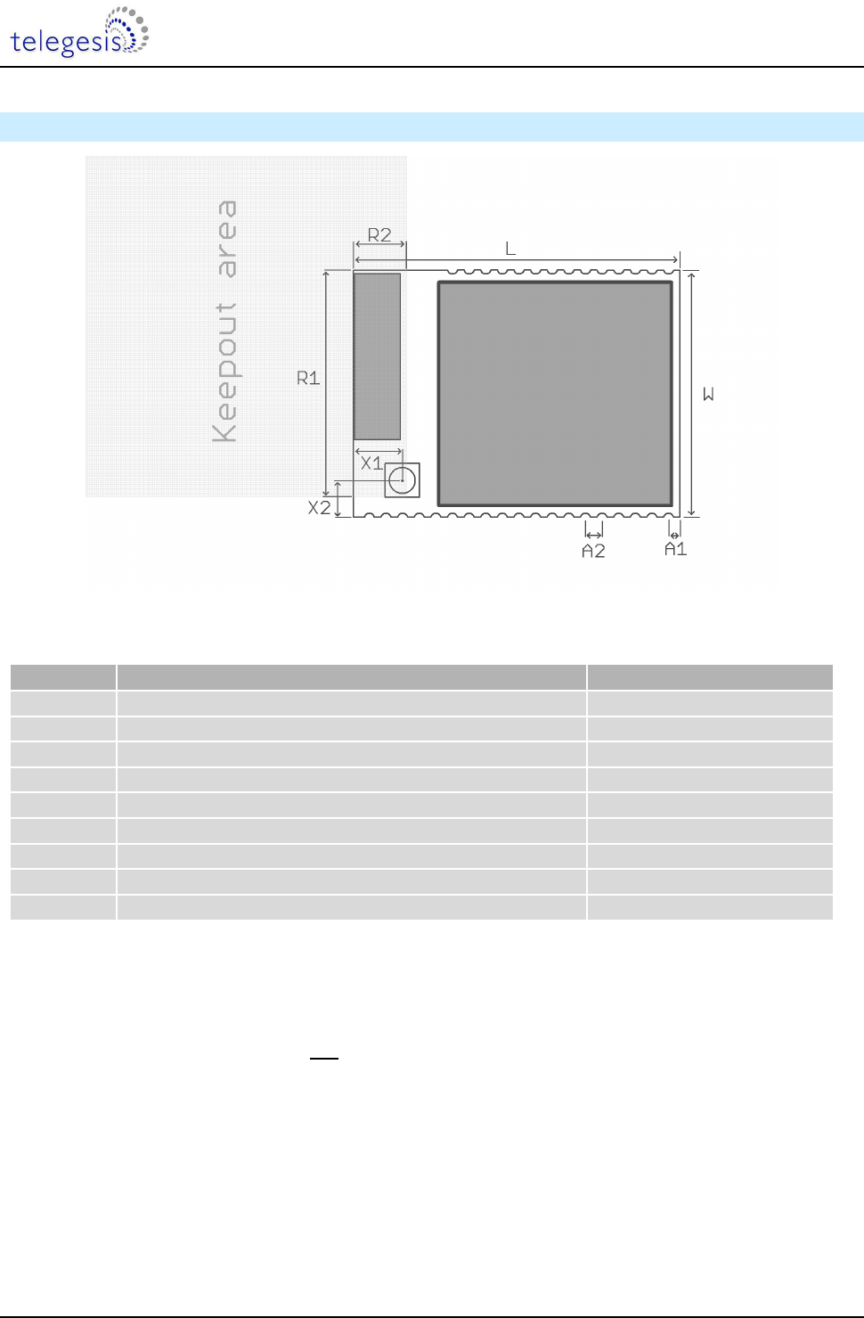
11 Physical Dimensions
Figure 7. ETRX3 Physical Dimensions
Symbol
Explanation
Distance
L Length of the module 25.0mm
W Width of the module 19.0mm
H Height of the module 3.8mm
A1 Distance centre of pad PCB edge 0.9mm
A2 Pitch 1.27mm
R1 Keep-out Zone from corner of PCB 17.5mm
R2 Keep-out Zone from corner of PCB 4.1mm
X1 Distance centre of Antenna connector PCB edge 3.8mm
X2 Distance centre of Antenna connector PCB edge 2.8mm
Table 18. ETRX3 Physical Dimensions
For ideal RF performance when using the on-board antenna, the antenna should be located at the
corner of the carrier PCB. There should be no components, tracks or copper planes in the “keep-
out” area which should be as large as possible. When using the U.FL RF connector the “keep-out”
area does not have to be kept. NB: The modules’ transmit/receive range will depend on the
antenna used and also the housing of the finished product.
ETRX358x-LRS and ETRX358x-LRS
©2014 Telegesis (UK) Ltd - 28 - ETRX358x-LRS Product Manual
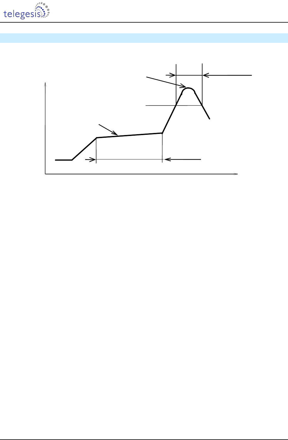
12 Recommended Reflow Profile
Recommended temperature profile
for reflow soldering
Temp
.[°C]
Time [s]
230°C -250°C max.
220°C
150°C – 200°C
90 ±30s
60 +60s-20s
Figure 8. Recommended Reflow Profile
Use of “No-Clean” solder paste is recommended to avoid the requirement for a cleaning process.
Cleaning the module is strongly discouraged because it will be difficult to ensure no cleaning agent
and other residuals are remaining underneath the shielding can as well as in the gap between the
module and the host board.
Please Note:
Maximum number of reflow cycles: 2
Opposite-side reflow is prohibited due to the module’s weight. (i.e. you must not place the
module on the bottom / underside of your PCB and re-flow).
ETRX358x-LRS and ETRX358x-LRS
©2014 Telegesis (UK) Ltd - 29 - ETRX358x-LRS Product Manual
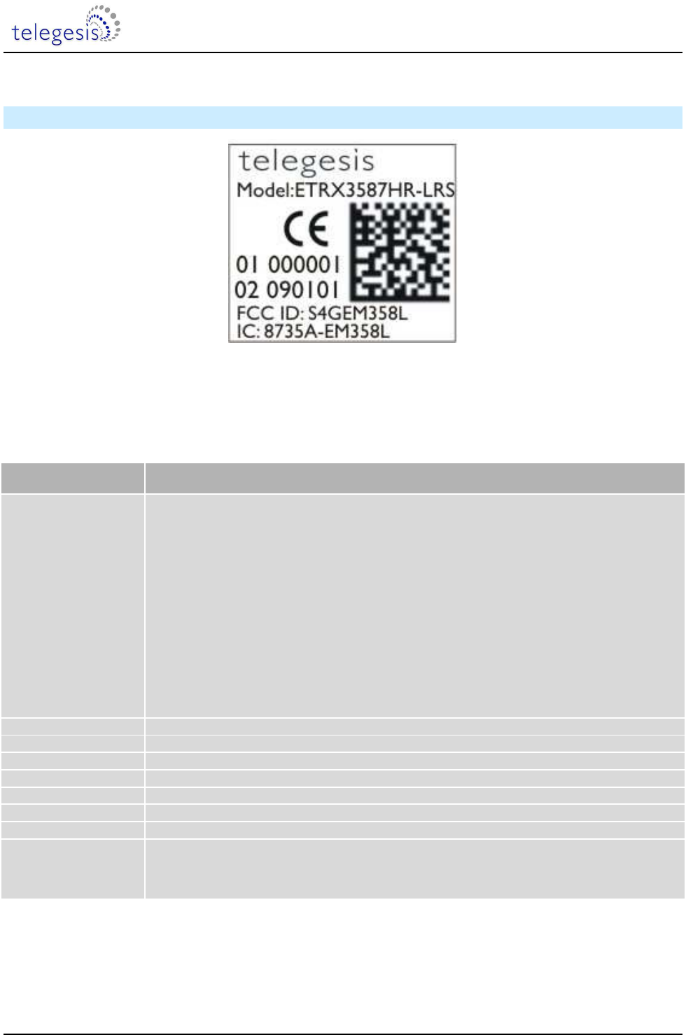
13 Product Label Drawing
Figure 9. Product Label
The label dimensions are 16mm x 14 mm. The label will withstand temperatures used during
reflow soldering. The characters “HR” are only present on the versions with the Hirose connector,
Imprint
Description
ETRX3587HR-LRS
Module Order code Possible codes are:
- ETRX3581-LRS
- ETRX3581HR-LRS
- ETRX3582-LRS
- ETRX3582HR-LRS
- ETRX3585-LRS
- ETRX3585HR-LRS
- ETRX3586-LRS
- ETRX3586HR-LRS
- ETRX3587-LRS
- ETRX3587HR-LRS
- ETRX3588-LRS
- ETRX3588HR-LRS
000001 Indication for the serial number.
090101 Production Date Code in the format YYMMDD, e.g. 090602
01 Indication for factory ID
02 Indication for the hardware revision
FCC ID: S4GEM358L FCC ID code for this product
IC: 8735A-EM358L The IC ID
CE The CE Mark
2D-Barcode
Information in the 2D-Barcode are the serial number [6 characters], the Part-Order code,
identifier for the batch number [2 characters], the identifier for the hardware release [2
characters] and the production date code in the format Year-Month-Day [6 characters], all
separated by a semicolon.
Table 19. ETRX358x-LRS Label Details
ETRX358x-LRS and ETRX358x-LRS
©2014 Telegesis (UK) Ltd - 30 - ETRX358x-LRS Product Manual
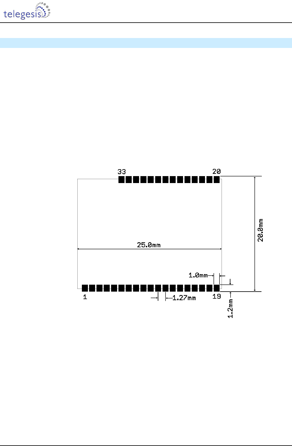
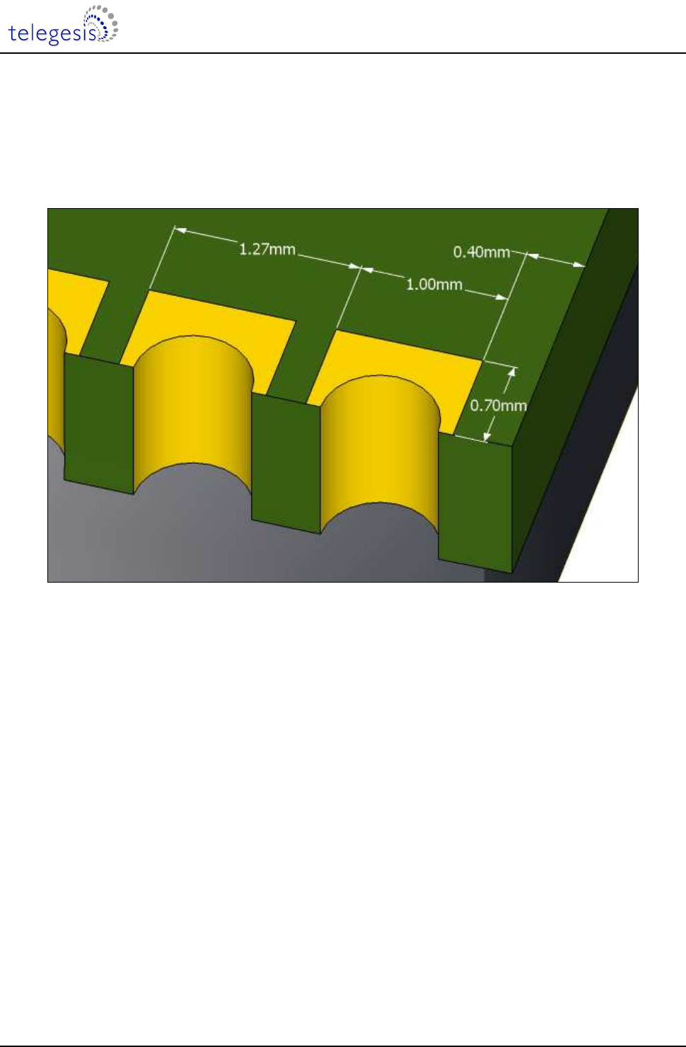
14 Recommended Footprint
In order to surface mount an ETRX3 series module, we recommend that you use pads which are
1mm wide and 1.2mm high. Unless using the “HR” variants the “keep-out” zone shown in section
11 must be retained, and it must be ensured that this area is free of copper tracks and/or copper
planes/layers.
You must also ensure that there is no exposed copper on your layout which may contact with the
underside of the ETRX3 series module.
For best RF performance it is required to provide good ground connections to the ground pads of
the module. It is recommended to use multiple vias between each ground pad and a solid ground
plane to minimize inductivity in the ground path.
Figure 10. Recommended Footprint
The land pattern dimensions above serve as a guideline.
We recommend that you use the same pad dimensions for the solder paste screen as you have for
the copper pads. However these sizes and shapes may need to be varied depending on your
soldering processes and your individual production standards. We recommend a paste screen
thickness of 120µm to 150µm.
Figure 11 shows the typical pad dimensions of the module and Figure 12-Figure 14 in section 14.1
show examples of how to align the module on its host PCB.
ETRX358x-LRS and ETRX358x-LRS
©2014 Telegesis (UK) Ltd - 31 - ETRX358x-LRS Product Manual
Although the undersides of the ETRX3 series modules are fully coated, no exposed copper, such
as through-hole vias, planes or tracks on your board component layer, should be located below the
ETRX3 series module in order to avoid ‘shorts’. All ETRX3 series modules use a multilayer PCB
containing an inner RF shielding ground plane, therefore there is no need to have an additional
copper plane directly under the ETRX3 series module.
Figure 11. Typical pad dimensions
Finally it is recommended to use no clean flux when soldering the ETRX358x family of modules
and to not use a washing process after reflow. If the process does require washing then care must
be taken that no washing agent is trapped underneath the shielding can after the drying process
has completed.
ETRX358x-LRS and ETRX358x-LRS
©2014 Telegesis (UK) Ltd - 32 - ETRX358x-LRS Product Manual
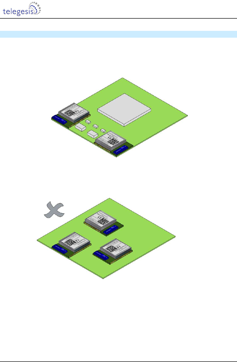
14.1 Recommended Placement
When placing the module please either locate the antenna in the corner as shown in Figure 12 so
that the recommended antenna keepout zone is being followed, or add a no copper zone as
indicated in Figure 14.
Figure 12. Typical placement
Figure 13. How to not place the Module
ETRX358x-LRS and ETRX358x-LRS
©2014 Telegesis (UK) Ltd - 33 - ETRX358x-LRS Product Manual
Figure 14. Adding a no copper / no component area
ETRX358x-LRS and ETRX358x-LRS
©2014 Telegesis (UK) Ltd - 34 - ETRX358x-LRS Product Manual
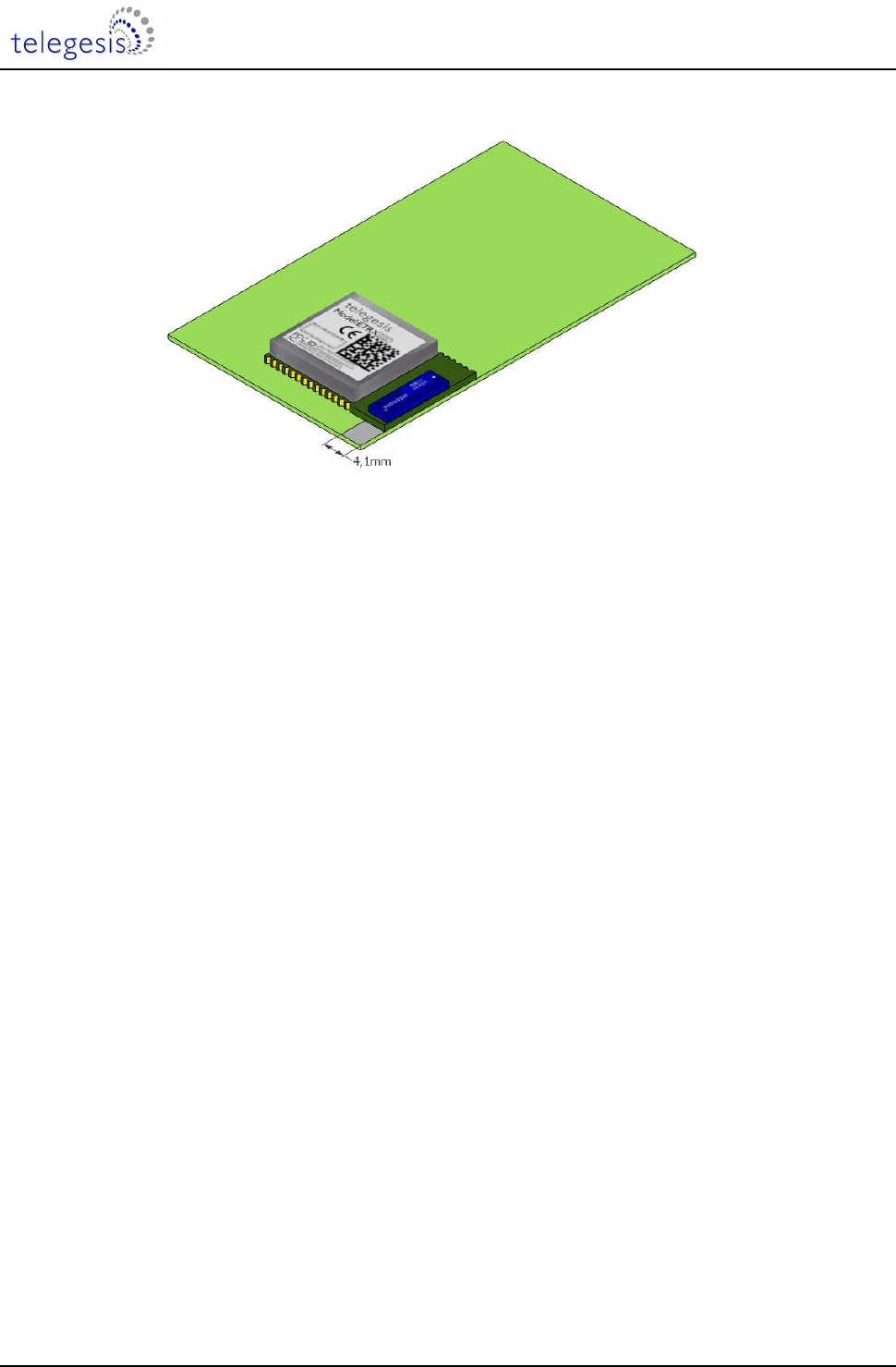
14.2 Example carrier board
Since the RF performance of the module with the on board antenna is strongly dependent on the
proper location of the module on its carrier board figure 17 shows the reference carrier board
which was used during testing by Telegesis.
Figure 17: Reference Board
For best performance it is recommended to locate the antenna towards the corner of the carrier
board and to respect the recommended keep-out areas as described in section 11.
Finally to provide a good reference ground to the on board antenna, the carrier board should have
a ground plane spanning no less than 40 x 40mm. In many cases a smaller ground plane will
suffice, but a degradation in radio performance could be the result.

ETRX358x-LRS and ETRX358x-LRS
©2014 Telegesis (UK) Ltd - 35 - ETRX358x-LRS Product Manual
15 Reliability Tests
The following measurements will be conducted after the module has been exposed to standard
room temperature and humidity for 1 hour.
No
Item
Limit
Condition
1 Vibration test Electrical parameter should be
in specification
Freq.:40Hz,Amplitude:1.5mm
20min. / cycle,1hrs. each of X and Y axis
2 Shock test the same as the above Dropped onto hard wood from height of
50cm for 10 times
3 Heat cycle test the same as the above -40°C for 30min. and +85°C for 30min.;
each temperature 300 cycles
5 Low temp. test the same as the above -40°C, 300h
6 High temp. test the same as the above +85°C, 300h
Table 20: Reliability Tests
16 Application Notes
16.1 Safety Precautions
These specifications are intended to preserve the quality assurance of products as individual
components.
Before use, check and evaluate their operation when mounted on your products. Abide by
these specifications when using the products. These products may short-circuit. If electrical
shocks, smoke, fire, and/or accidents involving human life are anticipated when a short
circuit occurs, then provide the following failsafe functions as a minimum:
(1) Ensure the safety of the whole system by installing a protection circuit and a protection
device.
(2) Ensure the safety of the whole system by installing a redundant circuit or another
system to prevent a single fault causing an unsafe status.
16.2 Design Engineering Notes
(1) Heat is the major cause of shortening the life of these products. Avoid assembly and
use of the target equipment in conditions where the product’s temperature may exceed
the maximum allowable.
(2) Failure to do so may result in degrading of the product’s functions and damage to the
product.
(3) If pulses or other transient loads (a large load applied in a short time) are applied to the
products, before use, check and evaluate their operation when assembled onto your
products.
(4) These products are not intended for other uses, other than under the special conditions
shown below. Before using these products under such special conditions, check their
performance and reliability under the said special conditions carefully, to determine
whether or not they can be used in such a manner.

ETRX358x-LRS and ETRX358x-LRS
©2014 Telegesis (UK) Ltd - 36 - ETRX358x-LRS Product Manual
(5) In liquid, such as water, salt water, oil, alkali, or organic solvent, or in places where
liquid may splash.
(6) In direct sunlight, outdoors, or in a dusty environment
(7) In an environment where condensation occurs.
(8) In an environment with a high concentration of harmful gas (e.g. salty air, HCl, Cl2,
SO2, H2S, NH3, and NOx)
(9) If an abnormal voltage is applied due to a problem occurring in other components or
circuits, replace these products with new products because they may not be able to
provide normal performance even if their electronic characteristics and appearances
appear satisfactory.
(10) Mechanical stress during assembly of the board and operation has to be avoided.
(11) Pressing on parts of the metal cover or fastening objects to the metal cover is not
permitted.
16.3 Storage Conditions
(1) The module must not be stressed mechanically during storage.
(2) Do not store these products in the following conditions or the performance
characteristics of the product, such as RF performance, may well be adversely
affected:
(3) Storage in salty air or in an environment with a high concentration of corrosive gas,
such as Cl2, H2S, NH3, SO2, or NOX
(4) Storage (before assembly of the end product) of the modules for more than one year
after the date of delivery at your company even if all the above conditions (1) to (3)
have been met, should be avoided.
ETRX358x-LRS and ETRX358x-LRS
©2014 Telegesis (UK) Ltd - 37 - ETRX358x-LRS Product Manual
17 Packaging
17.1 Embossed Tape
(1) Dimension of the tape
(2) Cover tape peel force
Force direction
Speed = 300mm/min.
Cover tape peel force
=0.098~0.68N (10~70g)
θ= 10deg
(3) Empty pockets
NB: Empty pockets in the component packed area will be less than two per reel and those empty
pockets will not be consecutive.
Empty pockets
more
Components
Empty pockets
Top cover
tape
Direction of
feed
g
ETRX358x-LRS and ETRX358x-LRS
©2014 Telegesis (UK) Ltd - 38 - ETRX358x-LRS Product Manual
17.2 Component Orientation
Top cover tape will not obstruct the carrier tape holes and will not extend beyond the edges of the
carrier tape
(top view)
Component Orientation
Part No.
Direction
17.3 Reel Dimensions
(4) Quantity per reel: 600 pieces
(5) Marking: Part No. / Quantity / Lot No. and manufacturer part# with bar-code will be on
the reel
ETRX358x-LRS and ETRX358x-LRS
©2014 Telegesis (UK) Ltd - 39 - ETRX358x-LRS Product Manual
17.4 Packaging
(6) Each reel will be packed in a hermetically-sealed bag
(7) Marking: Reel / Antistatic Packaging / Reel Box and outer Box will carry the following
label
Imprint Description
MFG P/N: 99X902DL Internal use
Lot: 00 Internal use
P/N:ETRX3587-LRS Telegesis Module Order Code.
Quantity:600 Quantity of modules inside the reel/carton
Reel No: 000001 Six digit unique Reel number counting up from 000001
Date:120824
Date Code in the format YYMMDD, e.g. 120824
P/C: ETRX3587-LRS-
R308 Module product code with reference to firmware/module type selected during ATE. If
needed multiline.
2D-Barcode
Information in the 32x32 Datamatrix 2D-Barcode are and identifier “!REEL” [5
characters], the reel number [6 characters], the Module Order code [max 18 characters
], the quantity [max 4 characters] , the date code in the format Year-Month-Day [6
characters] and the product code [max 40 characters] , all separated by a semicolon.

ETRX358x-LRS and ETRX358x-LRS
©2014 Telegesis (UK) Ltd - 40 - ETRX358x-LRS Product Manual
18 Ordering Information
2
MOQ and Lead Time applies. Only stocked modules are ETRX3587 and ETRX3587HR
Ordering/Product Code
Description
ETRX3581
-
LRS
2
ETRX3582-LRS
2
ETRX3585-LRS
2
ETRX3586-LRS
2
ETRX3587-LRS
ETRX3588-LRS
2
Power amplified Telegesis Wireless Mesh Networking Module
with Silicon Labs ZigBee Technology:
• Based on Silicon Labs EM358x SoC
• Telegesis AT Style Command Interpreter based on
• EmberZNet meshing and self-healing ZigBee PRO
stack
• Integrated 2.4GHz Antenna
ETRX3581HR
-
LRS
2
ETRX3582HR-LRS
2
ETRX3585HR-LRS
2
ETRX3586HR-LRS
2
ETRX3587HR-LRS
ETRX3588HR-LRS
2
Power amplified Telegesis Wireless Mesh Networking Module
with Silicon Labs ZigBee
Technology:
• Based on Silicon Labs EM358x SoC
• Telegesis AT Style Command Interpreter based on
• EmberZNet meshing and self-healing ZigBee PRO
stack
• U.FL coaxial Antenna Connector
ETRX357DVK
Telegesis Development Kit with:
• 3 x ETRX3DVK Development Boards
• 3 x USB cables
• 2 x ETRX357 on carrier boards
• 2 x ETRX357HR on carrier boards
• 2 x ETRX357-LRS on carrier boards
• 2 x ETRX357HR-LRS on carrier boards
• 1 x ETRX3USB USB stick
• 2 x ½-wave antennae
• 2 x ¼-wave antennae
ETRX3587 Expansion Pack
•
2 x ETRX3587 on carrier boards
• 2 x ETRX3587HR on carrier boards
• 2 x ETRX3587-LRS on carrier boards
• 2 x ETRX3587HR-LRS on carrier boards
Notes:
• Customers’ PO’s must state the Ordering/Product Code.
• There is no “blank” version of the ETRX358x modules available. All Modules are pre-
programmed with the Telegesis AT style command interpreter based on the EmberZNet
stack. (In case it is desired to program custom firmware the pre-programmed firmware can
simply be overwritten).

ETRX358x-LRS and ETRX358x-LRS
©2014 Telegesis (UK) Ltd - 41 - ETRX358x-LRS Product Manual
19 Trademarks
All trademarks, registered trademarks and products names are the sole property of their respective
owners.
20 Disclaimer
Product and company names and logos referenced may either be trademarks or registered
trademarks of their respective companies. We reserve the right to make modifications and/or
improvements without prior notification. All information is correct at time of issue. Telegesis (UK)
Ltd does not convey any license under its patent rights or assume any responsibility for the use of
the described product
21 RoHS Declaration
Declaration of environmental compatibility for supplied products:
Hereby we declare to our best present knowledge based on the declaration of our suppliers that
this product does not contain any of the substances which are banned by Directive 2011/65/EU
(RoHS)
22 Data Sheet Status
Telegesis (UK) Ltd. reserves the right to change the specification without notice, in order to
improve the design and supply the best possible product. Please consult the most recently issued
data sheet before initiating or completing a design.
23 Life Support Policy
This product is not designed for use in life support appliances, devices, or systems where
malfunction can reasonably be expected to result in a significant personal injury to the user, or as a
critical component in any life support device or system whose failure to perform can be reasonably
expected to cause the failure of the life support device or system, or to affect its safety or
effectiveness. Customers using or selling these products for use in such applications do so at their
own risk and agree to fully indemnify Telegesis (UK) Ltd. for any damages resulting.

ETRX358x-LRS and ETRX358x-LRS
©2014 Telegesis (UK) Ltd - 42 - ETRX358x-LRS Product Manual
24 Related Documents
[1] IEEE Standard 802.15.4 –2003 Wireless Medium Access Control (MAC) and Physical
Layer (PHY) Specifications for Low-Rate Wireless Personal Area Networks (LR-
WPANs)
[2] Datasheet EM35x, Ember. (www.ember.com)
[3] Datasheet U.FL-Series 2004.2 Hirose Ultra Small Surface Mount Coaxial Connectors -
Low Profile 1.9mm or 2.4mm Mated Height
[4] The ZigBee specification (www.zigbee.org)
[5] Specification for Antenova Rufa Antenna (www.antenova.com)
[6] Embedded Antenna design Ltd. (EAD Ltd.) (www.ead-ltd.com)
25 Contact Information
Website: www.telegesis.com
E-mail sales@telegesis.com
Telegesis (UK) Limited
Abbey Barn Business Centre
Abbey Barn Lane
High Wycombe
Bucks
HP10 9QQ
UK
Tel: +44 (0)1494 510199
Fax: +44 (0)5603 436999