Silicon Laboratories Finland WF111 IEEE 802.11b/g/n Wi-Fi module WF111 User Manual WF111 Datasheet

Silicon Laboratories Finland Oy IEEE 802.11b/g/n Wi-Fi module WF111 WF111 Datasheet

Contents

User Manual and Installations
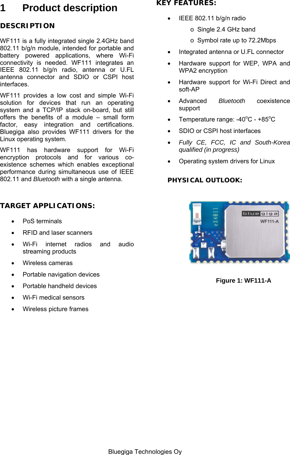
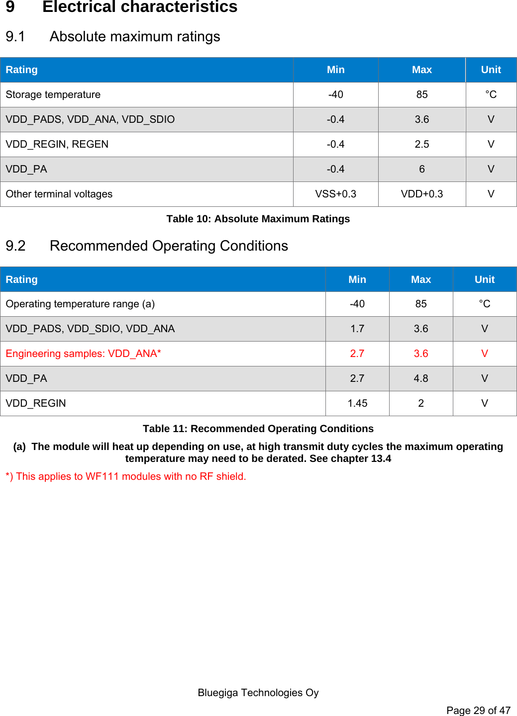
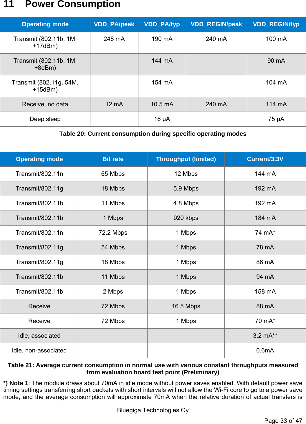
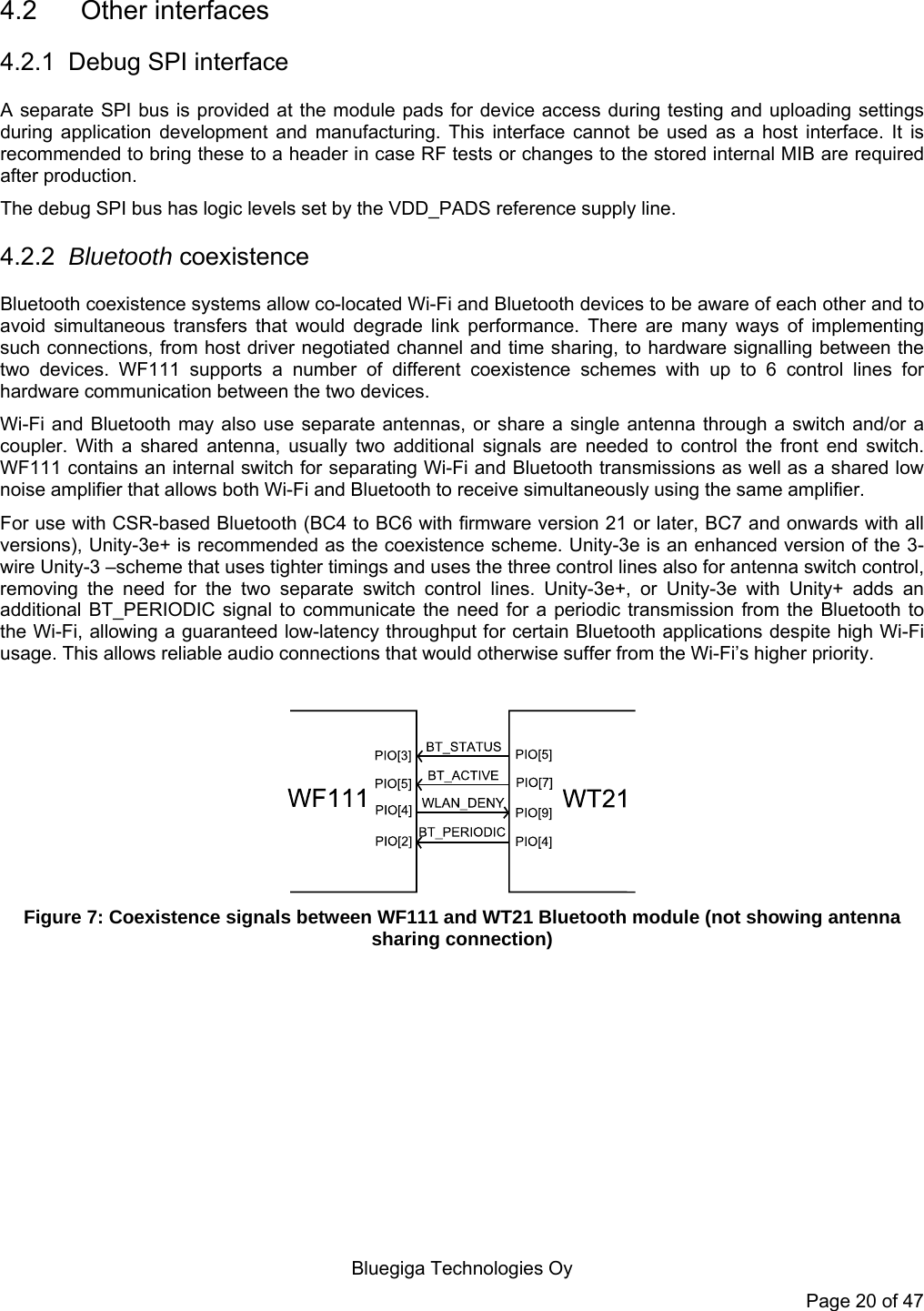
                      WF111 – 802.11 B/G/N MODULE DATA SHEET Wednesday, 11 July 2012 Version 1.1.4
  Bluegiga Technologies Oy                         Copyright © 2000-2012 Bluegiga Technologies All rights reserved.  Bluegiga Technologies assumes no responsibility for any errors which may appear in this manual.  Furthermore, Bluegiga Technologies reserves the right to alter the hardware, software, and/or specifications detailed here at any time without notice and does not make any commitment to update the information contained here. Bluegiga’s products are not authorized for use as critical components in life support devices or systems. The WRAP, Bluegiga Access Server, Access Point and iWRAP are registered trademarks of Bluegiga Technologies.  The Bluetooth trademark is owned by the Bluetooth SIG Inc., USA and is licensed to Bluegiga Technologies. All other trademarks listed herein are owned by their respective owners.
  Bluegiga Technologies Oy VERSION HISTORY Version  Comment 1.0   First public version 1.1  Product codes updated 1.1.1 Added sleep clock specifications 1.1.2  Added frequency variation table 1.1.3  FCC and IC information added 1.1.4  WT111-N layout guide
  Bluegiga Technologies Oy TABLE OF CONTENTS 1 Product description ....................................................................................................................................... 6 2 Ordering Information..................................................................................................................................... 7 3 Pinout and terminal descriptions .................................................................................................................. 8 4 Interfaces .................................................................................................................................................... 12 4.1 Host interfaces ................................................................................................................................... 12 4.1.1 Host selection ................................................................................................................................ 12 4.1.2 SDIO interface ............................................................................................................................... 12 4.1.3 CSR Serial Peripheral Interface (CSPI) ......................................................................................... 13 4.1.4 SDIO/CSPI deep-sleep control schemes ...................................................................................... 15 4.1.5 CCCR and CIS register defaults .................................................................................................... 16 4.2 Other interfaces ................................................................................................................................. 20 4.2.1 Debug SPI interface ....................................................................................................................... 20 4.2.2 Bluetooth coexistence .................................................................................................................... 20 4.2.3 Configurable I/O pads .................................................................................................................... 21 5 Clock generation ......................................................................................................................................... 22 5.1 32.768 kHz external reference clock ................................................................................................. 22 6 Power Control and Regulation ................................................................................................................... 23 6.1 Power Control and Regulation ........................................................................................................... 23 6.2 REGEN .............................................................................................................................................. 24 6.3 RESET ............................................................................................................................................... 24 7 Example Application Schematic ................................................................................................................. 26 8 Wi-Fi radio .................................................................................................................................................. 28 8.1 Wi-Fi receiver ..................................................................................................................................... 28 8.2 Wi-Fi transmitter ................................................................................................................................ 28 8.3 Antenna switch for Bluetooth coexistence ......................................................................................... 28 9 Electrical characteristics ............................................................................................................................. 29 9.1 Absolute maximum ratings ................................................................................................................ 29 9.2 Recommended Operating Conditions ............................................................................................... 29 9.3 Input/Output terminal characteristics ................................................................................................. 30 10 RF Characteristics ................................................................................................................................. 31 11 Power Consumption .............................................................................................................................. 33 12 Physical Dimensions .............................................................................................................................. 35 13 Layout Guidelines .................................................................................................................................. 36 13.1 WF111-A ............................................................................................................................................ 36 13.2 WF111-E ............................................................................................................................................ 36 13.3 WF111-N ............................................................................................................................................ 36 13.4 Thermal considerations ..................................................................................................................... 38
  Bluegiga Technologies Oy 13.5 EMC considerations ........................................................................................................................... 38 14 Soldering Recommendations................................................................................................................. 40 15 Certifications .......................................................................................................................................... 41 15.1 Wi-Fi ................................................................................................................................................... 41 15.2 CE ...................................................................................................................................................... 41 15.3 FCC and IC ........................................................................................................................................ 41 15.3.1 FCC et IC ................................................................................................................................... 43 15.4 Qualified Antenna Types for WF111-E .............................................................................................. 46 Contact Information ........................................................................................................................................... 47
  Bluegiga Technologies Oy 1 Product description DESCRIPTION WF111 is a fully integrated single 2.4GHz band 802.11 b/g/n module, intended for portable and battery powered applications, where Wi-Fi connectivity is needed. WF111 integrates an IEEE 802.11 b/g/n radio, antenna or U.FL antenna connector and SDIO or CSPI host interfaces. WF111 provides a low cost and simple Wi-Fi solution for devices that run an operating system and a TCP/IP stack on-board, but still offers the benefits of a module – small form factor, easy integration and certifications. Bluegiga also provides WF111 drivers for the Linux operating system. WF111 has hardware support for Wi-Fi encryption protocols and for various co-existence schemes which enables exceptional performance during simultaneous use of IEEE 802.11 and Bluetooth with a single antenna.  TARGET APPLICATIONS:  PoS terminals   RFID and laser scanners  Wi-Fi internet radios and audio streaming products  Wireless cameras   Portable navigation devices   Portable handheld devices   Wi-Fi medical sensors   Wireless picture frames                   KEY FEATURES:   IEEE 802.11 b/g/n radio o  Single 2.4 GHz band o  Symbol rate up to 72.2Mbps    Integrated antenna or U.FL connector   Hardware support for WEP, WPA and WPA2 encryption   Hardware support for Wi-Fi Direct and soft-AP  Advanced  Bluetooth coexistence support  Temperature range: -40oC - +85oC   SDIO or CSPI host interfaces  Fully CE, FCC, IC and South-Korea qualified (in progress)   Operating system drivers for Linux  PHYSICAL OUTLOOK:   Figure 1: WF111-A
  Bluegiga Technologies Oy Page 7 of 47 2 Ordering Information WF1 1 1- X           Antenna:A = Internal antennaE = ExternalN = RF pinWF111 Product Numbering  Confirmed products and codes Product code  Description WF111-A  WF111 module with internal chip antenna WF111-E  WF111 module with U.FL connector for external antenna WF111-N  WF111 module with 50 RF pin (contact sales@bluegiga.com for availability) DKWF111  WF111-A SDIO evaluation kit
  Bluegiga Technologies Oy Page 8 of 47 3  Pinout and terminal descriptions 20PIO[3]19VDD_PADS18PIO[4]17VDD_REGIN16PIO[2]15VDD_SDIO21GND22PIO[0]23REGEN24PIO[1]25RST26SPI_CS27PIO[5]28VDD_PA29GND14 GND13 SPI_MOSI12 SPI_CLK11 SPI_MISO10 VDD_ANA9BT8GND7SDIO_CMD6SDIO_CLK5SDIO_DAT[3]4SDIO_DAT[2]3SDIO_DAT[1]2SDIO_DAT[0]1GND33 GND_PAD30 GND31 ANT32 GND Figure 2: WF111 pinout
  Bluegiga Technologies Oy Page 9 of 47  POWER SUPPLIES  PIN NUMBER  DESCRIPTION VDD_REGIN  17  Input for the internal regulators REGEN  23  Pull high to enable internal voltage regulators (2.0V max) GND  1, 8, 14, 21, 29, 30, 32  Ground GND_PAD  33  Thermal pad, on bottom of WF111 VDD_ANA  10  Positive supply for PA control VDD_PADS  19  Positive supply for the digital interfaces VDD_SDIO  15  Positive supply for the SDIO interface VDD_PA  28  Positive supply for the power amplifier Table 1: Supply Terminal Descriptions  PIO PORT  PIN NUMBER  PAD TYPE  DESCRIPTION PIO[0]  22 Bi-directional, programmable strength internal pull-down/pull-up Programmable input/output line.   Can be used for Bluetooth co-existence. PIO[1]  24 PIO[2]  16 PIO[3]  20 PIO[4]  18 PIO[5]  27 Table 2: GPIO Terminal Descriptions
  Bluegiga Technologies Oy Page 10 of 47  SDIO/CSPI Interfaces  PIN NUMBER  PAD TYPE  DESCRIPTION SDIO_DATA[0] 2 Bi-directional, tri-state, weak internal pull-up  Synchronous data input/output SDIO_SPI_DI  SDIO SPI data output CSPI_MISO  CSPI data output SDIO_DATA[1] 3 Synchronous data input/output SDIO_SPI_INT  SDIO SPI interrupt output CSPI_INT  CSPI data input SDIO_DATA[2]  4  Synchronous data input/output SDIO_DATA[3] 5  Bi-directional, weak/strong internal pull-up Synchronous data input/output SDIO_SPI_CS#  SDIO SPI chip select, active low CSPI_CS#  CSPI chip select, active low SDIO_CLK 6  Input, weak internal pull-up SDIO clock SDIO_SPI_SCLK  SDIO SPI clock CSPI_CLK  CSPI clock SDIO_CMD 7  Bi-directional, weak internal pull-up SDIO data input SDIO_SPI_MOSI  SDIO SPI data input CSPI_MOSI  CSPI data input Table 3: Host Interface Terminal Descriptions
  Bluegiga Technologies Oy Page 11 of 47  OTHER SIGNALS  PIN NUMBER  PAD TYPE  DESCRIPTION RST  25  Input, weak internal pull-up, active low  System reset ANT  31  RF, DC blocked  Antenna output on N variant, on A and E variants not connected BT  9  RF, DC blocked  Bluetooth antenna sharing RF input Table 4: Other Terminal Descriptions   DEBUG SPI INTERFACE  PIN NUMBER  PAD TYPE  DESCRIPTION SPI_MISO  11  Output, tri-state, weak internal pull-down  Synchronous data output SPI_CLK  12  Input, weak internal pull-down Synchronous clock input SPI_MOSI  13  Synchronous data input SPI_CS  26  Debug SPI Chip select, active low Table 5: Debug SPI Terminal Descriptions
  Bluegiga Technologies Oy Page 12 of 47 4 Interfaces 4.1 Host interfaces WF111 can be interfaced by the host using SDIO in 1bit or 4bit mode, SDIO SPI or CSR proprietary CSPI connection. The host connection buses can be clocked up to 50MHz. 4.1.1 Host selection WF111 will default to 1-bit SDIO mode. The host interface can be set with 1-bit SDIO or SDIO SPI commands to the required mode. After mode selection, it will then remain in that mode until the module is reset either with the RESET pin or the internal power supply supervisor. 4.1.2 SDIO interface This is a host interface which allows a Secure Digital Input Output (SDIO) host to gain access to the internals of the chip. All defined slave modes (SPI, SD 1bit, SD 4bit) are provided.  Two functions are supported:   Function 0 is mandatory function used for SDIO slave configuration. This contains CCCR, FBR and CIS. CCCR registers support sleep and wakeup signaling.   Function 1 provides access to the IEEE 802.11 functionality. Command IO_RW_DIRECT (CMD52) is used to directly access internal registers. IO_RW_EXTENDED (CMD53) is used for block transfer to/from module MMU buffers.  Command  SD Mode (1/4 bit)  SDIO SPI Mode GO_IDLE_STATE (CMD0)  Y  Y SEND_RELATIVE_ADDR (CMD3)  Y  N IO_SEND_OP_COND (CMD5)  Y  Y SELECT/DESELECT_CARD (CMD7)  Y  N GO_INACTIVE_STATE (CMD15)  Y  N IO_RW_DIRECT (CMD52)  Y  Y IO_RW_EXTENDED (CMD53)  Y  Y CRC_ON_OFF (CMD59)  N  Y Table 6: Supported commands per mode For more information and detailed descriptions of above functions and commands, see the following specifications:  SD Specifications Part 1 Physical Layer Specification v.1.10  SD Specification Part E1 SDIO Specification v.1.10
  Bluegiga Technologies Oy Page 13 of 47 4.1.3  CSR Serial Peripheral Interface (CSPI) The CSPI is a host interface which shares pins with the SDIO. It contains a number of modifications on the SDIO SPI specification aimed at increasing the host bus efficiency in hosts supporting SPI but not SDIO. The main advantages compared to SDIO SPI are:   Burst transfer is continuous instead of blocks with CRC   Timings are deterministic (fixed number of clocks) reducing the required interaction   16 bit registers are transferred as a single command instead of two 8 bit writes MMU buffers are accessed using burst read/writes. The command and address fields are used to select the correct buffer. The CSPI is able to generate an interrupt to the host when a memory access fails. This interrupt line is shared with the SDIO functions. The CSPI Interface is an extension of the basic SPI Interface, with the access type determined by the following fields:  8-bit command  24-bit address   16-bit burst length (optional). Only applicable for burst transfers into or out of the MMU 4.1.3.1  CSPI read/write cycles Register read/write cycles are used to access Function 0, Bluetooth acceleration and MCU registers. Burst read/write cycles are used to access the MMU. 4.1.3.2 CSPI register write cycle The command and address are locked into the slave, followed by 16bits of write data. An Error Byte is returned on the MISO signal indicating whether or not the transfer has been successful.  Figure 3: CSPI Register Write Cycle 4.1.3.3 CSPI register read cycle The command and address field are clocked into the slave, the slave then returns the following:   Bytes of padding data (MISO held low)  Error byte   16-bits of read data  Figure 4: CSPI Register Read Cycle
  Bluegiga Technologies Oy Page 14 of 47 4.1.3.4 CSPI register burst write cycle Burst transfers are used to access the MMU buffers. They cannot be used to access registers. Burst read/write cycles are selected by setting the nRegister/Burst bit in the command field to 1. Burst transfers are byte orientated, have a minimum length of 0 bytes and a maximum length of 64kbytes. Setting the length field to 0 results in no data being transferred to or from the MMU. As with a register access, the command and address fields are transferred first. There is an optional length field transferred after the address. The use of the length field is controlled by the LengthFieldPresent bit in the Function 0 registers, which is cleared on reset.  Figure 5: CSPI Burst Write Cycle 4.1.3.5 CSPI register read cycle Burst reads have a programmable amount of padding data that is returned by the slave. 0-15 bytes are returned as defined in the BurstPadding register. Following this the Error byte is returned followed by the data. Once the transfer has started, no further padding is needed. A FIFO within SDIO_TOP will pre-fetch the data. The address is not retransmitted, and is auto-updated within the slave. The length field is transmitted if LengthFieldPresent in the Function 0 registers is set. In the absence of a length field the CSB signal is used to indicate the end of the burst.  Figure 6: CSPI Burst Read Cycle
  Bluegiga Technologies Oy Page 15 of 47  4.1.4  SDIO/CSPI deep-sleep control schemes The module automatically enters deep sleep to minimize power consumption after a while of idling. Deep sleep is the lowest power mode, where the processor, the internal reference (fast) clock, and much of the digital and analogue hardware are shut down. The SDIO communication system however remains on, and is clocked by the host system. During deep sleep only the function 0 is available, while attempts to access Function 1 will likely result in bus timeouts.  Control of when the module is allowed to enter deep sleep is done via Vendor Unique Register in CCCR in function 0. Wake-up is also initiated through this register. The module will initiate an SDIO interrupt when the wake-up is complete.
  Bluegiga Technologies Oy Page 16 of 47 4.1.5  CCCR and CIS register defaults  AddressBitsFieldnameValue0x00  3-0  CCRx: CCCR format version number 0x2(a); CCCR/FBR version 1.20 7-4  SDIOx: SDIO spec. version 0x3(a); SDIO 2.00 0x01  3-0  SDx: SD format version number  0x1; SD Physical Specification 1.10 0x07  6  SCSI: Support continuous SPI interrupt supported 0x1 0x08  0  SDC: Card supports direct commands during data transfer 0x1; IO_RW_DIRECT can be executed while transfer in progress 1  SMB: Card supports multiblock  0x1; IO_RW_EXTENDED can be executed in block mode 2  SRW: Card supports read wait  0x1; Wait signal is supported on SDIO_DAT[2] 3  SBS: Card supports suspend/resume  0x0; Operations can't be suspended 4  S4MI: Supports interrupt between data blocks in 4-bit SD 0x0; Block interrupts not supported in 4-bit multi-block transfer 6  LSC: Card is a low-speed card  0x0; Full-speed card 7  4BLS: 4-bit support for low-speed cards  0x0; Full-speed card 0x09-0x0B  23-0  Pointer to card's common CIS  0x001000; Pointer to the start of Card Information Structure 0x12  0  SMPC: Support master power control  0x1; Total card current may exceed 200mA (EMPC, SPS and EPS are available) 0x13  0  SHS: Support high-speed  0x1(a); High speed mode supported (enabled by the host via the EHS bit) Table 7: SDIO CCCR values, (a) can be modified by software
  Bluegiga Technologies Oy Page 17 of 47  AddressBitsFieldnameValue0x100  3-0  Standard SDIO Function interface code  0x0; No SDIO standard interface supported by this function (no defined interface for IEEE 802.11 6  Supports CSA  0x0; No Code Storage Area 0x101  7-0  Extended Standard SDIO Function interface 0x00; No SDIO standard interface supported by this function 0x102  0  SPS  0x1; This function has two power modes which are selected by EPS 0x109-0x10B  23-0  Pointer to standard Function 1 CIS  0x002000; Pointer to the start of the CIS for this function Table 8: SDIO FBR values for Function 1  AddressFieldnameValue0x00 TPL_CODE 0x21; CISTPL_FUNCID: Function identification tuple 0x01  TPL_LINK  0x02; Link to next tuple 0x02  TPLFID_FUNCTION  0x0C; Card function tuple 0x03 TPFLID_SYSINIT  0x00; System init bit mask (not used) 0x04 TPL_CODE 0x22; CISTPL_FUNCE: Function extension tuple 0x05  TPL_LINK  0x05; Link to next tuple 0x06  TPLFE_TYPE  0x00; Type of extended data = Function 0 0x07-0x08 TPLFE_FN0_BLK_SIZE 0x0200; Maximum block size and byte count = 512 0x09 TPLFE_MAX_TRAN_SPEED 0x5A(a); Maximum transfer speed per line = 50 Mbps 0x0A TPL_CODE  0x20; CISTPL_MANDIF: Manufacturer identification string tuple 0x0B  TPL_LINK  0x04; Link to next tuple 0x0C-0x0D TPLMID_MAND_CODE  0x032A(a); Card manufacturer code = CSR 0x0E-0x0F TPLMID_CARD  0x0007(a); Manufacturer information - UniFi CSR6031 0x10  TPL_CODE  0xFF; End-of-chain tuple Table 9: SDIO CIS values for Function 0, (a) can be modified by software
  Bluegiga Technologies Oy Page 18 of 47 AddressFieldnameValue0x00 TPL_CODE 0x21; CISTPL_FUNCID: Function identification tuple 0x01  TPL_LINK  0x02; Link to next tuple 0x02  TPLFID_FUNCTION  0x0C; Card function tuple 0x03 TPFLID_SYSINIT  0x00; System init bit mask (not used) 0x04 TPL_CODE 0x22; CISTPL_FUNCE: Function extension tuple 0x05  TPL_LINK  0x05; Link to next tuple 0x06  TPLFE_TYPE  0x00; Type of extended data = Function 1-7 0x07  TPLFE_FUNCTION_INFO  0x01(a); FNWUS: Wake up support = 1 (card can wake up host with SDIO clock stopped) 0x08  TPLFE_STD_IO_REV  0x00; No SDIO standard function supported 0x09-0x0C  TPL_CARD_PSN  0x00000000(a); Product serial number 0x0D-0x10  TPLFE_CSA_SIZE  0x00000000; No code storage area 0x11 TPLFE_CSA_PROPERTY  0x00; No code storage area 0x12-0x13 TPLFE_MAX_BLOCK_SIZE 0x0200; Maximum block size and byte count = 5120x14-0x17 TPLFE_OCR 0x00FF8000(a); 2.7-3.6V operation supported 0x18 TPLFE_OP_MIN_PWR 0x14(a); Minimum operating current = 20mA 0x19 TPLFE_OP_AVG_PWR 0x32(a); Average operating current = 50mA 0x1A TPLFE_OP_MAX_PWR 0xC8(a); Maximum operating current = 500mA 0x1B TPLFE_SB_MIN_PWR 0x05(a); Minimum current in standby = 5mA 0x1C TPLFE_SB_AVG_PWR 0x07(a); Average current in standby = 7mA 0x1D  TPLFE_SB_MAX_PWR  0x0A(a); Maximum current in standby = 10mA 0x1E-0x1F  TPLFE_MIN_BW  0x0BB8(a); Minimum data transfer bandwidth = 3000kBps (24Mbps) 0x20-0x21 TPLFE_OPT_BW 0x1B58(a); Optimum data transfer bandwidth = 7000kBps (54Mbps) 0x22-0x23 TPLFE_ENABLE_TIMEOUT_VAL 0x001F4; Function's timeout after being enabled = 5s 0x24-0x25 TPLFE_SP_AVG_PWR_3.3V 0x0032(a); Average current when operating = 50mA (copy of TPLFE_OP_AVG_PWR) 0x26-0x27 TPLFE_SP_MAX_PWR_3.3V 0x00C8(a); Maximum current when operating = 200mA (copy of TPLFE_OP_MAX_PWR) 0x28-0x29 TPLFE_HP_AVG_PWR_3.3V 0x00C8(a); Average current when operating in higher current mode = 200mA 0x2A-0x2B TPLFE_HP_MAX_PWR_3.3V 0x015E(a); Maximum current when operating in higher current mode = 350mA 0x2C-0x2D TPLFE_LP_AVG_PWR_3.3V  0x078(a); Average current when operating in lower current mode = 120mA 0x2E-0x2F TPLFE_LP_MAX_PWR_3.3V 0x00C8(a); Maximum current when operating in lower current mode = 200mA
  Bluegiga Technologies Oy Page 19 of 47 0x30 TPL_CODE  0xFF; CISTPL_END: End-of-chain tuple  Table 11: SDIO CIS values for Function 1, (a) can be modified by software; current consumption figures are conservative values for the host power control
  Bluegiga Technologies Oy Page 20 of 47 4.2 Other interfaces 4.2.1  Debug SPI interface A separate SPI bus is provided at the module pads for device access during testing and uploading settings during application development and manufacturing. This interface cannot be used as a host interface. It is recommended to bring these to a header in case RF tests or changes to the stored internal MIB are required after production. The debug SPI bus has logic levels set by the VDD_PADS reference supply line. 4.2.2  Bluetooth coexistence Bluetooth coexistence systems allow co-located Wi-Fi and Bluetooth devices to be aware of each other and to avoid simultaneous transfers that would degrade link performance. There are many ways of implementing such connections, from host driver negotiated channel and time sharing, to hardware signalling between the two devices. WF111 supports a number of different coexistence schemes with up to 6 control lines for hardware communication between the two devices. Wi-Fi and Bluetooth may also use separate antennas, or share a single antenna through a switch and/or a coupler. With a shared antenna, usually two additional signals are needed to control the front end switch. WF111 contains an internal switch for separating Wi-Fi and Bluetooth transmissions as well as a shared low noise amplifier that allows both Wi-Fi and Bluetooth to receive simultaneously using the same amplifier. For use with CSR-based Bluetooth (BC4 to BC6 with firmware version 21 or later, BC7 and onwards with all versions), Unity-3e+ is recommended as the coexistence scheme. Unity-3e is an enhanced version of the 3-wire Unity-3 –scheme that uses tighter timings and uses the three control lines also for antenna switch control, removing the need for the two separate switch control lines. Unity-3e+, or Unity-3e with Unity+ adds an additional BT_PERIODIC signal to communicate the need for a periodic transmission from the Bluetooth to the Wi-Fi, allowing a guaranteed low-latency throughput for certain Bluetooth applications despite high Wi-Fi usage. This allows reliable audio connections that would otherwise suffer from the Wi-Fi’s higher priority.   Figure 7: Coexistence signals between WF111 and WT21 Bluetooth module (not showing antenna sharing connection)
  Bluegiga Technologies Oy Page 21 of 47 The required MIB values for the coexistence scheme in Figure 7 are:  unifiCoexScheme ::= 3  unifiCoexPTABTStatusPIO ::= 3  unifiCoexPTABTInbandPIO ::= -1  unifiCoexPTABTActivePIO ::= 5  unifiCoexPTAWLANDenyPIO ::= 4 unifiCoexPeriodicPIO ::= 2  The corresponding PSKEYs for the WT21 are:  PSKEY_LC_COMBO_DISABLE_PIO_MASK (0x0028) = 0x0200 0x0000 0x0000 PSKEY_LC_COMBO_DOT11_CHANNEL_PIO_BASE (0x002A) = 0x0011 PSKEY_LC_COMBO_DOT11_ESCO_RTX_PRIORITY ( 0x0050) = 0x0001 PSKEY_LC_COMBO_DOT11_PULL_DISABLE_MASK (0x005A) = 0x0200 PSKEY_LC_COMBO_DOT11_PERIODIC_PIO_MASK (0x005C) = 0x0010 0x0000 PSKEY_LC_COMBO_DOT11_T1 (0x005E) = 0x0043 PSKEY_LC_COMBO_DOT11_T2 (0x005F) = 0x000A PSKEY_TXRX_PIO_CONTROL (0x0209) = 0x0001  For other coexistence schemes, please contact Bluegiga technical support. 4.2.3  Configurable I/O pads A number of programmable bi-directional input/outputs (I/O) are provided. PIO[0:5] logic levels are referred to the VDD_PADS supply line. PIO lines can be configured through software to implement various automated functions or as generic inputs or outputs. As inputs the lines can be configured to have either weak or strong pull-ups or pull-downs. All PIO lines are configured as inputs with weak pull-downs at reset. In addition to the coexistence functions, any of the PIO lines can be configured as interrupt request lines, wake-up lines from sleep modes, status led drivers with multiple internally generated modes, general I/O pins controlled by the host, or as a 32.768 kHz sleep clock input.  For further information, please contact Bluegiga technical support. Note: All unused signals can be left floating.
  Bluegiga Technologies Oy Page 22 of 47 5 Clock generation WF111 uses an internal 26 MHz crystal as the RF reference clock. All WF111 internal digital clocks except sleep timing are generated using phase locked loops, which are locked to the 26 MHz reference clock.  5.1  32.768 kHz external reference clock The module contains an integrated RC oscillator for sleep timing. If more accurate timing is required, an external 32.768 kHz clock can be applied to a PIO pin configured as a clock input to implement a more accurate sleep clock. The Wi-Fi packet timing is derived from the 26MHz crystal and so is unaffected by tolerances in the sleep clock. The pin chosen as a clock input is an ordinary digital input and the clock waveform should be a logic level square wave. Configuring an input as a clock input requires a setting in the MIB.  For further information, please contact Bluegiga technical support.
  Bluegiga Technologies Oy Page 23 of 47 6  Power Control and Regulation 6.1  Power Control and Regulation  Figure 8: System block diagram WF111 contains four linear regulators supplying clean voltages for the different parts of the system. All of them produce a 1.2V output voltage, and are fed from a common input, VDD_REGIN. This input can be supplied with a voltage between 1.45-2.0V, typically 1.5V or 1.8V. The VDD_REGIN supply should be relatively clean of ripple and switching spikes in order to avoid degrading the RF performance.   WF111 also needs four other supply lines connected in addition to VDD_REGIN:    VDD_PADS provides a reference voltage for matching voltage levels of the host system to the GPIO pins used for Bluetooth coexistence and other functions. This can range from 1.7V to 3.6V. The current drawn from this supply is negligible.   VDD_SDIO provides a reference voltage for matching voltage levels of the host system to the SDIO connection. This can range from 1.7V to 3.6V. The current drawn from this supply depends on bus usage, but with no active data transfer will be negligible.   VDD_ANA provides a reference voltage for communication between the Wi-Fi chip and the power amplifier. This should be between 1.7V and 3.6V. The current drawn from this supply is negligible.   Note for WF111 engineering sample version without RF shield: o VDD_ANA provides a reference voltage for communication between the Wi-Fi chip and the power amplifier. This should be between 2.7V and 3.6V. The current drawn from this supply is negligible. In the production version, the voltage range for VDD_ANA has been extended for more flexible supplying.   VDD_PA is a separate supply voltage for the Wi-Fi power amplifier. This supply will draw considerable currents in pulses and should be bypassed with a relatively large capacitor close to the module, and the power traces should be relatively wide. This voltage can range from 2.7V to 4.8V making use
  Bluegiga Technologies Oy Page 24 of 47 directly from a single lithium cell possible. A higher supply voltage will not affect the power amplifiers current draw significantly. These voltages are not tied to each other and any combination of supply voltages within the specified limits can be used. In a 3.3V logic level host system all other supplies would usually be tied to the 3.3V supply, with a separate regulator providing the 1.45-2.0V supply for the Wi-Fi core. A switch mode regulator with 1.5V output is recommended for minimum power consumption. Please see the example schematic in this datasheet. In a 1.8V logic level host system, all other supplies can be connected to the 1.8V supply rail except VDD_PA which should be connected to a 2.7-4.8V supply. Note for WF111 engineering sample version without RF shield: In a 1.8V logic level host system VDD_PA would be connected to a 2.7-4.8V supply, VDD_ANA to a 2.7-3.6V supply and the rest of the supplies to the 1.8V supply rail. The higher voltage supplies should be powered before or at the same time as the core supply line, i.e. the VDD_REGIN should be powered up last. Powering the core first may lead to the GPIO and SDIO blocks booting into an inaccessible state.  External high frequency bypassing of the supply lines is not required. Note: All supply voltages and ground lines must be connected. 6.2 REGEN The regulator enable pin REGEN is used to enable the WF111. REGEN enables the regulators of the digital and analog core supply voltages. The pin is active high, with a logic threshold of around 1V, and has a weak pull-down. REGEN can tolerate voltages up to 2.0V, and may be connected directly to the internal voltage regulator input (VDD_REGIN) to permanently enable the device. Part of the regulators can also be disabled by firmware in power saving modes. The VDD_REGIN supply can also be externally switched off while leaving the other supply voltages powered. Cutting power to the core will fully shut down the module internal processors and returning power will cause a power-on reset, requiring a full initialization of the module. The REGEN pin will not disable system blocks not supplied by the core supply, meaning the coexistence interface and the SDIO Function 0 are available even when the core is powered off.  6.3 RESET WF111 may be reset from several sources: RESET pin, power-on reset, via software configured watchdog timers as well as through the SDIO/CSPI host interface. The RESET pin is an active low reset and is internally filtered using the internal low frequency clock oscillator. A reset is performed between 1.5 and 4.0ms following RESET being active. It is recommended that RESET be applied for a period greater than 5ms. The power-on reset occurs when the core supply (generated by the internal 1.2V linear regulator) falls below typically 1.05V and is released when core voltage rises above typically 1.10V. At reset regardless of the source the digital I/O pins are set to a high impedance state with weak pull-downs, except RESET and DEBUG_SPI_CS# which have a weak pull-up. The host connection interface is only reset by the RESET pin or a power-on reset. A power-on reset can be achieved through powering down the digital core by either externally cutting the VDD_REGIN supply or giving a low pulse to the REGEN-pad. If REGEN is connected to the host system for powering down the module, or a separate core power switch is implemented, the RESET pin can be tied permanently to a supply voltage line.
  Bluegiga Technologies Oy Page 25 of 47 Following a reset, WF111 automatically generates internally the clocks needed for safe boot-up of the internal processors. The crystal oscillator is then configured by software with the correct input frequency.
  Bluegiga Technologies Oy Page 26 of 47 7 Example Application Schematic SDIO bus3.3V1.5/1.8Vregulator20PIO[3]19VDD_PADS18PIO[4]17VDD_REGIN16PIO[2]15VDD_SDIO21GND22PIO[0]23REGEN24PIO[1]25RST26SPI_CS27PIO[5]28VDD_PA29GND14 GND13 SPI_MOSI12 SPI_CLK11 SPI_MISO10 VDD_ANA9BT8GND7SDIO_CMD6SDIO_CLK5SDIO_DAT[3]4SDIO_DAT[2]3SDIO_DAT[1]2SDIO_DAT[0]1GND33 GND_PAD30 GND31 ANT32 GND100uF3VIN 2VOUT1GNDCMDCLKDAT[3]DAT[2]DAT[1]DAT[0]RESET+3.3V Figure 9: An example application circuit with SDIO host connection, 3.3V level host logic and 1.5/1.8V core supply, REGEN hard wired to the core supply and RST pad used to reset the module (Note: with N-variant ANT-pad and associated grounds would also be connected)
  Bluegiga Technologies Oy Page 27 of 47 SDIO bus20PIO[3]19VDD_PADS18PIO[4]17VDD_REGIN16PIO[2]15VDD_SDIO21GND22PIO[0]23REGEN24PIO[1]25RST26SPI_CS27PIO[5]28VDD_PA29GND14 GND13 SPI_MOSI12 SPI_CLK11 SPI_MISO10 VDD_ANA9BT8GND7SDIO_CMD6SDIO_CLK5SDIO_DAT[3]4SDIO_DAT[2]3SDIO_DAT[1]2SDIO_DAT[0]1GND33 GND_PAD30 GND31 ANT32 GND100uFCMDCLKDAT[3]DAT[2]DAT[1]DAT[0]+1.8V2.7-4.8VREGEN Figure 10: An example application circuit with SDIO host connection, 1.8V level host logic and a separate power amplifier supply, RST hard wired to the core supply and REGEN pad used to power off and reset the module (Note: with N-variant ANT-pad and associated grounds would also be connected)(Note: engineering samples will require VDD_ANA to be 2.7-3.6V)
  Bluegiga Technologies Oy Page 28 of 47 8 Wi-Fi radio 8.1 Wi-Fi receiver The receiver features direct conversion architecture. Sufficient out-of-band blocking specification at the Low Noise Amplifier (LNA) input allows the receiver to be used in close proximity to Global System for Mobile Communications (GSM) and Wideband Code Division Multiple Access (W-CDMA) cellular phone transmitters without being desensitized. High-order baseband filters ensure good performance against in-band interference. 8.2 Wi-Fi transmitter The transmitter features a direct IQ modulator. Digital baseband transmit circuitry provides the required spectral shaping and on-chip trims are used to reduce IQ modulator distortion. Transmitter gain can be controlled on a per-packet basis, allowing the optimization of the transmit power as a function of modulation scheme. The internal Power Amplifier (PA) has a maximum output power of +15dBm for IEEE 802.11g/n and +17dBm for IEEE 802.11b. The module internally compensates for PA gain and reference oscillator frequency drifts with varying temperature and supply voltage. 8.3 Antenna switch for Bluetooth coexistence WF111 supports sharing the integrated antenna or antenna connector with a Bluetooth device through the BT_RF pad. The module contains a bypass switch to route the Bluetooth signal directly to the antenna, and supports using the internal LNA for Bluetooth reception. The switch is controlled through the coexistence interface.
  Bluegiga Technologies Oy Page 29 of 47 9 Electrical characteristics 9.1 Absolute maximum ratings Rating  Min  Max  Unit Storage temperature  -40  85  °C VDD_PADS, VDD_ANA, VDD_SDIO  -0.4  3.6  V VDD_REGIN, REGEN  -0.4  2.5  V VDD_PA  -0.4  6  V Other terminal voltages  VSS+0.3  VDD+0.3  V Table 10: Absolute Maximum Ratings 9.2 Recommended Operating Conditions Rating  Min  Max  Unit Operating temperature range (a)  -40  85  °C VDD_PADS, VDD_SDIO, VDD_ANA  1.7  3.6  V Engineering samples: VDD_ANA*  2.7  3.6  V VDD_PA  2.7  4.8  V VDD_REGIN  1.45  2  V Table 11: Recommended Operating Conditions (a)  The module will heat up depending on use, at high transmit duty cycles the maximum operating temperature may need to be derated. See chapter 13.4 *) This applies to WF111 modules with no RF shield.
  Bluegiga Technologies Oy Page 30 of 47  9.3  Input/Output terminal characteristics Digital Terminals  Min  Typ  Max  Unit Input Voltage Levels VIL input logic level low 1.7V ≤ VDD ≤ 3.6V  -0.3  -  0.25*Vdd  V VIH input logic level low 1.7V ≤ VDD ≤ 3.6V  0.625*Vdd  -  VDD+0.3  V Output Voltage Levels VOL output logic level low 1.7V ≤ VDD ≤ 3.6V,  (Io = 4.0 mA)  -  -  0.4  V VOH output logic level low 1.7V ≤ VDD ≤ 3.6V,  (Io = -4.0 mA)  0.75*Vdd  -  Vdd  V Input Tri-state Current with: Strong pull-up  -150  -40  -10  µA Strong pull-down  10  40  150  µA Weak pull-up  -5  -1  -0.33  µA Weak pull-down  0.33  1  5  µA I/O pad leakage current  -1  0  1  µA Pad input capacitance  1  -  5  pF Table 12: Digital terminal electrical characteristics   Min  Typ  max   Frequency  32.748  32.768  32.788  kHz Deviation @25oC  -20   +20  ppm Deviation over temperature  -150   +150  ppm Duty cycle  30  50  70  % Rise time      50  ns Input high level  0.625Vdd    Vdd+0.3  V Input low level  -0.3   0.25Vdd  V Table 13: External sleep clock specifications
  Bluegiga Technologies Oy Page 31 of 47  10 RF Characteristics  Min  max   Channel  1  13 Note: channel 14 can be set but proper operation is not guaranteed and its use should be avoided. Frequency  2412  2472  MHz Table 14: Supported frequencies  Standard  Supported bit rates 802.11b  1, 2, 5.5, 11Mbps 802.11g  6, 9, 12, 18, 24, 36, 48, 54Mbps 802.11n, HT, 20MHz, 800ns  6.5, 13, 19.5, 26, 39, 52, 58.5, 65Mbps 802.11n, HT, 20MHz, 400ns  7.2, 14.4, 21.7, 28.9, 43.3, 57.8, 65, 72.2Mbps Table 15: Supported modulations  802.11b  Typ  802.11g  Typ  802.11n short GI  Typ  802.11n long GI  Typ 1 Mbps  -97 dBm  6 Mbps  -92 dBm  6.5 Mbps  -91 dBm  7.2 Mbps  -92 dBm 2 Mbps  -95 dBm  9 Mbps  -91 dBm  13 Mbps  -87 dBm  14.4 Mbps  -90 dBm 5.5 Mbps  -93 dBm  12 Mbps  -89 dBm  19.5 Mbps  -85 dBm  21.7 Mbps  -87 dBm 11 Mbps  -89 dBm  18 Mbps  -87 dBm  26 Mbps  -82 dBm  28.9 Mbps  -84 dBm     24 Mbps  -84 dBm  39 Mbps  -78 dBm  43.3 Mbps  -80 dBm     36 Mbps  -80 dBm  52 Mbps  -74 dBm  57.8 Mbps  -75 dBm     48 Mbps  -75 dBm  58.5 Mbps  -71 dBm  65 Mbps  -72 dBm     54 Mbps  -73 dBm  65 Mbps  -68 dBm  72.2 Mbps  -69 dBm Table 16: Receiver sensitivity
  Bluegiga Technologies Oy Page 32 of 47 Modulation type  Min  Typ  Max   802.11b  +16  +17  +17.6  dBm802.11g  +14  +15  +15.6  dBm802.11n  +14  +15  +15.6  dBmTable 17: Transmitter output power at maximum setting  Operating mode  Min  Typ  Max   TX loss  -2.5  -3  -3.5  dB RX gain (using internal LNA)  8  10  12  dB Internal LNA noise figure   2.0  2.5  dB Table 18: BT antenna sharing interface properties   Typ  Max  802.11 limit (total error)   Variation between individual units  +/-5  +/-10  +/-25  ppm Variation with temperature  +/-3  +/-10  +/-25  ppm Table 19: Carrier frequency accuracy
  Bluegiga Technologies Oy Page 33 of 47 11 Power Consumption Operating mode  VDD_PA/peak  VDD_PA/typ  VDD_REGIN/peak  VDD_REGIN/typ Transmit (802.11b, 1M, +17dBm) 248 mA  190 mA  240 mA  100 mA Transmit (802.11b, 1M, +8dBm)  144 mA   90 mA Transmit (802.11g, 54M, +15dBm)  154 mA   104 mA Receive, no data  12 mA  10.5 mA  240 mA  114 mA Deep sleep   16 µA   75 µA Table 20: Current consumption during specific operating modes  Operating mode  Bit rate  Throughput (limited)  Current/3.3V Transmit/802.11n  65 Mbps  12 Mbps  144 mA Transmit/802.11g  18 Mbps  5.9 Mbps  192 mA Transmit/802.11b  11 Mbps  4.8 Mbps  192 mA Transmit/802.11b  1 Mbps  920 kbps  184 mA Transmit/802.11n  72.2 Mbps  1 Mbps  74 mA* Transmit/802.11g  54 Mbps  1 Mbps  78 mA Transmit/802.11g  18 Mbps  1 Mbps  86 mA Transmit/802.11b  11 Mbps  1 Mbps  94 mA Transmit/802.11b  2 Mbps  1 Mbps  158 mA Receive  72 Mbps  16.5 Mbps  88 mA Receive  72 Mbps  1 Mbps  70 mA* Idle, associated      3.2 mA** Idle, non-associated      0.6mA Table 21: Average current consumption in normal use with various constant throughputs measured from evaluation board test point (Preliminary) *) Note 1: The module draws about 70mA in idle mode without power saves enabled. With default power save timing settings transferring short packets with short intervals will not allow the Wi-Fi core to go to a power save mode, and the average consumption will approximate 70mA when the relative duration of actual transfers is
  Bluegiga Technologies Oy Page 34 of 47 minimal. However, when longer packets are transferred with longer intervals, the Wi-Fi core will be able to sleep during the interval, reducing power consumption considerably. **) Note 2: Idle current when associated varies considerably, with 1mA to 8mA measured with different access points in a noisy office environment.
  Bluegiga Technologies Oy Page 35 of 47  12 Physical Dimensions  Figure 11: Physical dimensions  Figure 12: WF111 recommended PCB land pattern
  Bluegiga Technologies Oy Page 36 of 47 13 Layout Guidelines 13.1  WF111-A     Figure 13: Recommended layouts, on board corner and on board edge   See figure 13: recommended layout for the suggested module layout. The impedance matching of the antenna is designed for a layout similar to the module evaluation board. For an optimal performance of the antenna the layout should strictly follow the layout example shown in figure 8 and the thickness of FR4 should be between 1 and 2 mm, preferably 1.6mm.  Any dielectric material close to the antenna will change the resonant frequency and it is recommended not to place a plastic case or any other dielectric closer than 5 mm from the antenna.  ANY metal in close proximity of the antenna will prevent the antenna from radiating freely. It is recommended not to place any metal or other conductive objects closer than 20 mm to the antenna except in the directions of the ground planes of the module itself.  For optimal performance, place the antenna end of the module outside any metal surfaces and objects in the application, preferably on the device corner. The larger the angle in which no metallic object obstructs the antenna radiation, the better the antenna will work. DO NOT place WF111-A in the middle of the application board. Even with a board cutout around the antenna the range will be bad. The three pads on the antenna end of the WF111-A can be connected to the ground or left unsoldered. 13.2 WF111-E RF output can be taken directly from the U.FL connector of the module, and no antenna clearances need to be made for the module. The three pads on the antenna end of the module can be connected to the ground or left unsoldered.  13.3 WF111-N Antenna connection is routed to pad 31. Pads 30 and 32 beside the antenna connection should be properly connected to the ground plane. No antenna clearances are needed for the module itself. The antenna trace should be properly impedance controlled and kept short. Figure 14 shows a typical 50 ohm trace from the RF pin to a SMA connector.
  Bluegiga Technologies Oy Page 37 of 47  Figure 14: Typical 50 trace for WF111-N  A transmission line impedance calculator, such as TX-Line made by AWR, can be used to approximate the dimensions for the 50 ohm transmission line. Figure 15 shows an example for two different 50 ohm transmission lines. FR4, εr= 4.6Prepreg, εr= 3.7W = 0.15 mmh = 0.076 mmG = 0.25 mmGND stitching viasRF GROUNDRF GROUND RF GROUNDRF GROUNDFR4, εr= 4.6h = 1 mmW = 1.8 mmMICROSTRIPCPW Ground Figure 15: Example cross section of two different 50 ohm transmission line
  Bluegiga Technologies Oy Page 38 of 47   13.4 Thermal considerations The WF111 module may at continuous full power transmit consume up to 1 W of DC power, most of which is drawn by the power amplifier. Most of this will be dissipated as heat. In any application where high ambient temperatures and constant transmissions for more than a few seconds can occur, it is important that a sufficient cooling surface is provided to dissipate the heat.  The thermal pad in the bottom of the module must be connected to the application board ground planes by soldering. The application board should provide a number of vias under and around the pad to conduct the produced heat to the board ground planes, and preferably to a copper surface on the other side of the board in order to dissipate the heat into air. The module internal thermal resistance should in most cases be negligible compared to the thermal resistance from the module into air, and common equations for surface area required for cooling can be used to estimate the temperature rise of the module. Only copper planes on the circuit board surfaces with a solid thermal connection to the module ground pad will dissipate heat. For an application with high transmit duty cycles (low bit rate, high throughput, long bursts or constant streaming) the maximum allowed ambient temperature should be reduced due to inherent heating of the module, especially with small fully plastic enclosed applications where heat transfer to ambient air is low due to low thermal conductivity of plastic.  The module measured on the evaluation board exhibits a temperature rise of about 25oC above ambient temperature when continuously transmitting IEEE 802.11b at full power with minimal off-times and no collision detection (a worst case scenario regarding power dissipation). An insufficiently cooled module will rapidly heat beyond operating range in ambient room temperature. 13.5 EMC considerations Following recommendations helps to avoid EMC problems arising in the design. Note that each design is unique and the following list do not consider all basic design rules such as avoiding capacitive coupling between signal lines. Following list is aimed to avoid EMC problems caused by RF part of the module.    Do not remove copper from the PCB more than needed. For proper operation the antenna requires a solid ground plane with as much surface area as possible. Use ground filling as much as possible. Connect all grounds together with multiple vias. Do not leave small floating unconnected copper areas or areas connected by just one via, these will act as additional antennas and raise the risk of unwanted radiations.   Do not place a ground plane underneath the antenna. The grounding areas under the module should be designed as shown in Figure 13: Recommended layout.   When using overlapping ground areas use conductive vias separated max. 3 mm apart at the edge of the ground areas. This prevents RF from penetrating inside the PCB. Use ground vias extensively all over the PCB. All the traces in (and on) the PCB are potential antennas. Especially board edges should have grounds connected together at short intervals (stitching) to avoid resonances.   Avoid current loops. Keep the traces with sensitive, high current or fast signals short, and mind the return current path, having a short signal path is not much use if the associated ground path between the ends of the signal trace is long. Remember, ground is also a signal trace. The ground will conduct the same current as the signal path and at the same frequency, power and sensitivity.    Split a ground plane ONLY if you know exactly what you are doing. Splitting the plane may cause more harm than good if applied incorrectly. The ground plane acts as a part of the antenna system. Insufficient ground planes or large separate sensitive signal ground planes will easily cause the coupled transmitted pulses to be AM-demodulated by semiconductor junctions around the board, degrading system performance.
  Bluegiga Technologies Oy Page 39 of 47 Overlapping GND layers without GND stitching viasOverlapping GND layers with GND stitching vias shielding the RF energy Figure 16: Use of stitching vias to avoid emissions from the edges of the PCB
  Bluegiga Technologies Oy Page 40 of 47 14 Soldering Recommendations WF111 is compatible with industrial standard reflow profile for Pb-free solders. The reflow profile used is dependent on the thermal mass of the entire populated PCB, heat transfer efficiency of the oven and particular type of solder paste used. Consult the datasheet of particular solder paste for profile configurations.  Bluegiga Technologies will give following recommendations for soldering the module to ensure reliable solder joint and operation of the module after soldering. Since the profile used is process and layout dependent, the optimum profile should be studied case by case. Thus following recommendation should be taken as a starting point guide.  -  Refer to technical documentations of particular solder paste for reflow profile configurations -  Avoid using more than one flow.  -  Reliability of the solder joint and self-alignment of the component are dependent on the solder volume. Minimum of 150m stencil thickness is recommended.  -  Aperture size of the stencil should be 1:1 with the pad size.  -  A low residue, “no clean” solder paste should be used due to low mounted height of the component. -  If the vias used on the application board have a diameter larger than 0.3mm, it is recommended to mask the via holes at the module side to prevent solder wicking through the via holes. Solders have a habit of filling holes and leaving voids in the thermal pad solder junction, as well as forming solder balls on the other side of the application board which can in some cases be problematic.
  Bluegiga Technologies Oy Page 41 of 47 15 Certifications WF111 is compliant to the following specifications: 15.1 Wi-Fi TBD 15.2 CE TBD 15.3 FCC and IC This device complies with Part 15 of the FCC Rules. Operation is subject to the following two conditions:  (1) this device may not cause harmful interference, and  (2) this device must accept any interference received, including interference that may cause undesired operation.  FCC RF Radiation Exposure Statement:  This equipment complies with FCC radiation exposure limits set forth for an uncontrolled environment. End users must follow the specific operating instructions for satisfying RF exposure compliance. This transmitter must not be co-located or operating in conjunction with any other antenna or transmitter. This transmitter is considered as mobile device and should not be used closer than 20 cm from a human body. To allow portable use in a known host class 2 permissive change is required. Please contact support@bluegiga.com for detailed information.    IC Statements:  This device complies with Industry Canada license-exempt RSS standard(s). Operation is subject to the following two conditions: (1) this device may not cause interference, and (2) this device must accept any interference, including interference that may cause undesired operation of the device. Under Industry Canada regulations, this radio transmitter may only operate using an antenna of a type and maximum (or lesser) gain approved for the transmitter by Industry Canada. To reduce potential radio interference to other users, the antenna type and its gain should be so chosen that the equivalent isotropically radiated power (e.i.r.p.) is not more than that necessary for successful communication.  If detachable antennas are used: This radio transmitter (identify the device by certification number, or model number if Category II) has been approved by Industry Canada to operate with the antenna types listed below with the maximum permissible gain and required antenna impedance for each antenna type indicated. Antenna types not included in this list, having a gain greater than the maximum gain indicated for that type, are strictly prohibited for use with this device. See table 22 for the approved antennas for WF111-E and WF111-N.
  Bluegiga Technologies Oy Page 42 of 47 OEM Responsibilities to comply with FCC and Industry Canada Regulations The WF111 Module has been certified for integration into products only by OEM integrators under the following conditions:    The antenna(s) must be installed such that a minimum separation distance of 20cm is maintained between the radiator (antenna) and all persons at all times.   The transmitter module must not be co-located or operating in conjunction with any other antenna or transmitter.  As long as the two conditions above are met, further transmitter testing will not be required. However, the OEM integrator is still responsible for testing their end-product for any additional compliance requirements required with this module installed (for example, digital device emissions, PC peripheral requirements, etc.).  IMPORTANT NOTE: In the event that these conditions cannot be met (for certain configurations or co-location with another transmitter), then the FCC and Industry Canada authorizations are no longer considered valid and the FCC ID and IC Certification Number cannot be used on the final product. In these circumstances, the OEM integrator will be responsible for re-evaluating the end product (including the transmitter) and obtaining a separate FCC and Industry Canada authorization.  End Product Labeling The WF111 Module is labeled with its own FCC ID and IC Certification Number. If the FCC ID and IC Certification Number are not visible when the module is installed inside another device, then the outside of the device into which the module is installed must also display a label referring to the enclosed module.  In that case, the final end product must be labeled in a visible area with the following:   “Contains Transmitter Module FCC ID: QOQWF111” “Contains Transmitter Module IC: 5123A-BGTWF111” or  “Contains FCC ID: QOQWF111 “Contains IC: 5123A-BGTWF111”   The OEM of the WF111 Module must only use the approved antenna(s) described in table 22, which have been certified with this module.  The OEM integrator has to be aware not to provide information to the end user regarding how to install or remove this RF module or change RF related parameters in the user manual of the end product.  To comply with FCC and Industry Canada RF radiation exposure limits for general population, the antenna(s) used for this transmitter must be installed such that a minimum separation distance of 20cm is maintained between the radiator (antenna) and all persons at all times and must not be co-located or operating in conjunction with any other antenna or transmitter.
  Bluegiga Technologies Oy Page 43 of 47 15.3.1  FCC et IC Cet appareil est conforme à l’alinéa 15 des règles de la FCC. Deux conditions sont à respecter lors de son utilisation : (1) cet appareil ne doit pas créer d’interférence susceptible de causer un quelconque dommage et, (2) cet appareil doit accepter toute interférence, quelle qu’elle soit, y compris les interférences susceptibles d’entraîner un fonctionnement non requis.  Déclaration de conformité FCC d’exposition aux radiofréquences (RF): Ce matériel respecte les limites d’exposition aux radiofréquences fixées par la FCC dans un environnement non contrôlé. Les utilisateurs finaux doivent se conformer aux instructions d’utilisation spécifiées afin de satisfaire aux normes d’exposition en matière de radiofréquence. Ce transmetteur ne doit pas être installé ni utilisé en concomitance avec une autre antenne ou un autre transmetteur. Ce transmetteur est assimilé à un appareil mobile et ne doit pas être utilisé à moins de 20 cm du corps humain. Afin de permettre un usage mobile dans le cadre d’un matériel de catégorie 2, il est nécessaire de procéder à quelques adaptations. Pour des informations détaillées, veuillez contacter le support technique Bluegiga : support@bluegiga.com.  Déclaration de conformité IC : Ce matériel respecte les standards RSS exempt de licence d’Industrie Canada. Son utilisation est soumise aux deux conditions suivantes : (1) l’appareil ne doit causer aucune interférence, et (2) l’appareil doit accepter toute interférence, quelle qu’elle soit, y compris les interférences susceptibles d’entraîner un fonctionnement non requis de l’appareil. Selon la réglementation d’Industrie Canada, ce radio-transmetteur ne peut utiliser qu’un seul type d’antenne et ne doit pas dépasser la limite de gain autorisée par Industrie Canada pour les transmetteurs. Afin de réduire les interférences potentielles avec d’autres utilisateurs, le type d’antenne et son gain devront être définis de telle façon que la puissance isotrope rayonnante équivalente (EIRP) soit juste suffisante pour permettre une bonne communication.  Lors de l’utilisation d’antennes amovibles : Ce radio-transmetteur (identifié par un numéro certifié ou un numéro de modèle dans le cas de la catégorie II) a été approuvé par Industrie Canada pour fonctionner avec les antennes référencées ci-dessous dans la limite de gain acceptable et l’impédance requise pour chaque type d’antenne cité. Les antennes non référencées possédant un gain supérieur au gain maximum autorisé pour le type d’antenne auquel elles
  Bluegiga Technologies Oy Page 44 of 47 appartiennent sont strictement interdites d’utilisation avec ce matériel. Veuillez vous référer au tableau 22 concernant les antennes approuvées pour les WF111.  Les responsabilités de l’intégrateur afin de satisfaire aux réglementations de la FCC et d’Industrie Canada : Les modules WF111 ont été certifiés pour entrer dans la fabrication de produits exclusivement réalisés par des intégrateurs dans les conditions suivantes :  L’antenne (ou les antennes) doit être installée de façon à maintenir à tout instant une distance minimum de 20cm entre la source de radiation (l’antenne) et toute personne physique.  Le module transmetteur ne doit pas être installé ou utilisé en concomitance avec une autre antenne ou un autre transmetteur. Tant que ces deux conditions sont réunies, il n’est pas nécessaire de procéder à des tests supplémentaires sur le transmetteur. Cependant, l’intégrateur est responsable des tests effectués sur le produit final afin de se mettre en conformité avec d’éventuelles exigences complémentaires lorsque le module est installé (exemple : émissions provenant d’appareils numériques, exigences vis-à-vis de périphériques informatiques, etc.) ;  IMPORTANT : Dans le cas où ces conditions ne peuvent être satisfaites (pour certaines configurations ou installation avec un autre transmetteur), les autorisations fournies par la FCC et Industrie Canada ne sont plus valables et les numéros d’identification de la FCC et de certification d’Industrie Canada ne peuvent servir pour le produit final. Dans ces circonstances, il incombera à l’intégrateur de faire réévaluer le produit final (comprenant le transmetteur) et d’obtenir une autorisation séparée de la part de la FCC et d’Industrie Canada. Etiquetage du produit final  Chaque module WF111 possède sa propre identification FCC et son propre numéro de certification IC. Si l’identification FCC et le numéro de certification IC ne sont pas visibles lorsqu’un module est installé à l’intérieur d’un autre appareil, alors l’appareil en question devra lui aussi présenter une étiquette faisant référence au module inclus. Dans ce cas, le produit final doit comporter une étiquette placée de façon visible affichant les mentions suivantes :  « Contient un module transmetteur certifié FCC QOQWF111 » « Contient un module transmetteur certifié IC 5123A-BGTWF111 » ou « Inclut la certification FCC QOQWF111 »
  Bluegiga Technologies Oy Page 45 of 47 « Inclut la certification IC 5123A-BGTWF111 »  L’intégrateur du module WF111 ne doit utiliser que les antennes répertoriées dans le tableau 25 certifiées pour ce module.  L’intégrateur est tenu de ne fournir aucune information à l’utilisateur final autorisant ce dernier à installer ou retirer le module RF, ou bien changer les paramètres RF du module, dans le manuel d’utilisation du produit final.  Afin de se conformer aux limites de radiation imposées par la FCC et Industry Canada, l’antenne (ou les antennes) utilisée pour ce transmetteur doit être installée de telle sorte à maintenir une distance minimum de 20cm à tout instant entre la source de radiation (l’antenne) et les personnes physiques. En outre, cette antenne ne devra en aucun cas être installée ou utilisée en concomitance avec une autre antenne ou un autre transmetteur.
  Bluegiga Technologies Oy Page 46 of 47 15.4  Qualified Antenna Types for WF111-E This device has been designed to operate with the antennas listed below, and having a maximum gain of 2.14 dBi. Antennas not included in this list or having a gain greater than 2.14 dBi are strictly prohibited for use with this device. The required antenna impedance is 50 ohms.  Qualified Antenna Types for WF111-E Antenna Type  Maximum Gain Dipole 2.14 dBi Table 22: Qualified Antenna Types for WF111-E  Any antenna that is of the same type and of equal or less directional gain as listed in table above can be used without a need for retesting. To reduce potential radio interference to other users, the antenna type and its gain should be so chosen that the equivalent isotropically radiated power (e.i.r.p.) is not more than that permitted for successful communication. Using an antenna of a different type or gain more than 2.14 dBi will require additional testing for FCC, CE and IC. Please, contact support@bluegiga.com for more information.
  Bluegiga Technologies Oy Page 47 of 47 Contact Information Sales:   sales@bluegiga.com  Technical support: support@bluegiga.com http://techforum.bluegiga.com  Orders:   orders@bluegiga.com  WWW:   www.bluegiga.com   www.bluegiga.hk Head Office / Finland: Phone: +358-9-4355 060 Fax: +358-9-4355 0660 Sinikalliontie 5A 02630 ESPOO FINLAND Postal address / Finland: P.O. BOX 120 02631 ESPOO FINLAND Sales Office / USA: Phone: +1 770 291 2181  Fax: +1 770 291 2183 Bluegiga Technologies, Inc. 3235 Satellite Boulevard, Building 400, Suite 300 Duluth, GA, 30096, USA Sales Office / Hong-Kong: Phone: +852 3182 7321  Fax: +852 3972 5777 Bluegiga Technologies, Inc. 19/F Silver Fortune Plaza, 1 Wellington Street,  Central Hong Kong

Navigation menu