Silicon Laboratories Finland WT11E Bluetooth Module User Manual WT11 E Data Sheet
Silicon Laboratories Finland Oy Bluetooth Module WT11 E Data Sheet
UserManual.wiki
>
Silicon Laboratories Finland
>
WT11E User Manual
user manual
Navigation menu
Upload a User Manual
Namespaces
Wiki Guide
HTML
PDF
Info
Views
User Manual
Discussion / Help
Navigation
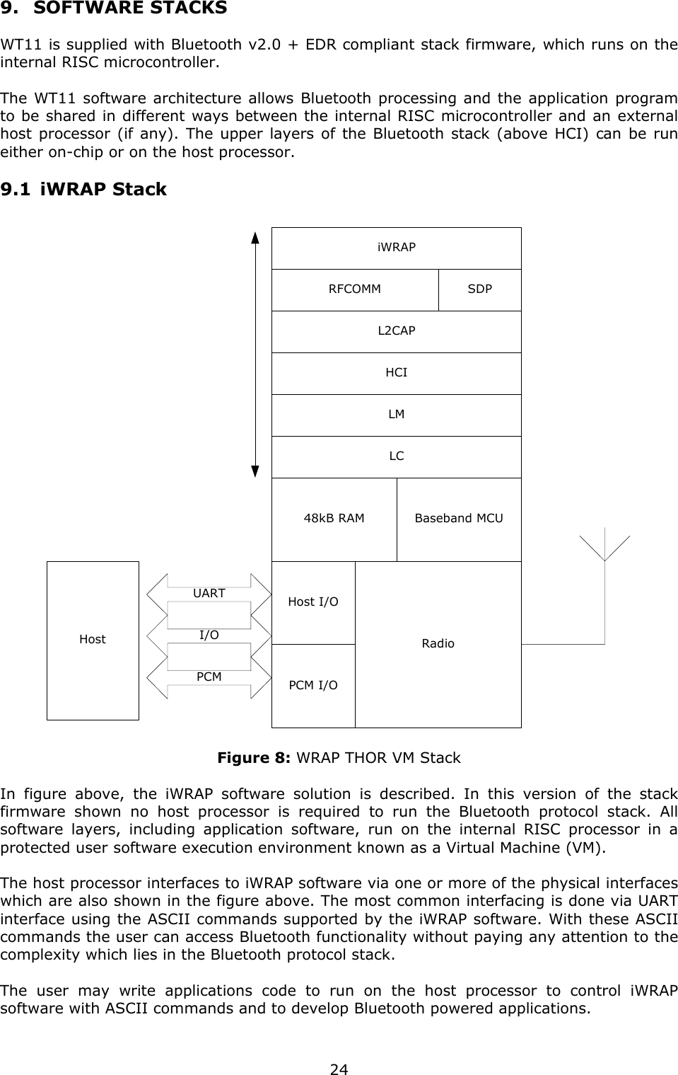
![23consists of six programmable, bi-directional I/O lines, PIO[2:7]. Programmable I/O lines can be accessed either via an embedded application running on WT11 or via private channel or manufacturer-specific HCI commands. All PIO lines are configured as inputs with weak pull downs at reset. PIO[2] / USB_PULL_UP (1) This is a multifunction terminal. The function depends on whether WT11 is a USB or UART capable version. On UART versions, this terminal is a programmable I/O. On USB versions, it can drive a pull-up resistor on USB_D+. For application using external RAM this terminal may be programmed for chip select. PIO[3] / USB_WAKE_UP (1) This is a multifunction terminal. On UART versions of WT11 this terminal is a programmable I/O. On USB versions, its function is selected by setting the Persistent Store Key PSKEY_USB_PIO_WAKEUP (0x2cf) either as a programmable I/O or as a USB_WAKE_UP function. PIO[4] / USB_ON (1) This is a multifunction terminal. On UART versions of WT11 this terminal is a programmable I/O. On USB versions, the USB_ON function is also selectable. PIO[5] / USB_DETACH (1) This is a multifunction terminal. On UART versions of WT11 this terminal is a programmable I/O. On USB versions, the USB_DETACH function is also selectable. PIO[6] / CLK_REQ This is multifunction terminal, its function is determined by Persistent Store Keys. Using PSKEY_CLOCK_REQUEST_ENABLE, (0x246) this terminal can be configured to be low when WT11 is in deep sleep and high when a clock is required. The clock must be supplied within 4ms of the rising edge of PIO[6] to avoid losing timing accuracy in certain Bluetooth operating modes. PIO[7] Programmable I/O terminal. 8. RESET The RESET pin is an active high reset and is internally filtered using the internal low frequency clock oscillator. A reset will be performed between 1.5 and 4.0ms following RESET being active. It is recommended that RESET be applied for a period greater than 5ms.](https://usermanual.wiki/Silicon-Laboratories-Finland/WT11E/User-Guide-698674-Page-24.png)
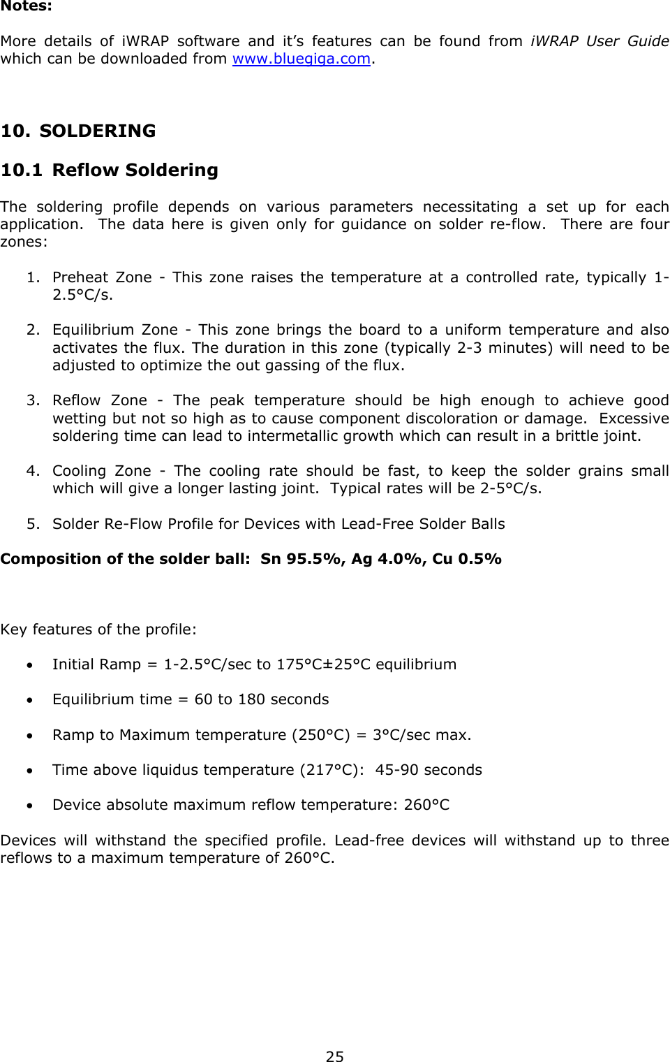
![26Certifications WT11 is compliant to the following specifications 10.2 Bluetooth The WT11-E module is Bluetooth qualified and listed as an end product. If not modified in any way, it is a complete Bluetooth entity, containing software and hardware functionality as well as the whole RF-part including the antenna. This practically translates to that if the module is used without modification of any kind, it does not need any Bluetooth approval work. If changes are made in the parameter set, added profiles or in the antenna design, it is required to be submitted to a BQB (Bluetooth Qualification Body) for evaluation on what needs to be tested. With HCI firmware WT11 will not meet the requirements of end product qualification. WT11 is Bluetooth compliant to the following specifications 1. RF as defined in Part A of the Bluetooth specification v2.0+EDR, Vol.2 Core System Package [Controller volume] (Class 1 operation) with all optional and mandatory features supported. 2. BB as defined in Part B of the Bluetooth specification v2.0+EDR, Vol.2 Core System Package [Controller volume], and specified in the covered functionality of the Software Integrated Component (Bluetooth ID: B01294) 3. LM as defined in Part C of the Bluetooth specification v2.0+EDR, Vol.2 Core System Package [Controller volume], and specified in the covered functionality of the Software Integrated Component (Bluetooth ID: B01294) 4. L2CAP as defined in Part A of the Bluetooth specification v2.0+EDR, Vol.3 Core System Package [Controller volume], and specified in the covered functionality of the Software Integrated Component (Bluetooth ID: B00477) 5. SDP as defined in Part B of the Bluetooth specification v2.0+EDR, Vol.3 Core System Package [Controller volume], and specified in the covered functionality of the Software Integrated Component (Bluetooth ID: B00477) 6. RFCOMM as defined in PART F:1 of the Bluetooth Core Specification v1.1 and specified in the covered functionality of the Software Integrated Component (Bluetooth ID: B00047). 7. Generic Access GAP as defined in PART C of the Bluetooth Core Specification v2.0+EDR, Vol.3 Core Systems Package [Host Volume], and specified in the covered functionality of the Software Integrated Component (Bluetooth ID: B00047). 8. Serial Port Profile (SPP) as defined in PART K:5 of the Bluetooth Profile Specification v1.1, and specified in the covered functionality of the Software Integrated Component (Bluetooth ID: B00047). Bluetooth identifier: B03005](https://usermanual.wiki/Silicon-Laboratories-Finland/WT11E/User-Guide-698674-Page-27.png)