Silicon Laboratories Finland WT12 Bluetooth Module User Manual WT12 Data Sheet v1 9
Silicon Laboratories Finland Oy Bluetooth Module WT12 Data Sheet v1 9
UserManual.wiki
>
Silicon Laboratories Finland
>
WT12 User Manual
Users Manual
Navigation menu
Upload a User Manual
Namespaces
Wiki Guide
HTML
PDF
Info
Views
User Manual
Discussion / Help
Navigation
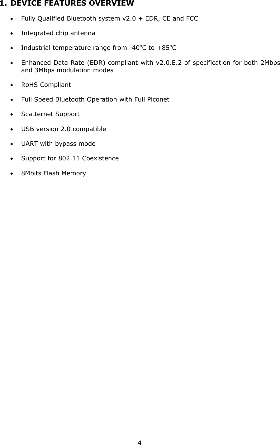
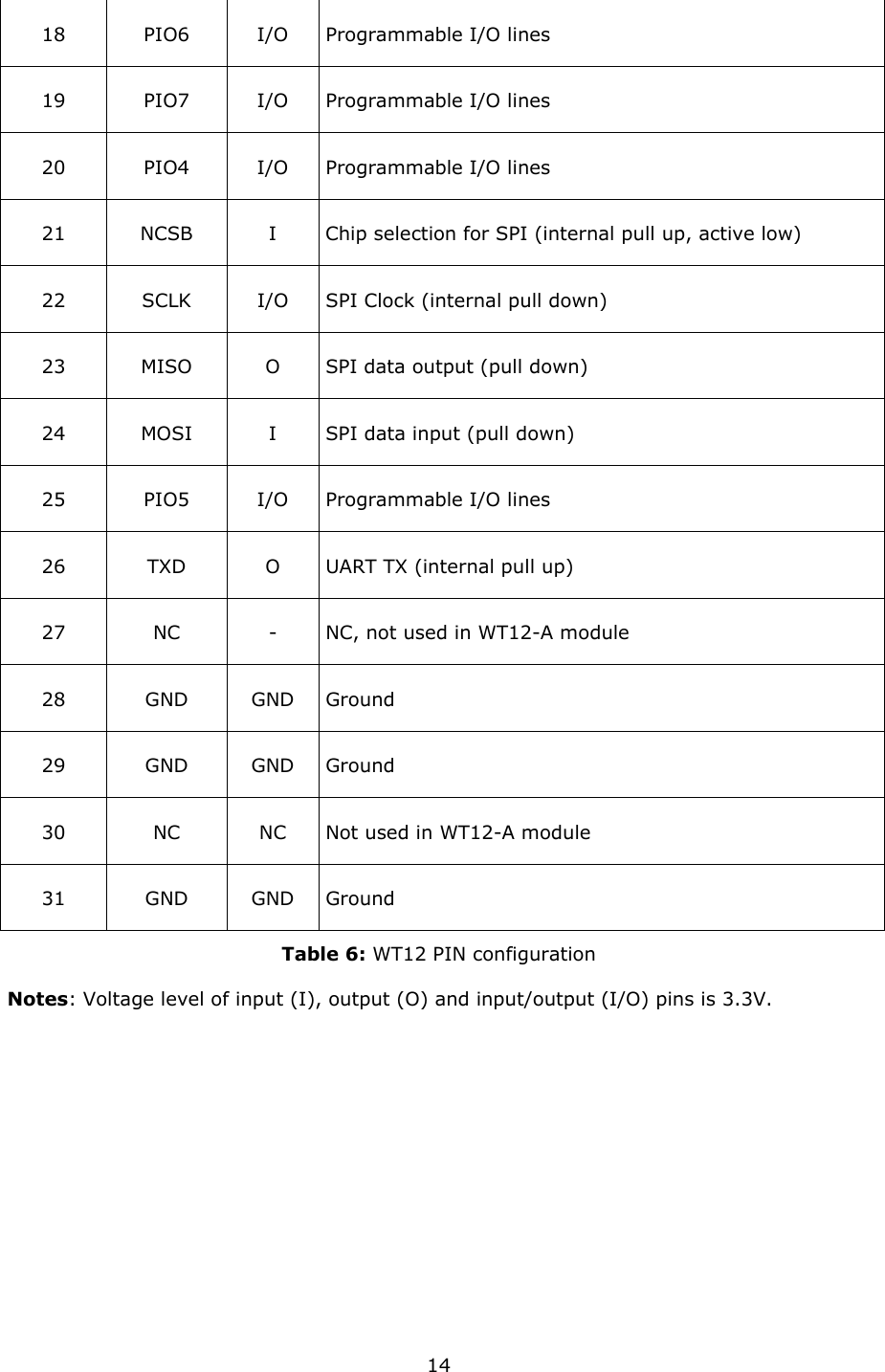
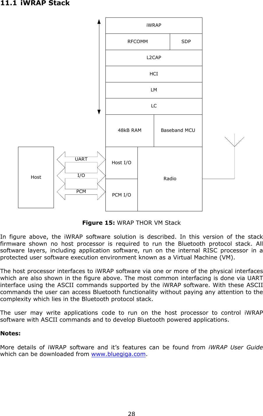
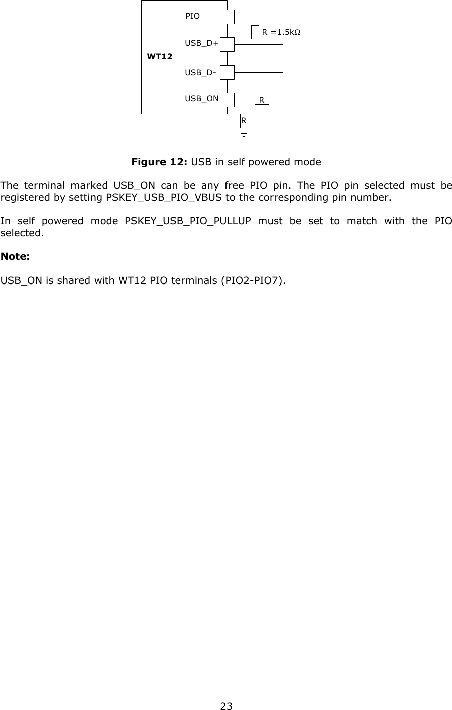
![219.1.1 UART Configuration While RESET is Active The UART interface for WT12 while the chip is being held in reset is tri-state. This will allow the user to daisy chain devices onto the physical UART bus. The constraint on this method is that any devices connected to this bus must tri-state when WT12reset is de-asserted and the firmware begins to run. 9.1.2 UART Bypass Mode Alternatively, for devices that do not tri-state the UART bus, the UART bypass mode on WT12 can be used. The default state of WT12 after reset is de-asserted, this is for the host UART bus to be connected to the WT12 UART, thereby allowing communication to WT12 via the UART. In order to apply the UART bypass mode, a BCCMD command will be issued to WT12 upon this, it will switch the bypass to PIO[7:4] as shown in Figure 6. Once the bypass mode has been invoked, WT12 will enter the deep sleep state indefinitely. In order to re-establish communication with WT12, the chip must be reset so that the default configuration takes affect. It is important for the host to ensure a clean Bluetooth disconnection of any active links before the bypass mode is invoked. Therefore it is not possible to have active Bluetooth links while operating the bypass mode. WT12HostprocessorTestinterfaceRXDCTSRTSTXDAnotherdeviceTXRTSCTSRXUART_TXUART_RTSUART_CTSUART_RXRESETPIO5PIO6PIO7PIO4UART Figure 11: UART bypass mode 9.1.3 Current Consumption in UART Bypass Mode The current consumption for a device in UART Bypass Mode is equal to the values quoted for a device in standby mode.](https://usermanual.wiki/Silicon-Laboratories-Finland/WT12/User-Guide-645424-Page-22.png)
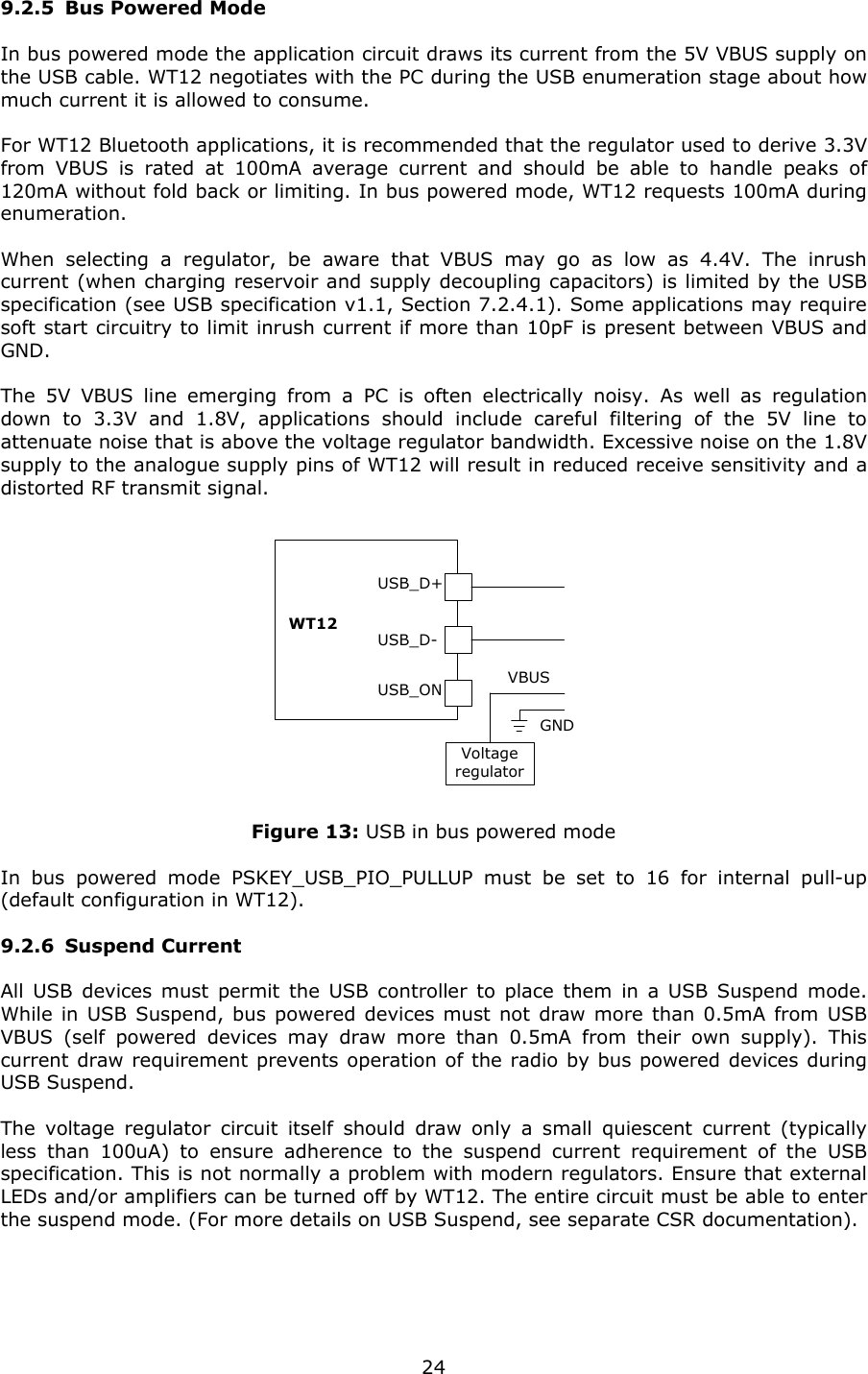
![26USB compliant and can bear the USB logo. Such qualification can be obtained from a USB plug fest or from an independent USB test house. Terminals USB_DP and USB_DN adhere to the USB specification 2.0 (Chapter 7) electrical requirements. 9.2.10 USB 2.0 Compatibility WT12 is compatible with USB v2.0 host controllers; under these circumstances the two ends agree the mutually acceptable rate of 12Mbits/s according to the USB v2.0 specification. 9.3 SPI Interface The synchronous serial port interface (SPI) for interfacing with other digital devices. The SPI port can be used for system debugging. It can also be used for programming the Flash memory. SPI interface is connected using the MOSI, MISO, CSB and CLK pins. 9.4 I/O Parallel Ports The Parallel Input Output (PIO) Port is a general-purpose I/O interface to WT12. The port consists of six programmable, bi-directional I/O lines, PIO[2:7]. Programmable I/O lines can be accessed either via an embedded application running on WT12 or via private channel or manufacturer-specific HCI commands. All PIO lines are configured as inputs with weak pull downs at reset. PIO[2] / USB_PULL_UP (1) This is a multifunction terminal. The function depends on whether WT12 is a USB or UART capable version. On UART versions, this terminal is a programmable I/O. On USB versions, it can drive a pull-up resistor on USB_D+. For application using external RAM this terminal may be programmed for chip select. PIO[3] / USB_WAKE_UP (1) This is a multifunction terminal. On UART versions of WT12 this terminal is a programmable I/O. On USB versions, its function is selected by setting the Persistent Store Key PSKEY_USB_PIO_WAKEUP (0x2cf) either as a programmable I/O or as a USB_WAKE_UP function. PIO[4] / USB_ON (1) This is a multifunction terminal. On UART versions of WT12 this terminal is a programmable I/O. On USB versions, the USB_ON function is also selectable. PIO[5] / USB_DETACH (1) This is a multifunction terminal. On UART versions of WT12 this terminal is a programmable I/O. On USB versions, the USB_DETACH function is also selectable.](https://usermanual.wiki/Silicon-Laboratories-Finland/WT12/User-Guide-645424-Page-27.png)
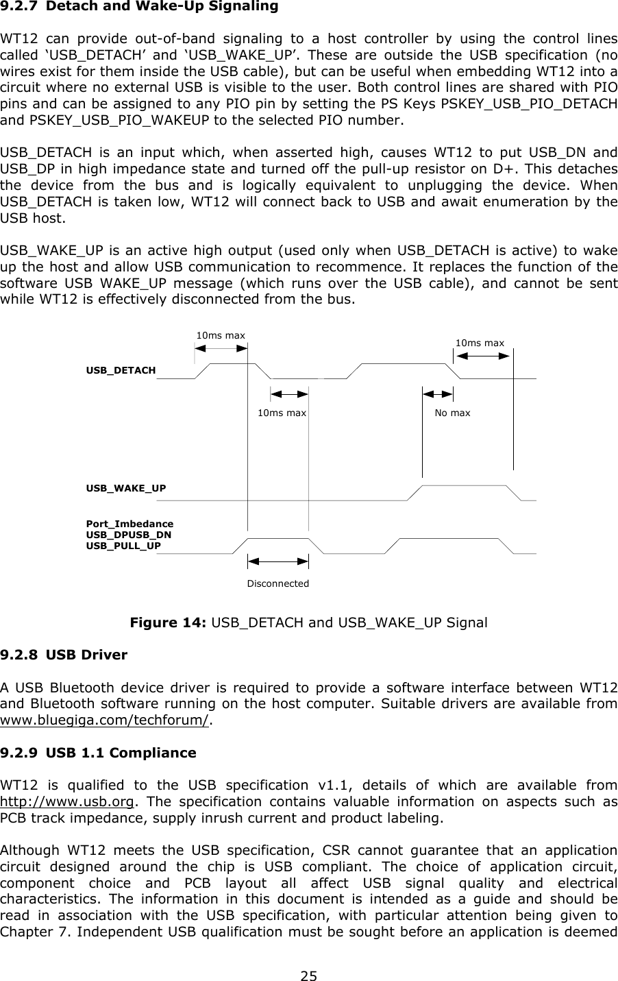
![27PIO[6] / CLK_REQ This is multifunction terminal, its function is determined by Persistent Store Keys. Using PSKEY_CLOCK_REQUEST_ENABLE, (0x246) this terminal can be configured to be low when WT12 is in deep sleep and high when a clock is required. The clock must be supplied within 4ms of the rising edge of PIO[6] to avoid losing timing accuracy in certain Bluetooth operating modes. PIO[7] Programmable I/O terminal. 10. RESET The RESET pin is an active high reset and is internally filtered using the internal low frequency clock oscillator. A reset will be performed between 1.5 and 4.0ms following RESET being active. It is recommended that RESET be applied for a period greater than 5ms. 11. SOFTWARE STACKS WT12 is supplied with Bluetooth v2.0 + EDR compliant stack firmware, which runs on the internal RISC microcontroller. The WT12 software architecture allows Bluetooth processing and the application program to be shared in different ways between the internal RISC microcontroller and an external host processor (if any). The upper layers of the Bluetooth stack (above HCI) can be run either on-chip or on the host processor.](https://usermanual.wiki/Silicon-Laboratories-Finland/WT12/User-Guide-645424-Page-28.png)